5. Electrical and Mechanical
Physical and electrical details of the RP2040 chip.
5.1. Package
Figure 166. Top down view (left, top) and side view (right, top), along with bottom view (left, bottom) of the RP2040 QFN-56 package
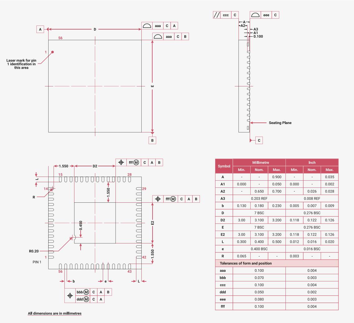
Figure 166 shows the mechanical details of the RP2040 QFN-56 package. The top-left drawing is a top-down view showing dimensions A, D, E, B, and a laser mark for pin 1. The top-right drawing is a side view showing dimensions A, A1, A2, A3, and the seating plane. The bottom-left drawing is a bottom view showing dimensions D2, D, E2, L, b, e, and various pad dimensions. The bottom-right table provides tolerance data for various symbols in millimeters and inches.
| Symbol | Millimetre | Inch | ||||
|---|---|---|---|---|---|---|
| Min. | Nom. | Max. | Min. | Nom. | Max. | |
| A | - | - | 0.900 | - | - | 0.035 |
| A1 | 0.000 | - | 0.050 | 0.000 | - | 0.002 |
| A2 | - | 0.650 | 0.700 | - | 0.026 | 0.028 |
| A3 | 0.203 REF | 0.008 REF | ||||
| b | 0.130 | 0.180 | 0.230 | 0.005 | 0.007 | 0.009 |
| D | 7 BSC | 0.276 BSC | ||||
| D2 | 3.00 | 3.100 | 3.200 | 0.118 | 0.122 | 0.126 |
| E | 7 BSC | 0.276 BSC | ||||
| E2 | 3.00 | 3.100 | 3.200 | 0.118 | 0.122 | 0.126 |
| L | 0.300 | 0.400 | 0.500 | 0.012 | 0.016 | 0.020 |
| e | 0.400 BSC | 0.016 BSC | ||||
| R | 0.065 | - | - | 0.003 | - | - |
| Tolerances of form and position | ||||||
| aaa | 0.100 | 0.004 | ||||
| bbb | 0.070 | 0.003 | ||||
| ccc | 0.100 | 0.004 | ||||
| ddd | 0.050 | 0.002 | ||||
| eee | 0.080 | 0.003 | ||||
| fff | 0.100 | 0.004 | ||||
NOTE
There is no standard size for the central GND pad (or ePad) with QFNs. However, the one on RP2040 is smaller than most. This means that standard 0.4mm QFN-56 footprints provided with CAD tools may need adjusting. This gives the opportunity to route between the central pad and the ones on the periphery, which can help with maintaining power and ground integrity on cheaper PCBs. See Minimal Design Example for an example.
NOTE
Leads have a matte Tin (Sn) finish. Annealing is done post-plating, baking at 150°C for 1 hour. Minimum thickness for lead plating is 8 micromns, and the intermediate layer material is CuFe2P (roughened Copper (Cu)).
5.1.1. Thermal characteristics
The thermal characteristics of the package are shown in Table 611.
Table 611. Thermal data for the RP2040 QFN 56 package.
| \( \theta_{JA} \) (°C/W) | \( \Psi_{JT} \) (°C/W) | \( \Psi_{JB} \) (°C/W) | \( T_J \) (°C) | \( T_T \) (°C) | \( \theta_{JC} \) (°C/W) | \( \theta_{JB} \) (°C/W) |
|---|---|---|---|---|---|---|
| 48.00 | 0.80 | 29.20 | 42.00 | 41.8 | 19.01 | 29.03 |
5.1.2. Recommended PCB Footprint
Figure 167. Recommended PCB Footprint for the RP2040 QFN-56 package
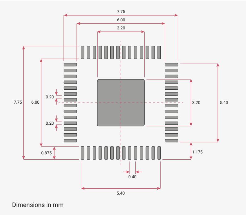
Figure 168. Package marking format
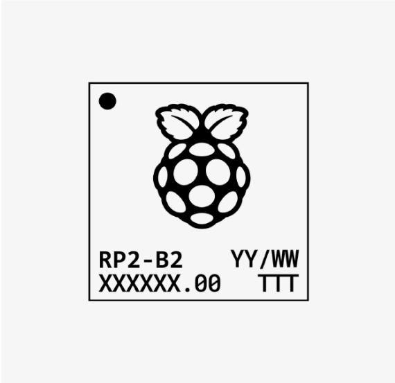
The image shows a square marking area on a light gray background. Inside the square, there is a black dot in the top-left corner. To the right of the dot is the Raspberry Pi logo. Below the logo, the text 'RP2-B2' is printed. To the right of 'RP2-B2' is 'YY/WW'. Below 'RP2-B2' is 'XXXXXX.00'. To the right of 'XXXXXX.00' is 'TTT'.
Table 612. Marking requirements and dimensions
| Line | Step | Item | Coord. X | Coord. Y | Char. Height | Char. Width | Char. Space |
|---|---|---|---|---|---|---|---|
| 1 | 1 | Pin 1 Dot | 0.5 | 6 | 0.5 | 0.5 | |
| 2 | 1 | Logo | 3.5 | 2.395 | 3.83 | 3.05 | |
| 3 | 1 | RP2-B2 | 0.555 | 1.585 | 0.61 | 0.37 | 0.09 |
| 3 | 2 | YY/WW | 4.235 | 1.585 | 0.61 | 0.37 | 0.09 |
| 4 | 1 | XXXXXX.00 | 0.555 | 0.775 | 0.61 | 0.37 | 0.09 |
| 4 | 2 | TTT (optional) | 5.155 | 0.775 | 0.61 | 0.37 | 0.09 |
NOTE
At Line 3, Step 1, the "RP2-B2" marking denotes device name "RP2" and silicon revision "B2."
5.2. Storage conditions
In order to preserve the shelf and floor life of bare RP2040 devices, the recommended storage conditions in line with J-STD (020E & 033D) for RP2040 (classified MSL1) should be kept under 30°C and 85% relative humidity.
5.3. Solder profile
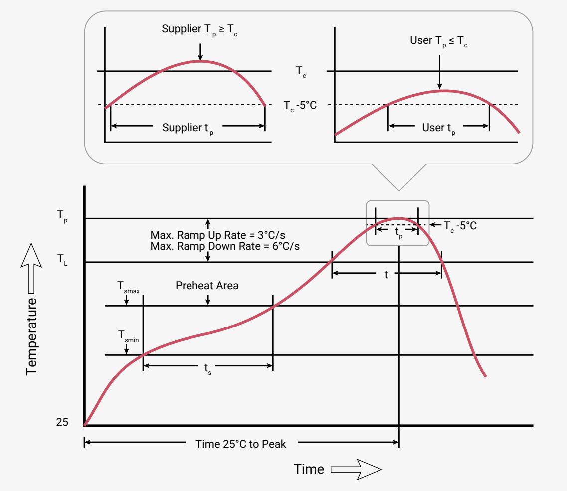
RP2040 is a Pb-free part, with a \( T_p \) value of 260°C.
All temperatures refer to the center of the package, measured on the package body surface that is facing up during assembly reflow (live-bug orientation). If parts are reflowed in other than the normal live-bug assembly reflow orientation (i.e., dead-bug), \( T_p \) shall be within \( \pm 2^\circ\text{C} \) of the live-bug \( T_p \) and still meet the \( T_c \) requirements; otherwise, the profile shall be adjusted to achieve the latter.
Figure 169.
Classification profile
(not to scale)
Supplier \( T_p \geq T_c \)
User \( T_p \leq T_c \)
Max. Ramp Up Rate = 3°C/s
Max. Ramp Down Rate = 6°C/s
Preheat Area
Temperature
Time
Time 25°C to Peak
Time \( t_p \)
Time \( t_s \)
Time \( t \)
Temperature \( T_p \)
Temperature \( T_L \)
Temperature \( T_{smax} \)
Temperature \( T_{smin} \)
Temperature \( T_c \)
Temperature \( T_c - 5^\circ\text{C} \)
NOTE
Reflow profiles in this document are for classification/preconditioning, and are not meant to specify board assembly profiles. Actual board assembly profiles should be developed based on specific process needs and board designs, and should not exceed the parameters in Table 613 .
Table 613. Solder
profile values
| Profile feature | Value |
|---|---|
| Temperature min ( \( T_{smin} \) ) | 150°C |
| Temperature max ( \( T_{smax} \) ) | 200°C |
| Time ( \( t_s \) ) from ( \( T_{smin} \) to \( T_{smax} \) ) | 60 – 120 seconds |
| Ramp-up rate ( \( T_L \) to \( T_p \) ) | 3°C/second max. |
| Liquidous temperature ( \( T_L \) ) | 217°C |
| Time ( \( t_L \) ) maintained above \( T_L \) | 60 to 150 seconds |
| Peak package body temperature ( \( T_p \) ) | 260°C |
| Classification temperature ( \( T_c \) ) | 260°C |
| Time ( \( t_p \) ) within 5°C of the specified classification temperature ( \( T_c \) ) | 30 seconds |
| Ramp-down rate ( \( T_p \) to \( T_L \) ) | 6°C/second max. |
| Time 25°C to peak temperature | 8 minutes max. |
5.4. Compliance
RP2040 is compliant to Moisture Sensitivity Level 1.
RP2040 is compliant to the requirement of REACH Substances of Very High Concern (SVHC) that ECHA announced on 25 June 2020.
RP2040 is compliant to the requirement and standard of Controlled Environment-related Substance of RoHS directive (EU) 2011/65/EU and directive (EU) 2015/863.
Package Level reliability qualifications carried out on RP2040:
- • Temperature Cycling per JESD22-A104
- • HAST per JESD22-A110
- • HTSL per JESD22-A103
NOTE
A tin whiskers test is not performed as RP2040 is a bottom only termination device (QFN package) which not applicable to JEDEC standard (JESD201A).
5.5. Pinout
5.5.1. Pin Locations
Figure 170. RP2040
QFN-56 package
pinout
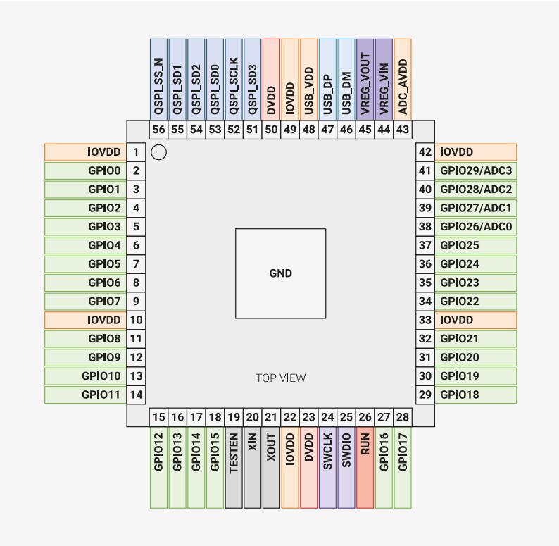
The diagram shows the top view of the RP2040 QFN-56 package. The pins are arranged in a square pattern around a central square labeled 'GND'. The pins are numbered 1 to 56. The functions of the pins are as follows:
| Pin | Function |
|---|---|
| 1 | IOVDD |
| 2 | GPI00 |
| 3 | GPI01 |
| 4 | GPI02 |
| 5 | GPI03 |
| 6 | GPI04 |
| 7 | GPI05 |
| 8 | GPI06 |
| 9 | GPI07 |
| 10 | IOVDD |
| 11 | GPI08 |
| 12 | GPI09 |
| 13 | GPI010 |
| 14 | GPI011 |
| 15 | GPI012 |
| 16 | GPI013 |
| 17 | GPI014 |
| 18 | GPI015 |
| 19 | TESTEN |
| 20 | XIN |
| 21 | XOUT |
| 22 | IOVDD |
| 23 | DVDD |
| 24 | SWCLK |
| 25 | SWDIO |
| 26 | RUN |
| 27 | GPI016 |
| 28 | GPI017 |
| 29 | GPI018 |
| 30 | GPI019 |
| 31 | GPI020 |
| 32 | GPI021 |
| 33 | IOVDD |
| 34 | GPI022 |
| 35 | GPI023 |
| 36 | GPI024 |
| 37 | GPI025 |
| 38 | GPI026/ADC0 |
| 39 | GPI027/ADC1 |
| 40 | GPI028/ADC2 |
| 41 | GPI029/ADC3 |
| 42 | IOVDD |
| 43 | ADC_AVDD |
| 44 | VREG_VIN |
| 45 | VREG_VOUT |
| 46 | USB_DM |
| 47 | USB_DP |
| 48 | USB_VDD |
| 49 | IOVDD |
| 50 | DVDD |
| 51 | QSPL_SD3 |
| 52 | QSPL_SCLK |
| 53 | QSPL_SD0 |
| 54 | QSPL_SD2 |
| 55 | QSPL_SD1 |
| 56 | QSPL_SS_N |
5.5.2. Pin Definitions
5.5.2.1. Pin Types
In the following GPIO Pin table (Table 615), the pin types are defined as shown below.
Table 614. Pin Types
| Pin Type | Direction | Description |
|---|---|---|
| Digital In | Input only | Standard Digital. Programmable Pull-Up, Pull-Down, Slew Rate, Schmitt Trigger and Drive Strength. Default Drive Strength is 4mA. |
| Digital IO | Bi-directional | |
| Digital In (FT) | Input only | Fault Tolerant Digital. These pins are described as Fault Tolerant, which in this case means that very little current flows into the pin whilst it is below 3.63V and IOVDD is 0V. There is also enhanced ESD protection on these pins. Programmable Pull-Up, Pull-Down, Slew Rate, Schmitt Trigger and Drive Strength. Default Drive Strength is 4mA. |
| Digital IO (FT) | Bi-directional | |
| Digital IO / Analogue | Bi-directional (digital), Input (Analogue) | Standard Digital and ADC input. Programmable Pull-Up, Pull-Down, Slew Rate, Schmitt Trigger and Drive Strength. Default Drive Strength is 4mA. |
| USB IO | Bi-directional | These pins are for USB use, and contain internal pull-up and pull-down resistors, as per the USB specification. Note that external 27Ω series resistors are required for USB operation. |
| Analogue (XOSC) | Oscillator input pins for attaching a 12MHz crystal. Alternatively, XIN may be driven by a square wave. |
5.5.2.2. Pin List
Table 615. GPIO pins
| Name | Number | Type | Power Domain | Reset State | Description |
|---|---|---|---|---|---|
| GPIO0 | 2 | Digital IO (FT) | IOVDD | Pull-Down | User IO |
| GPIO1 | 3 | Digital IO (FT) | IOVDD | Pull-Down | User IO |
| GPIO2 | 4 | Digital IO (FT) | IOVDD | Pull-Down | User IO |
| GPIO3 | 5 | Digital IO (FT) | IOVDD | Pull-Down | User IO |
| GPIO4 | 6 | Digital IO (FT) | IOVDD | Pull-Down | User IO |
| GPIO5 | 7 | Digital IO (FT) | IOVDD | Pull-Down | User IO |
| GPIO6 | 8 | Digital IO (FT) | IOVDD | Pull-Down | User IO |
| GPIO7 | 9 | Digital IO (FT) | IOVDD | Pull-Down | User IO |
| GPIO8 | 11 | Digital IO (FT) | IOVDD | Pull-Down | User IO |
| GPIO9 | 12 | Digital IO (FT) | IOVDD | Pull-Down | User IO |
| GPIO10 | 13 | Digital IO (FT) | IOVDD | Pull-Down | User IO |
| GPIO11 | 14 | Digital IO (FT) | IOVDD | Pull-Down | User IO |
| GPIO12 | 15 | Digital IO (FT) | IOVDD | Pull-Down | User IO |
| GPIO13 | 16 | Digital IO (FT) | IOVDD | Pull-Down | User IO |
| GPIO14 | 17 | Digital IO (FT) | IOVDD | Pull-Down | User IO |
| GPIO15 | 18 | Digital IO (FT) | IOVDD | Pull-Down | User IO |
| Name | Number | Type | Power Domain | Reset State | Description |
|---|---|---|---|---|---|
| GPIO16 | 27 | Digital IO (FT) | IOVDD | Pull-Down | User IO |
| GPIO17 | 28 | Digital IO (FT) | IOVDD | Pull-Down | User IO |
| GPIO18 | 29 | Digital IO (FT) | IOVDD | Pull-Down | User IO |
| GPIO19 | 30 | Digital IO (FT) | IOVDD | Pull-Down | User IO |
| GPIO20 | 31 | Digital IO (FT) | IOVDD | Pull-Down | User IO |
| GPIO21 | 32 | Digital IO (FT) | IOVDD | Pull-Down | User IO |
| GPIO22 | 34 | Digital IO (FT) | IOVDD | Pull-Down | User IO |
| GPIO23 | 35 | Digital IO (FT) | IOVDD | Pull-Down | User IO |
| GPIO24 | 36 | Digital IO (FT) | IOVDD | Pull-Down | User IO |
| GPIO25 | 37 | Digital IO (FT) | IOVDD | Pull-Down | User IO |
| GPIO26 / ADC0 | 38 | Digital IO / Analogue | IOVDD / ADC_AVDD | Pull-Down | User IO or ADC input |
| GPIO27 / ADC1 | 39 | Digital IO / Analogue | IOVDD / ADC_AVDD | Pull-Down | User IO or ADC input |
| GPIO28 / ADC2 | 40 | Digital IO / Analogue | IOVDD / ADC_AVDD | Pull-Down | User IO or ADC input |
| GPIO29 / ADC3 | 41 | Digital IO / Analogue | IOVDD / ADC_AVDD | Pull-Down | User IO or ADC input |
Table 616. QSPI pins
| Name | Number | Type | Power Domain | Reset State | Description |
|---|---|---|---|---|---|
| QSPI_SD3 | 51 | Digital IO | IOVDD | QSPI data | |
| QSPI_SCLK | 52 | Digital IO | IOVDD | Pull-Down | QSPI clock |
| QSPI_SD0 | 53 | Digital IO | IOVDD | QSPI data | |
| QSPI_SD2 | 54 | Digital IO | IOVDD | QSPI data | |
| QSPI_SD1 | 55 | Digital IO | IOVDD | QSPI data | |
| QSPI_CSn | 56 | Digital IO | IOVDD | Pull-Up | QSPI chip select |
Table 617. Crystal oscillator pins
| Name | Number | Type | Power Domain | Description |
|---|---|---|---|---|
| XIN | 20 | Analogue (XOSC) | IOVDD | Crystal oscillator. XIN may also be driven by a square wave. |
| XOUT | 21 | Analogue (XOSC) | IOVDD | Crystal oscillator. |
Table 618. Serial wire debug pins
| Name | Number | Type | Power Domain | Reset State | Description |
|---|---|---|---|---|---|
| SWCLK | 24 | Digital In (FT) | IOVDD | Pull-Up | Debug clock |
| SWD | 25 | Digital IO (FT) | IOVDD | Pull-Up | Debug data |
Table 619. Miscellaneous pins
| Name | Number | Type | Power Domain | Reset State | Description |
|---|---|---|---|---|---|
| RUN | 26 | Digital In (FT) | IOVDD | Pull-Up | Chip enable / reset |
| Name | Number | Type | Power Domain | Reset State | Description |
|---|---|---|---|---|---|
| TESTEN | 19 | Digital In | IOVDD | Pull-Down | Test enable (connect to Gnd) |
Table 620. USB pins
| Name | Number | Type | Power Domain | Description |
|---|---|---|---|---|
| USB_DP | 47 | USB IO | USB_VDD | USB Data +ve. 27Ω series resistor required for USB operation |
| USB_DM | 46 | USB IO | USB_VDD | USB Data -ve. 27Ω series resistor required for USB operation |
Table 621. Power supply pins
| Name | Number(s) | Description |
|---|---|---|
| IOVDD | 1, 10, 22, 33, 42, 49 | IO supply |
| DVDD | 23, 50 | Core supply |
| VREG_VIN | 44 | Voltage regulator input supply |
| VREG_VOUT | 45 | Voltage regulator output |
| USB_VDD | 48 | USB supply |
| ADC_AVDD | 43 | ADC supply |
| GND | 57 | Common ground connection via central pad |
5.5.3. Pin Specifications
The following electrical specifications are obtained from characterisation over the specified temperature and voltage ranges, as well as process variation, unless the specification is marked as 'Simulated'. In this case, the data is for information purposes only, and is not guaranteed.
5.5.3.1. Absolute Maximum Ratings
Table 622. Absolute maximum ratings for digital IO (Standard and Fault Tolerant)
| Parameter | Symbol | Minimum | Maximum | Units | Comment |
|---|---|---|---|---|---|
| I/O Supply Voltage | IOVDD | -0.5 | 3.63 | V | |
| Voltage at IO | V PIN | -0.5 | IOVDD + 0.5 | V |
5.5.3.2. ESD Performance
Table 623. ESD performance for all pins, unless otherwise stated
| Parameter | Symbol | Maximum | Units | Comment |
|---|---|---|---|---|
| Human Body Model | HBM | 2 | kV | Compliant with JEDEC specification JS-001-2012 (April 2012) |
| Parameter | Symbol | Maximum | Units | Comment |
|---|---|---|---|---|
| Human Body Model Digital (FT) pins only | HBM | 4 | kV | Compliant with JEDEC specification JS-001-2012 (April 2012) |
| Charged Device Model | CDM | 500 | V | Compliant with JESD22-C101E (December 2009) |
5.5.3.3. Thermal Performance
Table 624. Thermal Performance
| Parameter | Symbol | Minimum | Typical | Maximum | Units | Comment |
|---|---|---|---|---|---|---|
| Case Temperature | \( T_C \) | -40 | 85 | °C |
5.5.3.4. IO Electrical Characteristics
Table 625. Digital IO characteristics - Standard and FT unless otherwise stated
| Parameter | Symbol | Minimum | Maximum | Units | Comment |
|---|---|---|---|---|---|
| Pin Input Leakage Current | \( I_{IN} \) | 1 | μA | ||
| Input Voltage High @ IOVDD=1.8V | \( V_{IH} \) | \( 0.65 * IOVDD \) | \( IOVDD + 0.3 \) | V | |
| Input Voltage High @ IOVDD=2.5V | \( V_{IH} \) | 1.7 | \( IOVDD + 0.3 \) | V | |
| Input Voltage High @ IOVDD=3.3V | \( V_{IH} \) | 2 | \( IOVDD + 0.3 \) | V | |
| Input Voltage Low @ IOVDD=1.8V | \( V_{IL} \) | -0.3 | \( 0.35 * IOVDD \) | V | |
| Input Voltage Low @ IOVDD=2.5V | \( V_{IL} \) | -0.3 | 0.7 | V | |
| Input Voltage Low @ IOVDD=3.3V | \( V_{IL} \) | -0.3 | 0.8 | V | |
| Input Hysteresis Voltage @ IOVDD=1.8V | \( V_{HYS} \) | \( 0.1 * IOVDD \) | V | Schmitt Trigger enabled | |
| Input Hysteresis Voltage @ IOVDD=2.5V | \( V_{HYS} \) | 0.2 | V | Schmitt Trigger enabled | |
| Input Hysteresis Voltage @ IOVDD=3.3V | \( V_{HYS} \) | 0.2 | V | Schmitt Trigger enabled | |
| Output Voltage High @ IOVDD=1.8V | \( V_{OH} \) | 1.24 | IOVDD | V | \( I_{OH} = 2, 4, 8 \) or 12mA depending on setting |
| Parameter | Symbol | Minimum | Maximum | Units | Comment |
|---|---|---|---|---|---|
| Output Voltage High @ IOVDD=2.5V | \( V_{OH} \) | 1.78 | IOVDD | V | \( I_{OH} = 2, 4, 8 \) or 12mA depending on setting |
| Output Voltage High @ IOVDD=3.3V | \( V_{OH} \) | 2.62 | IOVDD | V | \( I_{OH} = 2, 4, 8 \) or 12mA depending on setting |
| Output Voltage Low @ IOVDD=1.8V | \( V_{OL} \) | 0 | 0.3 | V | \( I_{OL} = 2, 4, 8 \) or 12mA depending on setting |
| Output Voltage Low @ IOVDD=2.5V | \( V_{OL} \) | 0 | 0.4 | V | \( I_{OL} = 2, 4, 8 \) or 12mA depending on setting |
| Output Voltage Low @ IOVDD=3.3V | \( V_{OL} \) | 0 | 0.5 | V | \( I_{OL} = 2, 4, 8 \) or 12mA depending on setting |
| Pull-Up Resistance | \( R_{PU} \) | 50 | 80 | k \( \Omega \) | |
| Pull-Down Resistance | \( R_{PD} \) | 50 | 80 | k \( \Omega \) | |
| Maximum Total IOVDD current | \( I_{IOVDD\_MAX} \) | 50 | mA | Sum of all current being sourced by GPIO and QSPI pins | |
| Maximum Total VSS current due to IO (IOVSS) | \( I_{IOVSS\_MAX} \) | 50 | mA | Sum of all current being sunk into GPIO and QSPI pins |
Table 626. USB IO characteristics
| Parameter | Symbol | Minimum | Maximum | Units | Comment |
|---|---|---|---|---|---|
| Pin Input Leakage Current | \( I_{IN} \) | 1 | \( \mu \) A | ||
| Single Ended Input Voltage High | \( V_{IHSE} \) | 2 | V | ||
| Single Ended Input Voltage Low | \( V_{ILSE} \) | 0.8 | V | ||
| Differential Input Voltage High | \( V_{IHDIFF} \) | 0.2 | V | ||
| Differential Input Voltage Low | \( V_{ILDIFF} \) | -0.2 | V | ||
| Output Voltage High | \( V_{OH} \) | 2.8 | USB_VDD | V | |
| Output Voltage Low | \( V_{OL} \) | 0 | 0.3 | V | |
| Pull-Up Resistance - RPU2 | \( R_{PU2} \) | 0.873 | 1.548 | k \( \Omega \) |
| Parameter | Symbol | Minimum | Maximum | Units | Comment |
|---|---|---|---|---|---|
| Pull-Up Resistance - RPU1&2 | R PU1&2 | 1.398 | 3.063 | kΩ | |
| Pull-Down Resistance | R PD | 14.25 | 15.75 | kΩ |
Table 627. ADC characteristics
| Parameter | Symbol | Minimum | Maximum | Units | Comment |
|---|---|---|---|---|---|
| ADC Input Voltage Range | V PIN_ADC | 0 | ADC_AVDD | V | |
| Effective Number of Bits | ENOB | 8.7 | bits | See Section 4.9.3 | |
| Resolved Bits | 12 | bits | |||
| ADC Input Impedance | R IN_ADC | 100 | kΩ |
Table 628. Oscillator pin characteristics when using a Square Wave input
| Parameter | Symbol | Minimum | Maximum | Units | Comment |
|---|---|---|---|---|---|
| Input Voltage High | V IH | 0.65*IOVDD | IOVDD + 0.3 | V | XIN only. XOUT floating |
| Input Voltage Low | V IL | 0 | 0.35*IOVDD | V | XIN only. XOUT floating |
See Section 2.16 for more details on the Oscillator, and Minimal Design Example for information on crystal usage.
5.5.3.5. Interpreting GPIO output voltage specifications
The GPIOs on RP2040 have four different output drive strengths, which are nominally called 2, 4, 8 and 12mA modes. These are not hard limits, nor do they mean that they will always be sourcing (or sinking) the selected amount of milliamps. The amount of current a GPIO sources or sinks is dependent on the load attached to it. It will attempt to drive the output to the IOVDD level (or 0V in the case of a logic 0), but the amount of current it is able to source is limited, which will be dependent on the selected drive strength. Therefore the higher the current load is, the lower the voltage will be at the pin. At some point, the GPIO will be sourcing so much current, that the voltage is so low, it won't be recognised as a logic 1 by the input of a connected device. The purpose of the output specifications in Table 625 are to try and quantify how much lower the voltage can be expected to be, when drawing specified amounts of current from the pin.
The Output High Voltage (V OH ) is defined as the lowest voltage the output pin can be when driven to a logic 1 with a particular selected drive strength; e.g., 4mA being sourced by the pin whilst in 4mA drive strength mode. The Output Low Voltage is similar, but with a logic 0 being driven.
In addition to this, the sum of all the IO currents being sourced (i.e. when outputs are being driven high) from the IOVDD bank (essentially the GPIO and QSPI pins), must not exceed I IOVDD_MAX . Similarly, the sum of all the IO currents being sunk (i.e. when the outputs are being driven low) must not exceed I IOVSS_MAX .
Figure 171. Typical Current vs Voltage curves of a GPIO output.
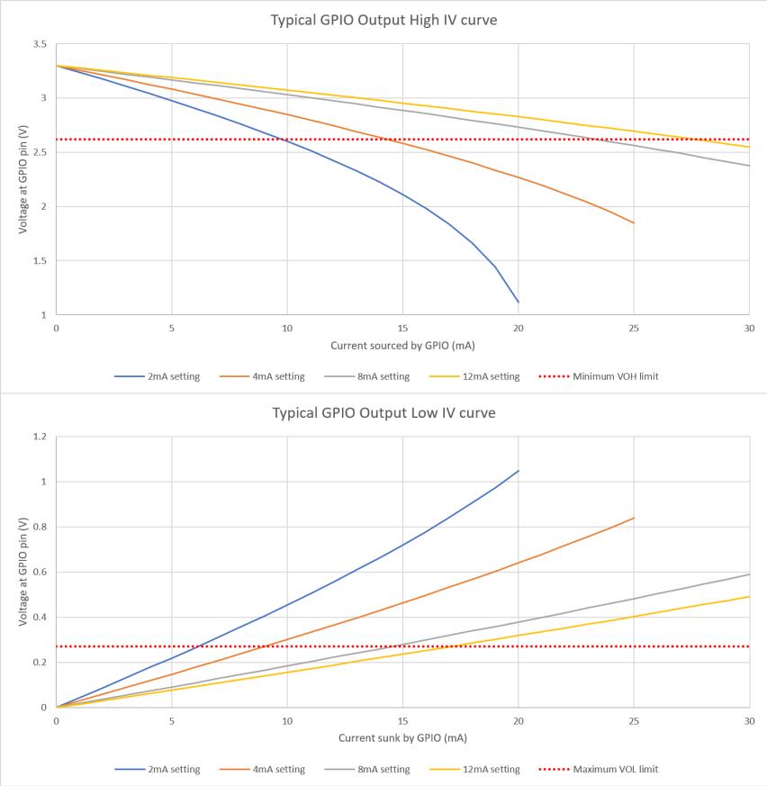
The figure consists of two graphs. The top graph, titled 'Typical GPIO Output High IV curve', plots Voltage at GPIO pin (V) on the y-axis (1 to 3.5) against Current sourced by GPIO (mA) on the x-axis (0 to 30). It shows four curves for different drive settings: 2mA (blue), 4mA (orange), 8mA (grey), and 12mA (yellow). A red dotted line indicates the Minimum VOH limit at approximately 2.6V. The bottom graph, titled 'Typical GPIO Output Low IV curve', plots Voltage at GPIO pin (V) on the y-axis (0 to 1.2) against Current sunk by GPIO (mA) on the x-axis (0 to 30). It shows four curves for the same drive settings. A red dotted line indicates the Maximum VOL limit at approximately 0.28V.
Figure 171 shows the effect on the output voltage as the current load on the pin increases. You can clearly see the effect of the different drive strengths; the higher the drive strength, the closer the output voltage is to IOVDD (or 0V) for a given current. The minimum \( V_{OH} \) and maximum \( V_{OL} \) limits are shown in red. You can see that at the specified current for each drive strength, the voltage is well within the allowed limits, meaning that this particular device could drive a lot more current and still be within \( V_{OH}/V_{OL} \) specification. This is a typical part at room temperature, there will be a spread of other devices which will have voltages much closer to this limit. Of course, if your application doesn't need such tightly controlled voltages, then you can source or sink more current from the GPIO than the selected drive strength setting, but experimentation will be required to determine if it indeed safe to do so in your application, as it will be outside the scope of this specification.
5.5.3.6. Pin IO Delays
These delays include PIO's input/output mapping logic, IO muxing, and the actual pad delays into a nominal load of 5 pF. Min/max is over the extremes of process variation, voltage (1.1 V +/- 10%) and temperature (-40 C to 125 C).
These delays assume an IOVDD of 1.8 V, with
PADS_VSEL
set. At IOVDD = 3.3 V, the delay is significantly lower, and the range is smaller.
The flops themselves have a typical setup time of 10.6 ps and hold time of 2.2 ps. The IO delays between flops and pads must be taken into account.
For minimum and maximum output delays, from
CLK_SYS
arriving at any flop in PIO to the data being valid at a particular GPIO pad see Table 629.
Table 629. Pin minimum and maximum delays from flop to pad, in nanoseconds.
| Pad output | Min delay (ns) | Max delay (ns) |
|---|---|---|
| GPIO0 | 2.27 | 7.10 |
| GPIO1 | 2.31 | 7.07 |
| Pad output | Min delay (ns) | Max delay (ns) |
|---|---|---|
| GPIO2 | 2.33 | 7.08 |
| GPIO3 | 2.24 | 7.00 |
| GPIO4 | 2.30 | 7.07 |
| GPIO5 | 2.34 | 7.10 |
| GPIO6 | 2.32 | 7.10 |
| GPIO7 | 2.39 | 7.09 |
| GPIO8 | 2.34 | 7.09 |
| GPIO9 | 2.38 | 7.08 |
| GPIO10 | 2.33 | 7.07 |
| GPIO11 | 2.36 | 7.08 |
| GPIO12 | 2.35 | 7.04 |
| GPIO13 | 2.31 | 7.08 |
| GPIO14 | 2.38 | 7.06 |
| GPIO15 | 2.33 | 7.05 |
| GPIO16 | 2.34 | 7.09 |
| GPIO17 | 2.37 | 7.09 |
| GPIO18 | 2.37 | 7.04 |
| GPIO19 | 2.27 | 7.10 |
| GPIO20 | 2.38 | 7.09 |
| GPIO21 | 2.05 | 7.10 |
| GPIO22 | 2.34 | 7.07 |
| GPIO23 | 2.16 | 7.05 |
| GPIO24 | 2.12 | 7.06 |
| GPIO25 | 2.26 | 7.10 |
| GPIO26 | 2.32 | 7.09 |
| GPIO27 | 2.26 | 7.08 |
| GPIO28 | 2.34 | 7.09 |
| GPIO29 | 2.30 | 7.07 |
For minimum and maximum input delays, from pad input to the input synchroniser, see Table 630 .
Table 630. Pin minimum and maximum delays from pad input to input synchroniser, in nanoseconds.
| Pad output | Min delay (ns) | Max delay (ns) |
|---|---|---|
| GPIO1 | 1.89 | 5.22 |
| GPIO2 | 1.84 | 5.25 |
| GPIO3 | 1.83 | 5.24 |
| GPIO4 | 1.90 | 5.17 |
| GPIO5 | 1.90 | 5.14 |
| Pad output | Min delay (ns) | Max delay (ns) |
|---|---|---|
| GPIO6 | 1.91 | 5.19 |
| GPIO7 | 1.91 | 5.14 |
| GPIO8 | 1.95 | 5.14 |
| GPIO9 | 1.96 | 5.12 |
| GPIO10 | 1.95 | 5.11 |
| GPIO11 | 1.92 | 5.16 |
| GPIO12 | 1.92 | 5.15 |
| GPIO13 | 1.94 | 5.16 |
| GPIO14 | 1.90 | 5.18 |
| GPIO15 | 1.92 | 5.15 |
| GPIO16 | 1.95 | 5.13 |
| GPIO17 | 1.95 | 5.12 |
| GPIO18 | 1.95 | 5.10 |
| GPIO19 | 1.95 | 5.12 |
| GPIO21 | 2.07 | 4.98 |
| GPIO23 | 1.98 | 5.06 |
| GPIO24 | 1.97 | 5.07 |
| GPIO25 | 1.97 | 5.08 |
| GPIO26 | 1.96 | 5.12 |
| GPIO27 | 1.94 | 5.13 |
| GPIO28 | 1.95 | 5.13 |
| GPIO29 | 1.99 | 5.10 |
For minimum and maximum input delays over all corners, from pad input to state machine IN data flops (synchronisers bypassed) see Table 631 .
Table 631. Pin minimum and maximum delays from pad input to state machine IN data flops (synchronisers bypassed), in nanoseconds.
| Pad input | Min delay (ns) | Max delay (ns) |
|---|---|---|
| GPIO1 | 2.22 | 5.45 |
| GPIO2 | 2.25 | 5.49 |
| GPIO3 | 2.23 | 5.18 |
| GPIO4 | 2.24 | 5.41 |
| GPIO5 | 2.30 | 5.65 |
| GPIO6 | 2.25 | 5.48 |
| GPIO7 | 2.26 | 5.50 |
| GPIO8 | 2.30 | 5.51 |
| GPIO9 | 2.25 | 5.68 |
| GPIO10 | 2.34 | 5.71 |
| GPIO11 | 2.28 | 5.47 |
| Pad input | Min delay (ns) | Max delay (ns) |
|---|---|---|
| GPIO12 | 2.29 | 5.40 |
| GPIO13 | 2.25 | 5.47 |
| GPIO14 | 2.24 | 5.41 |
| GPIO15 | 2.23 | 5.47 |
| GPIO16 | 2.30 | 5.42 |
| GPIO17 | 2.28 | 5.44 |
| GPIO18 | 2.28 | 5.34 |
| GPIO19 | 2.30 | 5.50 |
| GPIO21 | 2.16 | 5.79 |
| GPIO23 | 2.33 | 5.53 |
| GPIO24 | 2.28 | 5.60 |
| GPIO25 | 2.29 | 5.53 |
| GPIO26 | 2.28 | 5.38 |
| GPIO27 | 2.27 | 5.39 |
| GPIO28 | 2.24 | 5.28 |
| GPIO29 | 2.33 | 5.47 |
5.5.3.6.1. Effects of IOVDD
All of the IO delays given above assume IOVDD = 1.8V. Increasing IOVDD to 3.3V reduces the pad delays quite significantly, and the pad delay is a large fraction of the delays reported above. See Table 632 for a summary of best and worst pad delays at 1.8V and 3.3V.
Table 632. Best and worst pad delays at 1.8V and 3.3V.
| Path type | IOVDD | Min delay (ns) | Max delay (ns) |
|---|---|---|---|
| Output | 1.8V | 1.54 | 3.65 |
| Output | 3.3V | 1.11 | 2.14 |
| Input | 1.8V | 0.63 | 1.06 |
| Input | 3.3V | 0.47 | 0.76 |
Changing IOVDD does not affect any logic in the core domain, so these differences can be added to the IO delay tables above to estimate the IO delay ranges at IOVDD = 3.3V (see Table 633 ).
Table 633. IO delay ranges at IOVDD = 3.3V.
| Path group | IOVDD | Min delay (ns) | Max delay (ns) |
|---|---|---|---|
| Output | 1.8V | 2.12 | 7.10 |
| Output | 3.3V | 1.69 | 5.59 |
| Input to sync | 1.8V | 1.83 | 5.25 |
| Input to sync | 3.3V | 1.67 | 4.95 |
| Input to SM | 1.8V | 2.16 | 5.79 |
| Input to SM | 3.3V | 2.00 | 5.49 |
5.6. Power Supplies
Table 634. Power Supply Specifications
| Power Supply | Supplies | Min | Typ | Max | Units |
|---|---|---|---|---|---|
| IOVDD a | Digital IO | 1.62 | 1.8 / 3.3 | 3.63 | V |
| DVDD b | Digital core | 1.05 | 1.1 | 1.16 | V |
| VREG_VIN | Voltage regulator | 1.62 | 1.8 / 3.3 | 3.63 | V |
| USB_VDD | USB PHY | 3.135 | 3.3 | 3.63 | V |
| ADC_AVDD c | ADC | 1.62 | 3.3 | 3.63 | V |
a If IOVDD <2.5V, GPIO VOLTAGE_SELECT registers should be adjusted accordingly. See Section 2.9 for details.
b
Short term transients should be within +/-100mV. If using 200MHz for
clk_sys
as described in
Section 2.15.3
, set DVDD to 1.15V.
c ADC performance will be compromised at voltages below 2.97V
5.7. Power Consumption
5.7.1. Peripheral power consumption
Baseline readings are taken with only clock sources and essential peripherals (
BUSCTRL
,
BUSFAB
,
VREG
, Resets, ROM, SRAMs) active in the
WAKE_EN0
/
WAKE_EN1
registers. Clocks are set to default clock settings. Each peripheral is activated in turn by enabling all clock sources for the peripheral in the
WAKE_EN0
/
WAKE_EN1
registers. Current consumption is the increase in current when the peripheral clocks are enabled.
Table 635. Baseline power consumption
| Peripheral | Typical DVDD Current Consumption (µA/MHz) |
|---|---|
| DMA | 2.6 |
| I2C0 | 3.9 |
| I2C1 | 3.8 |
| IO + Pads | 23.6 |
| PIO0 | 12.3 |
| PIO1 | 12.5 |
| PWM | 5.0 |
| RTC | 1.1 |
| SIO | 1.9 |
| SPIO | 1.7 |
| SPI1 | 1.8 |
| Timer | 1.2 |
| UART0 | 3.5 |
| UART1 | 3.7 |
| Watchdog | 1.0 |
| XIP | 37.6 |
Because of fixed external reference clocks of 48 MHz, as well as the variable system clock input, ADC and USBCTRL power consumption does not vary linearly with system clock (as it does for other peripherals which only have system and/or peripheral clock inputs). Absolute DVDD current consumption of the ADC and USBCTRL blocks at standard clocks (system clock of 125 MHz) is given below:
Table 636. Baseline power consumption for ADC and USBCTRL
| Peripheral | Typical DVDD Current Consumption (µA/MHz) |
|---|---|
| ADC | 0.1 |
| USBCTRL | 1.3 |
5.7.2. Power consumption for typical user cases
The following data shows the current consumption of various power supplies on 3 each of typical (tt), fast (ff) and slow (ss) corner RP2040 devices, with four different software use-cases.
Image: Note icon
NOTEFor power consumption of the Raspberry Pi Pico, please see the Raspberry Pi Pico Datasheet .
Firstly, 'Popcorn' (Media player demo) using the VGA, SD Card, and Audio board. This demo uses VGA video, I2S audio and 4-bit SD Card access, with a system clock frequency of 48MHz.
Image: Note icon
NOTEFor more details of the VGA board see the Hardware design with RP2040 book.
Secondly, the BOOTSEL mode of RP2040. These measurements are made both with and without USB activity on the bus, using a Raspberry Pi 4 as a host.
The third use-case uses the
hello_dormant
binary which puts RP2040 into a low power state,
DORMANT
mode.
The final use-case uses the
hello_sleep
binary code which puts RP2040 into a low power state,
SLEEP
mode.
Table 637 has two columns per power supply, 'Typical Average Current' and 'Maximum Average Current'. The former is the current averaged over several seconds that you might expect a typical RP2040 to consume at room temperature and nominal voltage (e.g., DVDD=1.1V, IOVDD=3.3V, etc). The 'Maximum Average Current' is the maximum current consumption (again averaged over several seconds) you might expect to see on a worst-case RP2040 device, across the temperature extremes, and maximum voltage (e.g., DVDD=1.21V, etc).
Image: Note icon
NOTEThe 'Popcorn' consumption measurements depend on the video being displayed at the time. The 'Typical' values are obtained over several seconds of video, with varied colour and intensity. The 'Maximum' values are measured during periods of white video, when the required current is at its highest.
Table 637. Power Consumption
| Software Use-case | Typical Average DVDD Current | Max. Average DVDD current | Typical Average IOVDD Current | Max. Average IOVDD current | Typical Average USB_VDD Current | Max. Average USB_VDD current | Units |
|---|---|---|---|---|---|---|---|
| Popcorn | 10.9 | 16.6 | 24.8 | 35.5 | - | - | mA |
| BOOTSEL mode - Active | 9.4 | 14.7 | 1.2 | 4.3 | 1.4 | 2.0 | mA |
| BOOTSEL mode - Idle | 9.0 | 14.3 | 1.2 | 4.3 | 0.2 | 0.6 | mA |
| Dormant | 0.18 | 4.2 | - | - | - | - | mA |
| Software Use-case | Typical Average DVDD Current | Max. Average DVDD current | Typical Average IOVDD Current | Max. Average IOVDD current | Typical Average USB_VDD Current | Max. Average USB_VDD current | Units |
|---|---|---|---|---|---|---|---|
| Sleep | 0.39 | 4.5 | - | - | - | - | mA |
5.7.2.1. Power Consumption versus frequency
To give an indication of the relationship between the core frequency that RP2040 is operating at, and the current consumed by the DVDD supply, Figure 172 shows the measured results of a typical RP2040 device, continuously running FFT calculations on both cores, at various core clock frequencies. Figure 172 also shows the effects of case temperature, and DVDD voltage upon the current consumption.
Figure 172. DVDD Current vs Core Frequency of a typical RP2040 device, whilst running FFT calculations
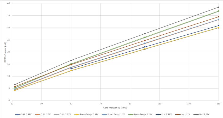
The graph plots DVDD Current (mA) on the y-axis (0 to 40) against Core Frequency (MHz) on the x-axis (10 to 150). There are nine data series representing combinations of three temperatures (Cold, Room Temp, Hot) and three DVDD voltages (0.99V, 1.1V, 1.21V). The lines show a positive linear correlation between frequency and current. Higher temperatures and higher DVDD voltages result in higher current consumption across all frequencies.
| Core Frequency (MHz) | Cold: 0.99V | Cold: 1.1V | Cold: 1.21V | Room Temp: 0.99V | Room Temp: 1.1V | Room Temp: 1.21V | Hot: 0.99V | Hot: 1.1V | Hot: 1.21V |
|---|---|---|---|---|---|---|---|---|---|
| 10 | 4.5 | 5.5 | 6.5 | 4.5 | 5.5 | 6.5 | 4.5 | 5.5 | 6.5 |
| 50 | 12.5 | 14.5 | 16.5 | 12.5 | 14.5 | 16.5 | 12.5 | 14.5 | 16.5 |
| 90 | 20.5 | 22.5 | 24.5 | 20.5 | 22.5 | 24.5 | 20.5 | 22.5 | 24.5 |
| 130 | 28.5 | 30.5 | 32.5 | 28.5 | 30.5 | 32.5 | 28.5 | 30.5 | 32.5 |
| 150 | 32.5 | 34.5 | 36.5 | 32.5 | 34.5 | 36.5 | 32.5 | 34.5 | 36.5 |
Appendix A: Register Field Types
Standard types
RW:
- • Read/Write
- • Read operation returns the register value
- • Write operation updates the register value
RO:
- • Read-only
- • Read operation returns the register value
- • Write operations are ignored
WO:
- • Write-only
- • Read operation returns 0
- • Write operation updates the register value
Clear types
SC
- • Self-Clearing
- • Writing a 1 to a bit in an SC field will trigger an event, once the event is triggered the bit clears automatically
- • Writing a 0 to a bit in an SC field does nothing
WC
- • Write-Clear
- • Writing a 1 to a bit in a WC field will write that bit to 0
- • Writing a 0 to a bit in a WC field does nothing
- • Read operation returns the register value
FIFO types
These fields are used for reading and writing data to and from FIFOs. Accompanying registers provide FIFO control and status. There is no fixed format for the control and status registers, as they are specific to each FIFO interface.
RWF
- • Read/Write FIFO
- • Reading this field returns data from a FIFO
- ◦ When the read is complete, the data value is removed from the FIFO
- ◦ If the FIFO is empty, a default value will be returned; the default value is specific to each FIFO interface
- • Data written to this field is pushed to a FIFO, Behaviour when the FIFO is full is specific to each FIFO interface
- • Read and write operations may access different FIFOs
RF
- • Read FIFO
- • Functions the same as RWF, but read-only
WF
- • Write FIFO
- • Functions the same as RWF, but write-only
Appendix B: Errata
Hardware blocks are listed alphabetically. Errata are listed numerically under the relevant block.
Bootrom
RP2040-E9
| Reference | RP2040-E9 |
| Summary | ROM bootloader cannot boot directly into XIP cache-as-SRAM |
| Description | The XIP cache can be used as an additional 16kB SRAM bank when XIP caching is disabled ( Section 2.6.3.1 ). The UF2 bootloader supports RAM-only UF2 binaries, which it loads directly into memory, and enters via a watchdog reboot. A single UF2 binary can initialise both the XIP cache contents and main system memory, and the cache is disabled by the bootloader, so that cache contents be written. However, the watchdog reset re-enables the cache, so booting directly into the cache-as-SRAM alias causes an immediate bus fault. The cache contents are preserved, but can not be accessed immediately post-boot. |
| Workaround | Add code in main SRAM to re-disable XIP caching before accessing the cache-as-SRAM alias. When entering a RAM-only UF2 binary, the bootloader selects the lowest loaded address in either main SRAM or cache-as-SRAM as the entry point, preferring main SRAM if both are loaded. Additionally, if the
|
| Affects | RP2040B0, RP2040B1, RP2040B2 |
| Fixed by | Documentation |
RP2040-E14
| Reference | RP2040-E14 |
| Summary | Sparse or mis-aligned flash-binary UF2 may not be written to flash correctly by the UF2 bootloader |
| Description | A RP2040 UF2 file consists of 256-byte pages of data, each marked to be written at a certain address by the UF2 bootloader. A flash-binary UF2 is one of these for which every 256-byte page is marked to be written at a 256-byte-aligned address in flash. When writing flash, an entire 4kB flash sector must be erased at a time before any pages within that sector can be (re-)written. The UF2 bootloader does not require the flash-binary UF2 to include data for all pages within a sector. In that case the whole sector will first be erased, any present pages will be written, and the rest of the 4kB sector will be left undefined. This mechanism works as expected when the partially-filled sector is at the end of the binary, which is of course commonplace, as a binary does not need to be a multiple of 4kB long. If however, the partially-filled sector occurs at the start of the binary (i.e. the binary is not aligned on a 4kB page) or if a partially-filled sector appears in the middle of the binary (i.e. the binary is sparse/non-contiguous), then the UF2 file may be written incorrectly. Note that the vast majority of UF2s generated by the SDK are indeed aligned on a 4kB boundary and contiguous, however it is possible for the SDK to produce a misaligned or non-contiguous binary by modifying the linker scripts, or putting extreme alignment requirements on static data. It is also possible that other languages or tools might produce binaries that are not 4kB-aligned or contiguous. |
| Workaround | The workaround is to include data for all the pages in any 4kB sector (other than the last) that contains data for some pages. This is handled for you automatically by the
|
| Affects | RP2040B0, RP2040B1, RP2040B2 |
| Fixed by | Documentation / Software |
Clocks
RP2040-E7
| Reference | RP2040-E7 |
| Summary | ROSC and XOSC
COUNT
registers are unreliable |
| Description | The ROSC and XOSC
COUNT
registers are intended to be used in the configuration of components like PHYs and PLLs where microsecond scale delays are required and NOP loops are inadequate because the
clk_sys
frequency is variable. However due to a synchronisation issue the ROSC:
COUNT
and XOSC:
COUNT
registers are unreliable. |
| Workaround | Do not use ROSC:
COUNT
or XOSC:
COUNT |
| Affects | RP2040B0, RP2040B1, RP2040B2 |
| Fixed by | Not fixed, do not use. These registers are not used by the C SDK. |
RP2040-E10
| Reference | RP2040-E10 |
| Summary | BADWRITE field in ROSC STATUS register is unreliable |
| Description | The BADWRITE field in the ROSC STATUS register was intended to report when invalid values had been written to other ROSC registers. However due to internal bugs the ROSC: STATUS . BADWRITE field is unreliable. |
| Workaround | Do not use ROSC: STATUS . BADWRITE field |
| Affects | RP2040B0, RP2040B1, RP2040B2 |
| Fixed by | Not fixed, do not use. This field is not used by the C SDK. |
DMA
RP2040-E12
| Reference | RP2040-E12 |
| Summary | Reading DMA WRITE_ADDR and READ_ADDR registers when an address-wrapping or non-incrementing transfer sequence is in progress gives wrong values |
| Description | The DMA's internal WRITE_ADDR and READ_ADDR registers are incremented every time the DMA issues a new address to its bus pipeline. If the processor reads these registers whilst a sequence of transfers is in progress, the value reported by the DMA is adjusted downward by the number of in-flight transfers (i.e. issued to the bus pipeline and not yet completed) times the individual transfer size in bytes. This logic was added to ensure that reading READ_ADDR and WRITE_ADDR reflects addresses where the read/write has completed , not merely where the address has been issued. This logic does not take into account that READ_ADDR and WRITE_ADDR do not increment linearly for some transfer modes, specifically, when CTRL.INCR_WRITE == 0, CTRL.INCR_READ == 0 or CTRL.RING_SIZE != 0. |
| Workaround | Instead of checking READ_ADDR or WRITE_ADDR to monitor the progress of a transfer sequence, check TRANS_COUNT . TRANS_COUNT has similar in-flight adjustment logic, but is not affected by this erratum because it always decrements linearly. The correct values of READ_ADDR and WRITE_ADDR can be calculated based on their initial values and TRANS_COUNT . |
| Affects | RP2040B0, RP2040B1, RP2040B2 |
| Fixed by | Documentation |
RP2040-E13
| Reference | RP2040-E13 |
| Summary | After aborting a channel, the ABORT status clears prematurely, and an interrupt may be asserted |
| Description | The DMA ABORT register is used to cancel an ongoing sequence of transfers, for example when a channel is stuck on an inactive peripheral DREQ. If, at the point the abort is triggered, the channel currently has any transfers in flight (i.e. the read cycle of the transfer has taken place, but the write cycle has not), the ABORT bit does not wait for these in-flight transfers to complete before clearing. When the in-flight transfers complete, because the ABORT bit was prematurely cleared, the DMA treats this as a normal completion. This sets the channel's interrupt status flag, assuming CTRL.IRQ_QUIET has not been set. |
| Workaround | Before aborting a channel, clear its interrupt enable. After aborting a channel, poll the CTRL.BUSY bit to wait for completion (not the ABORT bit), clear the spurious IRQ, and restore the interrupt enable. |
| Affects | RP2040B0, RP2040B1, RP2040B2 |
| Fixed by | Software |
GPIO / ADC
RP2040-E6
| Reference | RP2040-E6 |
| Summary | GPIO digital inputs not disabled for ADC pins by default |
| Description | GPIO26-29 are shared with ADC inputs AIN0-3. The GPIO digital input is enabled after RUN is released. If the pins are connected to an analogue signal to measure, there could be unexpected signal levels on these pads. This is unlikely to cause a problem as the digital inputs have hysteresis enabled by default. |
| Workaround | If analogue inputs are used, the digital input should be disabled as early as possible after startup. This is done in the RP2040B2 bootrom and early on in SDK platform setup code on RP2040B0 and RP2040B1. If user wishes to use digital inputs, they must be enabled. |
| Affects | RP2040B0, RP2040B1 |
| Fixed by | RP2040B2 bootrom. Fixed on RP2040B0 and RP2040B1 in SDK. Custom user code should disable these inputs early on. |
RP2040-E11
| Reference | RP2040-E11 |
| Summary | DNL error peaks in ADC |
| Description | The RP2040 ADC has a DNL that is mostly flat, and below 1 LSB. However at four values – 512, 1,536, 2,560, and 3,584 – the ADC's DNL error peaks above this value. The ENOB for the ADC has been reduced from 9-bits (simulated) to 8.7-bits (measured), see Section 4.9.3 . The DNL errors will somewhat limit the performance of the ADC dependent on use case. |
| Workaround | None |
| Affects | RP2040B0, RP2040B1, RP2040B2 |
| Fixed by | Not fixed. |
USB
RP2040-E2
| Reference | RP2040-E2 |
| Summary | USB device endpoint abort is not cleared. |
| Description | The USB device controller ( Section 4.1 ) has the ability to abort any pending transactions on an endpoint by setting that endpoint's bit in the EP_ABORT register. Due to a logic error, the USB device controller will reply with NAKs forever on all endpoints if a transaction is initiated for any endpoint with the EP_ABORT bit set. |
| Workaround | Do not use the EP_ABORT bits. |
| Affects | RP2040B0, RP2040B1 |
| Fixed by | RP2040B2 |
RP2040-E3
| Reference | RP2040-E3 |
| Summary | USB host: interrupt endpoint buffer done flag can be set with incorrect buffer select. |
| Description | The USB host has two types of transactions: normal software initiated transfer, and interrupt transfers, where the host polls an interrupt endpoint after a specific amount of time. For example, polling a mouse every 1ms to check for movement. Interrupt transfer are single buffered, but the controller doesn't reset the buffer selector to zero. This means that if a software initiated transfer happened then the interrupt transfer can potentially raise the buffer done flag with BUF1 selected instead of BUF0 . The fix is to ignore the BUFF_CPU_SHOULD_HANDLE register for interrupt endpoints. |
| Workaround | |
| Affects | RP2040B0, RP2040B1, RP2040B2 |
| Fixed by | Software |
RP2040-E4
| Reference | RP2040-E4 |
| Summary | USB host writes to upper half of buffer status in single buffered mode. |
| Description | The USB host maintains a buffer selector which switches between BUF0 and BUF1 . This should only be toggled in double buffered mode but is toggled in single buffered mode too. For a transaction lasting multiple packets (i.e. length more than 8 bytes in low speed mode, and length more than 64 bytes in full speed mode), the buffer status can be written back to the BUF1 half of the status register when the buffer select is incorrectly set to BUF1 . Note this does not affect reading new buffer information from the buffer control register, as the controller ignores the buffer selector in single buffered mode when reading the buffer control register. |
| Workaround | Shift endpoint control register to the right by 16 bits if the buffer selector is BUF1 . You can use BUFF_CPU_SHOULD_HANDLE find the value of the buffer selector when the buffer was marked as done. |
| Affects | RP2040B0, RP2040B1, RP2040B2 |
| Fixed by | Software |
RP2040-E5
| Reference | RP2040-E5 |
| Summary | USB device fails to exit RESET state on busy USB bus. |
| Description | The USB bus RESET state is triggered by the host sending SE0 for 10ms to the device. The USB device controller requires 800µs of idle ( J-state ) after a bus reset before moving to the CONNECTED state. Without this idle time, the USB device does not connect and will not receive any packets from the host, and so does not enumerate. A device reset happens just after the device is plugged in. Although a host will wait before talking to a newly-reset device, other devices attached to the same USB hub may also be communicating with the host. USB 2.0 and USB 3.0 hubs have one or more transaction translators, which facilitate low speed and full speed transactions on a higher speed bus. It depends on the hub design, but a transaction translator is usually shared between a few ports. As the RP2040 USB device is full speed, its traffic when connected to a hub will come via a transaction translator. This means that if you have another device plugged in next to an RP2040, the RP2040 is likely to see some messages from the host addressed to the other device. If the device is not very active, for example, a mouse that is polled every 8ms, this is not a problem. However some devices, such as a USB serial port, are polled every 30-50µs. In this case the bus is very active, and will cause the RP2040 to never exit RESET state and not connect. There is a hardware fix in RP2040B2 which avoids the need for 800µs of IDLE time after RESET state. There is a software workaround for this issue (see workaround section). A user can also work around this by closing the USB serial port or any other offending devices while connecting their RP2040 and then re-opening their USB serial port. On a larger hub, the problem may be fixed by moving the RP2040 far away (onto a different transaction translator) from the offending device. For example, connecting the RP2040 to port 1 of a 7 port hub, and connecting the USB serial console to port 7, may solve the issue. Connecting the RP2040 to a separate USB hub to any busy devices will also fix the problem. |
| Workaround | Use software to force USB device controller to see idle USB bus for 800µs to move the device from the RESET state to the CONNECTED state. This fix uses internal debug logic that is connected to GPIO15 for a short amount of time (~800µs). This forces the controller to see DP as a logical 1 (and DM as logical 0) to make the USB Device controller believe there is a J-state on the USB bus. GPIO15 does not need to be tied in any particular way for this fix to work. Instead, we can force the input path in software using the Section 2.19 input override feature. See https://github.com/raspberrypi/pico-sdk/blob/master/src/rp2_common/pico_fix/rp2040_usb_device_enumeration/rp2040_usb_device_enumeration.c . NOTE The workaround takes control of GPIO 15 during a device reset, so you need to be sure that you are not using GPIO 15 for anything else during a device reset before using the workaround. A device reset happens after the first connection, but may also happen at other times under the host's control. Using the workaround with TinyUSB and the SDK is easy, as the above source file is included by the library
It is safe (and inexpensive) to enable the software workaround even when using versions of RP2040 which include the fix in hardware. |
| Affects | RP2040B0, RP2040B1 |
| Fixed by | RP2040B2. Software workaround on RP2040B0, RP2040B1. The workaround isn't present in the USB mass storage code in the bootrom. The software workaround requires use of GPIO15 during USB bus reset. |
RP2040-E15
| Reference | RP2040-E15 |
| Summary | USB Device controller will hang if certain bus errors occur during an IN transfer. |
| Description | The USB Device controller enters an unrecoverable state if the following critical sequence of events occurs:
This sequence is known to occur with the downstream-facing ports on a Raspberry Pi 4 or a Raspberry Pi 400 and Bulk IN endpoints with data buffer sizes of more than 50 bytes. In this case, the integrated USB2.0 hub incorrectly determines the remaining full-speed frame time in anticipation of a SOF packet from the host, and erroneously transmits an IN token which results in the later ACK reply being corrupted and replaced by the propagated SOF packet. This type of data corruption is not properly handled by the device state machine, and the device controller must be reset. This sequence has not been seen to occur on commodity USB2.0 hubs, nor on Root Ports that are not provided by a VL805 xHCI controller. |
| Workarounds | 1) VL805 firmware version 0138c1 An updated firmware has been pushed to the
DEFAULT
channel in the
raspberrypi-bootloader
Apt package on Pi 4 products. This corrects the erroneous hub time calculation. This firmware update is not automatically applied, users must run
2) Linux Kernel xHCI driver patch A kernel update is available for the Raspberry Pi 4-series products that, for VL805 firmware versions earlier than 0138c1, avoids enqueueing single Transfer Descriptors to the controller for affected endpoints during the last microframe of a full-speed frame. This update is available in the raspberrypi-kernel Apt package. 2) SDK v1.5.0 / TinyUSB 0.15.0 TinyUSB starting at version 0.15.0 adds a workaround for this erratum, and this version is picked up in the v1.5.0 release of the SDK. The
The TinyUSB workaround is not necessary for implementations that will never be connected to a vulnerable VL805 port, for example in a circuit design where RP2040 is directly connected to an on-board hub. The workaround can be disabled by defining
|
| Affects | RP2040B0, RP2040B1, RP2040B2 |
| Fixed by | Documentation, Software |
RP2040-E16
| Reference | RP2040-E16 |
| Summary | Inadequate synchronisation of USB status signals |
| Description | Within the USB peripheral, certain Host and Device controller events cross from
The following signals lack appropriate synchronisation methods:
The bootrom's USB bootloader chains
|
| Workaround | Run
clk_sys
faster than
clk_usb
by at least 10% when the peripheral is in use. Signalling of quasi-static bus states such as reset, suspend, and resume are not affected by this erratum, so
clk_sys
can be lower in these cases. |
| Affects | RP2040B0, RP2040B1, RP2040B2 |
| Fixed by | Documentation, software. Not fixed in the RP2040 bootrom. |
Watchdog
RP2040-E1
| Reference | RP2040-E1 |
| Summary | Watchdog count is decremented twice per tick. |
| Description | The watchdog ( Section 4.7 ) has a 24-bit counter, that decrements every tick, starting from a user defined value set in LOAD register. There is a logic error which means the counter is decremented twice per tick, instead of once per tick. In a recommended setup where the tick occurs at 1µs intervals, this halves the maximum time between resetting the watchdog counter from ~16.7 seconds to ~8.3 seconds. |
| Workaround | Use double the desired value in LOAD . |
| Affects | RP2040B0, RP2040B1, RP2040B2 |
| Fixed by | Documentation, Software |
XIP Flash
RP2040-E8
| Reference | RP2040-E8 |
| Summary | Race condition when aborting an XIP DMA stream and immediately starting a new stream |
| Description | The XIP DMA streaming hardware allows a linear sequences of flash reads to proceed in the background, and be read by the DMA, without subjecting the DMA to the bus stalls caused by a normal XIP-window access. A stream is begun by writing to the STREAM_ADDR register, followed by STREAM_CTR , and can be aborted midway by writing 0 to STREAM_CTR . When a stream is aborted in this way, there is sufficient time for software to load a new address and begin a new stream whilst the final SPI/QSPI access of the aborted stream is still in progress. This causes the newly-loaded stream address to be incremented once before the first data transfer of the new stream sequence, so the entire stream takes place at a 4-byte offset. |
| Workaround | After clearing
STREAM_CTR
, immediately perform one dummy read from the uncached XIP window, e.g.
(void)*(io_ro_32*)XIP_NOCACHE_NOALLOC_BASE;
. If an XIP stream transfer is still in progress, this dummy read will stall until that transfer completes. It is then safe to begin a new stream by writing to
STREAM_ADDR
followed by
STREAM_CTR
. |
| Affects | RP2040B0, RP2040B1, RP2040B2 |
| Fixed by | Documentation, Software |
Appendix C: Availability
Raspberry Pi understands the value to customers of long term availability of product and therefore aims to continue supply for as long as practically possible. We expect RP2040 to remain in production until at least January 2041.
Support
For support see the Pico section of the Raspberry Pi website , and post questions on the Raspberry Pi forum .
Ordering code
RP2040 can be ordered in bulk from Raspberry Pi Direct .
Table 638. Part Number
| Model | Order Code | Minimal Order Quantity | RRP | Equivalent price per chip |
|---|---|---|---|---|
| 7" reel of 500 × RP2040 chips | SC0914(7) | 1+ pcs / Bulk | US$400.00 | US$0.80 |
| 13" reel of 3,400 × RP2040 chips | SC0914(13) | 1+ pcs / Bulk | US$2,380.00 | US$0.70 |
NOTE
RRP was correct at time of publication and excludes taxes.
Documentation Release History
20 February 2025
- • Updated register field types descriptions to use the improved RP2350 wording.
- • Add information about running Dual Cortex M0+ processor cores at 200MHz.
15 October 2024
- • Corrected minor typos and formatting issues.
- • Switched back to separate release histories per PDF.
02 May 2024
- • Corrected minor typos and formatting issues.
02 February 2024
- • Corrected minor typos and formatting issues.
- • Updated ROSC register information.
- • Updated to include the new recommended part number for crystals used with RP2040.
14 June 2023
- • Corrected minor typos and formatting issues.
03 March 2023
- • Corrected minor typos and formatting issues.
- • Added errata E15 .
- • Added package marking specifications.
- • Added RP2040 baseline power consumption figures.
01 December 2022
- • Corrected minor typos and formatting issues.
- • Added RP2040 availability information.
- • Added RP2040 storage conditions and thermal characteristics.
- • Replaced SDK library documentation with links to the online version.
30 June 2022
- • Corrected minor typos and formatting issues.
17 June 2022
- • Corrected minor typos and formatting issues.
- • RP2040 now qualified to -40°C, minimum operating temperature changed from -20°C to -40°C.
- • Increased PLL min VCO from 400MHz to 750MHz for improved stability across operating conditions.
- • Added errata E12 , E13 and E14 .
04 November 2021
- • Corrected minor typos and formatting issues.
- • Improved documentation on USB double buffering.
- • Updated links to documentation.
03 November 2021
- • Corrected minor typos and formatting issues.
- • Fixed some register access types and descriptions.
- • Added core 1 launch sequence info.
- • Described SDK "panic" handling.
- • Updated picotool documentation.
30 September 2021
- • Corrected minor typos and formatting issues.
- • Added information about B2 release.
- • Updated errata for B2 release.
23 June 2021
- • Corrected minor typos and formatting issues.
- • Updated information on ADC.
- • Added errata E11 .
07 June 2021
- • Corrected minor typos and formatting issues.
- • Added SDK release history.
13 April 2021
- • Corrected minor typos and formatting issues.
- • Clarified that all source code in the documentation is under the 3-Clause BSD license.
07 April 2021
- • Corrected minor typos and formatting issues.
- • Added errata E10 .
05 March 2021
- • Corrected minor typos and formatting issues.
- • Improved pinout diagram.
23 February 2021
- • Corrected minor typos and formatting issues.
- • Changed font.
- • Added additional documentation on sink/source limits for RP2040.
- • Made major improvements to SWD documentation.
- • Added errata E7 , E8 and E9 .
01 February 2021
- • Corrected minor typos and formatting issues.
- • Made small improvements to PIO documentation.
- • Added missing TIMER2 and TIMER3 registers to DMA.
26 January 2021
- • Corrected minor typos and formatting issues.
- • Added extra information about using DMA with ADC.
- • Clarified M0+ and SIO CPUID registers.
- • Added more discussion of Timers.
- • Renamed books and optimised size of output PDFs.
21 January 2021
- • Initial release.

The Raspberry Pi logo, which is a stylized white raspberry fruit with a small green leaf on top, set against a dark red background.
Raspberry Pi
Raspberry Pi is a trademark of Raspberry Pi Ltd