1. Introduction
RP2350 is a new family of microcontrollers from Raspberry Pi that offers major enhancements over RP2040. Key features include:
- • Dual Cortex-M33 or Hazard3 processors at 150 MHz
- • 520 kB on-chip SRAM, in 10 independent banks
- • 8 kB of one-time-programmable storage (OTP)
- • Up to 16 MB of external QSPI flash or PSRAM through dedicated QSPI bus
- • Additional 16 MB flash or PSRAM through optional second chip-select
- • On-chip switched-mode power supply to generate core voltage
- • Optional low-quiescent-current LDO mode for sleep states
- • 2 × on-chip PLLs for internal or external clock generation
- • GPIOs are 5 V-tolerant (powered) and 3.3 V-failsafe (unpowered)
- • Security features:
- ◦ Optional boot signing, enforced by on-chip mask ROM, with key fingerprint in OTP
- ◦ Protected OTP storage for optional boot decryption key
- ◦ Global bus filtering based on Arm or RISC-V security/privilege levels
- ◦ Peripherals, GPIOs, and DMA channels individually assignable to security domains
- ◦ Hardware mitigations for fault injection attacks
- ◦ Hardware SHA-256 accelerator
- • Peripherals:
- ◦ 2 × UARTs
- ◦ 2 × SPI controllers
- ◦ 2 × I2C controllers
- ◦ 24 × PWM channels
- ◦ USB 1.1 controller and PHY, with host and device support
- ◦ 12 × PIO state machines
- ◦ 1 × HSTX peripheral
Table 1 shows the RP2350 family of devices, including options for QFN-80 (10 × 10 mm) and QFN-60 (7 × 7 mm) packages, with and without flash-in-package.
Table 1. RP2350 device family
| Product | Package | Internal Flash | GPIO | Analogue Inputs |
|---|---|---|---|---|
| RP2350A | QFN-60 | None | 30 | 4 |
| RP2350B | QFN-80 | None | 48 | 8 |
| RP2354A | QFN-60 | 2 MB | 30 | 4 |
| RP2354B | QFN-80 | 2 MB | 48 | 8 |
1.1. The chip
Dual Cortex-M33 or Hazard3 processors access RP2350's memory and peripherals via AHB and APB bus fabric.
Figure 1. A system overview of the RP2350 chip
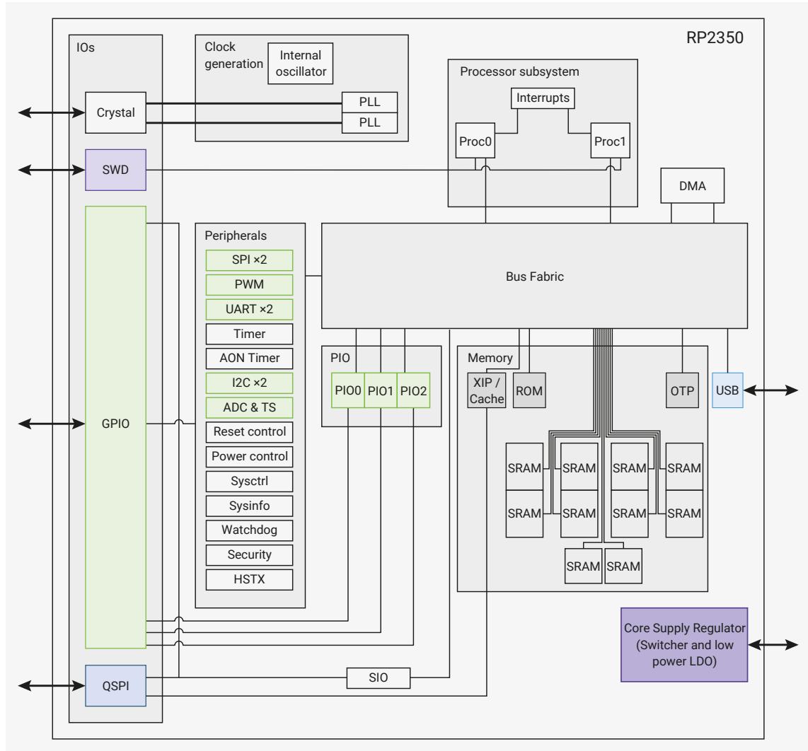
Code may execute directly from external memory through a dedicated QSPI memory interface in the execute-in-place subsystem (XIP). The cache improves XIP performance significantly. Both flash and RAM can attach via this interface.
Debug is available via the SWD interface. This allows an external host to load, run, halt and inspect software running on the system, or configure the execution trace output.
Internal SRAM can contain code or data. It is addressed as a single 520 kB region, but physically partitioned into 10 banks to allow simultaneous parallel access from different managers. All SRAM supports single-cycle access.
A high-bandwidth system DMA offloads repetitive data transfer tasks from the processors.
GPIO pins can be driven directly via single-cycle IO (SIO), or from a variety of dedicated logic functions such as the hardware SPI, I2C, UART and PWM. Programmable IO controllers (PIO) can provide a wider variety of IO functions, or supplement the number of fixed-function peripherals.
A USB controller with embedded PHY provides FS/LS Host or Device connectivity under software control.
Four or eight ADC inputs (depending on package size) are shared with GPIO pins.
Two PLLs provide a fixed 48 MHz clock for USB or ADC, and a flexible system clock up to 150 MHz. A crystal oscillator provides a precise reference for the PLLs.
An internal voltage regulator supplies the core voltage, so you need generally only supply the IO voltage. It operates as a
switched mode buck converter when the system is awake, providing up to 200 mA at a variable output voltage, and can switch to a low-quiescent-current LDO mode when the system is asleep, providing up to 1 mA for state retention.
The system features low-power states where unused logic is powered off, supporting wakeup from timer or IO events. The amount of SRAM retained during power-down is configurable.
The internal 8 kB one-time-programmable storage (OTP) contains chip information such as unique identifiers, can be used to configure hardware and bootrom security features, and can be programmed with user-supplied code and data.
The built-in bootrom implements direct boot from flash or OTP, and serial boot from USB or UART. Code signature enforcement is supported for all boot media, using a key fingerprint registered in internal OTP storage. OTP can also store decryption keys for encrypted boot, preventing flash contents from being read externally.
RISC-V architecture support is implemented by dynamically swapping the Cortex-M33 (Armv8-M) processors with Hazard3 (RV32IMAC+) processors. Both architectures are available on all RP2350-family devices. The RISC-V cores support debug over SWD, and can be programmed with the same SDK as the Arm cores.
1.2. Pinout reference
This section provides a quick reference for pinout and pin functions. Full details, including electrical specifications and package drawings, can be found in Chapter 14 .
1.2.1. Pin locations
1.2.1.1. QFN-60 (RP2350A)
Figure 2. RP2350
Pinout for QFN-60
7×7mm (reduced ePad
size)
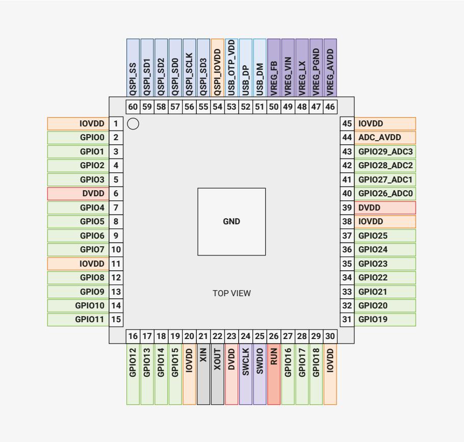
The diagram shows the top view of the QFN-60 package with pins numbered 1 to 60. The pins are arranged in a square grid with a central GND pad. The pin functions are as follows:
| Pin | Function |
|---|---|
| 1 | IOVDD |
| 2 | GPI00 |
| 3 | GPI01 |
| 4 | GPI02 |
| 5 | GPI03 |
| 6 | DVDD |
| 7 | GPI04 |
| 8 | GPI05 |
| 9 | GPI06 |
| 10 | GPI07 |
| 11 | IOVDD |
| 12 | GPI08 |
| 13 | GPI09 |
| 14 | GPI010 |
| 15 | GPI011 |
| 16 | GPI012 |
| 17 | GPI013 |
| 18 | GPI014 |
| 19 | GPI015 |
| 20 | IOVDD |
| 21 | XIN |
| 22 | XOUT |
| 23 | DVDD |
| 24 | SWCLK |
| 25 | SWDIO |
| 26 | RUN |
| 27 | GPI016 |
| 28 | GPI017 |
| 29 | GPI018 |
| 30 | IOVDD |
| 31 | GPI019 |
| 32 | GPI020 |
| 33 | GPI021 |
| 34 | GPI022 |
| 35 | GPI023 |
| 36 | GPI024 |
| 37 | GPI025 |
| 38 | IOVDD |
| 39 | DVDD |
| 40 | GPI026_ADC0 |
| 41 | GPI027_ADC1 |
| 42 | GPI028_ADC2 |
| 43 | GPI029_ADC3 |
| 44 | ADC_AVDD |
| 45 | IOVDD |
| 46 | VREG_AVDD |
| 47 | VREG_PGND |
| 48 | VREG_LX |
| 49 | VREG_VIN |
| 50 | VREG_FB |
| 51 | USB_DM |
| 52 | USB_DP |
| 53 | USB_OTP_VDD |
| 54 | QSPL_IOVDD |
| 55 | QSPL_SD3 |
| 56 | QSPL_SCLK |
| 57 | QSPL_SD0 |
| 58 | QSPL_SD2 |
| 59 | QSPL_SD1 |
| 60 | QSPL_SS |
1.2.1.2. QFN-80 (RP2350B)
Figure 3. RP2350
Pinout for QFN-80
10×10mm (reduced
ePad size)
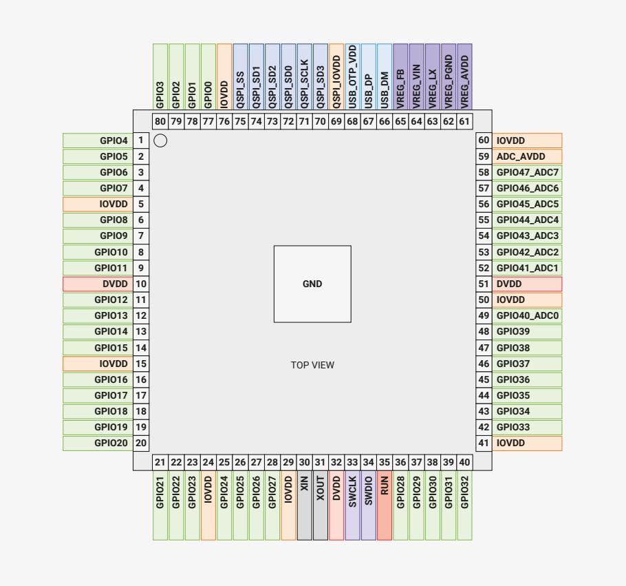
The diagram shows the pinout for the RP2350B QFN-80 package. The pins are arranged in a square grid with a central GND pad. The top view shows the following pin functions:
- Pin 1: GPIO4
- Pin 2: GPIO5
- Pin 3: GPIO6
- Pin 4: GPIO7
- Pin 5: IOVDD
- Pin 6: GPIO8
- Pin 7: GPIO9
- Pin 8: GPIO10
- Pin 9: GPIO11
- Pin 10: DVDD
- Pin 11: GPIO12
- Pin 12: GPIO13
- Pin 13: GPIO14
- Pin 14: GPIO15
- Pin 15: IOVDD
- Pin 16: GPIO16
- Pin 17: GPIO17
- Pin 18: GPIO18
- Pin 19: GPIO19
- Pin 20: GPIO20
- Pin 21: GPIO21
- Pin 22: GPIO22
- Pin 23: GPIO23
- Pin 24: IOVDD
- Pin 25: GPIO24
- Pin 26: GPIO25
- Pin 27: GPIO26
- Pin 28: GPIO27
- Pin 29: IOVDD
- Pin 30: XIN
- Pin 31: XOUT
- Pin 32: DVDD
- Pin 33: SWCLK
- Pin 34: SWDIO
- Pin 35: RUN
- Pin 36: GPIO28
- Pin 37: GPIO29
- Pin 38: GPIO30
- Pin 39: GPIO31
- Pin 40: GPIO32
- Pin 41: IOVDD
- Pin 42: GPIO33
- Pin 43: GPIO34
- Pin 44: GPIO35
- Pin 45: GPIO36
- Pin 46: GPIO37
- Pin 47: GPIO38
- Pin 48: GPIO39
- Pin 49: GPIO40_ADC0
- Pin 50: IOVDD
- Pin 51: DVDD
- Pin 52: GPIO41_ADC1
- Pin 53: GPIO42_ADC2
- Pin 54: GPIO43_ADC3
- Pin 55: GPIO44_ADC4
- Pin 56: GPIO45_ADC5
- Pin 57: GPIO46_ADC6
- Pin 58: GPIO47_ADC7
- Pin 59: ADC_AVDD
- Pin 60: IOVDD
- Pin 61: VREG_AVDD
- Pin 62: VREG_LX
- Pin 63: VREG_VIN
- Pin 64: VREG_FB
- Pin 65: USB_DM
- Pin 66: USB_DP
- Pin 67: USB_OTP_VDD
- Pin 68: QSPI_LOVDD
- Pin 69: QSPI_SD3
- Pin 70: QSPI_SCLK
- Pin 71: QSPI_SD0
- Pin 72: QSPI_SD2
- Pin 73: QSPI_SD1
- Pin 74: QSPI_SS
- Pin 75: IOVDD
- Pin 76: GPIO0
- Pin 77: GPIO1
- Pin 78: GPIO2
- Pin 79: GPIO3
- Pin 80: GPIO3
1.2.2. Pin descriptions
Table 2. The function
of each pin is briefly
described here. Full
electrical
specifications can be
found in
Chapter 14
.
| Name | Description |
|---|---|
| GPIOx | General-purpose digital input and output. RP2350 can connect one of a number of internal peripherals to each GPIO, or control GPIOs directly from software. |
| GPIOx/ADCy | General-purpose digital input and output, with analogue-to-digital converter function. The RP2350 ADC has an analogue multiplexer which can select any one of these pins, and sample the voltage. |
| QSPiX | Interface to a SPI, Dual-SPI or Quad-SPI flash or PSRAM device, with execute-in-place support. These pins can also be used as software-controlled GPIOs, if they are not required for flash access. |
| USB_DM and USB_DP | USB controller, supporting Full Speed device and Full/Low Speed host. A 27Ω series termination resistor is required on each pin, but bus pullups and pulldowns are provided internally. These pins can be used as software-controlled GPIOs, if USB is not required. |
| XIN and XOUT | Connect a crystal to RP2350's crystal oscillator. XIN can also be used as a single-ended CMOS clock input, with XOUT disconnected. The USB bootloader defaults to a 12MHz crystal or 12MHz clock input, but this can be configured via OTP. |
| RUN | Global asynchronous reset pin. Reset when driven low, run when driven high. If no external reset is required, this pin can be tied directly to IOVDD. |
| SWCLK and SWDIO | Access to the internal Serial Wire Debug multi-drop bus. Provides debug access to both processors, and can be used to download code. |
| GND | Single external ground connection, bonded to a number of internal ground pads on the RP2350 die. |
| Name | Description |
|---|---|
| IOVDD | Power supply for digital GPIOs, nominal voltage 1.8V to 3.3V |
| USB_OTP_VDD | Power supply for internal USB Full Speed PHY and OTP storage, nominal voltage 3.3V |
| ADC_AVDD | Power supply for analogue-to-digital converter, nominal voltage 3.3V |
| QSPI_IOVDD | Power supply for QSPI IOs, nominal voltage 1.8V to 3.3V |
| VREG_AVDD | Analogue power supply for internal core voltage regulator, nominal voltage 3.3V |
| VREG_PGND | Power-ground connection for internal core voltage regulator, tie to ground externally |
| VREG_LX | Switched-mode output for internal core voltage regulator, connected to external inductor. Max current 200 mA, nominal voltage 1.1V after filtering. |
| VREG_VIN | Power input for internal core voltage regulator, nominal voltage 2.7V to 5.5V |
| VREG_FB | Voltage feedback for internal core voltage regulator, connect to filtered VREG output (e.g. to DVDD, if the regulator is used to supply DVDD) |
| DVDD | Digital core power supply, nominal voltage 1.1V. Must be connected externally, either to the voltage regulator output, or an external board-level power supply. |
1.2.3. GPIO functions (Bank 0)
Each individual GPIO pin can be connected to an internal peripheral via the GPIO functions defined below. Some internal peripheral connections appear in multiple places to allow some system level flexibility. SIO, PIO0, PIO1 and PIO2 can connect to all GPIO pins and are controlled by software (or software controlled state machines) so can be used to implement many functions.
Table 3. General Purpose Input/Output (GPIO) Bank 0 Functions
| GPIO | F0 | F1 | F2 | F3 | F4 | F5 | F6 | F7 | F8 | F9 | F10 | F11 |
|---|---|---|---|---|---|---|---|---|---|---|---|---|
| 0 | SPI0 RX | UART0 TX | I2C0 SDA | PWM0 A | SIO | PI00 | PI01 | PI02 | QMI CS1n | USB OVCUR DET | ||
| 1 | SPI0 CSn | UART0 RX | I2C0 SCL | PWM0 B | SIO | PI00 | PI01 | PI02 | TRACECLK | USB VBUS DET | ||
| 2 | SPI0 SCK | UART0 CTS | I2C1 SDA | PWM1 A | SIO | PI00 | PI01 | PI02 | TRACEDATA0 | USB VBUS EN | UART0 TX | |
| 3 | SPI0 TX | UART0 RTS | I2C1 SCL | PWM1 B | SIO | PI00 | PI01 | PI02 | TRACEDATA1 | USB OVCUR DET | UART0 RX | |
| 4 | SPI0 RX | UART1 TX | I2C0 SDA | PWM2 A | SIO | PI00 | PI01 | PI02 | TRACEDATA2 | USB VBUS DET | ||
| 5 | SPI0 CSn | UART1 RX | I2C0 SCL | PWM2 B | SIO | PI00 | PI01 | PI02 | TRACEDATA3 | USB VBUS EN | ||
| 6 | SPI0 SCK | UART1 CTS | I2C1 SDA | PWM3 A | SIO | PI00 | PI01 | PI02 | USB OVCUR DET | UART1 TX | ||
| 7 | SPI0 TX | UART1 RTS | I2C1 SCL | PWM3 B | SIO | PI00 | PI01 | PI02 | USB VBUS DET | UART1 RX | ||
| 8 | SPI1 RX | UART1 TX | I2C0 SDA | PWM4 A | SIO | PI00 | PI01 | PI02 | QMI CS1n | USB VBUS EN | ||
| 9 | SPI1 CSn | UART1 RX | I2C0 SCL | PWM4 B | SIO | PI00 | PI01 | PI02 | USB OVCUR DET | |||
| 10 | SPI1 SCK | UART1 CTS | I2C1 SDA | PWM5 A | SIO | PI00 | PI01 | PI02 | USB VBUS DET | UART1 TX | ||
| 11 | SPI1 TX | UART1 RTS | I2C1 SCL | PWM5 B | SIO | PI00 | PI01 | PI02 | USB VBUS EN | UART1 RX | ||
| 12 | HSTX | SPI1 RX | UART0 TX | I2C0 SDA | PWM6 A | SIO | PI00 | PI01 | PI02 | CLOCK GPIN0 | USB OVCUR DET | |
| 13 | HSTX | SPI1 CSn | UART0 RX | I2C0 SCL | PWM6 B | SIO | PI00 | PI01 | PI02 | CLOCK GPOUT0 | USB VBUS DET | |
| 14 | HSTX | SPI1 SCK | UART0 CTS | I2C1 SDA | PWM7 A | SIO | PI00 | PI01 | PI02 | CLOCK GPIN1 | USB VBUS EN | UART0 TX |
| 15 | HSTX | SPI1 TX | UART0 RTS | I2C1 SCL | PWM7 B | SIO | PI00 | PI01 | PI02 | CLOCK GPOUT1 | USB OVCUR DET | UART0 RX |
| 16 | HSTX | SPI0 RX | UART0 TX | I2C0 SDA | PWM0 A | SIO | PI00 | PI01 | PI02 | USB VBUS DET | ||
| 17 | HSTX | SPI0 CSn | UART0 RX | I2C0 SCL | PWM0 B | SIO | PI00 | PI01 | PI02 | USB VBUS EN | ||
| 18 | HSTX | SPI0 SCK | UART0 CTS | I2C1 SDA | PWM1 A | SIO | PI00 | PI01 | PI02 | USB OVCUR DET | UART0 TX | |
| 19 | HSTX | SPI0 TX | UART0 RTS | I2C1 SCL | PWM1 B | SIO | PI00 | PI01 | PI02 | QMI CS1n | USB VBUS DET | UART0 RX |
| 20 | SPI0 RX | UART1 TX | I2C0 SDA | PWM2 A | SIO | PI00 | PI01 | PI02 | CLOCK GPIN0 | USB VBUS EN | ||
| 21 | SPI0 CSn | UART1 RX | I2C0 SCL | PWM2 B | SIO | PI00 | PI01 | PI02 | CLOCK GPOUT0 | USB OVCUR DET | ||
| 22 | SPI0 SCK | UART1 CTS | I2C1 SDA | PWM3 A | SIO | PI00 | PI01 | PI02 | CLOCK GPIN1 | USB VBUS DET | UART1 TX |
| GPIO | F0 | F1 | F2 | F3 | F4 | F5 | F6 | F7 | F8 | F9 | F10 | F11 |
|---|---|---|---|---|---|---|---|---|---|---|---|---|
| 23 | SPI0 TX | UART1 RTS | I2C1 SCL | PWM3 B | SIO | PI00 | PI01 | PI02 | CLOCK GPOUT1 | USB VBUS EN | UART1 RX | |
| 24 | SPI1 RX | UART1 TX | I2C0 SDA | PWM4 A | SIO | PI00 | PI01 | PI02 | CLOCK GPOUT2 | USB OVCUR DET | ||
| 25 | SPI1 CSn | UART1 RX | I2C0 SCL | PWM4 B | SIO | PI00 | PI01 | PI02 | CLOCK GPOUT3 | USB VBUS DET | ||
| 26 | SPI1 SCK | UART1 CTS | I2C1 SDA | PWM5 A | SIO | PI00 | PI01 | PI02 | USB VBUS EN | UART1 TX | ||
| 27 | SPI1 TX | UART1 RTS | I2C1 SCL | PWM5 B | SIO | PI00 | PI01 | PI02 | USB OVCUR DET | UART1 RX | ||
| 28 | SPI1 RX | UART0 TX | I2C0 SDA | PWM6 A | SIO | PI00 | PI01 | PI02 | USB VBUS DET | |||
| 29 | SPI1 CSn | UART0 RX | I2C0 SCL | PWM6 B | SIO | PI00 | PI01 | PI02 | USB VBUS EN | |||
| GPIOs 30 through 47 are QFN-80 only: | ||||||||||||
| 30 | SPI1 SCK | UART0 CTS | I2C1 SDA | PWM7 A | SIO | PI00 | PI01 | PI02 | USB OVCUR DET | UART0 TX | ||
| 31 | SPI1 TX | UART0 RTS | I2C1 SCL | PWM7 B | SIO | PI00 | PI01 | PI02 | USB VBUS DET | UART0 RX | ||
| 32 | SPI0 RX | UART0 TX | I2C0 SDA | PWM8 A | SIO | PI00 | PI01 | PI02 | USB VBUS EN | |||
| 33 | SPI0 CSn | UART0 RX | I2C0 SCL | PWM8 B | SIO | PI00 | PI01 | PI02 | USB OVCUR DET | |||
| 34 | SPI0 SCK | UART0 CTS | I2C1 SDA | PWM9 A | SIO | PI00 | PI01 | PI02 | USB VBUS DET | UART0 TX | ||
| 35 | SPI0 TX | UART0 RTS | I2C1 SCL | PWM9 B | SIO | PI00 | PI01 | PI02 | USB VBUS EN | UART0 RX | ||
| 36 | SPI0 RX | UART1 TX | I2C0 SDA | PWM10 A | SIO | PI00 | PI01 | PI02 | USB OVCUR DET | |||
| 37 | SPI0 CSn | UART1 RX | I2C0 SCL | PWM10 B | SIO | PI00 | PI01 | PI02 | USB VBUS DET | |||
| 38 | SPI0 SCK | UART1 CTS | I2C1 SDA | PWM11 A | SIO | PI00 | PI01 | PI02 | USB VBUS EN | UART1 TX | ||
| 39 | SPI0 TX | UART1 RTS | I2C1 SCL | PWM11 B | SIO | PI00 | PI01 | PI02 | USB OVCUR DET | UART1 RX | ||
| 40 | SPI1 RX | UART1 TX | I2C0 SDA | PWM8 A | SIO | PI00 | PI01 | PI02 | USB VBUS DET | |||
| 41 | SPI1 CSn | UART1 RX | I2C0 SCL | PWM8 B | SIO | PI00 | PI01 | PI02 | USB VBUS EN | |||
| 42 | SPI1 SCK | UART1 CTS | I2C1 SDA | PWM9 A | SIO | PI00 | PI01 | PI02 | USB OVCUR DET | UART1 TX | ||
| 43 | SPI1 TX | UART1 RTS | I2C1 SCL | PWM9 B | SIO | PI00 | PI01 | PI02 | USB VBUS DET | UART1 RX | ||
| 44 | SPI1 RX | UART0 TX | I2C0 SDA | PWM10 A | SIO | PI00 | PI01 | PI02 | USB VBUS EN | |||
| GPIO | F0 | F1 | F2 | F3 | F4 | F5 | F6 | F7 | F8 | F9 | F10 | F11 |
|---|---|---|---|---|---|---|---|---|---|---|---|---|
| 45 | SPI1 CSn | UART0 RX | I2C0 SCL | PWM10 B | SIO | PIO0 | PIO1 | PIO2 | USB OVCUR DET | |||
| 46 | SPI1 SCK | UART0 CTS | I2C1 SDA | PWM11 A | SIO | PIO0 | PIO1 | PIO2 | USB VBUS DET | UART0 TX | ||
| 47 | SPI1 TX | UART0 RTS | I2C1 SCL | PWM11 B | SIO | PIO0 | PIO1 | PIO2 | QMI CS1n | USB VBUS EN | UART0 RX |
Table 4. GPIO bank 0 function descriptions
| Function Name | Description |
|---|---|
| SPIx | Connect one of the internal PL022 SPI peripherals to GPIO |
| UARTx | Connect one of the internal PL011 UART peripherals to GPIO |
| I2Cx | Connect one of the internal DW I2C peripherals to GPIO |
| PWMx A/B | Connect a PWM slice to GPIO. There are twelve PWM slices, each with two output channels (A/B). The B pin can also be used as an input, for frequency and duty cycle measurement. |
| SIO | Software control of GPIO, from the single-cycle IO (SIO) block. The SIO function (F5) must be selected for the processors to drive a GPIO, but the input is always connected, so software can check the state of GPIOs at any time. |
| PIOx | Connect one of the programmable IO blocks (PIO) to GPIO. PIO can implement a wide variety of interfaces, and has its own internal pin mapping hardware, allowing flexible placement of digital interfaces on bank 0 GPIOs. The PIO function (F6, F7, F8) must be selected for PIO to drive a GPIO, but the input is always connected, so the PIOs can always see the state of all pins. |
| HSTX | Connect the high-speed transmit peripheral (HSTX) to GPIO |
| CLOCK GPINx | General purpose clock inputs. Can be routed to a number of internal clock domains on RP2350, e.g. to provide a 1Hz clock for the AON Timer, or can be connected to an internal frequency counter. |
| CLOCK GPOUTx | General purpose clock outputs. Can drive a number of internal clocks (including PLL outputs) onto GPIOs, with optional integer divide. |
| TRACECLK, TRACEDATAx | CoreSight TPIU execution trace output from Cortex-M33 processors (Arm-only) |
| USB OVCUR DET/VBUS DET/VBUS EN | USB power control signals to/from the internal USB controller |
| QMI CS1n | Auxiliary chip select for QSPI bus, to allow execute-in-place from an additional flash or PSRAM device |
NOTE
GPIOs 0 through 29 are available in all package variants. GPIOs 30 through 47 are available only in QFN-80 (RP2350B) package.
NOTE
Analogue input is available on GPIOs 26 through 29 in the QFN-60 package (RP2350A), for a total of four inputs, and on GPIOs 40 through 47 in the QFN-80 package (RP2350B), for a total of eight inputs.
1.2.4. GPIO functions (Bank 1)
GPIO functions are also available on the six dedicated QSPI pins, which are usually used for flash execute-in-place, and on the USB DP/DM pins. These may become available for general-purpose use depending on the use case, for example, QSPI pins may not be needed for code execution if RP2350 is booting from internal OTP storage, or being controlled externally via SWD.
Table 5. GPIO Bank 1 Functions
| Pin | F0 | F1 | F2 | F3 | F4 | F5 | F6 | F7 | F8 | F9 | F10 | F11 |
|---|---|---|---|---|---|---|---|---|---|---|---|---|
| USB DP | UART1 TX | I2C0 SDA | SIO |
| Pin | F0 | F1 | F2 | F3 | F4 | F5 | F6 | F7 | F8 | F9 | F10 | F11 |
|---|---|---|---|---|---|---|---|---|---|---|---|---|
| USB DM | UART1 RX | I2C0 SCL | SIO | |||||||||
| QSPI SCK | QMI SCK | UART1 CTS | I2C1 SDA | SIO | UART1 TX | |||||||
| QSPI CSn | QMI CS0n | UART1 RTS | I2C1 SCL | SIO | UART1 RX | |||||||
| QSPI SD0 | QMI SD0 | UART0 TX | I2C0 SDA | SIO | ||||||||
| QSPI SD1 | QMI SD1 | UART0 RX | I2C0 SCL | SIO | ||||||||
| QSPI SD2 | QMI SD2 | UART0 CTS | I2C1 SDA | SIO | UART0 TX | |||||||
| QSPI SD3 | QMI SD3 | UART0 RTS | I2C1 SCL | SIO | UART0 RX |
Table 6. GPIO bank 1 function descriptions
| Function Name | Description |
|---|---|
| UARTx | Connect one of the internal PL011 UART peripherals to GPIO |
| I2Cx | Connect one of the internal DW I2C peripherals to GPIO |
| SIO | Software control of GPIO, from the single-cycle IO (SIO) block. The SIO function (F5) must be selected for the processors to drive a GPIO, but the input is always connected, so software can check the state of GPIOs at any time. |
| QMI | QSPI memory interface peripheral, used for execute-in-place from external QSPI flash or PSRAM memory devices. |
1.3. Why is the chip called RP2350?
Figure 4. An explanation for the name of the RP2350 chip.
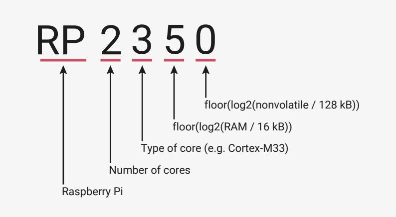
The diagram illustrates the naming convention for the RP2350 chip. The name is broken down into its components with arrows indicating their meaning:
- RP : Raspberry Pi
- 2 : Number of cores
- 3 : Type of core (e.g. Cortex-M33)
- 5 : \( \text{floor}(\log_2(\text{RAM} / 16 \text{ kB})) \)
- 0 : \( \text{floor}(\log_2(\text{nonvolatile} / 128 \text{ kB})) \)
The post-fix numeral on RP2350 comes from the following,
- 1. Number of processor cores
- ◦ 2 indicates a dual-core system
- 2. Loosely which type of processor
- ◦ 3 indicates Cortex-M33 or Hazard3
- 3. Internal memory capacity:
\(
\log_2 \lfloor \frac{\text{RAM}}{16 \text{ kB}} \rfloor
\)
- ◦ 5 indicates at least \( 2^5 \times 16 \text{ kB} = 512 \text{ kB} \)
- ◦ RP2350 has 520 kB of main system SRAM
- 4. Internal storage capacity: \( \log_2 \lfloor \frac{\text{nonvolatile}}{128 \text{ kB}} \rfloor \) (or 0 if no onboard nonvolatile storage)
- ◦ RP2350 uses external flash
- ◦ RP2354 has \( 2^4 \times 128 \text{ kB} = 2 \text{ MB} \) of internal flash
1.4. Version History
Table 7 lists versions of RP2350. Later versions fix bugs in earlier versions. For more information about the changes made between versions, see Appendix C . Also refer to Product Change Notification (PCN) 28.
Table 7. RP2350
version history
| Version | Use |
|---|---|
| A0 | Internal development |
| A1 | Internal development |
| A2 | Initial release |
| A3 | Internal development, samples, and limited production |
| A4 | Production version |