2. System bus
2.1. Bus fabric
The RP2350 bus fabric routes addresses and data across the chip.
Figure 5 shows the high-level structure of the bus fabric. The main AHB5 crossbar routes addresses and data between its 6 upstream ports and 17 downstream ports, with up to six bus transfers taking place each cycle. All data paths are 32 bits wide. Memories connect to multiple dedicated ports on the main crossbar, for the best possible memory bandwidth. High-bandwidth AHB peripherals share a port on the crossbar. An APB bridge provides access to system control registers and lower-bandwidth peripherals. The SIO peripherals are accessed via a dedicated path from each processor.
Figure 5. RP2350 bus fabric overview.
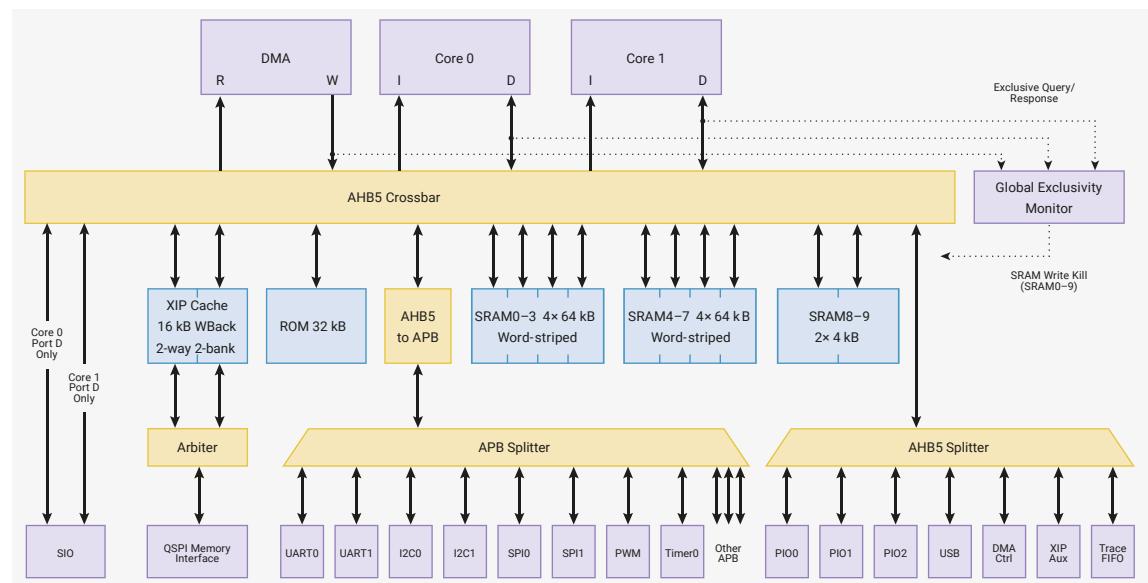
The bus fabric connects 6 AHB5 managers, i.e. bus ports which generate addresses:
- • Core 0: Instruction port (instruction fetch), and Data port (load/store access)
- • Core 1: Instruction port (instruction fetch), and Data port (load/store access)
- • DMA controller: Read port, Write port
The following 13 downstream ports are symmetrically accessible from all 6 upstream ports:
- • Boot ROM (1 port)
- • XIP (2 ports, striped)
- • SRAM (10 ports, striped)
Additionally, the following 2 ports are accessible for processor load/store and DMA read/write only:
- • 1 shared port for fast AHB5 peripherals: PIO0, PIO1, PIO2, USB, DMA control registers, XIP DMA FIFOs, HSTX FIFO, CoreSight trace DMA FIFO
- • 1 port for the APB bridge, to all APB peripherals and control registers
Instruction fetch from peripherals is physically disconnected , to avoid this IDAU-Exempt region ever becoming both Non-secure-writable and Secure-executable. This includes USB RAM, OTP and boot RAM. See Section 10.2.2 .
The SIO block, which was connected to the Cortex-M0+ IOPORT on RP2040, provides two AHB ports, each dedicated to load/store access from one core.
The six managers can access any six different crossbar ports simultaneously. So, at a system clock of 150 MHz, the maximum sustained bus bandwidth is 3.6 GB/s.
2.1.1. Bus priority
The main AHB5 crossbar implements a two-level bus priority scheme. Priority levels are configured separately for core 0, core 1, DMA read and DMA write, using the BUS_PRIORITY register in the BUSCTRL register block.
When a downstream subordinate receives multiple simultaneous access requests, the port serves high-priority (priority level 1) managers before serving any requests from low-priority (priority 0) managers. If all requests come from managers with the same priority level, the port applies a round-robin tie break, granting access to each manager in turn.
NOTEPriority arbitration only applies when multiple managers attempt to access the same subordinate on the same cycle. When multiple managers access different subordinates, e.g. different SRAM banks, the requests proceed simultaneously.
A subordinate with zero wait states can be accessed once per system clock cycle. When accessing a subordinate with zero wait states (e.g. SRAM), high-priority managers never experience delays caused by accesses from low-priority managers. This guarantees latency and throughput for real-time use cases. However, it also means that low-priority managers may stall until there is a free cycle.
2.1.2. Bus security filtering
Every point where the fabric connects to a downstream AHB or APB peripheral is interposed by a bus security filter, which enforces the following access control lists as defined by the ACCESSCTRL registers ( Section 10.6 ):
- • A list of who can access the port: core 0, core 1, DMA, debugger
- • A list of the security states from which the port can be accessed: the four combinations of Secure/Non-secure and Privileged/Unprivileged.
Accesses that fail either check are prevented from accessing the downstream port, and return a bus error upstream.
There are three exceptions, which do not implement bus security filters because they implement their own security filtering internally:
- • The ACCESSCTRL block itself, which is always world-readable, but filters writes on security and privilege
- • Boot RAM, which is hardwired to Secure access only
- • The single-cycle IO subsystem (SIO), which is internally banked over Secure and Non-secure
The Cortex-M Private Peripheral Bus (PPB) registers also lack ACCESSCTRL permissions because they are internal to the processors, not accessed through the system bus. The PPB registers are internally banked over Secure and Non-secure.
2.1.3. Atomic register access
Each peripheral register block is allocated 4 kB of address space, with registers accessed using one of 4 methods, selected by address decode.
- •
Addr + 0x0000: normal read write access - •
Addr + 0x1000: atomic XOR on write - •
Addr + 0x2000: atomic bitmask set on write - •
Addr + 0x3000: atomic bitmask clear on write
This allows software to modify individual fields of a control register without performing a read-modify-write sequence. Instead, the peripheral itself modifies its contents in-place. Without this capability, it is difficult to safely access IO registers when an interrupt service routine is concurrent with code running in the foreground, or when the two processors run code in parallel.
The four atomic access aliases occupy a total of 16 kB. Native atomic writes take the same number of clock cycles as normal writes. Most peripherals on RP2350 provide this functionality natively, but some peripherals (I2C, UART, SPI and SSI) add this functionality using a bus interposer. The bus interposer translates upstream atomic writes into downstream read-modify-write sequences at the boundary of the peripheral, at the cost of additional clock cycles. Atomic writes that use a bus interposer take two additional clock cycles compared to normal writes.
The following registers do not support atomic register access:
- • SIO ( Section 3.1 ), though some individual registers (for example, GPIO) have set, clear, and XOR aliases.
- • Any register accessed through the self-hosted CoreSight window, including Arm Mem-APs and the RISC-V Debug Module.
- • Standard Arm control registers on the Cortex-M33 private peripheral bus (PPB), except for Raspberry Pi-specific registers on the EPPB.
- • OTP programming registers accessed through the SBPI bridge.
2.1.4. APB bridge
The APB bridge provides an interface between the high-speed main AHB5 interconnect and the lower-bandwidth peripherals. Unlike the AHB5 fabric, which offers zero-wait-state accesses everywhere, APB accesses take a minimum of three cycles for a read, and four cycles for a write.
As a result, the throughput of the APB portion of the bus fabric is lower than the AHB5 portion. However, there is more than sufficient bandwidth to saturate the APB serial peripherals.
The following APB ports contain asynchronous bus crossings, which insert additional stall cycles on top of the typical cost of a read or write in the APB bridge:
- • ADC
- • HSTX_CTRL
- • OTP
- • POWMAN
The APB bridge implements a fixed timeout for stalled downstream transfers. The downstream bus may stall indefinitely, such as when accessing an asynchronous bus crossing when the destination clock is stopped, or deadlock conditions when accessing system APB registers through Mem-APs in the self-hosted debug window ( Section 3.5.6 ). When an APB transfer exceeds 65,535 cycles the APB bridge abandons the transfer and returns a bus fault. This keeps the system bus available so that software or the debugger can diagnose the reason for the overly long transfer.
2.1.5. Narrow IO register writes
The majority of memory-mapped IO registers on RP2350 ignore the width of bus read/write accesses. They treat all writes as though they were 32 bits in size. This means software cannot use byte or halfword writes to modify part of an IO register: any write to an address where the 30 address MSBs match the register address affects the contents of the entire register.
To update part of an IO register without a read-modify-write sequence, the best solution on RP2350 is atomic set/clear/XOR (see Section 2.1.3 ). This is more flexible than byte or halfword writes, as any combination of fields can be updated in one operation.
Upon a 8-bit or 16-bit write (such as a
strb
instruction on the Cortex-M33), the narrow value is replicated multiple times across the 32-bit data bus, so that it is broadcast to all 8-bit or 16-bit segments of the destination register:
Pico Examples: https://github.com/raspberrypi/pico-examples/blob/master/system/narrow_io_write/narrow_io_write.c Lines 19 - 62
19 int main() {
20     stdio_init_all();
21
22     // We'll use WATCHDOG_SCRATCH0 as a convenient 32 bit read/write register
23     // that we can assign arbitrary values to
24     io_rw_32 *scratch32 = &watchdog_hw->scratch[0];
25     // Alias the scratch register as two halfwords at offsets +0x0 and +0x2
26     volatile uint16_t *scratch16 = (volatile uint16_t *) scratch32;
27     // Alias the scratch register as four bytes at offsets +0x0, +0x1, +0x2, +0x3:
28     volatile uint8_t *scratch8 = (volatile uint8_t *) scratch32;
29
30     // Show that we can read/write the scratch register as normal:
31     printf("Writing 32 bit value\n");
32     *scratch32 = 0xdeadbeef;
33     printf("Should be 0xdeadbeef: 0x%08x\n", *scratch32);
34
35     // We can do narrow reads just fine -- IO registers treat this as a 32 bit
36     // read, and the processor/DMA will pick out the correct byte lanes based
37     // on transfer size and address LSBs
38     printf("\nReading back 1 byte at a time\n");
39     // Little-endian!
40     printf("Should be ef be ad de: %02x ", scratch8[0]);
41     printf("%02x ", scratch8[1]);
42     printf("%02x ", scratch8[2]);
43     printf("%02x\n", scratch8[3]);
44
45     // Byte writes are replicated four times across the 32-bit bus, and IO
46     // registers usually sample the entire write bus.
47     printf("\nWriting 8 bit value 0xa5 at offset 0\n");
48     scratch8[0] = 0xa5;
49     // Read back the whole scratch register in one go
50     printf("Should be 0xa5a5a5a5: 0x%08x\n", *scratch32);
51
52     // The IO register ignores the address LSBs [1:0] as well as the transfer
53     // size, so it doesn't matter what byte offset we use
54     printf("\nWriting 8 bit value at offset 1\n");
55     scratch8[1] = 0x3c;
56     printf("Should be 0x3c3c3c3c: 0x%08x\n", *scratch32);
57
58     // Halfword writes are also replicated across the write data bus
59     printf("\nWriting 16 bit value at offset 0\n");
60     scratch16[0] = 0xf00d;
61     printf("Should be 0xf00df00d: 0x%08x\n", *scratch32);
62 }
To disable this behaviour on RP2350, set bit 14 of the address by accessing the peripheral at an offset of
+0x4000
. This
causes invalid byte lanes to be driven to zero, rather than being driven with replicated data. In some situations, such as DMA of 8-bit values to the PWM peripheral, the default replication behaviour is not desirable.
2.1.6. Global Exclusive Monitor
The Global Exclusive Monitor enables standard Arm and RISC-V atomic instructions to safely access shared variables in SRAM from both cores. This underpins software libraries for manipulating shared variables, such as
stdatomic.h
in C11. For detailed rules governing the monitor's operation, see the
Armv8-M Architecture Reference Manual
.
Arm describes exclusive monitor interactions in terms of a processing element , PE, which performs a sequence of bus accesses. For RP2350 purposes, this is one AHB5 manager out of the following three: core 0 load/store, core 1 load/store, and DMA write. The DMA does not itself perform exclusive accesses, but its writes are monitored with respect to exclusive sequences on either processor. No distinction is made between debugger and non-debugger accesses from a processor.
The monitor observes all transfers on SRAM initiated by the DMA write and processor load/store ports, and pays particular attention to two types of transfer:
- • AHB5
exclusive reads
: Arm
ldrex*instructions, RISC-Vlr.winstructions, and the read phase of RISC-V AMOs (The Hazard3 cores on RP2350 implement AMOs as an exclusive read/write pair that retries until the write succeeds). - • AHB5
exclusive writes
: Arm
strex*instructions, RISC-Vsc.winstructions, and the writeback phase of RISC-V AMOs
Based on these observations, the monitor enforces that an atomic read-modify-write sequence (formed of an exclusive read followed by a successful exclusive write by the same PE) is not interleaved with another PE's successful write (exclusive or not) to the same reservation granule. A reservation granule is any 16-byte, naturally aligned area of SRAM. An exclusive write succeeds when all of the following are true:
- • It is preceded by an exclusive read by the same PE
- • No other exclusive writes were performed by this PE since that exclusive read
- • The exclusive read was to the same reservation granule
- • The exclusive read was of the same size (byte/halfword/word)
- • The exclusive read was from the same security and privilege state
- • No other PEs successfully wrote to the same granule since that exclusive read
If the above conditions are
not
met, the Global Exclusive Monitor shoots down the exclusive write before SRAM can commit the write data. The failure is reported to the originating PE, for example by a non-zero return value from an Arm
strex
instruction.
This implementation of the Armv8-M Global Exclusive Monitor also meets the requirements for RISC-V
lr/sc
and
amo*
instructions, with the caveat that the
RsrvEventual
PMA is not supported. (In practice, whilst it is quite easy to come up with contrived examples of starvation such as the DMA writing to a shared variable on every single cycle, bounded LR/SC and AMO sequences will generally complete quickly.)
 CAUTION
Secure software should avoid shared variables in Non-secure-accessible memory. Such variables are vulnerable to deliberate starvation from exclusive accesses by repeatedly performing non-exclusive writes.
Exclusive accesses are only supported on SRAM. The system treats exclusive accesses to other memory regions as normal reads and writes, reporting exclusivity failure to the originating PE, for example by a non-zero return value from an Arm
strex
instruction.
2.1.6.1. Implementation-defined monitor behaviour
The Armv8-M Architecture Reference Manual leaves several aspects of the Global Exclusive Monitor up to the implementation. For completeness, the RP2350 implementation defines them as follows:
- • The reservation granule size is fixed at 16 bytes
- • A single reservation is tracked per PE
- • The Arm
clrexinstruction does not affect global monitor state - • Any exclusive write by a PE clears that PE's global reservation
- • A non-exclusive write by a PE does not clear that PE's global reservation, no matter the address
Only the following updates a PE's reservation tag, setting its reservation state to Exclusive :
- • An exclusive read on SRAM
Only the following changes a PE's reservation state from Exclusive to Open :
- • A successful exclusive write from another PE to this PE's reservation
- • A non-exclusive write from another PE to this PE's reservation
- • Any exclusive write by this PE
- • An exclusive read by this PE, not on SRAM
A reservation granule can span multiple SRAM banks, so multiple operations on the same reservation granule may complete on the same cycle. This can result in the following problematic situations:
- • Multiple exclusive writes to the same reservation granule, reserved on each PE: in this case the lowest-numbered PE succeeds (in the order DMA < core 0 < core 1), and all others fail.
- • A mixture of non-exclusive and exclusive writes to the same reservation granule on the same cycle: in this case, the exclusive writes fail.
- • One PE x can write to a reservation granule on the same cycle that another PE y attempts to reserve the same reservation granule via exclusive load: in this case, y 's reservation is granted (i.e. the write takes place logically before the load).
- • One PE x can write to a reservation granule reserved by another PE y , on the same cycle that PE y makes a new reservation on a different reservation granule: in this case, again, y 's reservation is granted.
These rules can be summarised by a logical ordering of all possible events on a reservation granule that can occur on the same cycle: first all normal writes in arbitrary order, then all exclusive writes in ascending PE order (DMA, core 0, core 1), then all loads in arbitrary order.
2.1.6.2. Regions without exclusives support
The Global Exclusive monitor only supports exclusive transactions on certain address ranges. The main system SRAM supports exclusive transactions throughout its entire range:
0x20000000
through
0x20082000
. Within ranges that support exclusive transactions, the Global Exclusive monitor:
- • Tracks exclusive sequences across all participating PEs.
- • Drives the exclusive success/failure response correctly based on the observed ordering.
- • Shoots down failing exclusive writes so that they have no effect.
Exclusive transactions aren't supported outside of this range; all exclusive accesses report exclusive failure (both exclusive reads and exclusive writes), and exclusive writes aren't suppressed.
Outside of regions with exclusive transaction support, load/store exclusive loops run forever while still affecting SRAM contents. This applies to both Arm processors performing exclusive reads/writes and RISC-V processors performing
lr.w/sc.w
instructions. However, an
amo*.w
instruction on Hazard3 will result in a Store/AMO Fault, as the hardware
detects the failed exclusive read and bails out to avoid an infinite loop.
It is recommended not to perform exclusive accesses on regions outside of main SRAM. Shared variables outside of main SRAM can be protected using either lock variables in main SRAM, the SIO spinlocks, or a locking protocol that does not require exclusive accesses, such as a lock-free queue.
2.1.7. Bus performance counters
Bus performance counters automatically count accesses to the main AHB5 crossbar arbiters. These counters can help diagnose high-traffic performance issues.
There are four performance counters, starting at PERFCTR0 . Each is a 24-bit saturating counter. Counter values can be read from BUSCTRL_PERFCTR x and cleared by writing any value to BUSCTRL_PERFCTR x . Each counter can count one of the 20 available events at a time, as selected by BUSCTRL_PERFSEL x . For more information, see Section 12.15.4 .
2.2. Address map
The address map for the device is split into sections as shown in Table 8 . Details are shown in the following sections. Unmapped address ranges raise a bus error when accessed.
Each link in the left-hand column of Table 8 goes to a detailed address map for that address range. The detailed address maps have a link for each address to the relevant documentation for that address.
Rough address decode is first performed on bits 31:28 of the address:
Table 8. Address Map Summary
| Bus Segment | Base Address |
|---|---|
| ROM | 0x00000000 |
| XIP | 0x10000000 |
| SRAM | 0x20000000 |
| APB Peripherals | 0x40000000 |
| AHB Peripherals | 0x50000000 |
| Core-local Peripherals (SIO) | 0xd0000000 |
| Cortex-M33 private registers | 0xe0000000 |
2.2.1. ROM
ROM is accessible to DMA, processor load/store, and processor instruction fetch. It is located at address zero, which is the starting point for both Arm processors when the device is reset.
Table 9. Address map for ROM bus segment
| Bus Endpoint | Base Address |
|---|---|
| ROM_BASE | 0x00000000 |
2.2.2. XIP
XIP is accessible to DMA, processor load/store, and processor instruction fetch. This address range contains various mirrors of a 64 MB space which is mapped to external memory devices. On RP2350 the lower 32 MB is occupied by the QSPI Memory Interface (QMI), and the remainder is reserved. QMI controls are in the APB register section.
Table 10. Address map for XIP bus segment
| Bus Endpoint | Base Address |
|---|---|
| XIP_BASE | 0x10000000 |
| XIP_NOCACHE_NOALLOC_BASE | 0x14000000 |
| XIP_MAINTENANCE_BASE | 0x18000000 |
| XIP_NOCACHE_NOALLOC_NOTRANSLATE_BASE | 0x1c000000 |
NOTE
XIP_SRAM_BASE no longer exists as a separate address range. Cache-as-SRAM is now achieved by pinning cache lines within the cached XIP address space.
2.2.3. SRAM
SRAM is accessible to DMA, processor load/store, and processor instruction fetch.
SRAM0-3 and SRAM4-7 are always striped on bits 3:2 of the address:
Table 11. Address map for SRAM bus segment, SRAM0-7 (striped)
| Bus Endpoint | Base Address |
|---|---|
| SRAM_BASE | 0x20000000 |
| SRAM_STRIPED_BASE | 0x20000000 |
| SRAM0_BASE | 0x20000000 |
| SRAM4_BASE | 0x20040000 |
| SRAM_STRIPED_END | 0x20080000 |
There are two striped regions, each 256 kB in size, and each striped over 4 SRAM banks. SRAM0-3 are in the SRAM0 power domain, and SRAM4-7 are in the SRAM1 power domain.
SRAM 8-9 are always non-striped:
Table 12. Address map for SRAM bus segment, SRAM8-9 (non-striped)
| Bus Endpoint | Base Address |
|---|---|
| SRAM8_BASE | 0x20080000 |
| SRAM9_BASE | 0x20081000 |
| SRAM_END | 0x20082000 |
These smaller blocks of SRAM are useful for hoisting high-bandwidth data structures like the processor stacks. They are in the SRAM1 power domain.
2.2.4. APB registers
APB peripheral registers are accessible to processor load/store and DMA only. Instruction fetch will always fail.
The APB peripheral segment provides access to control and configuration registers, as well as data access for lower-bandwidth peripherals. APB writes cost a minimum of four cycles, and APB reads a minimum of three.
Table 13. Address map for APB bus segment
| Bus Endpoint | Base Address |
|---|---|
| SYSINFO_BASE | 0x40000000 |
| SYSCFG_BASE | 0x40080000 |
| Bus Endpoint | Base Address |
|---|---|
| CLOCKS_BASE | 0x40010000 |
| PSM_BASE | 0x40018000 |
| RESETS_BASE | 0x40020000 |
| IO_BANK0_BASE | 0x40028000 |
| IO_QSPI_BASE | 0x40030000 |
| PADS_BANK0_BASE | 0x40038000 |
| PADS_QSPI_BASE | 0x40040000 |
| XOSC_BASE | 0x40048000 |
| PLL_SYS_BASE | 0x40050000 |
| PLL_USB_BASE | 0x40058000 |
| ACCESSCTRL_BASE | 0x40060000 |
| BUSCTRL_BASE | 0x40068000 |
| UART0_BASE | 0x40070000 |
| UART1_BASE | 0x40078000 |
| SPI0_BASE | 0x40080000 |
| SPI1_BASE | 0x40088000 |
| I2C0_BASE | 0x40090000 |
| I2C1_BASE | 0x40098000 |
| ADC_BASE | 0x400a0000 |
| PWM_BASE | 0x400a8000 |
| TIMER0_BASE | 0x400b0000 |
| TIMER1_BASE | 0x400b8000 |
| HSTX_CTRL_BASE | 0x400c0000 |
| XIP_CTRL_BASE | 0x400c8000 |
| XIP_QMI_BASE | 0x400d0000 |
| WATCHDOG_BASE | 0x400d8000 |
| BOOTRAM_BASE | 0x400e0000 |
| ROSC_BASE | 0x400e8000 |
| TRNG_BASE | 0x400f0000 |
| SHA256_BASE | 0x400f8000 |
| POWMAN_BASE | 0x40100000 |
| TICKS_BASE | 0x40108000 |
| OTP_BASE | 0x40120000 |
| OTP_DATA_BASE | 0x40130000 |
| OTP_DATA_RAW_BASE | 0x40134000 |
| OTP_DATA_GUARDED_BASE | 0x40138000 |
| Bus Endpoint | Base Address |
|---|---|
| OTP_DATA_RAW_GUARDED_BASE | 0x4013c000 |
| CORESIGHT_PERIPH_BASE | 0x40140000 |
| CORESIGHT_ROMTABLE_BASE | 0x40140000 |
| CORESIGHT_AHB_AP_CORE0_BASE | 0x40142000 |
| CORESIGHT_AHB_AP_CORE1_BASE | 0x40144000 |
| CORESIGHT_TIMESTAMP_GEN_BASE | 0x40146000 |
| CORESIGHT_ATB_FUNNEL_BASE | 0x40147000 |
| CORESIGHT_TPIU_BASE | 0x40148000 |
| CORESIGHT_CTL_BASE | 0x40149000 |
| CORESIGHT_APB_AP_RISCV_BASE | 0x4014a000 |
| GLITCH_DETECTOR_BASE | 0x40158000 |
| TBMAN_BASE | 0x40160000 |
2.2.5. AHB registers
AHB peripheral registers are accessible to processor load/store and DMA only. Instruction fetch will always fail.
The AHB peripheral segment provides access to higher-bandwidth peripherals. The minimum read/write cost is one cycle, and peripherals may insert up to one wait state.
Table 14. Address map for AHB peripheral bus segment
| Bus Endpoint | Base Address |
|---|---|
| DMA_BASE | 0x50000000 |
| USBCTRL_BASE | 0x50100000 |
| USBCTRL_DPRAM_BASE | 0x50100000 |
| USBCTRL_REGS_BASE | 0x50110000 |
| PIO0_BASE | 0x50200000 |
| PIO1_BASE | 0x50300000 |
| PIO2_BASE | 0x50400000 |
| XIP_AUX_BASE | 0x50500000 |
| HSTX_FIFO_BASE | 0x50600000 |
| CORESIGHT_TRACE_BASE | 0x50700000 |
2.2.6. Core-local peripherals (SIO)
SIO is accessible to processor load/store only. It contains registers which need single-cycle access from both cores concurrently, such as the GPIO registers. Access is always zero-wait-state.
Table 15. Address map for SIO bus segment
| Bus Endpoint | Base Address |
|---|---|
| SIO_BASE | 0xd0000000 |
| SIO_NONSEC_BASE | 0xd0020000 |
2.2.7. Cortex-M33 private peripherals
The PPB is accessible to processor load/store only.
The PPB region contains standard control registers defined by Arm, Non-secure aliases of some of those registers, and a handful of other core-local registers defined by Raspberry Pi (the EPPB).
These addresses are only accessible to Arm processors: RISC-V processors will return a bus fault.
Table 16. Address map for PPB bus segment
| Bus Endpoint | Base Address |
|---|---|
| PPB_BASE | 0xe0000000 |
| PPB_NONSEC_BASE | 0xe0020000 |
| EPPB_BASE | 0xe0080000 |