3. Processor subsystem
Figure 6. The RP2350 processor subsystem connects two processors to the system bus, peripheral interrupts, GPIOs, and a Serial Wire Debug (SWD) connection from an external debug host. It also contains closely-coupled peripherals, and peripherals used for synchronisation and communication, which are collectively referred to as the single-cycle IO subsystem (SIO).
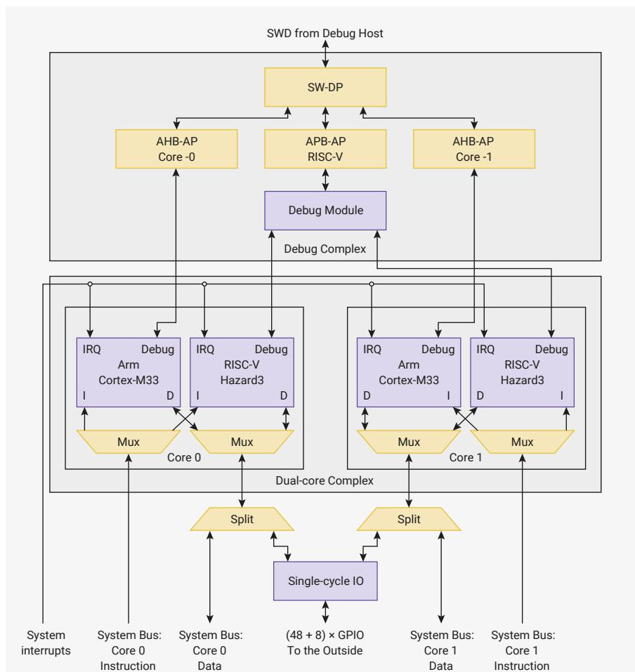
The diagram illustrates the RP2350 processor subsystem architecture. At the top, a 'SWD from Debug Host' connects to a 'SW-DP' block. The 'SW-DP' is connected to three blocks: 'AHB-AP Core -0', 'APB-AP RISC-V', and 'AHB-AP Core -1'. These three blocks are connected to a 'Debug Module', which is part of a 'Debug Complex'. The 'Debug Complex' is connected to the 'Dual-core Complex'. The 'Dual-core Complex' contains two identical core blocks, 'Core 0' and 'Core 1'. Each core block contains an 'IRQ' block, an 'Arm Cortex-M33' block, a 'Debug' block, and a 'RISC-V Hazard3' block. These are connected to a 'Mux' (multiplexer) block. The 'Mux' blocks are connected to a 'Split' block, which is connected to a 'Single-cycle IO' block. The 'Single-cycle IO' block is connected to the 'System Bus' for both 'Core 0' and 'Core 1'. The 'System Bus' for 'Core 0' is connected to 'System interrupts', 'System Bus: Core 0 Instruction', and 'System Bus: Core 0 Data'. The 'System Bus' for 'Core 1' is connected to 'System Bus: Core 1 Data' and 'System Bus: Core 1 Instruction'. The 'Single-cycle IO' block is also connected to '(48 + 8) x GPIO To the Outside'.
RP2350 is a symmetric dual-core system. Two cores operate simultaneously and independently, offering high processing throughput and the ability to route interrupts to different cores to improve throughput and latency of interrupt handling. The two cores have a symmetric view of the system bus; all memory resources on RP2350 are accessible equally on both cores, with the same performance.
Each core has a pair of 32-bit AHB5 links to the system bus. One is used exclusively for instruction fetch, the other exclusively for load or store instructions and debugger access. Each core can perform one instruction fetch and one load or store access per cycle, provided there are no conflicts on the downstream bus ports.
There are two sockets for cores to attach to the system bus, referred to as core 0 and core 1 throughout this datasheet. (They may synonymously be referred to as core0, core1, proc0 and proc1 in register documentation.) The processor plugged into each socket is selectable at boot time:
- • A Cortex-M33 processor, implementing the Armv8-M Main instruction set, plus extensions
- • A Hazard3 processor, implementing the RV32IMAC instruction set, plus extensions
Cortex-M33 is the default option. Whichever processor is unused is held in reset with its clock gated at the top level. Unused processors use zero dynamic power. See Section 3.9 for information about the architecture selection hardware.
The two Cortex-M33 instances are identical. They are configured with the Security, DSP and FPU extensions, as well as 8x SAU regions, 8x Secure MPU regions and 8x Non-secure MPU regions. Section 3.7 documents the Cortex-M33 processor as well as the specific configuration used on RP2350. The two Hazard3 instances are also identical to one another; see Section 3.8 for the features and operation of the Hazard3 processors.
The Cortex-M33 implementation of the Armv8-M Security extension (also known as TrustZone-M) isolates trusted and untrusted software running on-device. RP2350 extends the strict partitioning of the Arm Secure and Non-secure states throughout the system, including the ability to assign peripherals, GPIOs and DMA channels to each security domain. See Section 10.2 for a high-level overview of Armv8-M Security extension features in the context of the RP2350 security architecture.
Not shown on Figure 6 are the coprocessors for the Cortex-M33. These are closely coupled to the core, offering a transfer rate of 64 bits per cycle in and out of the Arm register file. You may consider them to be inside the Cortex-M33 block on the diagram. RP2350 equips each Cortex-M33 with the following coprocessors:
- • Coprocessor 0 : GPIO coprocessor (GPIOC), described in Section 3.6.1
- • Coprocessors 4 and 5 : Secure and Non-secure instances of the double-precision coprocessor (DCP), described in Section 3.6.2
- • Coprocessor 7 : redundancy coprocessor (RCP), described in Section 3.6.3
An external debug host can access both cores over a Serial Wire Debug (SWD) bus. The host can:
- • run, halt and reset the cores
- • inspect internal core state such as registers
- • access memory from the core's point of view
- • load code onto the device and run it
Section 3.5 describes the debug hardware in addition to the instruction trace hardware available on the Arm processors.
Peripherals throughout the system assert interrupt requests (IRQs) to demand attention from the processors. For example, a UART peripheral asserts its interrupt when it has received a character, so the processor can collect it from the receive FIFO. All interrupts route to both cores, and the core's internal interrupt controller selects the interrupt signals it wishes to subscribe to. Section 3.2 defines the system-level IRQ numbering as well as details of the Arm non-maskable interrupt (NMI).
The event signals described in Section 3.3 are a mechanism for processors to sleep when waiting for other processors in the system to complete a task or free up some resource. Each processor sees events emitted by the other processor. They also see exclusivity events generated by the Global Exclusive Monitor described in Section 2.1.6 , which is the piece of hardware that allows the processors to safely manipulate shared variables using atomic read-modify-write sequences.
3.1. SIO
The Single-cycle IO subsystem (SIO) contains peripherals that require low-latency, deterministic access from the processors. It is accessed via the AHB Fabric. The SIO has a dedicated bus interface for each processor, as shown in Figure 7 .
Figure 7. The single-cycle IO block contains registers which processors must access quickly. FIFOs, doorbells and spinlocks support message passing and synchronisation between the two cores. The shared GPIO registers provide fast, direct access to GPIO-capable pins. Interpolators can accelerate common software tasks. Most SIO hardware is banked (duplicated) for Secure and Non-secure access. Grey arrows show bus connections for Non-secure access.
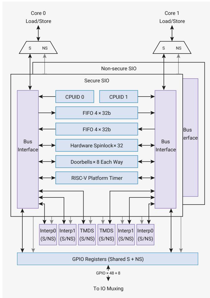
The SIO contains:
- • CPUID registers which read as 0/1 on core 0/1 ( Section 3.1.2 )
- • Mailbox FIFOs for passing ordered messages between cores ( Section 3.1.5 )
- • Doorbells for interrupting the opposite core on cumulative and unordered events ( Section 3.1.6 )
- • Hardware spinlocks for implementing critical sections without using exclusive bus accesses ( Section 3.1.4 )
- • Interpolators ( Section 3.1.10 ) and TMDS encoders ( Section 3.1.9 )
- • Standard RISC-V 64-bit platform timer ( Section 3.1.8 ) which is usable by both Arm and RISC-V software
- • GPIO registers for fast software bitbanging ( Section 3.1.3 ), with shared access from both cores
Most SIO hardware is duplicated for Secure/Non-secure access. Non-secure access to the FIFO registers will see a physically different FIFO than Secure access to the same address, so that messages belonging to Secure and Non-secure software are not mixed: Section 3.1.1 describes this Secure/Non-secure banking in more detail.
3.1.1. Secure and Non-secure SIO
To allow isolation of Secure and Non-secure software, whilst keeping a consistent programming model for software written to run in either domain, the SIO is duplicated into a Secure and a Non-secure bank. Most hardware is duplicated between the two banks, including:
- • Mailbox FIFOs
- • Doorbell registers
- • Interrupt outputs to processors
- • Spinlocks
For example, Non-secure code on core 0 can pass messages to Non-secure code on core 1 through the Non-secure instance of the mailbox FIFO. In turn, this message will generate a Non-secure interrupt, which is separate from the Secure FIFO interrupt line. This does not interfere with any Secure message passing that might be going on at the same time, and Non-secure code can not snoop Secure messages because it does not have access to the Secure mailboxes. The software running in the Secure and Non-secure domain can be identical, and the processors' bus accesses to the SIO will automatically be routed to the Secure or Non-secure version of the mailbox registers.
The following hardware is not duplicated:
- • The GPIO registers are shared, and Non-secure accesses are filtered on a per-GPIO basis by the Non-secure GPIO mask defined in the ACCESSCTRL GPIO_NSMASK0 and GPIO_NSMASK1 registers
- • The RISC-V standard platform timer ( MTIME , MTIMEH ), which is also usable by Arm processors, is present only in the Secure SIO, as it is a Machine-mode peripheral on RISC-V
- • The interpolator and TMDS encoder peripherals are assignable to either the Secure or Non-secure SIO using the PERL_NONSEC register
Accesses to the SIO register address range, starting at 0xd0000000 ( SIO_BASE ), are mapped to the SIO bank which matches the security attribute of the bus access. This means accesses from the Arm Secure state, or RISC-V Machine mode, will access the Secure SIO bank, and accesses from the Arm Non-secure state, or RISC-V User mode, will access the Non-secure SIO bank.
Additionally, Secure accesses can use the mirrored address range starting at 0xd0020000 ( SIO_NONSEC_BASE ) to access the Non-secure view of SIO, for example, using the Non-secure doorbells to interrupt Non-secure code running on the other core. Attempting to access this address range from Non-secure code will generate a bus fault.
i NOTE
The 0x20000 offset of the Secure-to-Non-secure mirror matches the PPB mirrors at 0xe0000000 ( PPB_BASE ) and 0xe0020000 ( PPB_NONSEC_BASE ), which function similarly.
i NOTE
Debug access is mapped to the Secure/Non-secure SIO using the security attribute of the debugger's bus access, which may differ from the security state that the core was halted in.
3.1.2. CPUID
The CPUID SIO register returns a value of 0 when read by core 0, and 1 when read by core 1. This helps software identify the core running the current application. The initial boot sequence also relies on this check: both cores start running simultaneously, core 1 goes into a deep sleep state, and core 0 continues the main boot sequence.
i IMPORTANT
Don't confuse the SIO CPUID register with the Cortex-M33 CPUID register on each processor's internal Private Peripheral Bus, which lists the processor's part number and version.
NOTEReading the MHARTID CSR on each Hazard3 core returns the same values as CPUID : 0 on core 0, and 1 on core 1.
3.1.3. GPIO control
The SIO GPIO registers control GPIOs which have the SIO function selected (function 5). This function is supported on the following pins:
- • All user GPIOs (GPIOs 0 through 29, or 0 through 47, depending on package option)
- • QSPI pins
- • USB DP/DM pins
All SIO GPIO control registers come in pairs. The lower-addressed register in each pair (for example, GPIO_IN ) is connected to GPIOs 0 through 31, and the higher-addressed register in each pair (for example, GPIO_HI_IN ) is connected to GPIOs 32 through 47, the QSPI pins, and the USB DP/DM pins.
NOTETo drive a pin with the SIO's GPIO registers, the GPIO multiplexer for this pin must first be configured to select the SIO GPIO function. See Table 646 .
These GPIO registers are shared between the two cores: both cores can access them simultaneously. There are three groups of registers:
- • Output registers, GPIO_OUT and GPIO_HI_OUT set the output level of the GPIO. 0 for low output, 1 for high output.
- • Output enable registers, GPIO_OE and GPIO_HI_OE , are used to enable the output driver. 0 for high-impedance, 1 for drive high or low based on GPIO_OUT and GPIO_HI_OUT .
- • Input registers, GPIO_IN and GPIO_HI_IN , allow the processor to sample the current state of the GPIOs.
Reading GPIO_IN returns up to 32 input values in a single read, and software then masks out individual pins it is interested in.
SDK: https://github.com/raspberrypi/pico-sdk/blob/master/src/rp2_common/hardware_gpio/include/hardware/gpio.h Lines 869 - 879
869 static inline bool gpio_get(uint gpio) {
870     #ifdef NUM_BANK0_GPIOS <= 32
871         return sio_hw->gpio_in & (1u << gpio);
872     #else
873         if (gpio < 32) {
874             return sio_hw->gpio_in & (1u << gpio);
875         } else {
876             return sio_hw->gpio_hi_in & (1u << (gpio - 32));
877         }
878     #endif
879 }
The OUT and OE registers also have atomic SET , CLR , and XOR aliases. This allows software to update a subset of the pins in one operation. This ensures safety for concurrent GPIO access, both between the two cores and between a single core's interrupt handler and foreground code.
SDK: https://github.com/raspberrypi/pico-sdk/blob/master/src/rp2_common/hardware_gpio/include/hardware/gpio.h Lines 918 - 924
918 static inline void gpio_set_mask(uint32_t mask) {
919     #ifdef PICO_USE_GPIO_COPROCESSOR
920         gpior_lo_out_set(mask);
921 #else 922 sio_hw->gpio_set = mask; 923 #endif 924 }
SDK: https://github.com/raspberrypi/pico-sdk/blob/master/src/rp2_common/hardware_gpio/include/hardware/gpio.h Lines 965 - 971
965 static inline void gpio_clr_mask(uint32_t mask) {
966 #ifdef PICO_USE_GPIO_COPROCESSOR
967     gpioc_lo_out_clr(mask);
968 #else
969     sio_hw->gpio_clr = mask;
970 #endif
971 }
SDK: https://github.com/raspberrypi/pico-sdk/blob/master/src/rp2_common/hardware_gpio/include/hardware/gpio.h Lines 1155 - 1180
1155 static inline void gpio_put(uint gpio, bool value) {
1156 #ifdef PICO_USE_GPIO_COPROCESSOR
1157     gpioc_bit_out_put(gpio, value);
1158 #elif NUM_BANK0_GPIOS <= 32
1159     uint32_t mask = 1ul << gpio;
1160     if (value)
1161         gpio_set_mask(mask);
1162     else
1163         gpio_clr_mask(mask);
1164 #else
1165     uint32_t mask = 1ul << (gpio & 0x1fu);
1166     if (gpio < 32) {
1167         if (value) {
1168             sio_hw->gpio_set = mask;
1169         } else {
1170             sio_hw->gpio_clr = mask;
1171         }
1172     } else {
1173         if (value) {
1174             sio_hw->gpio_hi_set = mask;
1175         } else {
1176             sio_hw->gpio_hi_clr = mask;
1177         }
1178     }
1179 #endif
1180 }
If both processors write to an OUT or OE register (or any of its SET/CLR/XOR aliases) on the same clock cycle, the result is as though core 0 wrote first, then core 1 wrote immediately afterward. For example, if core 0 SETs a bit and core 1 XORs it on the same clock cycle, the bit ends up with a value of 0 .
NOTEThis is a conceptual model for the result produced when two cores write to a GPIO register simultaneously. The register never contains the intermediate values at any point. In the previous example, if the pin is initially 0, and core 0 performs a SET while core 1 performs a XOR , the GPIO output remains low throughout the clock cycle.
As well as being shared between cores, the GPIO registers are also shared between security domains. The Secure and Non-secure SIO offer alternative views of the same GPIO registers, which are always mapped as GPIO function 5. However, the Non-secure SIO can only access pins which are enabled in the GPIO Non-secure mask configured by the ACCESSCTRL registers GPIO_NSMASK0 and GPIO_NSMASK1 . The layout of the NSMASK registers matches the layout of the SIO registers – for example, QSPI_SCK is bit 26 in both GPIO_HI_IN and GPIO_NSMASK1 .
When a pin is not enabled in Non-secure code:
- • Writes to the corresponding GPIO registers from a Non-secure context have no effect.
- • Reads from a Non-secure context return zeroes.
- • Reads and writes from a Secure context function as usual using the Secure bank.
The GPIO coprocessor port ( Section 3.6.1 ) provides dedicated instructions for accessing the SIO GPIO registers from the Cortex-M33 processors. This includes the ability to read and write 64 bits in a single operation.
3.1.4. Hardware spinlocks
The SIO provides 32 hardware spinlocks, which can be used to manage mutually-exclusive access to shared software resources. Each spinlock is a one-bit flag, mapped to a different address (from SPINLOCK0 to SPINLOCK31 ). Software interacts with each spinlock with one of the following operations:
- • Read: Attempt to claim the lock. Read value is non-zero if the lock was successfully claimed, or zero if the lock had already been claimed by a previous read.
- • Write (any value): Release the lock. The next attempt to claim the lock will succeed.
If both cores try to claim the same lock on the same clock cycle, core 0 succeeds.
Generally software will acquire a lock by repeatedly polling the lock bit ("spinning" on the lock) until it is successfully claimed. This is inefficient if the lock is held for long periods, so generally the spinlocks should be used to protect short critical sections of higher-level primitives such as mutexes, semaphores and queues.
For debugging purposes, the current state of all 32 spinlocks can be observed via SPINLOCK_ST .
NOTERP2350 has separate spinlocks for Secure and Non-secure SIO banks because sharing these registers would allow Non-secure code to deliberately starve Secure code that attempts to acquire a lock. See Section 3.1.1 .
NOTEThe processors on RP2350 support standard atomic/exclusive access instructions which, in concert with the global exclusive monitor ( Section 2.1.6 ), allow both cores to safely share variables in SRAM. The SIO spinlocks are still included for compatibility with RP2040.
NOTEDue to
RP2350-E2
, writes to new SIO registers above an offset of
+0x180
alias the spinlocks, causing spurious lock releases. The SDK by default uses atomic memory accesses to implement the
hardware_sync_spin_lock
API, as a workaround on RP2350 A2.
3.1.5. Inter-processor FIFOs (Mailboxes)
The SIO contains two FIFOs for passing data, messages or ordered events between the two cores. Each FIFO is 32 bits wide and four entries deep. One of the FIFOs can only be written by core 0 and read by core 1. The other can only be written by core 1 and read by core 0.
Each core writes to its outgoing FIFO by writing to
FIFO_WR
and reads from its incoming FIFO by reading from
FIFO_RD
. A status register,
FIFO_ST
, provides the following status signals:
- • Incoming FIFO contains data (
VLD). - • Outgoing FIFO has room for more data (
RDY). - • The incoming FIFO was read from while empty at some point in the past (
ROE). - • The outgoing FIFO was written to while full at some point in the past (
WOF).
Writing to the outgoing FIFO while full, or reading from the incoming FIFO while empty, does not affect the FIFO state. The current contents and level of the FIFO is preserved. However, this does represent some loss of data or reception of invalid data by the software accessing the FIFO, so a sticky error flag is raised (
ROE
or
WOF
).
The SIO has a FIFO IRQ output for each core to notify the core that it has received FIFO data. This is a
core-local interrupt
, mapped to the same IRQ number on each core (
SIO_IRQ_FIFO
, interrupt number 25). Non-secure FIFO interrupts use a separate interrupt line, (
SIO_IRQ_FIFO_NS
, interrupt number 27). It is not possible to interrupt on the opposite core's FIFO.
Each IRQ output is the logical OR of the
VLD
,
ROE
and
WOF
bits in that core's
FIFO_ST
register: that is, the IRQ is asserted if any of these three bits is high, and clears again when they are all low. To clear the
ROE
and
WOF
flags, write any value to
FIFO_ST
. To clear the
VLD
flag, read data from the FIFO until it is empty.
If the corresponding interrupt line is enabled in the processor's interrupt controller, the processor takes an interrupt each time data appears in its FIFO, or if it has performed some invalid FIFO operation (read on empty, write on full).
NOTEROE
and
WOF
only become set if software misbehaves in some way. Generally, the interrupt handler triggers when data appears in the FIFO, raising the
VLD
flag. Then, the interrupt handler clears the IRQ by reading data from the FIFO until
VLD
goes low once more.
The inter-processor FIFOs and the Event signals are used by the bootrom (
Chapter 5
)
wait_for_vector
routine, where core 1 remains in a sleep state until it is woken, and provided with its initial stack pointer, entry point and vector table through the FIFO.
RP2350 has separate FIFOs and interrupts for Secure and Non-secure SIO banks. See Section 3.1.1
3.1.6. Doorbells
The doorbell registers raise an interrupt on the opposite core. There are 8 doorbell flags in each direction, combined into a single doorbell interrupt per core. This is a core-local interrupt: the same interrupt number on each core (
SIO_IRQ_BELL
, interrupt number 26) notifies that core of incoming doorbell interrupts.
Whereas the mailbox FIFOs are used for cross-core events whose count and order is important, doorbells are used for events which are accumulative (i.e. may post multiple times, but only answered once) and which can be responded to in any order.
Writing a non-zero value to the
DOORBELL_OUT_SET
register raises the opposite core's doorbell interrupt. The interrupt remains raised until all bits are cleared. Generally, the opposite core enters its doorbell interrupt handler, reads its
DOORBELL_IN_CLR
register to get the mask of active doorbell flags, and then writes back to acknowledge and clear the interrupt.
The
DOORBELL_IN_SET
register allows a processor to ring its own doorbell. This is useful when the routine which rings a doorbell can be scheduled on either core. Likewise, for symmetry, a processor can clear the opposite core's doorbell flags using the
DOORBELL_OUT_CLR
register: this is useful for setup code, but should be avoided in general because of the potential for race conditions when acknowledging interrupts meant for the opposite core.
At any time, a core can read back its
DOORBELL_OUT_SET
or
DOORBELL_OUT_CLR
register (they return the same result) to see the status of doorbell interrupts posted to the opposite core. Likewise, reading either
DOORBELL_IN_SET
or
DOORBELL_IN_CLR
returns the status of doorbell interrupts posted to this core.
i NOTE
RP2350 has separate per-core doorbell interrupt signals and doorbell registers for Secure and Non-secure SIO banks. Non-secure doorbells are posted on
SIO_IRQ_BELL_NS
, interrupt number 28. See
Section 3.1.1
.
3.1.7. Integer divider
RP2040's memory-mapped integer divider peripheral is not present on RP2350, since the processors support divide instructions. The address space previously allocated for the divider registers is now reserved.
3.1.8. RISC-V platform timer
This 64-bit timer is a standard peripheral described in the RISC-V privileged specification, usable equally by the Arm and RISC-V processors on RP2350. It drives the per-core
SIO_IRQ_MTIMECMP
system-level interrupt (
Section 3.2
), as well as the
mip.mtip
timer interrupt on the RISC-V processors.
There is a single 64-bit counter, shared between both cores. The low and high half can be accessed through the
MTIME
and
MTIMEH
SIO registers. Use the following procedure to safely read the 64-bit time using 32-bit register accesses:
- 1. Read the upper half,
MTIMEH. - 2. Read the lower half,
MTIME. - 3. Read the upper half again.
- 4. Loop if the two upper-half reads returned different values.
This is similar to the procedure for reading RP2350 system timers ( Section 12.8 ). The loop should only happen once, when the timer is read at exactly the instant of a 32-bit rollover, and even this is only occasional. If you require constant-time operation, you can instead zero the lower half when the two upper-half reads differ.
Timer interrupts are generated based on a per-core 64-bit time comparison value, accessed through the
MTIMECMP
and
MTIMECMPH
SIO registers. Each core gets its own copy of these registers, accessed at the same address. The per-core interrupt is asserted whenever the current time indicated in the
MTIME
registers is greater than or equal to that core's
MTIMECMP
. Use the following sequence to write a new 64-bit timer comparison value without causing spurious interrupts:
- 1. Write all-ones to
MTIMECMP(guaranteed greater than or equal to the old value, and the lower half of the target value). - 2. Write the upper half of the target value to
MTIMECMPH(combined 64-bit value is still greater than or equal to the target value).
- 3. Write the lower half of the target value to MTIMECMP .
The RISC-V timer can count either ticks from the system-level tick generator ( Section 8.5 ), or system clock cycles, selected by the MTIME_CTRL register. Use a 1 microsecond time base for compatibility with most RISC-V software.
3.1.9. TMDS encoder
Each core is equipped with an implementation of the TMDS encode algorithm described in chapter 3 of the DVI 1.0 specification. In general, the HSTX peripheral ( Section 12.11 ) supports lower processor overhead for DVI-D output as well as a wider range of pixel formats, but the SIO TMDS encoders are included for use with non-HSTX-capable GPIOs.
The TMDS_CTRL register allows configuration of a number of input pixel formats, from 16-bit RGB down to 1-bit monochrome. Once the encoder has been set up, the processor writes 32 bits of colour data at a time to TMDS_WDATA , and then reads TMDS data symbols from the output registers. Depending on the pixel format, there may be multiple TMDS symbols read for each write to TMDS_WDATA . There are no stalls: encoding is limited entirely by the processor's load/store bandwidth, up to one 32-bit read or write per cycle per core.
To allow for framebuffer/scanbuffer resolution lower than the display resolution, the output registers have both peek and pop aliases (e.g. TMDS_PEEK_SINGLE and TMDS_POP_SINGLE ). Reading either register advances the encoder's DC balance counter, but only the pop alias shifts the colour data in TMDS_WDATA so that multiple correctly-DC-balanced TMDS symbols can be generated from the same input pixel.
The TMDS encoder peripherals are not duplicated over security domains. They are assigned to the Secure SIO at reset, and can be reassigned to the Non-secure SIO using the PERL_NONSEC register.
3.1.10. Interpolator
Each core is equipped with two interpolators ( INTERP0 and INTERP1 ) that can accelerate tasks by combining certain pre-configured operations into a single processor cycle. Intended for cases where the pre-configured operation repeats many times, interpolators result in code which uses both fewer CPU cycles and fewer CPU registers in time-critical sections.
The interpolators already accelerate audio operations within the SDK. Their flexible configuration makes it possible to optimise many other tasks, including:
- • quantization
- • dithering
- • table lookup address generation
- • affine texture mapping
- • decompression
- • linear feedback
Figure 8. An interpolator. The two accumulator registers and three base registers have single-cycle read/write access from the processor. The interpolator is organised into two lanes, which perform masking, shifting and sign-extension operations on the two accumulators. This produces three possible results, by adding the intermediate shift/mask values to the three base registers. From left to right, the multiplexers on each lane are controlled by the following flags in the CTRL registers: CROSS_RESULT , CROSS_INPUT , SIGNED , and ADD_RAW .
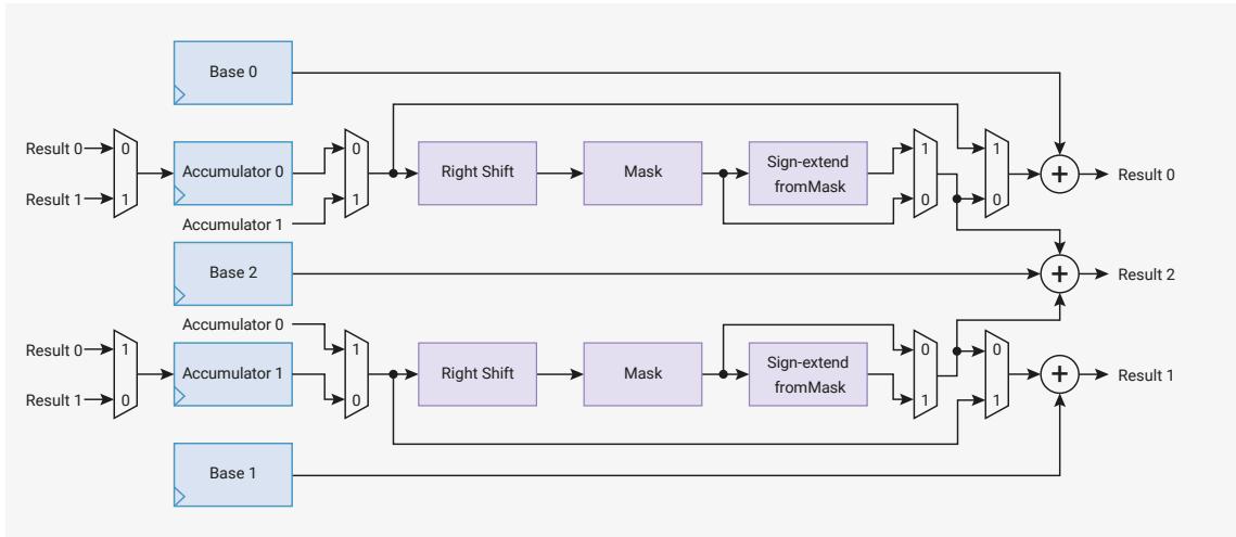
The processor can write or read any interpolator register in one cycle, and the results are ready on the next cycle. The processor can also perform an addition on one of the two accumulators ACCUM0 or ACCUM1 by writing to the corresponding ACCUMx_ADD register.
The three results are available in the read-only locations PEEK0 , PEEK1 , PEEK2 . Reading from these locations does not change the state of the interpolator. The results are also aliased at the locations POP0 , POP1 , POP2 ; reading from a POPx alias returns the same result as the corresponding PEEKx , and simultaneously writes back the lane results to the accumulators. Use the POPx aliases to advance the state of interpolator each time a result is read.
You can adjust interpolator behaviour with the following operational modes:
- • fractional blending between two values
- • clamping values to restrict them within a given range.
The following example shows a trivial example of popping a lane result to produce simple iterative feedback.
Pico Examples: https://github.com/raspberrypi/pico-examples/blob/master/interp/hello_interp/hello_interp.c Lines 11 - 23
11 void times_table() {
12     puts("9 times table:");
13
14     // Initialise lane 0 on interp0 on this core
15     interp_config cfg = interp_default_config();
16     interp_set_config(interp0, 0, &cfg);
17
18     interp0->accum[0] = 0;
19     interp0->base[0] = 9;
20
21     for (int i = 0; i < 10; ++i)
22         printf("%d\n", interp0->pop[0]);
23 }
3.1.10.1. Lane operations
Figure 9. Each lane of each interpolator can be configured to perform mask, shift and sign-extension on one of the accumulators. This is fed into adders which produce final results, which may optionally be fed back into the accumulators with each read. The datapath can be configured using a handful of 32-bit multiplexers. From left to right, these are controlled by the following CTRL flags: CROSS_RESULT, CROSS_INPUT, SIGNED, and ADD_RAW.

Each lane performs these three operations, in sequence:
- • A right shift by
CTRL_LANE
x
_SHIFT
(0 to 31 bits) - • A mask of bits from
CTRL_LANE x _MASK_LSBtoCTRL_LANE x _MASK_MSBinclusive (each ranging from bit 0 to bit 31) - • A sign extension from the top of the mask, i.e. take bit
CTRL_LANE x _MASK_MSBand OR it into all more-significant bits, ifCTRL_LANE x _SIGNEDis set
For example, if:
- •
ACCUM0 = 0xdeadbeef - •
CTRL_LANE0_SHIFT = 8 - •
CTRL_LANE0_MASK_LSB = 4 - •
CTRL_LANE0_MASK_MSB = 7 - •
CTRL_SIGNED = 1
Then lane 0 would produce the following results at each stage:
- • Right shift by 8 to produce
0x00deadbe - • Mask bits 7 to 4 to produce
0x00deadbe & 0x000000f0 = 0x000000b0 - • Sign-extend up from bit 7 to produce
0xffffffb0
In software:
Pico Examples: https://github.com/raspberrypi/pico-examples/blob/master/interp/hello_interp/hello_interp.c Lines 25 - 46
25 void moving_mask() {
26     interp_config cfg = interp_default_config();
27     interp0->accum[0] = 0x1234abcd;
28
29     puts("Masking:");
30     printf("ACCUM0 = %08x\n", interp0->accum[0]);
31     for (int i = 0; i < 8; ++i) {
32         // LSB, then MSB. These are inclusive, so 0,31 means "the entire 32 bit register"
33         interp_config_set_mask(&cfg, i * 4, i * 4 + 3);
34         interp_set_config(interp0, 0, &cfg);
35         // Reading from ACCUMx_ADD returns the raw lane shift and mask value, without BASEx
36         printf("Nibble %d: %08x\n", i, interp0->add_raw[0]);
37     }
38
39     puts("Masking with sign extension:");
40     interp_config_set_signed(&cfg, true);
41     for (int i = 0; i < 8; ++i) {
42         interp_config_set_mask(&cfg, i * 4, i * 4 + 3);
43         interp_set_config(interp0, 0, &cfg);
44         printf("Nibble %d: %08x\n", i, interp0->add_raw[0]);
45     }
46 }
The above example should print the following:
ACCUM0 = 1234abcd
Nibble 0: 0000000d
Nibble 1: 000000c0
Nibble 2: 00000b00
Nibble 3: 0000a000
Nibble 4: 00040000
Nibble 5: 00300000
Nibble 6: 02000000
Nibble 7: 10000000
Masking with sign extension:
Nibble 0: ffffffff
Nibble 1: fffffffc
Nibble 2: fffffb00
Nibble 3: ffffa000
Nibble 4: 00040000
Nibble 5: 00300000
Nibble 6: 02000000
Nibble 7: 10000000
Changing the result and input multiplexers can create feedback between the accumulators. This is useful for audio dithering.
Pico Examples: https://github.com/raspberrypi/pico-examples/blob/master/interp/hello_interp/hello_interp.c Lines 48 - 66
48 void cross_lanes() {
49     interp_config cfg = interp_default_config();
50     interp_config_set_cross_result(&cfg, true);
51     // ACCUM0 gets lane 1 result:
52     interp_set_config(interp0, 0, &cfg);
53     // ACCUM1 gets lane 0 result:
54     interp_set_config(interp0, 1, &cfg);
55
56     interp0->accum[0] = 123;
57     interp0->accum[1] = 456;
58     interp0->base[0] = 1;
59     interp0->base[1] = 0;
60     puts("Lane result crossover:");
61     for (int i = 0; i < 10; ++i) {
62         uint32_t peek0 = interp0->peek[0];
63         uint32_t pop1 = interp0->pop[1];
64         printf("PEEK0, POP1: %d, %d\n", peek0, pop1);
65     }
66 }
This should print the following :
PEEK0, POP1: 124, 456
PEEK0, POP1: 457, 124
PEEK0, POP1: 125, 457
PEEK0, POP1: 458, 125
PEEK0, POP1: 126, 458
PEEK0, POP1: 459, 126
PEEK0, POP1: 127, 459
PEEK0, POP1: 460, 127
PEEK0, POP1: 128, 460
PEEK0, POP1: 461, 128
3.1.10.2. Blend mode
Blend mode is available on INTERP0 on each core, and is enabled by the CTRL_LANE0_BLEND control flag. It performs linear interpolation, which we define as follows:
Where \( x_0 \) is the register BASE0 , \( x_1 \) is the register BASE1 , and \( \alpha \) is a fractional value formed from the least significant 8 bits of the lane 1 shift and mask value.
Blend mode differs from normal mode in the following ways:
- • PEEK0, POP0 return the 8-bit alpha value (the 8 LSBs of the lane 1 shift and mask value), with zeroes in result bits 31 down to 24.
- • PEEK1, POP1 return the linear interpolation between BASE0 and BASE1
- • PEEK2, POP2 do not include lane 1 result in the addition (i.e. it is BASE2 + lane 0 shift and mask value)
The result of the linear interpolation is equal to BASE0 when the alpha value is 0, and equal to BASE0 + 255/256 * ( BASE1 - BASE0 ) when the alpha value is all-ones.
Pico Examples: https://github.com/raspberrypi/pico-examples/blob/master/interp/hello_interp/hello_interp.c Lines 68 - 87
68 void simple_blend1() {
69     puts("Simple blend 1:");
70
71     interp_config cfg = interp_default_config();
72     interp_config_set_blend(&cfg, true);
73     interp_set_config(interp0, 0, &cfg);
74
75     cfg = interp_default_config();
76     interp_set_config(interp0, 1, &cfg);
77
78     interp0->base[0] = 500;
79     interp0->base[1] = 1000;
80
81     for (int i = 0; i <= 6; i++) {
82         // set fraction to value between 0 and 255
83         interp0->accum[1] = 255 * i / 6;
84         // ≈ 500 + (1000 - 500) * i / 6;
85         printf("%d\n", (int) interp0->peek[1]);
86     }
87 }
This should print the following (note the 255/256 resulting in 998 not 1000):
500
582
666
748
832
914
998
CTRL_LANE1_SIGNED controls whether BASE0 and BASE1 are sign-extended for this interpolation (this sign extension is required because the interpolation produces an intermediate product value 40 bits in size). CTRL_LANE0_SIGNED continues to control the sign extension of the lane 0 intermediate result in PEEK2, POP2 as normal.
Pico Examples: https://github.com/raspberrypi/pico-examples/blob/master/interp/hello_interp/hello_interp.c Lines 90 - 121
90 void print_simple_blend2_results(bool is_signed) {
91     // lane 1 signed flag controls whether base 0/1 are treated as signed or unsigned
92     interp_config cfg = interp_default_config();
93     interp_config_set_signed(&cfg, is_signed);
94     interp_set_config(interp0, 1, &cfg);
95
96     for (int i = 0; i <= 6; i++) {
97         interp0->accum[1] = 255 * i / 6;
98         if (is_signed) {
99             printf("%d\n", (int) interp0->peek[1]);
100         } else {
101             printf("0x%08x\n", (uint) interp0->peek[1]);
102         }
103     }
104 }
105
106 void simple_blend2() {
107     puts("Simple blend 2:");
108
109     interp_config cfg = interp_default_config();
110     interp_config_set_blend(&cfg, true);
111     interp_set_config(interp0, 0, &cfg);
112
113     interp0->base[0] = (uint32_t) -1000;
114     interp0->base[1] = 1000;
115
116     puts("signed:");
117     print_simple_blend2_results(true);
118
119     puts("unsigned:");
120     print_simple_blend2_results(false);
121 }
This should print the following:
signed:
-1000
-672
-336
-8
328
656
992
unsigned:
0xfffffc18
0xd5fffd60
0xaaffffeb0
0x80fffff8
0x56000148
0x2c000290
0x010003e0
Finally, in blend mode when using the
BASE_1AND0
register to send a 16-bit value to each of
BASE0
and
BASE1
with a single 32-bit write, the sign-extension of these 16-bit values to full 32-bit values during the write is controlled by
CTRL_LANE1_SIGNED
for both bases, as opposed to non-blend-mode operation, where
CTRL_LANE0_SIGNED
affects extension into
BASE0
and
CTRL_LANE1_SIGNED
affects extension into
BASE1
.
Pico Examples: https://github.com/raspberrypi/pico-examples/blob/master/interp/hello_interp/hello_interp.c Lines 124 - 145
124 void simple_blend3() {
125     puts("Simple blend 3:");
126
127     interp_config cfg = interp_default_config();
128     interp_config_set_blend(&cfg, true);
129     interp_set_config(interp0, 0, &cfg);
130
131     cfg = interp_default_config();
132     interp_set_config(interp0, 1, &cfg);
133
134     interp0->accum[1] = 128;
135     interp0->base01 = 0x30005000;
136     printf("0x%08x\n", (int) interp0->peek[1]);
137     interp0->base01 = 0xe000f000;
138     printf("0x%08x\n", (int) interp0->peek[1]);
139
140     interp_config_set_signed(&cfg, true);
141     interp_set_config(interp0, 1, &cfg);
142
143     interp0->base01 = 0xe000f000;
144     printf("0x%08x\n", (int) interp0->peek[1]);
145 }
This should print the following:
0x00004000
0x0000e800
0xffffe800
3.1.10.3. Clamp Mode
Clamp mode is available on INTERP1 on each core. To enable clamp mode, set the CTRL_LANE0_CLAMP control flag to high. In clamp mode, the PEEK0/POP0 result is the lane value (shifted, masked, sign-extended ACCUM0 ) clamped between BASE0 and BASE1 . In other words, if the lane value is less than BASE0 , a value of BASE0 is produced; if greater than BASE1 , a value of BASE1 is produced; otherwise, the value passes through. No addition is performed. The signedness of these comparisons is controlled by the CTRL_LANE0_SIGNED flag.
Other than this, the interpolator behaves the same as in normal mode.
Pico Examples: https://github.com/raspberrypi/pico-examples/blob/master/interp/hello_interp/hello_interp.c Lines 193 - 211
193 void clamp() {
194     puts("Clamp:");
195     interp_config cfg = interp_default_config();
196     interp_config_set_clamp(&cfg, true);
197     interp_config_set_shift(&cfg, 2);
198     // set mask according to new position of sign bit..
199     interp_config_set_mask(&cfg, 0, 29);
200     // ...so that the shifted value is correctly sign extended
201     interp_config_set_signed(&cfg, true);
202     interp_set_config(interp1, 0, &cfg);
203
204     interp1->base[0] = 0;
205     interp1->base[1] = 255;
206
207     for (int i = -1024; i <= 1024; i += 256) {
208     interp1->accum[0] = i;
209     printf("%d\t%d\n", i, (int) interp1->peek[0]);
210 }
211 }
This should print the following:
-1024  0
-768   0
-512   0
-256   0
0       0
256    64
512    128
768    192
1024   255
3.1.10.4. Sample use case: linear interpolation
Linear interpolation combines blend mode with other interpolator functionality. In this example,
ACCUM0
tracks a fixed-point (integer/fraction) position within a list of values to be interpolated. Lane 0 is used to produce an address into the value array for the integer part of the position. The fractional part of the position is shifted to produce a value from 0-255 for the blend. The blend is performed between two consecutive values in the array.
Finally the fractional position is updated via a single write to
ACCUM0_ADD_RAW
.
Pico Examples: https://github.com/raspberrypi/pico-examples/blob/master/interp/hello_interp/hello_interp.c Lines 147 - 191
147 void linear_interpolation() {
148     puts("Linear interpolation:");
149     const int uv_fractional_bits = 12;
150
151     // for lane 0
152     // shift and mask XXXX XXXX XXXX XXXX XXXX FFFF FFFF FFFF (accum 0)
153     // to          0000 0000 000X XXXX XXXX XXXX XXXX XXX0
154     // i.e. non fractional part times 2 (for uint16_t)
155     interp_config cfg = interp_default_config();
156     interp_config_set_shift(&cfg, uv_fractional_bits - 1);
157     interp_config_set_mask(&cfg, 1, 32 - uv_fractional_bits);
158     interp_config_set_blend(&cfg, true);
159     interp_set_config(interp0, 0, &cfg);
160
161     // for lane 1
162     // shift XXXX XXXX XXXX XXXX XXXX FFFF FFFF FFFF (accum 0 via cross input)
163     // to      0000 XXXX XXXX XXXX XXXX FFFF FFFF FFFF
164
165     cfg = interp_default_config();
166     interp_config_set_shift(&cfg, uv_fractional_bits - 8);
167     interp_config_set_signed(&cfg, true);
168     interp_config_set_cross_input(&cfg, true); // signed blending
169     interp_set_config(interp0, 1, &cfg);
170
171     int16_t samples[] = {0, 10, -20, -1000, 500};
172
173     // step is 1/4 in our fractional representation
174     uint step = (1 << uv_fractional_bits) / 4;
175
176     interp0->accum[0] = 0; // initial sample_offset;
177     interp0->base[2] = (uintptr_t) samples;
178     for (int i = 0; i < 16; i++) {
179         // result2 = samples + (lane0 raw result)
180         // i.e. ptr to the first of two samples to blend between
181         int16_t *sample_pair = (int16_t *) interp0->peek[2];
182         interp0->base[0] = sample_pair[0];
183         interp0->base[1] = sample_pair[1];
184         uint32_t peek1 = interp0->peek[1];
185         uint32_t add_raw1 = interp0->add_raw[1];
186         printf("%d\t(%d%% between %d and %d)\n", (int) peek1,
187             100 * (add_raw1 & 0xff) / 0xff,
188             sample_pair[0], sample_pair[1]);
189         interp0->add_raw[0] = step;
190     }
191 }
This should print the following:
0      (0% between 0 and 10)
2      (25% between 0 and 10)
5      (50% between 0 and 10)
7      (75% between 0 and 10)
10     (0% between 10 and -20)
2      (25% between 10 and -20)
-5     (50% between 10 and -20)
-13    (75% between 10 and -20)
-20    (0% between -20 and -1000)
-265   (25% between -20 and -1000)
-510   (50% between -20 and -1000)
-755   (75% between -20 and -1000)
-1000  (0% between -1000 and 500)
-625   (25% between -1000 and 500)
-250   (50% between -1000 and 500)
125    (75% between -1000 and 500)
This method is used for fast approximate audio upscaling in the SDK.
3.1.10.5. Sample use case: simple affine texture mapping
Simple affine texture mapping can be implemented by using fixed-point arithmetic for texture coordinates, and stepping a fixed amount in each coordinate for every pixel in a scanline. The integer parts of the texture coordinates form an address into the texture. Reading from
POP2
adds the offset to the texture base pointer. The processor loads the resulting address to sample a pixel colour from the texture.
By using two lanes, all three base values, and the
CTRL_LANE
x
_ADD_RAW
flag, you can use the interpolator to reduce an expensive CPU operation to a single cycle iteration.
Pico Examples: https://github.com/raspberrypi/pico-examples/blob/master/interp/hello_interp/hello_interp.c Lines 214 - 272
214 void texture_mapping_setup(uint8_t *texture, uint texture_width_bits, uint
    texture_height_bits,
215                             uint uv_fractional_bits) {
216     interp_config cfg = interp_default_config();
217     // set add_raw flag to use raw (un-shifted and un-masked) lane accumulator value when
    adding
218     // it to the lane base to make the lane result
219     interp_config_set_add_raw(&cfg, true);
220     interp_config_set_shift(&cfg, uv_fractional_bits);
221     interp_config_set_mask(&cfg, 0, texture_width_bits - 1);
222     interp_set_config(interp0, 0, &cfg);
223
224     interp_config_set_shift(&cfg, uv_fractional_bits - texture_width_bits);
225     interp_config_set_mask(&cfg, texture_width_bits, texture_width_bits +
texture_height_bits - 1);
226     interp_set_config(interp0, 1, &cfg);
227
228     interp0->base[2] = (uintptr_t) texture;
229 }
230
231 void texture_mapped_span(uint8_t *output, uint32_t u, uint32_t v, uint32_t du, uint32_t dv,
uint count) {
232     // u, v are texture coordinates in fixed point with uv_fractional_bits fractional bits
233     // du, dv are texture coordinate steps across the span in same fixed point.
234     interp0->accum[0] = u;
235     interp0->base[0] = du;
236     interp0->accum[1] = v;
237     interp0->base[1] = dv;
238     for (uint i = 0; i < count; i++) {
239         // equivalent to
240         // uint32_t sm_result0 = (accum0 >> uv_fractional_bits) & (1 << (texture_width_bits -
1);
241         // uint32_t sm_result1 = (accum1 >> uv_fractional_bits) & (1 << (texture_height_bits -
1);
242         // uint8_t *address = texture + sm_result0 + (sm_result1 << texture_width_bits);
243         // output[i] = *address;
244         // accum0 = du + accum0;
245         // accum1 = dv + accum1;
246
247         // result2 is the texture address for the current pixel;
248         // popping the result advances to the next iteration
249         output[i] = *(uint8_t *) interp0->pop[2];
250     }
251 }
252
253 void texture_mapping() {
254     puts("Affine Texture mapping (with texture wrap):");
255
256     uint8_t texture[] = {
257         0x00, 0x01, 0x02, 0x03,
258         0x10, 0x11, 0x12, 0x13,
259         0x20, 0x21, 0x22, 0x23,
260         0x30, 0x31, 0x32, 0x33,
261     };
262     // 4x4 texture
263     texture_mapping_setup(texture, 2, 2, 16);
264     uint8_t output[12];
265     uint32_t du = 65536 / 2; // step of 1/2
266     uint32_t dv = 65536 / 3; // step of 1/3
267     texture_mapped_span(output, 0, 0, du, dv, 12);
268
269     for (uint i = 0; i < 12; i++) {
270         printf("0x%02x\n", output[i]);
271     }
272 }
This should print the following:
0x00
0x00
0x01
0x01
0x12
0x12
0x13
0x23
0x20
0x20
0x31
0x31
3.1.11. List of registers
The SIO registers start at a base address of 0xd000000 (defined as SIO_BASE in SDK).
Table 17. List of SIO registers
| Offset | Name | Info |
|---|---|---|
| 0x000 | CPUID | Processor core identifier |
| 0x004 | GPIO_IN | Input value for GPIO0...31. In the Non-secure SIO, Secure-only GPIOs (as per ACCESSCTRL) appear as zero. |
| 0x008 | GPIO_HI_IN | Input value on GPIO32...47, QSPI IOs and USB pins In the Non-secure SIO, Secure-only GPIOs (as per ACCESSCTRL) appear as zero. |
| 0x010 | GPIO_OUT | GPIO0...31 output value |
| 0x014 | GPIO_HI_OUT | Output value for GPIO32...47, QSPI IOs and USB pins. Write to set output level (1/0 → high/low). Reading back gives the last value written, NOT the input value from the pins. If core 0 and core 1 both write to GPIO_HI_OUT simultaneously (or to a SET/CLR/XOR alias), the result is as though the write from core 0 took place first, and the write from core 1 was then applied to that intermediate result. In the Non-secure SIO, Secure-only GPIOs (as per ACCESSCTRL) ignore writes, and their output status reads back as zero. This is also true for SET/CLR/XOR aliases of this register. |
| 0x018 | GPIO_OUT_SET | GPIO0...31 output value set |
| 0x01c | GPIO_HI_OUT_SET | Output value set for GPIO32..47, QSPI IOs and USB pins. Perform an atomic bit-set on GPIO_HI_OUT, i.e. GPIO_HI_OUT |= wdata |
| 0x020 | GPIO_OUT_CLR | GPIO0...31 output value clear |
| 0x024 | GPIO_HI_OUT_CLR | Output value clear for GPIO32..47, QSPI IOs and USB pins. Perform an atomic bit-clear on GPIO_HI_OUT, i.e. GPIO_HI_OUT &= ~wdata |
| 0x028 | GPIO_OUT_XOR | GPIO0...31 output value XOR |
| Offset 0x42fc8 0x42fcc 0x42fd0 0x42fd4 0x42fd8 | Name DEVID DEVTYPE PIDR4 PIDR5 PIDR6 | Info Device Configuration register Device Type Identifier register CoreSight Periperal ID4 CoreSight Periperal ID5 CoreSight Periperal ID6 |
|---|---|---|
| 0x02c | GPIO_HI_OUT_XOR | Output value XOR for GPIO32..47, QSPI IOs and USB pins. Perform an atomic bitwise XOR on GPIO_HI_OUT, i.e. GPIO_HI_OUT |
| 0x030 | GPIO_OE | ^= wdata GPIO0…31 output enable |
| 0x034 | GPIO_HI_OE | Output enable value for GPIO32…47, QSPI IOs and USB pins. |
| Write output enable (1/0 → output/input). Reading back gives the last value written. If core 0 and core 1 both write to | ||
| 0x038 | GPIO_OE_SET | also true for SET/CLR/XOR aliases of this register. GPIO0…31 output enable set |
| 0x03c | GPIO_HI_OE_SET | Output enable set for GPIO32…47, QSPI IOs and USB pins. Perform an atomic bit-set on GPIO_HI_OE, i.e. GPIO_HI_OE |= wdata |
| 0x040 | GPIO_OE_CLR | GPIO0…31 output enable clear |
| 0x044 | GPIO_HI_OE_CLR | Output enable clear for GPIO32…47, QSPI IOs and USB pins. Perform an atomic bit-clear on GPIO_HI_OE, i.e. GPIO_HI_OE &= |
| 0x048 | GPIO_OE_XOR | ~wdata GPIO0…31 output enable XOR |
| 0x04c | GPIO_HI_OE_XOR | Output enable XOR for GPIO32…47, QSPI IOs and USB pins. Perform an atomic bitwise XOR on GPIO_HI_OE, i.e. GPIO_HI_OE ^= |
| 0x050 | FIFO_ST | wdata Status register for inter-core FIFOs (mailboxes). |
| 0x054 | FIFO_WR | Write access to this core’s TX FIFO |
| 0x058 | FIFO_RD | Read access to this core’s RX FIFO |
| 0x05c | SPINLOCK_ST | Spinlock state |
| 0x080 | INTERP0_ACCUM0 | Read/write access to accumulator 0 |
| 0x084 | INTERP0_ACCUM1 | Read/write access to accumulator 1 |
| 0x088 | INTERP0_BASE0 | Read/write access to BASE0 register. |
| 0x08c | INTERP0_BASE1 | Read/write access to BASE1 register. |
| 0x090 | INTERP0_BASE2 | Read/write access to BASE2 register. |
| 0x094 | INTERP0_POP_LANE0 | Read LANE0 result, and simultaneously write lane results to both accumulators (POP). |
| 0x098 | INTERP0_POP_LANE1 | Read LANE1 result, and simultaneously write lane results to both accumulators (POP). |
| 0x09c | INTERP0_POP_FULL | Read FULL result, and simultaneously write lane results to both accumulators (POP). |
| 0x0a0 | INTERP0_PEEK_LANE0 | Read LANE0 result, without altering any internal state (PEEK). |
| 0x0a4 | INTERP0_PEEK_LANE1 | Read LANE1 result, without altering any internal state (PEEK). |
| Offset | Name | Info |
|---|---|---|
| 0x0a8 | INTERP0_PEEK_FULL | Read FULL result, without altering any internal state (PEEK). |
| 0x0ac | INTERP0_CTRL_LANE0 | Control register for lane 0 |
| 0x0b0 | INTERP0_CTRL_LANE1 | Control register for lane 1 |
| 0x0b4 | INTERP0_ACCUM0_ADD | Values written here are atomically added to ACCUM0 |
| 0x0b8 | INTERP0_ACCUM1_ADD | Values written here are atomically added to ACCUM1 |
| 0x0bc | INTERP0_BASE_1AND0 | On write, the lower 16 bits go to BASE0, upper bits to BASE1 simultaneously. |
| 0x0c0 | INTERP1_ACCUM0 | Read/write access to accumulator 0 |
| 0x0c4 | INTERP1_ACCUM1 | Read/write access to accumulator 1 |
| 0x0c8 | INTERP1_BASE0 | Read/write access to BASE0 register. |
| 0x0cc | INTERP1_BASE1 | Read/write access to BASE1 register. |
| 0x0d0 | INTERP1_BASE2 | Read/write access to BASE2 register. |
| 0x0d4 | INTERP1_POP_LANE0 | Read LANE0 result, and simultaneously write lane results to both accumulators (POP). |
| 0x0d8 | INTERP1_POP_LANE1 | Read LANE1 result, and simultaneously write lane results to both accumulators (POP). |
| 0x0dc | INTERP1_POP_FULL | Read FULL result, and simultaneously write lane results to both accumulators (POP). |
| 0x0e0 | INTERP1_PEEK_LANE0 | Read LANE0 result, without altering any internal state (PEEK). |
| 0x0e4 | INTERP1_PEEK_LANE1 | Read LANE1 result, without altering any internal state (PEEK). |
| 0x0e8 | INTERP1_PEEK_FULL | Read FULL result, without altering any internal state (PEEK). |
| 0x0ec | INTERP1_CTRL_LANE0 | Control register for lane 0 |
| 0x0f0 | INTERP1_CTRL_LANE1 | Control register for lane 1 |
| 0x0f4 | INTERP1_ACCUM0_ADD | Values written here are atomically added to ACCUM0 |
| 0x0f8 | INTERP1_ACCUM1_ADD | Values written here are atomically added to ACCUM1 |
| 0x0fc | INTERP1_BASE_1AND0 | On write, the lower 16 bits go to BASE0, upper bits to BASE1 simultaneously. |
| 0x100 | SPINLOCK0 | Spinlock register 0 |
| 0x104 | SPINLOCK1 | Spinlock register 1 |
| 0x108 | SPINLOCK2 | Spinlock register 2 |
| 0x10c | SPINLOCK3 | Spinlock register 3 |
| 0x110 | SPINLOCK4 | Spinlock register 4 |
| 0x114 | SPINLOCK5 | Spinlock register 5 |
| 0x118 | SPINLOCK6 | Spinlock register 6 |
| 0x11c | SPINLOCK7 | Spinlock register 7 |
| 0x120 | SPINLOCK8 | Spinlock register 8 |
| 0x124 | SPINLOCK9 | Spinlock register 9 |
| Offset | Name | Info |
|---|---|---|
| 0x128 | SPINLOCK10 | Spinlock register 10 |
| 0x12c | SPINLOCK11 | Spinlock register 11 |
| 0x130 | SPINLOCK12 | Spinlock register 12 |
| 0x134 | SPINLOCK13 | Spinlock register 13 |
| 0x138 | SPINLOCK14 | Spinlock register 14 |
| 0x13c | SPINLOCK15 | Spinlock register 15 |
| 0x140 | SPINLOCK16 | Spinlock register 16 |
| 0x144 | SPINLOCK17 | Spinlock register 17 |
| 0x148 | SPINLOCK18 | Spinlock register 18 |
| 0x14c | SPINLOCK19 | Spinlock register 19 |
| 0x150 | SPINLOCK20 | Spinlock register 20 |
| 0x154 | SPINLOCK21 | Spinlock register 21 |
| 0x158 | SPINLOCK22 | Spinlock register 22 |
| 0x15c | SPINLOCK23 | Spinlock register 23 |
| 0x160 | SPINLOCK24 | Spinlock register 24 |
| 0x164 | SPINLOCK25 | Spinlock register 25 |
| 0x168 | SPINLOCK26 | Spinlock register 26 |
| 0x16c | SPINLOCK27 | Spinlock register 27 |
| 0x170 | SPINLOCK28 | Spinlock register 28 |
| 0x174 | SPINLOCK29 | Spinlock register 29 |
| 0x178 | SPINLOCK30 | Spinlock register 30 |
| 0x17c | SPINLOCK31 | Spinlock register 31 |
| 0x180 | DOORBELL_OUT_SET | Trigger a doorbell interrupt on the opposite core. Write 1 to a bit to set the corresponding bit in DOORBELL_IN on the opposite core. This raises the opposite core's doorbell interrupt. Read to get the status of the doorbells currently asserted on the opposite core. This is equivalent to that core reading its own DOORBELL_IN status. |
| Offset | Name | Info |
|---|---|---|
| 0x184 | DOORBELL_OUT_CLR | Clear doorbells which have been posted to the opposite core. This register is intended for debugging and initialisation purposes. Writing 1 to a bit in DOORBELL_OUT_CLR clears the corresponding bit in DOORBELL_IN on the opposite core. Clearing all bits will cause that core's doorbell interrupt to deassert. Since the usual order of events is for software to send events using DOORBELL_OUT_SET, and acknowledge incoming events by writing to DOORBELL_IN_CLR, this register should be used with caution to avoid race conditions. Reading returns the status of the doorbells currently asserted on the other core, i.e. is equivalent to that core reading its own DOORBELL_IN status. |
| 0x188 | DOORBELL_IN_SET | Write 1s to trigger doorbell interrupts on this core. Read to get status of doorbells currently asserted on this core. |
| 0x18c | DOORBELL_IN_CLR | Check and acknowledge doorbells posted to this core. This core's doorbell interrupt is asserted when any bit in this register is 1. Write 1 to each bit to clear that bit. The doorbell interrupt deasserts once all bits are cleared. Read to get status of doorbells currently asserted on this core. |
| 0x190 | PERI_NONSEC | Detach certain core-local peripherals from Secure SIO, and attach them to Non-secure SIO, so that Non-secure software can use them. Attempting to access one of these peripherals from the Secure SIO when it is attached to the Non-secure SIO, or vice versa, will generate a bus error. This register is per-core, and is only present on the Secure SIO. Most SIO hardware is duplicated across the Secure and Non-secure SIO, so is not listed in this register. |
| 0x1a0 | RISCV_SOFTIRQ | Control the assertion of the standard software interrupt (MIP.MSIP) on the RISC-V cores. Unlike the RISC-V timer, this interrupt is not routed to a normal system-level interrupt line, so can not be used by the Arm cores. It is safe for both cores to write to this register on the same cycle. The set/clear effect is accumulated across both cores, and then applied. If a flag is both set and cleared on the same cycle, only the set takes effect. |
| Offset | Name | Info |
|---|---|---|
| 0x1a4 | MTIME_CTRL | Control register for the RISC-V 64-bit Machine-mode timer. This timer is only present in the Secure SIO, so is only accessible to an Arm core in Secure mode or a RISC-V core in Machine mode. Note whilst this timer follows the RISC-V privileged specification, it is equally usable by the Arm cores. The interrupts are routed to normal system-level interrupt lines as well as to the MIP.MTIP inputs on the RISC-V cores. |
| 0x1b0 | MTIME | Read/write access to the high half of RISC-V Machine-mode timer. This register is shared between both cores. If both cores write on the same cycle, core 1 takes precedence. |
| 0x1b4 | MTIMEH | Read/write access to the high half of RISC-V Machine-mode timer. This register is shared between both cores. If both cores write on the same cycle, core 1 takes precedence. |
| 0x1b8 | MTIMECMP | Low half of RISC-V Machine-mode timer comparator. This register is core-local, i.e., each core gets a copy of this register, with the comparison result routed to its own interrupt line. The timer interrupt is asserted whenever MTIME is greater than or equal to MTIMECMP. This comparison is unsigned, and performed on the full 64-bit values. |
| 0x1bc | MTIMECMPH | High half of RISC-V Machine-mode timer comparator. This register is core-local. The timer interrupt is asserted whenever MTIME is greater than or equal to MTIMECMP. This comparison is unsigned, and performed on the full 64-bit values. |
| 0x1c0 | TMDS_CTRL | Control register for TMDS encoder. |
| 0x1c4 | TMDS_WDATA | Write-only access to the TMDS colour data register. |
| 0x1c8 | TMDS_PEEK_SINGLE | Get the encoding of one pixel's worth of colour data, packed into a 32-bit value (3x10-bit symbols). The PEEK alias does not shift the colour register when read, but still advances the running DC balance state of each encoder. This is useful for pixel doubling. |
| 0x1cc | TMDS_POP_SINGLE | Get the encoding of one pixel's worth of colour data, packed into a 32-bit value. The packing is 5 chunks of 3 lanes times 2 bits (30 bits total). Each chunk contains two bits of a TMDS symbol per lane. This format is intended for shifting out with the HSTX peripheral on RP2350. The POP alias shifts the colour register when read, as well as advancing the running DC balance state of each encoder. |
| Offset | Name | Info |
|---|---|---|
| 0x1d0 | TMDS_PEEK_DOUBLE_L0 | Get lane 0 of the encoding of two pixels' worth of colour data. Two 10-bit TMDS symbols are packed at the bottom of a 32-bit word. The PEEK alias does not shift the colour register when read, but still advances the lane 0 DC balance state. This is useful if all 3 lanes' worth of encode are to be read at once, rather than processing the entire scanline for one lane before moving to the next lane. |
| 0x1d4 | TMDS_POP_DOUBLE_L0 | Get lane 0 of the encoding of two pixels' worth of colour data. Two 10-bit TMDS symbols are packed at the bottom of a 32-bit word. The POP alias shifts the colour register when read, according to the values of PIX_SHIFT and PIX2_NOSHIFT. |
| 0x1d8 | TMDS_PEEK_DOUBLE_L1 | Get lane 1 of the encoding of two pixels' worth of colour data. Two 10-bit TMDS symbols are packed at the bottom of a 32-bit word. The PEEK alias does not shift the colour register when read, but still advances the lane 1 DC balance state. This is useful if all 3 lanes' worth of encode are to be read at once, rather than processing the entire scanline for one lane before moving to the next lane. |
| 0x1dc | TMDS_POP_DOUBLE_L1 | Get lane 1 of the encoding of two pixels' worth of colour data. Two 10-bit TMDS symbols are packed at the bottom of a 32-bit word. The POP alias shifts the colour register when read, according to the values of PIX_SHIFT and PIX2_NOSHIFT. |
| 0x1e0 | TMDS_PEEK_DOUBLE_L2 | Get lane 2 of the encoding of two pixels' worth of colour data. Two 10-bit TMDS symbols are packed at the bottom of a 32-bit word. The PEEK alias does not shift the colour register when read, but still advances the lane 2 DC balance state. This is useful if all 3 lanes' worth of encode are to be read at once, rather than processing the entire scanline for one lane before moving to the next lane. |
| 0x1e4 | TMDS_POP_DOUBLE_L2 | Get lane 2 of the encoding of two pixels' worth of colour data. Two 10-bit TMDS symbols are packed at the bottom of a 32-bit word. The POP alias shifts the colour register when read, according to the values of PIX_SHIFT and PIX2_NOSHIFT. |
SIO: CPUID Register
Offset: 0x000
Description
Processor core identifier
Table 18. CPUID Register
| Bits | Description | Type | Reset |
|---|---|---|---|
| 31:0 | Value is 0 when read from processor core 0, and 1 when read from processor core 1. | RO | - |
SIO: GPIO_IN Register
Offset: 0x004
Table 19. GPIO_IN Register
| Bits | Description | Type | Reset |
|---|---|---|---|
| 31:0 | Input value for GPIO0...31. In the Non-secure SIO, Secure-only GPIOs (as per ACCESSCTRL) appear as zero. | RO | 0x00000000 |
SIO: GPIO_HI_IN Register
Offset: 0x008
Description
Input value on GPIO32...47, QSPI IOs and USB pins
In the Non-secure SIO, Secure-only GPIOs (as per ACCESSCTRL) appear as zero.
Table 20. GPIO_HI_IN Register
| Bits | Description | Type | Reset |
|---|---|---|---|
| 31:28 | QSPI_SD : Input value on QSPI SD0 (MOSI), SD1 (MISO), SD2 and SD3 pins | RO | 0x0 |
| 27 | QSPI_CSN : Input value on QSPI CSn pin | RO | 0x0 |
| 26 | QSPI_SCK : Input value on QSPI SCK pin | RO | 0x0 |
| 25 | USB_DM : Input value on USB D- pin | RO | 0x0 |
| 24 | USB_DP : Input value on USB D+ pin | RO | 0x0 |
| 23:16 | Reserved. | - | - |
| 15:0 | GPIO : Input value on GPIO32...47 | RO | 0x0000 |
SIO: GPIO_OUT Register
Offset: 0x010
Description
GPIO0...31 output value
Table 21. GPIO_OUT Register
| Bits | Description | Type | Reset |
|---|---|---|---|
| 31:0 | Set output level (1/0 → high/low) for GPIO0...31. Reading back gives the last value written, NOT the input value from the pins. If core 0 and core 1 both write to GPIO_OUT simultaneously (or to a SET/CLR/XOR alias), the result is as though the write from core 0 took place first, and the write from core 1 was then applied to that intermediate result. In the Non-secure SIO, Secure-only GPIOs (as per ACCESSCTRL) ignore writes, and their output status reads back as zero. This is also true for SET/CLR/XOR aliases of this register. | RW | 0x00000000 |
SIO: GPIO_HI_OUT Register
Offset: 0x014
Description
Output value for GPIO32...47, QSPI IOs and USB pins.
Write to set output level (1/0 → high/low). Reading back gives the last value written, NOT the input value from the pins. If core 0 and core 1 both write to GPIO_HI_OUT simultaneously (or to a SET/CLR/XOR alias), the result is as though the write from core 0 took place first, and the write from core 1 was then applied to that intermediate result.
In the Non-secure SIO, Secure-only GPIOs (as per ACCESSCTRL) ignore writes, and their output status reads back as zero. This is also true for SET/CLR/XOR aliases of this register.
Table 22. GPIO_HI_OUT Register
| Bits | Description | Type | Reset |
|---|---|---|---|
| 31:28 | QSPI_SD : Output value for QSPI SD0 (MOSI), SD1 (MISO), SD2 and SD3 pins | RW | 0x0 |
| 27 | QSPI_CSN : Output value for QSPI CSn pin | RW | 0x0 |
| 26 | QSPI_SCK : Output value for QSPI SCK pin | RW | 0x0 |
| 25 | USB_DM : Output value for USB D- pin | RW | 0x0 |
| 24 | USB_DP : Output value for USB D+ pin | RW | 0x0 |
| 23:16 | Reserved. | - | - |
| 15:0 | GPIO : Output value for GPIO32...47 | RW | 0x0000 |
SIO: GPIO_OUT_SET Register
Offset: 0x018
Description
GPIO0...31 output value set
Table 23. GPIO_OUT_SET Register
| Bits | Description | Type | Reset |
|---|---|---|---|
| 31:0 | Perform an atomic bit-set on GPIO_OUT, i.e.
GPIO_OUT |= wdata | WO | 0x00000000 |
SIO: GPIO_HI_OUT_SET Register
Offset: 0x01c
Description
Output value set for GPIO32..47, QSPI IOs and USB pins.
Perform an atomic bit-set on GPIO_HI_OUT, i.e.
GPIO_HI_OUT |= wdata
Table 24.
GPIO_HI_OUT_SET
Register
| Bits | Description | Type | Reset |
|---|---|---|---|
| 31:28 | QSPI_SD | WO | 0x0 |
| 27 | QSPI_CSN | WO | 0x0 |
| 26 | QSPI_SCK | WO | 0x0 |
| 25 | USB_DM | WO | 0x0 |
| 24 | USB_DP | WO | 0x0 |
| 23:16 | Reserved. | - | - |
| 15:0 | GPIO | WO | 0x0000 |
SIO: GPIO_OUT_CLR Register
Offset: 0x020
Description
GPIO0...31 output value clear
Table 25.
GPIO_OUT_CLR
Register
| Bits | Description | Type | Reset |
|---|---|---|---|
| 31:0 | Perform an atomic bit-clear on GPIO_OUT, i.e.
GPIO_OUT &= ~wdata | WO | 0x00000000 |
SIO: GPIO_HI_OUT_CLR Register
Offset: 0x024
Description
Output value clear for GPIO32..47, QSPI IOs and USB pins.
Perform an atomic bit-clear on GPIO_HI_OUT, i.e.
GPIO_HI_OUT &= ~wdata
Table 26.
GPIO_HI_OUT_CLR
Register
| Bits | Description | Type | Reset |
|---|---|---|---|
| 31:28 | QSPI_SD | WO | 0x0 |
| 27 | QSPI_CSN | WO | 0x0 |
| 26 | QSPI_SCK | WO | 0x0 |
| 25 | USB_DM | WO | 0x0 |
| 24 | USB_DP | WO | 0x0 |
| 23:16 | Reserved. | - | - |
| 15:0 | GPIO | WO | 0x0000 |
SIO: GPIO_OUT_XOR Register
Offset: 0x028
Description
GPIO0...31 output value XOR
Table 27.
GPIO_OUT_XOR
Register
| Bits | Description | Type | Reset |
|---|---|---|---|
| 31:0 | Perform an atomic bitwise XOR on GPIO_OUT, i.e.
GPIO_OUT ^= wdata | WO | 0x00000000 |
SIO: GPIO_HI_OUT_XOR Register
Offset: 0x02c
Description
Output value XOR for GPIO32..47, QSPI IOs and USB pins.
Perform an atomic bitwise XOR on GPIO_HI_OUT, i.e.
GPIO_HI_OUT ^= wdata
Table 28.
GPIO_HI_OUT_XOR
Register
| Bits | Description | Type | Reset |
|---|---|---|---|
| 31:28 | QSPI_SD | WO | 0x0 |
| 27 | QSPI_CSN | WO | 0x0 |
| 26 | QSPI_SCK | WO | 0x0 |
| 25 | USB_DM | WO | 0x0 |
| 24 | USB_DP | WO | 0x0 |
| 23:16 | Reserved. | - | - |
| 15:0 | GPIO | WO | 0x0000 |
SIO: GPIO_OE Register
Offset: 0x030
Description
GPIO0...31 output enable
Table 29. GPIO_OE
Register
| Bits | Description | Type | Reset |
|---|---|---|---|
| 31:0 | Set output enable (1/0 → output/input) for GPIO0...31. Reading back gives the last value written. If core 0 and core 1 both write to GPIO_OE simultaneously (or to a SET/CLR/XOR alias), the result is as though the write from core 0 took place first, and the write from core 1 was then applied to that intermediate result. In the Non-secure SIO, Secure-only GPIOs (as per ACCESSCTRL) ignore writes, and their output status reads back as zero. This is also true for SET/CLR/XOR aliases of this register. | RW | 0x00000000 |
SIO: GPIO_HI_OE Register
Offset: 0x034
Description
Output enable value for GPIO32...47, QSPI IOs and USB pins.
Write output enable (1/0 → output/input). Reading back gives the last value written. If core 0 and core 1 both write to GPIO_HI_OE simultaneously (or to a SET/CLR/XOR alias), the result is as though the write from core 0 took place first, and the write from core 1 was then applied to that intermediate result.
In the Non-secure SIO, Secure-only GPIOs (as per ACCESSCTRL) ignore writes, and their output status reads back as zero. This is also true for SET/CLR/XOR aliases of this register.
Table 30. GPIO_HI_OE
Register
| Bits | Description | Type | Reset |
|---|---|---|---|
| 31:28 | QSPI_SD: Output enable value for QSPI SD0 (MOSI), SD1 (MISO), SD2 and SD3 pins | RW | 0x0 |
| 27 | QSPI_CSN: Output enable value for QSPI CSn pin | RW | 0x0 |
| 26 | QSPI_SCK: Output enable value for QSPI SCK pin | RW | 0x0 |
| 25 | USB_DM: Output enable value for USB D- pin | RW | 0x0 |
| Bits | Description | Type | Reset |
|---|---|---|---|
| 24 | USB_DP : Output enable value for USB D+ pin | RW | 0x0 |
| 23:16 | Reserved. | - | - |
| 15:0 | GPIO : Output enable value for GPIO32...47 | RW | 0x0000 |
SIO: GPIO_OE_SET Register
Offset: 0x038
Description
GPIO0...31 output enable set
Table 31.
GPIO_OE_SET Register
| Bits | Description | Type | Reset |
|---|---|---|---|
| 31:0 | Perform an atomic bit-set on GPIO_OE, i.e.
GPIO_OE |= wdata | WO | 0x00000000 |
SIO: GPIO_HI_OE_SET Register
Offset: 0x03c
Description
Output enable set for GPIO32...47, QSPI IOs and USB pins.
Perform an atomic bit-set on GPIO_HI_OE, i.e.
GPIO_HI_OE |= wdata
Table 32.
GPIO_HI_OE_SET Register
| Bits | Description | Type | Reset |
|---|---|---|---|
| 31:28 | QSPI_SD | WO | 0x0 |
| 27 | QSPI_CSN | WO | 0x0 |
| 26 | QSPI_SCK | WO | 0x0 |
| 25 | USB_DM | WO | 0x0 |
| 24 | USB_DP | WO | 0x0 |
| 23:16 | Reserved. | - | - |
| 15:0 | GPIO | WO | 0x0000 |
SIO: GPIO_OE_CLR Register
Offset: 0x040
Description
GPIO0...31 output enable clear
Table 33.
GPIO_OE_CLR Register
| Bits | Description | Type | Reset |
|---|---|---|---|
| 31:0 | Perform an atomic bit-clear on GPIO_OE, i.e.
GPIO_OE &= ~wdata | WO | 0x00000000 |
SIO: GPIO_HI_OE_CLR Register
Offset: 0x044
Description
Output enable clear for GPIO32...47, QSPI IOs and USB pins.
Perform an atomic bit-clear on GPIO_HI_OE, i.e.
GPIO_HI_OE &= ~wdata
Table 34.
GPIO_HI_OE_CLR
Register
| Bits | Description | Type | Reset |
|---|---|---|---|
| 31:28 | QSPI_SD | WO | 0x0 |
| 27 | QSPI_CSN | WO | 0x0 |
| 26 | QSPI_SCK | WO | 0x0 |
| 25 | USB_DM | WO | 0x0 |
| 24 | USB_DP | WO | 0x0 |
| 23:16 | Reserved. | - | - |
| 15:0 | GPIO | WO | 0x0000 |
SIO: GPIO_OE_XOR Register
Offset: 0x048
Description
GPIO0...31 output enable XOR
Table 35.
GPIO_OE_XOR
Register
| Bits | Description | Type | Reset |
|---|---|---|---|
| 31:0 | Perform an atomic bitwise XOR on GPIO_OE, i.e. \( \text{GPIO\_OE} \wedge= \text{wdata} \) | WO | 0x00000000 |
SIO: GPIO_HI_OE_XOR Register
Offset: 0x04c
Description
Output enable XOR for GPIO32...47, QSPI IOs and USB pins.
Perform an atomic bitwise XOR on GPIO_HI_OE, i.e. \( \text{GPIO\_HI\_OE} \wedge= \text{wdata} \)
Table 36.
GPIO_HI_OE_XOR
Register
| Bits | Description | Type | Reset |
|---|---|---|---|
| 31:28 | QSPI_SD | WO | 0x0 |
| 27 | QSPI_CSN | WO | 0x0 |
| 26 | QSPI_SCK | WO | 0x0 |
| 25 | USB_DM | WO | 0x0 |
| 24 | USB_DP | WO | 0x0 |
| 23:16 | Reserved. | - | - |
| 15:0 | GPIO | WO | 0x0000 |
SIO: FIFO_ST Register
Offset: 0x050
Description
Status register for inter-core FIFOs (mailboxes).
There is one FIFO in the core 0 → core 1 direction, and one core 1 → core 0. Both are 32 bits wide and 8 words deep.
Core 0 can see the read side of the 1 → 0 FIFO (RX), and the write side of 0 → 1 FIFO (TX).
Core 1 can see the read side of the 0 → 1 FIFO (RX), and the write side of 1 → 0 FIFO (TX).
The SIO IRQ for each core is the logical OR of the VLD, WOF and ROE fields of its FIFO_ST register.
Table 37. FIFO_ST Register
| Bits | Description | Type | Reset |
|---|---|---|---|
| 31:4 | Reserved. | - | - |
| 3 | ROE : Sticky flag indicating the RX FIFO was read when empty. This read was ignored by the FIFO. | WC | 0x0 |
| 2 | WOF : Sticky flag indicating the TX FIFO was written when full. This write was ignored by the FIFO. | WC | 0x0 |
| 1 | RDY : Value is 1 if this core's TX FIFO is not full (i.e. if FIFO_WR is ready for more data) | RO | 0x1 |
| 0 | VLD : Value is 1 if this core's RX FIFO is not empty (i.e. if FIFO_RD is valid) | RO | 0x0 |
SIO: FIFO_WR Register
Offset: 0x054
Table 38. FIFO_WR Register
| Bits | Description | Type | Reset |
|---|---|---|---|
| 31:0 | Write access to this core's TX FIFO | WF | 0x00000000 |
SIO: FIFO_RD Register
Offset: 0x058
Table 39. FIFO_RD Register
| Bits | Description | Type | Reset |
|---|---|---|---|
| 31:0 | Read access to this core's RX FIFO | RF | - |
SIO: SPINLOCK_ST Register
Offset: 0x05c
Table 40. SPINLOCK_ST Register
| Bits | Description | Type | Reset |
|---|---|---|---|
| 31:0 | Spinlock state A bitmap containing the state of all 32 spinlocks (1=locked). Mainly intended for debugging. | RO | 0x00000000 |
SIO: INTERP0_ACCUM0 Register
Offset: 0x080
Table 41. INTERP0_ACCUM0 Register
| Bits | Description | Type | Reset |
|---|---|---|---|
| 31:0 | Read/write access to accumulator 0 | RW | 0x00000000 |
SIO: INTERP0_ACCUM1 Register
Offset: 0x084
Table 42. INTERP0_ACCUM1 Register
| Bits | Description | Type | Reset |
|---|---|---|---|
| 31:0 | Read/write access to accumulator 1 | RW | 0x00000000 |
SIO: INTERP0_BASE0 Register
Offset: 0x088
Table 43.
INTERP0_BASE0
Register
| Bits | Description | Type | Reset |
|---|---|---|---|
| 31:0 | Read/write access to BASE0 register. | RW | 0x00000000 |
SIO: INTERP0_BASE1 Register
Offset: 0x08c
Table 44.
INTERP0_BASE1
Register
| Bits | Description | Type | Reset |
|---|---|---|---|
| 31:0 | Read/write access to BASE1 register. | RW | 0x00000000 |
SIO: INTERP0_BASE2 Register
Offset: 0x090
Table 45.
INTERP0_BASE2
Register
| Bits | Description | Type | Reset |
|---|---|---|---|
| 31:0 | Read/write access to BASE2 register. | RW | 0x00000000 |
SIO: INTERP0_POP_LANE0 Register
Offset: 0x094
Table 46.
INTERP0_POP_LANE0
Register
| Bits | Description | Type | Reset |
|---|---|---|---|
| 31:0 | Read LANE0 result, and simultaneously write lane results to both accumulators (POP). | RO | 0x00000000 |
SIO: INTERP0_POP_LANE1 Register
Offset: 0x098
Table 47.
INTERP0_POP_LANE1
Register
| Bits | Description | Type | Reset |
|---|---|---|---|
| 31:0 | Read LANE1 result, and simultaneously write lane results to both accumulators (POP). | RO | 0x00000000 |
SIO: INTERP0_POP_FULL Register
Offset: 0x09c
Table 48.
INTERP0_POP_FULL
Register
| Bits | Description | Type | Reset |
|---|---|---|---|
| 31:0 | Read FULL result, and simultaneously write lane results to both accumulators (POP). | RO | 0x00000000 |
SIO: INTERP0_PEEK_LANE0 Register
Offset: 0x0a0
Table 49.
INTERP0_PEEK_LANE
0 Register
| Bits | Description | Type | Reset |
|---|---|---|---|
| 31:0 | Read LANE0 result, without altering any internal state (PEEK). | RO | 0x00000000 |
SIO: INTERP0_PEEK_LANE1 Register
Offset: 0x0a4
Table 50.
INTERP0_PEEK_LANE
1 Register
| Bits 31:0 Bits 31:0 Bits 31:28 | column_2 | Description Description Input value for GPIO0…31. Description QSPI_SD : Input value on QSPI SD0 (MOSI), SD1 (MISO), SD2 and SD3 pins | Type RO Type RO Type RO | Reset - Reset 0x00000000 Reset 0x0 |
|---|---|---|---|---|
| 0 Register 31:26 | Reserved. | - | - | |
| 25 | OVERF | : Set if either OVERF0 or OVERF1 is set. | RO | 0x0 |
| 24 | OVERF1 | : Indicates if any masked-off MSBs in ACCUM1 are set. | RO | 0x0 |
| 23 | OVERF0 | : Indicates if any masked-off MSBs in ACCUM0 are set. | RO | 0x0 |
| 22 | Reserved. | - | - | |
| 21 | BLEND | : Only present on INTERP0 on each core. If BLEND mode is enabled: by the 8 LSBs of lane 1 shift and mask value (a fractional number between | RW | 0x0 |
| 20:19 | FORCE_MSB | shift+mask) : ORed into bits 29:28 of the lane result presented to the processor on the bus. | RW | 0x0 |
| 18 | ADD_RAW | of pointers into flash or SRAM. sequence : If 1, mask + shift is bypassed for LANE0 result. This does not affect FULL result. | RW | 0x0 |
| 17 | CROSS_RESULT | : If 1, feed the opposite lane’s result into this lane’s accumulator on POP. | RW | 0x0 |
| 16 | CROSS_INPUT | : If 1, feed the opposite lane’s accumulator into this lane’s shift + mask hardware. Takes effect even if ADD_RAW is set (the CROSS_INPUT mux is before the | RW | 0x0 |
| 15 | SIGNED | shift+mask bypass) : If SIGNED is set, the shifted and masked accumulator value is sign- extended to 32 bits before adding to BASE0, and LANE0 PEEK/POP appear extended to 32 bits | RW | 0x0 |
SIO: INTERP0_PEEK_FULL Register
Offset: 0x0a8
Table 51.
INTERP0_PEEK_FULL
Register
SIO: INTERP0_CTRL_LANE0 Register
Offset: 0x0ac
Description
Control register for lane 0
Table 52.
INTERP0_CTRL_LANE
0 Register
| Bits 14:10 9:5 4:0 Bits | Description SHIFT Description | MASK_MSB : The most-significant bit allowed to pass by the mask (inclusive) MASK_LSB : The least-significant bit allowed to pass by the mask (inclusive) : Right-rotate applied to accumulator before masking. By appropriately | Type RW RW RW Type | Reset 0x00 0x00 0x00 Reset |
|---|---|---|---|---|
| 1 Register 31:21 | Reserved. | - | - | |
| 20:19 | FORCE_MSB sequence | : ORed into bits 29:28 of the lane result presented to the processor on the bus. | RW | 0x0 |
| 18 | ADD_RAW | of pointers into flash or SRAM. : If 1, mask + shift is bypassed for LANE1 result. This does not affect FULL result. | RW | 0x0 |
| 17 | CROSS_RESULT | : If 1, feed the opposite lane’s result into this lane’s accumulator on POP. | RW | 0x0 |
| 16 | CROSS_INPUT | : If 1, feed the opposite lane’s accumulator into this lane’s shift + mask hardware. Takes effect even if ADD_RAW is set (the CROSS_INPUT mux is before the shift+mask bypass) | RW | 0x0 |
| 15 | SIGNED | : If SIGNED is set, the shifted and masked accumulator value is sign- extended to 32 bits before adding to BASE1, and LANE1 PEEK/POP appear extended to 32 bits when read by processor. | RW | 0x0 |
| 14:10 | MASK_MSB | : The most-significant bit allowed to pass by the mask (inclusive) Setting MSB < LSB may cause chip to turn inside-out | RW | 0x00 |
| 9:5 | MASK_LSB | : The least-significant bit allowed to pass by the mask (inclusive) | RW | 0x00 |
| 4:0 | SHIFT | : Right-rotate applied to accumulator before masking. By appropriately configuring the masks, left and right shifts can be synthesised. | RW | 0x00 |
SIO: INTERP0_CTRL_LANE1 Register
Offset: 0x0b0
Description
Control register for lane 1
Table 53.
INTERP0_CTRL_LANE
1 Register
SIO: INTERP0_ACCUM0_ADD Register
Offset: 0x0b4
Table 54.
INTERP0_ACCUM0_ADD
Register
| Bits | Description | Type | Reset |
|---|---|---|---|
| 31:24 | Reserved. | - | - |
| 23:0 | Values written here are atomically added to ACCUM0 Reading yields lane 0's raw shift and mask value (BASE0 not added). | RW | 0x000000 |
SIO: INTERP0_ACCUM1_ADD Register
Offset: 0x0b8
Table 55.
INTERP0_ACCUM1_ADD
Register
| Bits | Description | Type | Reset |
|---|---|---|---|
| 31:24 | Reserved. | - | - |
| 23:0 | Values written here are atomically added to ACCUM1 Reading yields lane 1's raw shift and mask value (BASE1 not added). | RW | 0x000000 |
SIO: INTERP0_BASE_1AND0 Register
Offset: 0x0bc
Table 56.
INTERP0_BASE_1AND
0 Register
| Bits | Description | Type | Reset |
|---|---|---|---|
| 31:0 | On write, the lower 16 bits go to BASE0, upper bits to BASE1 simultaneously. Each half is sign-extended to 32 bits if that lane's SIGNED flag is set. | WO | 0x00000000 |
SIO: INTERP1_ACCUM0 Register
Offset: 0x0c0
Table 57.
INTERP1_ACCUM0
Register
| Bits | Description | Type | Reset |
|---|---|---|---|
| 31:0 | Read/write access to accumulator 0 | RW | 0x00000000 |
SIO: INTERP1_ACCUM1 Register
Offset: 0x0c4
Table 58.
INTERP1_ACCUM1
Register
| Bits | Description | Type | Reset |
|---|---|---|---|
| 31:0 | Read/write access to accumulator 1 | RW | 0x00000000 |
SIO: INTERP1_BASE0 Register
Offset: 0x0c8
Table 59.
INTERP1_BASE0
Register
| Bits | Description | Type | Reset |
|---|---|---|---|
| 31:0 | Read/write access to BASE0 register. | RW | 0x00000000 |
SIO: INTERP1_BASE1 Register
Offset: 0x0cc
Table 60.
INTERP1_BASE1
Register
| Bits | Description | Type | Reset |
|---|---|---|---|
| 31:0 | Read/write access to BASE1 register. | RW | 0x00000000 |
SIO: INTERP1_BASE2 Register
Offset: 0x0d0
Table 61.
INTERP1_BASE2
Register
| Bits | Description | Type | Reset |
|---|---|---|---|
| 31:0 | Read/write access to BASE2 register. | RW | 0x00000000 |
SIO: INTERP1_POP_LANE0 Register
Offset: 0x0d4
Table 62.
INTERP1_POP_LANE0
Register
| Bits | Description | Type | Reset |
|---|---|---|---|
| 31:0 | Read LANE0 result, and simultaneously write lane results to both accumulators (POP). | RO | 0x00000000 |
SIO: INTERP1_POP_LANE1 Register
Offset: 0x0d8
Table 63.
INTERP1_POP_LANE1
Register
| Bits | Description | Type | Reset |
|---|---|---|---|
| 31:0 | Read LANE1 result, and simultaneously write lane results to both accumulators (POP). | RO | 0x00000000 |
SIO: INTERP1_POP_FULL Register
Offset: 0x0dc
Table 64.
INTERP1_POP_FULL
Register
| Bits | Description | Type | Reset |
|---|---|---|---|
| 31:0 | Read FULL result, and simultaneously write lane results to both accumulators (POP). | RO | 0x00000000 |
SIO: INTERP1_PEEK_LANE0 Register
Offset: 0x0e0
Table 65.
INTERP1_PEEK_LANE
0 Register
| Bits | Description | Type | Reset |
|---|---|---|---|
| 31:0 | Read LANE0 result, without altering any internal state (PEEK). | RO | 0x00000000 |
SIO: INTERP1_PEEK_LANE1 Register
Offset: 0x0e4
Table 66.
INTERP1_PEEK_LANE
1 Register
| Bits | Description | Type | Reset |
|---|---|---|---|
| 31:0 | Read LANE1 result, without altering any internal state (PEEK). | RO | 0x00000000 |
SIO: INTERP1_PEEK_FULL Register
Offset: 0x0e8
Table 67.
INTERP1_PEEK_FULL
Register
| Bits 31:0 Bits 31:0 Bits 31:28 | column_2 | Description Description Input value for GPIO0…31. Description QSPI_SD : Input value on QSPI SD0 (MOSI), SD1 (MISO), SD2 and SD3 pins | Type RO Type RO Type RO | Reset - Reset 0x00000000 Reset 0x0 |
|---|---|---|---|---|
| 0 Register 31:26 | Reserved. | - | - | |
| 25 | OVERF | : Set if either OVERF0 or OVERF1 is set. | RO | 0x0 |
| 24 | OVERF1 | : Indicates if any masked-off MSBs in ACCUM1 are set. | RO | 0x0 |
| 23 | OVERF0 | : Indicates if any masked-off MSBs in ACCUM0 are set. | RO | 0x0 |
| 22 | CLAMP | : Only present on INTERP1 on each core. If CLAMP mode is enabled: BASE0 and an upper bound of BASE1. | RW | 0x0 |
| 21 | Reserved. | - | - | |
| 20:19 | FORCE_MSB | : ORed into bits 29:28 of the lane result presented to the processor on the bus. sequence | RW | 0x0 |
| 18 | ADD_RAW | of pointers into flash or SRAM. : If 1, mask + shift is bypassed for LANE0 result. This does not affect FULL result. | RW | 0x0 |
| 17 | CROSS_RESULT | : If 1, feed the opposite lane’s result into this lane’s accumulator on POP. | RW | 0x0 |
| 16 | CROSS_INPUT | : If 1, feed the opposite lane’s accumulator into this lane’s shift + mask hardware. Takes effect even if ADD_RAW is set (the CROSS_INPUT mux is before the shift+mask bypass) | RW | 0x0 |
| 15 | SIGNED | : If SIGNED is set, the shifted and masked accumulator value is sign- extended to 32 bits before adding to BASE0, and LANE0 PEEK/POP appear extended to 32 bits when read by processor. | RW | 0x0 |
| 14:10 | MASK_MSB | : The most-significant bit allowed to pass by the mask (inclusive) Setting MSB < LSB may cause chip to turn inside-out | RW | 0x00 |
| 9:5 | MASK_LSB | : The least-significant bit allowed to pass by the mask (inclusive) | RW | 0x00 |
| 4:0 | SHIFT | : Right-rotate applied to accumulator before masking. By appropriately configuring the masks, left and right shifts can be synthesised. | RW | 0x00 |
SIO: INTERP1_CTRL_LANE0 Register
Offset: 0x0ec
Description
Control register for lane 0
Table 68.
INTERP1_CTRL_LANE
0 Register
SIO: INTERP1_CTRL_LANE1 Register
Offset: 0x0f0
Description
Control register for lane 1
Table 69.
INTERP1_CTRL_LANE
1 Register
| Bits 31:0 Bits 31:0 Bits 31:28 | column_2 | Description Description Input value for GPIO0…31. Description QSPI_SD : Input value on QSPI SD0 (MOSI), SD1 (MISO), SD2 and SD3 pins | Type RO Type RO Type RO | Reset - Reset 0x00000000 Reset 0x0 |
|---|---|---|---|---|
| 1 Register 31:21 | Reserved. | - | - | |
| 20:19 | FORCE_MSB sequence | : ORed into bits 29:28 of the lane result presented to the processor on the bus. | RW | 0x0 |
| 18 | ADD_RAW | of pointers into flash or SRAM. : If 1, mask + shift is bypassed for LANE1 result. This does not affect FULL result. | RW | 0x0 |
| 17 | CROSS_RESULT | : If 1, feed the opposite lane’s result into this lane’s accumulator on POP. | RW | 0x0 |
| 16 | CROSS_INPUT | : If 1, feed the opposite lane’s accumulator into this lane’s shift + mask hardware. Takes effect even if ADD_RAW is set (the CROSS_INPUT mux is before the shift+mask bypass) | RW | 0x0 |
| 15 | SIGNED | : If SIGNED is set, the shifted and masked accumulator value is sign- extended to 32 bits before adding to BASE1, and LANE1 PEEK/POP appear extended to 32 bits when read by processor. | RW | 0x0 |
| 14:10 | MASK_MSB | : The most-significant bit allowed to pass by the mask (inclusive) Setting MSB < LSB may cause chip to turn inside-out | RW | 0x00 |
| 9:5 | MASK_LSB | : The least-significant bit allowed to pass by the mask (inclusive) | RW | 0x00 |
| 4:0 | SHIFT | : Right-rotate applied to accumulator before masking. By appropriately configuring the masks, left and right shifts can be synthesised. | RW | 0x00 |
| Table 70. Offset Bits INTERP1_ACCUM0_AD | : 0x0f4 Description | Type | Reset | |
| D Register 31:24 | Reserved. | - | - | |
| 23:0 | Values written here are atomically added to ACCUM0 | RW | 0x000000 | |
| Table 71. Offset Bits INTERP1_ACCUM1_AD | : 0x0f8 Description | Type | Reset | |
| D Register 31:24 | Reserved. | - | - | |
| 23:0 | Values written here are atomically added to ACCUM1 | RW | 0x000000 |
SIO: INTERP1_ACCUM0_ADD Register
Offset: 0x0f4
Table 70.
INTERP1_ACCUM0_ADD
Register
SIO: INTERP1_ACCUM1_ADD Register
Offset: 0x0f8
Table 71.
INTERP1_ACCUM1_ADD
Register
SIO: INTERP1_BASE_1AND0 Register
Offset: 0x0fc
Table 72.
INTERP1_BASE_1AND
0 Register
| Bits | Description | Type | Reset |
|---|---|---|---|
| 31:0 | On write, the lower 16 bits go to BASE0, upper bits to BASE1 simultaneously. Each half is sign-extended to 32 bits if that lane's SIGNED flag is set. | WO | 0x00000000 |
SIO: SPINLOCK0, SPINLOCK1, ..., SPINLOCK30, SPINLOCK31 Registers
Offsets: 0x100, 0x104, ..., 0x178, 0x17c
Table 73. SPINLOCK0,
SPINLOCK1, ...,
SPINLOCK30,
SPINLOCK31
Registers
| Bits | Description | Type | Reset |
|---|---|---|---|
| 31:0 | Reading from a spinlock address will: - Return 0 if lock is already locked - Otherwise return nonzero, and simultaneously claim the lock Writing (any value) releases the lock. If core 0 and core 1 attempt to claim the same lock simultaneously, core 0 wins. The value returned on success is 0x1 << lock number. | RW | 0x00000000 |
SIO: DOORBELL_OUT_SET Register
Offset: 0x180
Table 74.
DOORBELL_OUT_SET
Register
| Bits | Description | Type | Reset |
|---|---|---|---|
| 31:8 | Reserved. | - | - |
| 7:0 | Trigger a doorbell interrupt on the opposite core. Write 1 to a bit to set the corresponding bit in DOORBELL_IN on the opposite core. This raises the opposite core's doorbell interrupt. Read to get the status of the doorbells currently asserted on the opposite core. This is equivalent to that core reading its own DOORBELL_IN status. | RW | 0x00 |
SIO: DOORBELL_OUT_CLR Register
Offset: 0x184
Table 75.
DOORBELL_OUT_CLR
Register
| Bits | Description | Type | Reset |
|---|---|---|---|
| 31:8 | Reserved. | - | - |
| 7:0 | Clear doorbells which have been posted to the opposite core. This register is intended for debugging and initialisation purposes. Writing 1 to a bit in DOORBELL_OUT_CLR clears the corresponding bit in DOORBELL_IN on the opposite core. Clearing all bits will cause that core's doorbell interrupt to deassert. Since the usual order of events is for software to send events using DOORBELL_OUT_SET, and acknowledge incoming events by writing to DOORBELL_IN_CLR, this register should be used with caution to avoid race conditions. Reading returns the status of the doorbells currently asserted on the other core, i.e. is equivalent to that core reading its own DOORBELL_IN status. | WC | 0x00 |
SIO: DOORBELL_IN_SET Register
Offset: 0x188
Table 76.
DOORBELL_IN_SET
Register
| Bits | Description | Type | Reset |
|---|---|---|---|
| 31:8 | Reserved. | - | - |
| 7:0 | Write 1s to trigger doorbell interrupts on this core. Read to get status of doorbells currently asserted on this core. | RW | 0x00 |
SIO: DOORBELL_IN_CLR Register
Offset: 0x18c
Table 77.
DOORBELL_IN_CLR
Register
| Bits | Description | Type | Reset |
|---|---|---|---|
| 31:8 | Reserved. | - | - |
| 7:0 | Check and acknowledge doorbells posted to this core. This core's doorbell interrupt is asserted when any bit in this register is 1. Write 1 to each bit to clear that bit. The doorbell interrupt deasserts once all bits are cleared. Read to get status of doorbells currently asserted on this core. | WC | 0x00 |
SIO: PERI_NONSEC Register
Offset: 0x190
Description
Detach certain core-local peripherals from Secure SIO, and attach them to Non-secure SIO, so that Non-secure software can use them. Attempting to access one of these peripherals from the Secure SIO when it is attached to the Non-secure SIO, or vice versa, will generate a bus error.
This register is per-core, and is only present on the Secure SIO.
Most SIO hardware is duplicated across the Secure and Non-secure SIO, so is not listed in this register.
Table 78.
PERI_NONSEC
Register
| Bits | Description | Type | Reset |
|---|---|---|---|
| 31:6 | Reserved. | - | - |
| 5 | TMDS: IF 1, detach TMDS encoder (of this core) from the Secure SIO, and attach to the Non-secure SIO. | RW | 0x0 |
| Bits 14:10 9:5 4:0 Bits | Description SHIFT Description | MASK_MSB : The most-significant bit allowed to pass by the mask (inclusive) MASK_LSB : The least-significant bit allowed to pass by the mask (inclusive) : Right-rotate applied to accumulator before masking. By appropriately | Type RW RW RW Type | Reset 0x00 0x00 0x00 Reset |
|---|---|---|---|---|
| 4:2 | Reserved. | - | - | |
| 1 | INTERP1 | : If 1, detach interpolator 1 (of this core) from the Secure SIO, and | RW | 0x0 |
| 0 | INTERP0 | attach to the Non-secure SIO. : If 1, detach interpolator 0 (of this core) from the Secure SIO, and attach to the Non-secure SIO. | RW | 0x0 |
| Bits | Description | Type | Reset | |
| Register 31:10 | Reserved. | - | - | |
| 9 | CORE1_CLR | : Write 1 to atomically clear the core 1 software interrupt flag. | RW | 0x0 |
| 8 | CORE0_CLR | Read to get the status of this flag. : Write 1 to atomically clear the core 0 software interrupt flag. | RW | 0x0 |
| 7:2 | Reserved. | - | - | |
| 1 | CORE1_SET | : Write 1 to atomically set the core 1 software interrupt flag. Read | RW | 0x0 |
| 0 | CORE0_SET | to get the status of this flag. : Write 1 to atomically set the core 0 software interrupt flag. Read to get the status of this flag. | RW | 0x0 |
| Bits | Description | Type | Reset | |
| 31:4 | Reserved. | - | - | |
| 3 | DBGPAUSE_CORE1 | : If 1, the timer pauses when core 1 is in the debug halt | RW | 0x1 |
| 2 | state. DBGPAUSE_CORE0 | : If 1, the timer pauses when core 0 is in the debug halt | RW | 0x1 |
| 1 | state. FULLSPEED | : If 1, increment the timer every cycle (i.e. run directly from the | RW | 0x0 |
SIO: RISC_V_SOFTIRQ Register
Offset: 0x1a0
Description
Control the assertion of the standard software interrupt (MIP.MSIP) on the RISC-V cores.
Unlike the RISC-V timer, this interrupt is not routed to a normal system-level interrupt line, so can not be used by the Arm cores.
It is safe for both cores to write to this register on the same cycle. The set/clear effect is accumulated across both cores, and then applied. If a flag is both set and cleared on the same cycle, only the set takes effect.
Table 79.
RISC_V_SOFTIRQ
Register
SIO: MTIME_CTRL Register
Offset: 0x1a4
Description
Control register for the RISC-V 64-bit Machine-mode timer. This timer is only present in the Secure SIO, so is only accessible to an Arm core in Secure mode or a RISC-V core in Machine mode.
Note whilst this timer follows the RISC-V privileged specification, it is equally usable by the Arm cores. The interrupts are routed to normal system-level interrupt lines as well as to the MIP.MTIP inputs on the RISC-V cores.
Table 80.
MTIME_CTRL Register
| Bits | Description | Type | Reset |
|---|---|---|---|
| 0 | EN : Timer enable bit. When 0, the timer will not increment automatically. | RW | 0x1 |
SIO: MTIME Register
Offset: 0x1b0
Table 81. MTIME Register
| Bits | Description | Type | Reset |
|---|---|---|---|
| 31:0 | Read/write access to the high half of RISC-V Machine-mode timer. This register is shared between both cores. If both cores write on the same cycle, core 1 takes precedence. | RW | 0x00000000 |
SIO: MTIMEH Register
Offset: 0x1b4
Table 82. MTIMEH Register
| Bits | Description | Type | Reset |
|---|---|---|---|
| 31:0 | Read/write access to the high half of RISC-V Machine-mode timer. This register is shared between both cores. If both cores write on the same cycle, core 1 takes precedence. | RW | 0x00000000 |
SIO: MTIMECMP Register
Offset: 0x1b8
Table 83. MTIMECMP Register
| Bits | Description | Type | Reset |
|---|---|---|---|
| 31:0 | Low half of RISC-V Machine-mode timer comparator. This register is core-local, i.e., each core gets a copy of this register, with the comparison result routed to its own interrupt line. The timer interrupt is asserted whenever MTIME is greater than or equal to MTIMECMP. This comparison is unsigned, and performed on the full 64-bit values. | RW | 0xffffffff |
SIO: MTIMECMPH Register
Offset: 0x1bc
Table 84. MTIMECMPH Register
| Bits | Description | Type | Reset |
|---|---|---|---|
| 31:0 | High half of RISC-V Machine-mode timer comparator. This register is core-local. The timer interrupt is asserted whenever MTIME is greater than or equal to MTIMECMP. This comparison is unsigned, and performed on the full 64-bit values. | RW | 0xffffffff |
SIO: TMDS_CTRL Register
Offset: 0x1c0
Description
Control register for TMDS encoder.
Table 85. TMDS_CTRL Register
| Bits | Description | Type | Reset |
|---|---|---|---|
| 31:29 | Reserved. | - | - |
| 28 | CLEAR_BALANCE : Clear the running DC balance state of the TMDS encoders. This bit should be written once at the beginning of each scanline. | SC | 0x0 |
| 27 | PIX2_NOSHIFT
: When encoding two pixels's worth of symbols in one cycle (a read of a PEEK/POP_DOUBLE register), the second encoder sees a shifted version of the colour data register. This control disables that shift, so that both encoder layers see the same pixel data. This is used for pixel doubling. | RW | 0x0 |
| 26:24 | PIX_SHIFT
: Shift applied to the colour data register with each read of a POP alias register. Reading from the POP_SINGLE register, or reading from the POP_DOUBLE register with PIX2_NOSHIFT set (for pixel doubling), shifts by the indicated amount. Reading from a POP_DOUBLE register when PIX2_NOSHIFT is clear will shift by double the indicated amount. (Shift by 32 means no shift.) | RW | 0x0 |
| Enumerated values: | |||
| 0x0 → 0: Do not shift the colour data register. | |||
| 0x1 → 1: Shift the colour data register by 1 bit | |||
| 0x2 → 2: Shift the colour data register by 2 bits | |||
| 0x3 → 4: Shift the colour data register by 4 bits | |||
| 0x4 → 8: Shift the colour data register by 8 bits | |||
| 0x5 → 16: Shift the colour data register by 16 bits | |||
| 23 | INTERLEAVE
: Enable lane interleaving for reads of PEEK_SINGLE/POP_SINGLE. When interleaving is disabled, each of the 3 symbols appears as a contiguous 10-bit field, with lane 0 being the least-significant and starting at bit 0 of the register. When interleaving is enabled, the symbols are packed into 5 chunks of 3 lanes times 2 bits (30 bits total). Each chunk contains two bits of a TMDS symbol per lane, with lane 0 being the least significant. | RW | 0x0 |
| 22:21 | Reserved. | - | - |
| 20:18 | L2_NBITS : Number of valid colour MSBs for lane 2 (1-8 bits, encoded as 0 through 7). Remaining LSBs are masked to 0 after the rotate. | RW | 0x0 |
| 17:15 | L1_NBITS : Number of valid colour MSBs for lane 1 (1-8 bits, encoded as 0 through 7). Remaining LSBs are masked to 0 after the rotate. | RW | 0x0 |
| 14:12 | L0_NBITS : Number of valid colour MSBs for lane 0 (1-8 bits, encoded as 0 through 7). Remaining LSBs are masked to 0 after the rotate. | RW | 0x0 |
| Bits | Description | Type | Reset |
|---|---|---|---|
| 11:8 | L2_ROT
: Right-rotate the 16 LSBs of the colour accumulator by 0-15 bits, in order to get the MSB of the lane 2 (red) colour data aligned with the MSB of the 8-bit encoder input. For example, for RGB565 (red most significant), red is bits 15:11, so should be right-rotated by 8 bits to align with bits 7:3 of the encoder input. | RW | 0x0 |
| 7:4 | L1_ROT
: Right-rotate the 16 LSBs of the colour accumulator by 0-15 bits, in order to get the MSB of the lane 1 (green) colour data aligned with the MSB of the 8-bit encoder input. For example, for RGB565, green is bits 10:5, so should be right-rotated by 3 bits to align with bits 7:2 of the encoder input. | RW | 0x0 |
| 3:0 | L0_ROT
: Right-rotate the 16 LSBs of the colour accumulator by 0-15 bits, in order to get the MSB of the lane 0 (blue) colour data aligned with the MSB of the 8-bit encoder input. For example, for RGB565 (red most significant), blue is bits 4:0, so should be right-rotated by 13 to align with bits 7:3 of the encoder input. | RW | 0x0 |
SIO: TMDS_WDATA Register
Offset: 0x1c4
Table 86.
TMDS_WDATA
Register
| Bits | Description | Type | Reset |
|---|---|---|---|
| 31:0 | Write-only access to the TMDS colour data register. | WO | 0x00000000 |
SIO: TMDS_PEEK_SINGLE Register
Offset: 0x1c8
Table 87.
TMDS_PEEK_SINGLE
Register
| Bits | Description | Type | Reset |
|---|---|---|---|
| 31:0 | Get the encoding of one pixel's worth of colour data, packed into a 32-bit value (3x10-bit symbols). The PEEK alias does not shift the colour register when read, but still advances the running DC balance state of each encoder. This is useful for pixel doubling. | RF | 0x00000000 |
SIO: TMDS_POP_SINGLE Register
Offset: 0x1cc
Table 88.
TMDS_POP_SINGLE
Register
| Bits | Description | Type | Reset |
|---|---|---|---|
| 31:0 | Get the encoding of one pixel's worth of colour data, packed into a 32-bit value. The packing is 5 chunks of 3 lanes times 2 bits (30 bits total). Each chunk contains two bits of a TMDS symbol per lane. This format is intended for shifting out with the HSTX peripheral on RP2350. The POP alias shifts the colour register when read, as well as advancing the running DC balance state of each encoder. | RF | 0x00000000 |
SIO: TMDS_PEEK_DOUBLE_L0 Register
Offset: 0x1d0
Table 89.
TMDS_PEEK_DOUBLE_
L0 Register
| Bits | Description | Type | Reset |
|---|---|---|---|
| 31:0 | Get lane 0 of the encoding of two pixels' worth of colour data. Two 10-bit TMDS symbols are packed at the bottom of a 32-bit word. The PEEK alias does not shift the colour register when read, but still advances the lane 0 DC balance state. This is useful if all 3 lanes' worth of encode are to be read at once, rather than processing the entire scanline for one lane before moving to the next lane. | RF | 0x00000000 |
SIO: TMDS_POP_DOUBLE_L0 Register
Offset: 0x1d4
Table 90.
TMDS_POP_DOUBLE_
L0 Register
| Bits | Description | Type | Reset |
|---|---|---|---|
| 31:0 | Get lane 0 of the encoding of two pixels' worth of colour data. Two 10-bit TMDS symbols are packed at the bottom of a 32-bit word. The POP alias shifts the colour register when read, according to the values of PIX_SHIFT and PIX2_NOSHIFT. | RF | 0x00000000 |
SIO: TMDS_PEEK_DOUBLE_L1 Register
Offset: 0x1d8
Table 91.
TMDS_PEEK_DOUBLE_
L1 Register
| Bits | Description | Type | Reset |
|---|---|---|---|
| 31:0 | Get lane 1 of the encoding of two pixels' worth of colour data. Two 10-bit TMDS symbols are packed at the bottom of a 32-bit word. The PEEK alias does not shift the colour register when read, but still advances the lane 1 DC balance state. This is useful if all 3 lanes' worth of encode are to be read at once, rather than processing the entire scanline for one lane before moving to the next lane. | RF | 0x00000000 |
SIO: TMDS_POP_DOUBLE_L1 Register
Offset: 0x1dc
Table 92.
TMDS_POP_DOUBLE_L
1 Register
| Bits | Description | Type | Reset |
|---|---|---|---|
| 31:0 | Get lane 1 of the encoding of two pixels' worth of colour data. Two 10-bit TMDS symbols are packed at the bottom of a 32-bit word. The POP alias shifts the colour register when read, according to the values of PIX_SHIFT and PIX2_NOSHIFT. | RF | 0x00000000 |
SIO: TMDS_PEEK_DOUBLE_L2 Register
Offset: 0x1e0
Table 93.
TMDS_PEEK_DOUBLE_L
2 Register
| Bits | Description | Type | Reset |
|---|---|---|---|
| 31:0 | Get lane 2 of the encoding of two pixels' worth of colour data. Two 10-bit TMDS symbols are packed at the bottom of a 32-bit word. The PEEK alias does not shift the colour register when read, but still advances the lane 2 DC balance state. This is useful if all 3 lanes' worth of encode are to be read at once, rather than processing the entire scanline for one lane before moving to the next lane. | RF | 0x00000000 |
SIO: TMDS_POP_DOUBLE_L2 Register
Offset: 0x1e4
Table 94.
TMDS_POP_DOUBLE_L
2 Register
| Bits | Description | Type | Reset |
|---|---|---|---|
| 31:0 | Get lane 2 of the encoding of two pixels' worth of colour data. Two 10-bit TMDS symbols are packed at the bottom of a 32-bit word. The POP alias shifts the colour register when read, according to the values of PIX_SHIFT and PIX2_NOSHIFT. | RF | 0x00000000 |
3.2. Interrupts
Each core is equipped with an internal interrupt controller, with 52 interrupt inputs. For the most part each core has exactly the same interrupts routed to it, though there are some exceptions, referred to as core-local interrupts , where there is an individual per-core interrupt source mapped to the same interrupt number on each core:
- • Cross-core FIFO interrupts: SIO_IRQ_FIFO and SIO_IRQ_FIFO_NS ( Section 3.1.5 )
- • Cross-core doorbell interrupts: SIO_IRQ_BELL and SIO_IRQ_BELL_NS ( Section 3.1.6 )
- • RISC-V platform timer (also usable by Arm cores): SIO_IRQ_MTIMECMP ( Section 3.1.8 )
- • GPIO interrupts: IO_IRQ_BANK0 , IRQ_IO_BANK0_NS , IO_IRQ_QSPI , IO_IRQ_QSPI_NS ( Section 9.5 )
The remaining interrupt inputs have the same interrupt source mirrored identically on both cores. Non-core-local interrupts should only be enabled in the interrupt controller of a single core at a time, and will be serviced by the core whose interrupt controller they are enabled in.
Table 95. System-level
interrupt numbering.
All interrupts are
routed to both
processors.
| IRQ | Interrupt Source | IRQ | Interrupt Source | IRQ | Interrupt Source | IRQ | Interrupt Source | IRQ | Interrupt Source |
|---|---|---|---|---|---|---|---|---|---|
| 0 | TIMER0_IRQ_0 | 11 | DMA_IRQ_1 | 22 | IO_IRQ_BANK0_NS | 33 | UART0_IRQ | 44 | POWMAN_IRQ_POW |
| 1 | TIMER0_IRQ_1 | 12 | DMA_IRQ_2 | 23 | IO_IRQ_QSPI | 34 | UART1_IRQ | 45 | POWMAN_IRQ_TIMER |
| 2 | TIMER0_IRQ_2 | 13 | DMA_IRQ_3 | 24 | IO_IRQ_QSPI_NS | 35 | ADC_IRQ_FIFO | 46 | SPAREIRQ_IRQ_0 |
| IRQ | Interrupt Source | IRQ | Interrupt Source | IRQ | Interrupt Source | IRQ | Interrupt Source | IRQ | Interrupt Source |
|---|---|---|---|---|---|---|---|---|---|
| 3 | TIMER0_IRQ_3 | 14 | USBCtrl_IRQ | 25 | SIO_IRQ_FIFO | 36 | I2C0_IRQ | 47 | SPAREIRQ_IRQ_1 |
| 4 | TIMER1_IRQ_0 | 15 | PIO0_IRQ_0 | 26 | SIO_IRQ_BELL | 37 | I2C1_IRQ | 48 | SPAREIRQ_IRQ_2 |
| 5 | TIMER1_IRQ_1 | 16 | PIO0_IRQ_1 | 27 | SIO_IRQ_FIFO_NS | 38 | OTP_IRQ | 49 | SPAREIRQ_IRQ_3 |
| 6 | TIMER1_IRQ_2 | 17 | PIO1_IRQ_0 | 28 | SIO_IRQ_BELL_NS | 39 | TRNG_IRQ | 50 | SPAREIRQ_IRQ_4 |
| 7 | TIMER1_IRQ_3 | 18 | PIO1_IRQ_1 | 29 | SIO_IRQ_MTIMECMP | 40 | PROC0_IRQ_CTI | 51 | SPAREIRQ_IRQ_5 |
| 8 | PWM_IRQ_WRAP_0 | 19 | PIO2_IRQ_0 | 30 | CLOCKS_IRQ | 41 | PROC1_IRQ_CTI | ||
| 9 | PWM_IRQ_WRAP_1 | 20 | PIO2_IRQ_1 | 31 | SPI0_IRQ | 42 | PLL_SYS_IRQ | ||
| 10 | DMA_IRQ_0 | 21 | IO_IRQ_BANK0 | 32 | SPI1_IRQ | 43 | PLL_USB_IRQ |
On RP2350, only the lower 46 IRQ signals are connected to system-level interrupt sources, and IRQs 46 to 51 are hardwired to zero (never firing). These six spare interrupts, referred to as
SPAREIRQ_IRQ_0
through
SPAREIRQ_IRQ_5
in the table, are deliberately reserved for the cores to interrupt themselves (via the Arm
NVIC_ISPR0
registers or the Hazard3
MEIFA
CSR), for example, when an interrupt handler wants to schedule a "bottom half" handler for work that must be done after exiting the interrupt handler, but before returning to the code running in the foreground.
Nested interrupts are supported in hardware: a lower-priority interrupt can be pre-empted by a higher-priority interrupt or fault, and will resume once the higher-priority handler returns. The pre-emption priority order is determined by the interrupt priority registers starting from
NVIC_IPRO
(Cortex-M33) or the
MEIPRA
interrupt priority array CSR (Hazard3).
When there is a choice of multiple interrupts to be entered at the same dynamic priority, the interrupt with the lowest IRQ number is chosen as a tie-breaker. The system-level IRQ numbering has been chosen to generally put higher-priority interrupts at lower IRQ numbers for this reason, though the true priority is often dependent on the specific application.
3.2.1. Non-maskable interrupt (NMI)
The system IRQ signals can be routed to the Cortex-M33 non-maskable interrupt (NMI) input, by setting the bit for that IRQ number in
NMI_MASK0
or
NMI_MASK1
. The non-maskable interrupt ignores the processor's interrupt enable/disable state (
PRIMASK
), and can pre-empt any other active interrupt. NMIs are generally used for emergent circumstances that require the processor's unconditional attention, such as loss of PLL lock or power supply integrity.
The NMI mask registers are core-local, so each core can have a different combination of interrupts routed to its NMI input. The NMI mask, along with all other EPPB registers, is reset by a warm reset of that core. This avoids an issue on RP2040 where the NMI mask could be left set following a processor reset.
In addition to system-level interrupts, the non-maskable interrupt is asserted when an integrity check is failed in the redundancy coprocessor (RCP, Section 3.6.3 ). This behaviour cannot be disabled, but a correctly-programmed RCP does not trigger under normal voltage, frequency, and temperature conditions. Likewise, if user code does not execute any RCP instructions, the RCP will never trigger. The RCP NMI output is asserted on both cores when an integrity check fails, and is de-asserted by a warm processor reset.
3.2.2. Further reading on interrupts
This section describes the routing of system-level interrupt requests to the processor subsystem. It omits important details such as the processor's response to receiving an interrupt, and how processors choose which system-level interrupt requests to subscribe to. The following is a selection of relevant information for these topics:
- • Section 3.7.2.5 describes the Cortex-M33's internal interrupt controller, the NVIC
- • Register listings starting from
NVIC_ISEROdescribe controls for NVIC operation - • Section 3.7.4.6 is an overview of Cortex-M33 exception handling
- • The Armv8-M Architecture Reference Manual describes detailed architecture rules for exception handling
- • Section 3.8.4 describes standard RISC-V trap handling
- • Section 3.8.4.2 describes the standard RISC-V external, timer and software interrupt requests, and how they are connected on RP2350
- • Section 3.8.6.1 describes the Xh3irq interrupt controller, which provides priority-controlled interrupt support for the system-level interrupts on Hazard3
- • Each peripheral has its own interrupt registers which control the assertion of its system-level interrupts listed in Table 95 – see peripheral documentation for more information
3.3. Event signals (Arm)
Using the WFE instruction, the Cortex-M33 can enter a sleep state until an "event" (or interrupt) takes place. It can also generate events using the SEV instruction. RP2350 cross-wires event signals between the two processors: an event sent by one processor will be received on the other.
i NOTE
The event flag is "sticky": if both processors send an event ( SEV ) simultaneously, then enter the sleep state ( WFE ), they will both wake immediately. This prevents the processors from getting stuck in a sleep state in this scenario.
Processors also receive an event signal from the global monitor if their reservation is lost due to a write by a different master, in accordance with Armv8-M architecture requirements.
While in a WFE (or WFI ) sleep state, the processor shuts off its internal clock gates to reduce power consumption. When both processors are in a sleep state and the DMA is inactive, all of RP2350 can enter a sleep state, disabling clocks on unused infrastructure such as the bus fabric. The rest of RP2350 wakes automatically when either of the processors wakes. See Section 6.5.2 .
3.4. Event signals (RISC-V)
The Hazard3 h3.block instruction halts processor execution until an unblock signal is received. The h3.unblock instruction sends an unblock signal to other processors. These NOP-compatible hint instructions are documented in Section 3.8.6.3 .
On RP2350 the Hazard3 unblock in/out signals are cross-connected between the two processors, and each processor's unblock output is also fed back into its input. The global monitor also posts an unblock signal to each core when that core loses a reservation due to an access by another core or the system DMA.
The Hazard3 MSLEEP CSR defines how deep a sleep the processor will enter when executing a h3.block instruction. By default this is a simple pipeline stall, but the processor can also gate its own clock and negotiate the system-level clock wake/sleep state with the clocks block ( Section 6.5.2 ).
The h3.unblock instruction is "sticky": an h3.block will fall through immediately if any unblock signal has been received since the last time the processor executed an h3.block instruction.
3.5. Debug
The Serial Wire Debug (SWD) bus provides access to hardware and software debug features including:
- • Loading firmware into SRAM or external flash memory
- • Control of processor execution: run/halt, step, set breakpoints, other standard debug functionality
- • Access to processor architectural state
- • Access to memory and memory-mapped IO via the system bus
- • Configuring the CoreSight trace hardware (Arm processors only)
The SWD bus is exposed on two dedicated pins, SWCLK and SWDIO. See Table 1430 for the pin definitions for SWCLK and SWDIO, and see Table 1440 for additional information on their specifications.
A single SW-DP provides access to RP2350's debug subsystem from the external SWCLK and SWDIO pins. The DP is multidrop-capable, but use of multidrop SWD is not mandatory. All hardware in the debug subsystem, with the exception of the RP-AP, can also be accessed directly from the system bus using the self-hosted debug window starting at CORESIGHT_PERIPH_BASE .
Figure 10. RP2350 debug topology. An SW-DP connects the external SWD pins to internal debug hardware. The ROM table lists debug components, for automatic discovery. AHB-APs provide debug access to Arm processors, and an APB-AP provides access to a standard RISC-V Debug Module. The RP-AP provides Raspberry-Pi-specific controls such as rescue reset and debug key entry. Remaining components are for Arm trace.
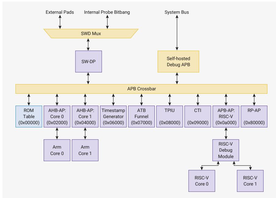
The numbers in brackets in Figure 10 are the addresses of the debug components within the debug address space. These correspond to values written to the SW-DP SELECT register for SWD accesses, or offsets from CORESIGHT_PERIPH_BASE for self-hosted debug access. All APs are accessible through the SW-DP, and all except the RP-AP are also accessible through self-hosted debug.
The SW-DP and RP-AP are in the always-on power domain, and are available once external power is applied and the power-on reset (POR) time has elapsed. All other APs in Figure 10 are available only once:
- 1. the power manager (POWMAN) has sequenced the first power up of the switched core domain
- 2. the OTP PSM has read critical hardware configuration flags from OTP
- 3. the system clock (
clk_sys) is running
3.5.1. Connecting to the SW-DP
The SW-DP defaults to the Dormant state at power-up or assertion of the external reset (RUN) pin. A Dormant-to-SWD sequence must be issued before beginning SWD operations. See the Arm Debug Interface specification, version 6, for details of Dormant/SWD state switching: https://developer.arm.com/documentation/ih0074/latest/
After a power-on, the following sequence can be used to connect to the SW-DP:
- 1. At least \( 8 \times \) SWCLK cycles with SWDIO high.
- 2. The 128-bit Selection Alert sequence:
0x19bc0ea2,0xe3ddafe9,0x86852d95,0x6209f392, LSB-first. - 3. Four SWCLK cycles with SWDIO low.
- 4. SWD activation code sequence :
0x1a, LSB first. - 5. At least 50 × SWCLK cycles with SWDIO high (line reset).
- 6. A DPIDR read to exit the Reset state
In order to wake up the system from a low power (P1.x) state, set the CDBGPWRUPREQ in the DP CTRL/STAT register, then poll CDBGPWRUPACK in the same register until set. In low-power states, only the SW-DP and RP-AP are accessible, as the remaining debug logic is unpowered.
3.5.2. Arm debug
There are two AHB5 Mem-APs, at offsets
0x02000
and
0x04000
in the debug address space, which are used to debug the two Arm Cortex-M33 processors. Each Mem-AP is an AHB5 manager which accesses a 32-bit downstream address space. This is the same address space accessed by a processor's load/store instructions, which includes system-level hardware such as memory and peripherals, and processor-internal hardware on the processor's private peripheral bus (PPB). Certain PPB registers are visible only when accessed from the Mem-AP, not when accessed by software running on the processor.
The AHB5 Mem-AP's own register map is defined in Arm's ADIV6 specification. Generally this is only of interest to those implementing their own debug translator, and the Mem-AP can be thought of simply as a bridge between a DP (such as RP2350's SW-DP) and a downstream address space.
The standard Arm debug registers used to debug software running on the Cortex-M33 can be found documented in the Arm v8-M Architecture Reference Manual , or the Cortex-M33 Technical Reference Manual, available from Arm Ltd. This datasheet also documents the core's internal registers in Section 3.7.5 .
The Mem-APs can access system peripherals and memory at exactly the same addresses they would be accessed by software running on the processor. However, the privilege and security of Mem-AP accesses may be different from the security state of the software running on the processor at the point it halted: the privilege and security of Mem-AP accesses is configured explicitly via its control and status word (CSW) register. Care must be taken when debugging Non-secure software which accesses the SIO, for example, because by default the debugger may access the Secure alias of the SIO, not the Non-secure alias which software will have been accessing.
The bus filters configured by the ACCESSCTRL bus access permission registers ( Section 10.6.2 ) treat bus accesses originating from the Mem-APs as distinct from bus accesses originating from software running on the processor. This means it is possible to lock software out from a peripheral, whilst still allowing debugger access.
3.5.3. RISC-V debug
There is a single APB Mem-AP, at offset
0x0a000
in the debug address space, which provides access only to the RISC-V Debug Module (DM). The DM is a standard component which the debugger uses to enumerate RISC-V harts present in the system, debug software running on each hart, and access the system bus. It is defined in the RISC-V debug specification, of which RP2350 implements version 0.13.2.
From the point of view of the RISC-V debug specification, the SW-DP and APB Mem-AP function jointly as the Debug Transport Module for this system. The DM is located at offset
0x0
in the APB-AP's downstream address space, and the registers are word-sized and byte-addressed, meaning the DM register addresses in the debug specification must be multiplied by 4 to get the correct APB address.
On RP2350, each core possesses exactly one hardware thread (hart). Core 0 has a hart ID of 0, and core 1 has a hart ID of 1. These hart IDs match the hart index used in the DM. This DM is also equipped with the hart array mask select extension, which allows multiple cores to be reset/halted/resumed simultaneously.
The DM is equipped with the System Bus Access (SBA) extension, which allows the debugger to access the system bus without halting either core. This can be used for minimally intrusive debug techniques like Segger RTT. SBA accesses
arbitrate with core 1's load/store port to access the system bus, but they are treated as distinct from core 1's accesses for the purpose of bus filtering (Section 10.6.2), which means it is possible to lock software out of a peripheral whilst retaining debug access. Processor load/stores in Debug mode are also treated as debug accesses for the purpose of bus filtering.
The DM is able to reset each core individually using the
dmcontrol.hartreset
control. This resets
only
the selected processor. The
dmcontrol.ndmreset
resets both processors
only
, which is the minimum requirement in the RISC-V debug specification. A full system reset, which includes the DM, can be performed using the
SYSRESETREQ
control in the SW-DP, a switched core domain reset configured in POWMAN and initiated by the watchdog, or any full-system reset such as the RUN pin. A PSM reset initiated by the watchdog can reset almost all system-level hardware except for the DM, but note that the DM becomes momentarily inaccessible whilst the system clock's clock generator is reset, which is the reason for
dmcontrol.ndmreset
resetting the processors only.
For details on the processor side of RISC-V debug, see Section 3.8.5. See also the Hazard3 source code at
github.com/Wren6991/Hazard3
, which includes the DM implementation under the
hdl/debug/dm/
directory.
3.5.4. Debug power domains
The SW-DP and the RP-AP are in the always-on power domain. This means they are available even when the system is in its lowest-power state, with the switched core domain (which includes the processors) fully powered down.
The remainder of the debug hardware is in the switched core domain. This is the same domain as the processors and system peripherals.
Setting the
CDBGPWRUPREQ
bit in the SW-DP's CTRL/STAT register will force a power up of the switched core domain, making the remaining debug hardware available. This power up takes some time, as it is sequenced by the 32 kHz low-power oscillator (Section 8.4), so the
CDBGPWRUPACK
bit must be polled to wait for the system to power up before attempting to access any APs other than the RP-AP. See Arm's ADIV6 specification for the SW-DP's register listing.
Note that the RP-AP is accessible without asserting
CDBGPWRUPREQ
, as it is always powered.
3.5.5. Software control of SWD pins
The
DBGFORCE
register in SYSCFG can be used to detach the SW-DP from the external debug pads, and instead bitbang the internal SWD signals directly from software. This is intended for a debug probe running on one core being used to debug the other core. For other use cases it is generally cleaner to use the self-hosted debug access to interface with the APs directly from the system bus.
3.5.6. Self-hosted debug
All APs shown in Figure 10, except for the RP-AP, have direct memory-mapped access from the system bus. This is known as self-hosted debug, because with care it allows running a debug host (i.e. a debugger) directly on-system. It can also be used to access the trace hardware, which can be used for self-hosted trace using the trace DMA FIFO. By default only Secure access is permitted, as the processor debug presents an opportunity for Non-secure code to interfere with the Secure context and/or perform Secure bus accesses.
The self-hosted debug window starts at address
0x40140000
(
CORESIGHT_PERIPH_BASE
). The offsets of the APs within this window are the same as the APs' addresses when accessed from the SW-DP.
Because of the blocking nature of the AHB-AP's DRW register, and its interactions with the Cortex-M33's arbitration of AHB-AP accesses with load/stores, certain accesses have potential to cause bus lockup due to circular bus stall dependencies. In particular, cores may not access their own AHB-APs through the self-hosted debug window, and AHB-APs may not access AHB-APs through the self-hosted debug window — attempting to do so will immediately return a bus fault. To reduce the opportunities for deadlock, a full APB crossbar is used to connect the SW-DP and the self-hosted debug port to the APs, so that for example self-hosted use of the Arm trace hardware will not interfere with an external debugger attaching via the AHB-APs.
There are some cases where a bus deadlock can not be avoided, such as a core using the other core's AHB-AP, via the self-hosted debug window, to access some other APB peripheral:
- 1. The access upstream of the APB's DRW register will not complete until the downstream access completes
- 2. The downstream access will not complete until it is granted access to the system APB bridge
- 3. Access to the APB bridge will not be granted until the upstream access, which is occupying the system APB bridge, completes
- 4. See point 1.
This situation can arise when running a self-hosted debugger on one core, and debugging code on the other core which accesses APB addresses. The deadlock is eventually broken when the APB bridge's 65536-cycle timeout expires, abandoning the transfer and returning a bus error to the origin of the upstream access. To avoid this, software should detect when it is about to use an AP to access an APB address (an address starting with
0x4
), and perform the access directly instead of using the Mem-AP.
This type of deadlock does not occur when the debugger accesses the bus with RISC-V System Bus Access, because the bus transfer upstream of the DM does not block on completion of the downstream access.
3.5.7. Trace
3.5.7.1. Overview
The ATB trace subsystem is based on the Coresight SoC-600M architecture, as shown in Figure 11 .
Figure 11. Trace Subsystem
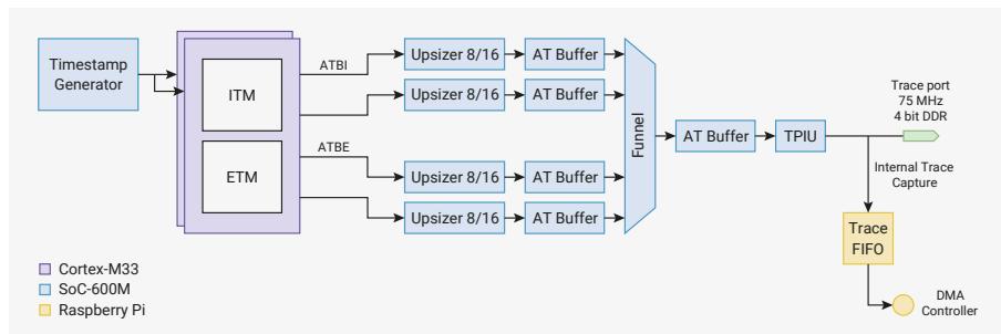
The trace subsystem captures trace messages from each of the Cortex-M33 ITM/ETM components, merges them into a single trace bus, and sends off-chip through the 4-bit DDR trace port for subsequent capture and analysis by a trace port analyser.
This allows the developer to review a detailed log of software executed on the processors. The advantage over conventional hardware debug is that it does this without halting the processors or affecting their execution timing, so you can diagnose software issues that are hard to reproduce under a debugger.
The trace subsystem comprises the following main components:
- • Timestamp Generator: Timestamps propagate to both Cortex-M33 processors, and are applied to ETM and ITM output so that the relative timing of their trace streams can be recovered.
- • Cortex-M33 ETM: Embedded Trace Macrocell, for real-time instruction flow messages generated from observations of the Cortex-M33's execution.
- • Cortex-M33 ITM: Instruction Trace Macrocell, for software-generated messages.
- • ATB Funnel: Merges the Cortex-M33 trace sources into a single trace stream using the timestamps from the Timestamp Generator.
- • TPIU: Trace Port Interface Unit, outputs trace data over trace port pins. The source-synchronous trace interface is 4-bits DDR, up to 75 MHz clock, giving a maximum trace data rate of up to 600 Mb/s.
- • Trace FIFO: Optionally captures the 32-bit TPIU trace stream on-device, from which point the DMA can transfer to main system SRAM.
See the Arm CoreSight ETM-M33 Technical Reference Manual for information about the Cortex-M33 ETM. See the SoC-600M Technical Reference Manual for information about the other trace components in Figure 11
The trace output clock is fixed at one half of
clk_sys
. At the maximum system frequency of 150 MHz this yields a 75 MHz TPIU output clock. The trace throughput is reduced at lower system clock frequencies, though this is rarely an issue in practice as the processor instruction throughput (and therefore the demand for trace output bandwidth) scales accordingly.
3.5.7.2. Trace FIFO
Trace output goes to one of two data sinks:
- • The four-bit TPIU interface streams data out of the chip through GPIOs, for capture by an external probe
- • The trace FIFO streams data into SRAM via the system DMA
The bandwidth of the DMA is greater than the bandwidth of the TPIU interface. Capturing into an on-chip buffer also allows trace to operate through a comparatively low-speed SWD probe without restricting trace bandwidth.
The operation is similar to a micro-trace buffer (MTB). However, all of system SRAM is available for trace. You can also use other DMA endpoints like the PIO and HSTX to implement your own trace data sinks, for example if you would prefer a wider and lower-frequency bus than the TPIU provides.
You must enable DMA access to the trace FIFO registers by setting the
DMA
bit in the
ACCESSCTRL
CORESIGHT_TRACE
register before attempting to DMA from this FIFO. Configure the DMA for DREQ
53
to select the trace FIFO.
3.5.7.3. List of trace FIFO registers
The trace FIFO registers start at a base address of
0x50700000
(defined as
CORESIGHT_TRACE_BASE
in the SDK).
Table 96. List of CORESIGHT_TRACE registers
| Offset | Name | Info |
|---|---|---|
| 0x0 | CTRL_STATUS | Control and status register |
| 0x4 | TRACE_CAPTURE_FIFO | FIFO for trace data captured from the TPIU |
CORESIGHT_TRACE: CTRL_STATUS Register
Offset: 0x0
Description
Control and status register
Table 97. CTRL_STATUS Register
| Bits | Description | Type | Reset |
|---|---|---|---|
| 31:2 | Reserved. | - | - |
| 1 | TRACE_CAPTURE_FIFO_OVERFLOW : This status flag is set high when trace data has been dropped due to the FIFO being full at the point trace data was sampled. Write 1 to acknowledge and clear the bit. | RW | 0x0 |
| Bits | Description | Type | Reset |
|---|---|---|---|
| 0 | TRACE_CAPTURE_FIFO_FLUSH: Set to 1 to continuously hold the trace FIFO in a flushed state and prevent overflow. Before clearing this flag, configure and start a DMA channel with the correct DREQ for the TRACE_CAPTURE_FIFO register. Clear this flag to begin sampling trace data, and set once again once the trace capture buffer is full. You must configure the TPIU in order to generate trace packets to be captured, as well as components like the ETM further upstream to generate the event stream propagated to the TPIU. | RW | 0x1 |
CORESIGHT_TRACE: TRACE_CAPTURE_FIFO Register
Offset: 0x4
Description
FIFO for trace data captured from the TPIU
Table 98.
TRACE_CAPTURE_FIFO
Register
| Bits | Description | Type | Reset |
|---|---|---|---|
| 31:0 | RDATA: Read from an 8 x 32-bit FIFO containing trace data captured from the TPIU. Hardware pushes to the FIFO on rising edges of clk_sys, when either of the following is true:
These conditions are in accordance with Arm Coresight Architecture Spec v3.0 section D3.3.3: Decoding requirements for Trace Capture Devices The data captured into the FIFO is the full 32-bit TRACEDATA bus output by the TPIU. Note that the TPIU is a DDR output at half of clk_sys, therefore this interface can capture the full 32-bit TPIU DDR output bandwidth as it samples once per active edge of the TPIU output clock. | RF | 0x00000000 |
3.5.8. Rescue reset
A rescue reset is a full system reset, similar to asserting the RUN pin low, which also sets a flag telling the bootrom to halt before running any user software. This is performed over the SWD bus using the RP-AP, and can be performed even when system clocks are stopped and the switched core power domain is powered down. This is used in the case where the chip has locked up, for example if code has been programmed into flash which permanently halts the system clock: since the debugger can no longer communicate with the processors to return the system to a working state, more drastic action is needed. This functionality was provided by the Rescue DP on RP2040, but on RP2350 it is provided by the RP-AP, to avoid mandatory use of multidrop SWD.
A rescue is invoked by setting and then clearing the CTRL.RESCUE_RESTART bit in the RP-AP. This causes a hard reset of the chip, and sets CHIP_RESET.RESCUE_FLAG to indicate that a rescue reset took place. The bootrom checks this flag almost immediately in the initial boot process (before watchdog, flash or USB boot), acknowledges by clearing the bit, then halts the processor. This leaves the system in a safe state, with the system clock running, so that the debugger can reattach to the cores and load fresh code.
3.5.9. Security
By default, the SWD debug access port allows an external debugger to access all system memory and peripherals, and to observe and change the execution of software running on the processors. If boot signature enforcement is enabled (Section 10.1.1), debug access becomes a security concern, as it is able to sidestep this protection. To account for this, RP2350 supports progressively locking down the debug port using configuration in on-chip OTP storage.
Conceptually there are two control bits: debug disable, and secure debug disable. Debug disable is intended to completely cut off debug access to the processors and the system bus, whilst the secure debug disable forbids Secure bus accesses, and halting of processors in the Secure state, but still allows Non-secure software to be debugged as normal. There are two ways to set these control bits:
- • Setting the relevant OTP critical flag:
CRIT1.DEBUG_DISABLEorCRIT1.SECURE_DEBUG_DISABLEto set the debug disable or secure debug disable, respectively - • Installing a 128-bit fixed debug key as OTP key 5 or 6 (Section 3.5.9.2)
OTP configuration changes take effect at the next reset of the OTP block.
Once debug has been disabled, software can re-enable debug using the OTP
DEBUGEN
register, which allows the secure and overall debug enable to be cleared individually for each processor. For example, Secure software may implement a shell where users can authenticate using a cryptographic challenge to enable debug on systems where it is disabled by default. The
DEBUGEN
register belongs to the processor cold reset domain, so it is preserved over a PSM reset starting from as early as OTP (the second PSM stage). This allows almost a full system reset without losing debug access.
To avoid accidental writes of the
DEBUGEN
register, its bits can be individually locked using the matching bits in
DEBUGEN_LOCK
.
This offers increasing levels of debug protection:
- 1. Fully open: no keys installed and no OTP debug disable flags are set. This is the most convenient configuration for product development.
- 2. Access with key only: at least one key is installed, but no OTP debug disable flags are set.
- 3. No access even with key (an OTP debug disable flag is set), but Secure code can enable debug access by writing to
DEBUGEN. - 4. No access even with key (an OTP debug disable flag is set), and
DEBUGENis locked byDEBUGEN_LOCK.
3.5.9.1. Effects of debug disables
The secure debug disable flag (
CRIT1.SECURE_DEBUG_DISABLE
) has the following effects:
- • Set Secure AP enable signals for Arm core 0 and core 1 AHB-APs to 0.
- ◦ This prevents the APs from performing Secure bus accesses (including to the PPB).
- ◦ Status is reported in the
SDeviceEnflag of the AHB-APCSWregister.
- • Set the Cortex-M33
SPIDENandSPNIDENsignals for both cores to 0.- ◦ This prevents the cores from being halted or traced whilst in the Secure state.
- • Disable the factory test JTAG interface (Section 10.10).
Both AHB-APs'
CSW.HNONSEC
bits default to 0, generating Secure bus accesses. If the secure debug disable flag is set, these bits must be set to 1 to generate Non-Secure bus accesses.
The debug disable flag (
CRIT1.DEBUG_DISABLE
) has all of the effects of the secure debug disable flag. It also has the following additional effects:
- • Set AP enable signals for Arm core 0 and core 1 AHB-APs to 0.
- ◦ This prevents the APs from performing any bus accesses at all (including to the PPB).
- ◦ Status is reported in the
DeviceEnflag of the AHB-APCSWregister.
- • Set AP enable signal for RISC-V DM APB-AP to 0.
- ◦ This prevents the AP from accessing the RISC-V Debug Module.
- ◦ Status is reported in the
DeviceEnflag of the APB-APCSWregister.
- • Set
DBGENandNIDENsignals for the CTI to 0.
On RISC-V
CRIT1.SECURE_DEBUG_DISABLE
has no useful effect. Debug-mode accesses from the cores always have Secure and Privileged bus attributes, except when reduced by
FORCE_CORE_NS
. Likewise, System Bus Access via the Debug Module is always Secure and Privileged, unless
FORCE_CORE_NS.CORE1
is set, in which case it is Non-secure and Privileged. Use the
CRIT1.DEBUG_DISABLE
flag on RISC-V.
3.5.9.2. Debug keys
Section 13.5.2 describes the OTP hardware access keys. Hardware reads OTP access keys into hidden registers as part of the OTP power-up sequence which takes place after an OTP reset, and the corresponding OTP locations then become inaccessible. OTP keys 5 and 6 are special in that they control access to the SWD debug hardware in addition to functioning as normal OTP page keys.
A debug key is a 128-bit fixed challenge. Installing a debug key in OTP locks down debug access, and it remains locked until the debug host writes a matching key value through the RP-AP
DBGKEY
register. This is a write-only interface.
To install a debug key, first program the OTP locations starting from
KEY5_0
or
KEY6_0
. These locations are ECC-protected. Once you have programmed the 128-bit key value and read it back to confirm the correct value is programmed, write the raw bit pattern
0x010101
to
KEY5_VALID
or
KEY6_VALID
to mark the key as valid. The validity takes effect at the next reset of the OTP block.
Once a key is valid, the OTP storage locations for that key become inaccessible for both reads and writes. Only the OTP power-up state machine (Section 13.3.4) can read the key.
The effect of installing debug keys depends on which of key 5 and 6 are installed:
- • If key 5 or key 6 is valid, and no matching key (either) has been entered through the RP-AP, all debug is disabled. This has the same effect as setting
CRIT1.DEBUG_DISABLE. - • If key 5 is valid, and no matching key (key 5 specifically) has been entered through the RP-AP, Secure debug is disabled. This has the same effect as writing
CRIT1.SECURE_DEBUG_DISABLE.
When both keys are installed, key 5 provides both Secure and Non-secure debug access, and key 6 provides Non-secure debug access only. When only a single key is installed, that key provides both Secure and Non-secure debug access.
To enter a key over SWD, first write a 1 to
DBGKEY.RESET
. Then sequentially write 128 bits to
DBGKEY.DATA
, each accompanied by a 1 written to
DBGKEY.PUSH
. Write the data LSB-first, starting with the lowest-numbered OTP row.
Assuming you wrote a value that matched one of the installed debug keys, debug unlocks after the 128th push. The
SDeviceEn
and
DeviceEn
flags in the Mem-AP
CSW
registers indicate success or failure.
Failure to supply a matching key through the RP-AP disables debug if it would otherwise be enabled. However, supplying a key does not enable if it is already disabled for other reasons. For example, if
CRIT1.DEBUG_DISABLE
is set, and
DEBUGEN is clear, debug is be disabled no matter the state of the debug keys and the RP-AP.
3.5.10. RP-AP
The RP-AP is a small register block which is always accessible over SWD. RP-AP access does not require the switched core domain to be powered up, or any internal system clock generators to be running.
3.5.10.1. List of registers
The RP-AP registers start at offset 0x80000 in the debug address space, which is accessed via address 0x80000 in the SW-DP's SELECT register. Unlike the other APs, it can not be accessed directly from the system bus.
Table 99. List of RP-AP registers
| Offset | Name | Info |
|---|---|---|
| 0x000 | CTRL | This register is primarily used for DFT but can also be used to overcome some power up problems. However, it should not be used to force power up of domains. Use DBG_POW_OVRD for that. |
| 0x004 | DBGKEY | Serial key load interface (write-only) |
| 0x008 | DBG_POW_STATE_SWCORE | This register indicates the state of the power sequencer for the switched-core domain. The sequencer timing is managed by the POWMAN_SEQ_* registers. See the header file for those registers for more information on the timing. Power up of the domain commences by clearing bit 0 ( IS_PD ) then bits 1-8 are set in sequence. Bit 8 ( IS_PU ) indicates the sequence is complete. Power down of the domain commences by clearing bit 8 ( IS_PU ) then bits 7-1 are cleared in sequence. Bit 0 ( IS_PU ) is then set to indicate the sequence is complete. Bits 9-11 describe the states of the power manager clocks which change as clock generators in the switched-core become available following switched-core power up. This bus can be sent to GPIO for debug. See DBG_POW_OUTPUT_TO_GPIO in the DBG_POW_OVRD register. |
| 0x00c | DBG_POW_STATE_XIP | This register indicates the state of the power sequencer for the XIP domain. The sequencer timing is managed by the POWMAN_SEQ_* registers. See the header file for those registers for more information on the timing. Power up of the domain commences by clearing bit 0 ( IS_PD ) then bits 1-8 are set in sequence. Bit 8 ( IS_PU ) indicates the sequence is complete. Power down of the domain commences by clearing bit 8 ( IS_PU ) then bits 7-1 are cleared in sequence. Bit 0 ( IS_PU ) is then set to indicate the sequence is complete. |
| Offset | Name | Info |
|---|---|---|
| 0x010 | DBG_POW_STATE_SRAM0 | This register indicates the state of the power sequencer for the SRAM0 domain. The sequencer timing is managed by the POWMAN_SEQ_* registers. See the header file for those registers for more information on the timing. Power up of the domain commences by clearing bit 0 (IS_PD) then bits 1-8 are set in sequence. Bit 8 (IS_PU) indicates the sequence is complete. Power down of the domain commences by clearing bit 8 (IS_PU) then bits 7-1 are cleared in sequence. Bit 0 (IS_PU) is then set to indicate the sequence is complete. |
| 0x014 | DBG_POW_STATE_SRAM1 | This register indicates the state of the power sequencer for the SRAM1 domain. The sequencer timing is managed by the POWMAN_SEQ_* registers. See the header file for those registers for more information on the timing. Power up of the domain commences by clearing bit 0 (IS_PD) then bits 1-8 are set in sequence. Bit 8 (IS_PU) indicates the sequence is complete. Power down of the domain commences by clearing bit 8 (IS_PU) then bits 7-1 are cleared in sequence. Bit 0 (IS_PU) is then set to indicate the sequence is complete. |
| 0x018 | DBG_POW_OVRD | This register allows external control of the power sequencer outputs for all the switched power domains. If any of the power sequencers stall at any stage then force power up operation of all domains by running this sequence:
|
| 0x01c | DBG_POW_OUTPUT_TO_GPIO | Send some, or all, bits of DBG_POW_STATE_SWCORE to gpios. Bit 0 sends bit 0 of DBG_POW_STATE_SWCORE to GPIO 34 Bit 1 sends bit 1 of DBG_POW_STATE_SWCORE to GPIO 35 Bit 2 sends bit 2 of DBG_POW_STATE_SWCORE to GPIO 36 . . Bit 11 sends bit 11 of DBG_POW_STATE_SWCORE to GPIO 45 |
| 0xdfc | IDR | Standard Coresight ID Register |
RP_AP: CTRL Register
Offset: 0x000
Description
This register is primarily used for DFT but can also be used to overcome some power up problems. However, it should not be used to force power up of domains. Use DBG_POW_OVRD for that.
Table 100. CTRL Register
| Bits | Description | Type | Reset |
|---|---|---|---|
| 31 | RESCUE_RESTART : Allows debug of boot problems by restarting the chip with minimal boot code execution. Write to 1 to put the chip in reset then write to 0 to restart the chip with the rescue flag set. The rescue flag is in the POWMAN_CHIP_RESET register and is read by boot code. The rescue flag is cleared by writing 0 to POWMAN_CHIP_RESET_RESCUE_FLAG or by resetting the chip by any means other than RESCUE_RESTART. | RW | 0x0 |
| 30 | SPARE : Unused | RW | 0x0 |
| 29:7 | Reserved. | - | - |
| 6 | DBG_FRCE_GPIO_LPCK : Allows chip start-up when the Low Power Oscillator (LPOSC) is inoperative or malfunctioning and also allows the initial power sequencing rate to be adjusted. Write to 1 to force the LPOSC output to be driven from a GPIO (gpio20 on 80-pin package, gpio34 on the 60-pin package). If the LPOSC is inoperative or malfunctioning it may also be necessary to set the LPOSC_STABLE_FRCE bit in this register. The user must provide a clock on the GPIO. For normal operation use a clock running at around 32kHz. Adjusting the frequency will speed up or slow down the initial power-up sequence. | RW | 0x0 |
| 5 | LPOSC_STABLE_FRCE : Allows the chip to start-up even though the Low Power Oscillator (LPOSC) is failing to set its stable flag. Initial power sequencing is clocked by LPOSC at around 32kHz but does not start until the LPOSC declares itself to be stable. If the LPOSC is otherwise working correctly the chip will boot when this bit is set. If the LPOSC is not working then DBG_FRCE_GPIO_LPCK must be set and an external clock provided. | RW | 0x0 |
| 4 | POWMAN_DFT_ISO_OFF : Holds the isolation gates between power domains in the open state. This is intended to hold the gates open for DFT and power manager debug. It is not intended to force the isolation gates open. Use the overrides in DBG_POW_OVRD to force the isolation gates open or closed. | RW | 0x0 |
| 3 | POWMAN_DFT_PWRON : Holds the power switches on for all domains. This is intended to keep the power on for DFT and debug, rather than for switching the power on. The power switches are not sequenced and the sudden demand for current could cause the always-on power domain to brown out. This register is in the always-on domain therefore chaos could ensue. It is recommended to use the DBG_POW_OVRD controls instead. | RW | 0x0 |
| 2 | POWMAN_DBGMODE : This prevents the power manager from powering down and resetting the switched-core power domain. It is intended for DFT and for debugging the power manager after the chip has booted. It cannot be used to force initial power on because it simultaneously deasserts the reset. | RW | 0x0 |
| 1 | JTAG_FUNCSEL : Multiplexes the JTAG ports onto GPIO0-3 | RW | 0x0 |
| 0 | JTAG_TRSTN : Resets the JTAG module. Active low. | RW | 0x0 |
RP_AP: DBGKEY Register
Offset: 0x004
Description
Serial key load interface (write-only)
Table 101. DBGKEY Register
| Bits | Description | Type | Reset |
|---|---|---|---|
| 31:3 | Reserved. | - | - |
| Bits | Description | Type | Reset |
|---|---|---|---|
| 2 | RESET : Reset (before sending a new key) | RW | 0x0 |
| 1 | PUSH | RW | 0x0 |
| 0 | DATA | RW | 0x0 |
RP_AP: DBG_POW_STATE_SWCORE Register
Offset: 0x008
Description
This register indicates the state of the power sequencer for the switched-core domain.
The sequencer timing is managed by the POWMAN_SEQ_* registers. See the header file for those registers for more information on the timing.
Power up of the domain commences by clearing bit 0 (IS_PD) then bits 1-8 are set in sequence. Bit 8 (IS_PU) indicates the sequence is complete.
Power down of the domain commences by clearing bit 8 (IS_PU) then bits 7-1 are cleared in sequence. Bit 0 (IS_PU) is then set to indicate the sequence is complete.
Bits 9-11 describe the states of the power manager clocks which change as clock generators in the switched-core become available following switched-core power up.
This bus can be sent to GPIO for debug. See DBG_POW_OUTPUT_TO_GPIO in the DBG_POW_OVRD register.
Table 102.
DBG_POW_STATE_SW
CORE Register
| Bits | Description | Type | Reset |
|---|---|---|---|
| 31:12 | Reserved. | - | - |
| 11 | USING_FAST_POWCK : Indicates the source of the power manager clock. On switched-core power up the clock switches from the LPOSC to clk_ref and this flag will be set. clk_ref will be running from the ROSC initially but will switch to XOSC when it comes available. On switched-core power down the clock switches to LPOSC and this flag will be cleared. | RO | 0x0 |
| 10 | WAITING_POWCK
: Indicates the switched-core power sequencer is waiting for the power manager clock to update. On switched-core power up the clock switches from the LPOSC to clk_ref. clk_ref will be running from the ROSC initially but will switch to XOSC when it comes available. On switched-core power down the clock switches to LPOSC. If the switched-core power up sequence stalls with this flag active then it means clk_ref is not running which indicates a problem with the ROSC. If that happens then set DBG_POW_RESTART_FROM_XOSC in the DBG_POW_OVRD register to avoid using the ROSC. If the switched-core power down sequence stalls with this flag active then it means LPOSC is not running. The solution is to not stop LPOSC when the switched-core power domain is powered. | RO | 0x0 |
| 9 | WAITING_TIMCK : Indicates that the switched-core power sequencer is waiting for the AON-Timer to update. On switched-core power-up there is nothing to be done. The AON-Timer continues to run from the LPOSC so this flag will not be set. Software decides whether to switch the AON-Timer clock to XOSC (via clk_ref). On switched-core power-down the sequencer will switch the AON-Timer back to LPOSC if software switched it to XOSC. During the switchover the WAITING_TIMCK flag will be set. If the switched-core power down sequence stalls with this flag active then the only recourse is to reset the chip and change software to not select XOSC as the AON-Timer source. | RO | 0x0 |
| 8 | IS_PU : Indicates the power somain is fully powered up. | RO | 0x0 |
| 7 | RESET_FROM_SEQ : Indicates the state of the reset to the power domain. | RO | 0x0 |
| Bits | Description | Type | Reset |
|---|---|---|---|
| 6 | ENAB_ACK : Indicates the state of the enable to the power domain. | RO | 0x0 |
| 5 | ISOLATE_FROM_SEQ : Indicates the state of the isolation control to the power domain. | RO | 0x0 |
| 4 | LARGE_ACK : Indicates the state of the large power switches for the power domain. | RO | 0x0 |
| 3 | SMALL_ACK2
: The small switches are split into 3 chains. In the power up sequence they are switched on separately to allow management of the VDD rise time. In the power down sequence they switch off simultaneously with the large power switches. This bit indicates the state of the last element in small power switch chain 2. | RO | 0x0 |
| 2 | SMALL_ACK1 : This bit indicates the state of the last element in small power switch chain 1. | RO | 0x0 |
| 1 | SMALL_ACK0 : This bit indicates the state of the last element in small power switch chain 0. | RO | 0x0 |
| 0 | IS_PD : Indicates the power somain is fully powered down. | RO | 0x0 |
RP_AP: DBG_POW_STATE_XIP Register
Offset: 0x00c
Description
This register indicates the state of the power sequencer for the XIP domain.
The sequencer timing is managed by the POWMAN_SEQ_* registers. See the header file for those registers for more information on the timing.
Power up of the domain commences by clearing bit 0 (IS_PD) then bits 1-8 are set in sequence. Bit 8 (IS_PU) indicates the sequence is complete.
Power down of the domain commences by clearing bit 8 (IS_PU) then bits 7-1 are cleared in sequence. Bit 0 (IS_PU) is then set to indicate the sequence is complete.
Table 103.
DBG_POW_STATE_XIP
Register
| Bits | Description | Type | Reset |
|---|---|---|---|
| 31:9 | Reserved. | - | - |
| 8 | IS_PU : Indicates the power somain is fully powered up. | RO | 0x0 |
| 7 | RESET_FROM_SEQ : Indicates the state of the reset to the power domain. | RO | 0x0 |
| 6 | ENAB_ACK : Indicates the state of the enable to the power domain. | RO | 0x0 |
| 5 | ISOLATE_FROM_SEQ : Indicates the state of the isolation control to the power domain. | RO | 0x0 |
| 4 | LARGE_ACK : Indicates the state of the large power switches for the power domain. | RO | 0x0 |
| 3 | SMALL_ACK2
: The small switches are split into 3 chains. In the power up sequence they are switched on separately to allow management of the VDD rise time. In the power down sequence they switch off simultaneously with the large power switches. This bit indicates the state of the last element in small power switch chain 2. | RO | 0x0 |
| 2 | SMALL_ACK1 : This bit indicates the state of the last element in small power switch chain 1. | RO | 0x0 |
| 1 | SMALL_ACK0 : This bit indicates the state of the last element in small power switch chain 0. | RO | 0x0 |
| Bits | Description | Type | Reset |
|---|---|---|---|
| 0 | IS_PD : Indicates the power somain is fully powered down. | RO | 0x0 |
RP_AP: DBG_POW_STATE_SRAM0 Register
Offset: 0x010
Description
This register indicates the state of the power sequencer for the SRAM0 domain.
The sequencer timing is managed by the POWMAN_SEQ_* registers. See the header file for those registers for more information on the timing.
Power up of the domain commences by clearing bit 0 (IS_PD) then bits 1-8 are set in sequence. Bit 8 (IS_PU) indicates the sequence is complete.
Power down of the domain commences by clearing bit 8 (IS_PU) then bits 7-1 are cleared in sequence. Bit 0 (IS_PU) is then set to indicate the sequence is complete.
Table 104.
DBG_POW_STATE_SR
AM0 Register
| Bits | Description | Type | Reset |
|---|---|---|---|
| 31:9 | Reserved. | - | - |
| 8 | IS_PU : Indicates the power somain is fully powered up. | RO | 0x0 |
| 7 | RESET_FROM_SEQ : Indicates the state of the reset to the power domain. | RO | 0x0 |
| 6 | ENAB_ACK : Indicates the state of the enable to the power domain. | RO | 0x0 |
| 5 | ISOLATE_FROM_SEQ : Indicates the state of the isolation control to the power domain. | RO | 0x0 |
| 4 | LARGE_ACK : Indicates the state of the large power switches for the power domain. | RO | 0x0 |
| 3 | SMALL_ACK2
: The small switches are split into 3 chains. In the power up sequence they are switched on separately to allow management of the VDD rise time. In the power down sequence they switch off simultaneously with the large power switches. This bit indicates the state of the last element in small power switch chain 2. | RO | 0x0 |
| 2 | SMALL_ACK1 : This bit indicates the state of the last element in small power switch chain 1. | RO | 0x0 |
| 1 | SMALL_ACK0 : This bit indicates the state of the last element in small power switch chain 0. | RO | 0x0 |
| 0 | IS_PD : Indicates the power somain is fully powered down. | RO | 0x0 |
RP_AP: DBG_POW_STATE_SRAM1 Register
Offset: 0x014
Description
This register indicates the state of the power sequencer for the SRAM1 domain.
The sequencer timing is managed by the POWMAN_SEQ_* registers. See the header file for those registers for more information on the timing.
Power up of the domain commences by clearing bit 0 (IS_PD) then bits 1-8 are set in sequence. Bit 8 (IS_PU) indicates the sequence is complete.
Power down of the domain commences by clearing bit 8 (IS_PU) then bits 7-1 are cleared in sequence. Bit 0 (IS_PU) is then set to indicate the sequence is complete.
Table 105.
DBG_POW_STATE_SR
AM1 Register
| Bits | Description | Type | Reset |
|---|---|---|---|
| 31:9 | Reserved. | - | - |
| 8 | IS_PU : Indicates the power somain is fully powered up. | RO | 0x0 |
| 7 | RESET_FROM_SEQ : Indicates the state of the reset to the power domain. | RO | 0x0 |
| 6 | ENAB_ACK : Indicates the state of the enable to the power domain. | RO | 0x0 |
| 5 | ISOLATE_FROM_SEQ : Indicates the state of the isolation control to the power domain. | RO | 0x0 |
| 4 | LARGE_ACK : Indicates the state of the large power switches for the power domain. | RO | 0x0 |
| 3 | SMALL_ACK2
: The small switches are split into 3 chains. In the power up sequence they are switched on separately to allow management of the VDD rise time. In the power down sequence they switch off simultaneously with the large power switches. This bit indicates the state of the last element in small power switch chain 2. | RO | 0x0 |
| 2 | SMALL_ACK1 : This bit indicates the state of the last element in small power switch chain 1. | RO | 0x0 |
| 1 | SMALL_ACK0 : This bit indicates the state of the last element in small power switch chain 0. | RO | 0x0 |
| 0 | IS_PD : Indicates the power somain is fully powered down. | RO | 0x0 |
RP_AP: DBG_POW_OVRD Register
Offset: 0x018
Description
This register allows external control of the power sequencer outputs for all the switched power domains. If any of the power sequencers stall at any stage then force power up operation of all domains by running this sequence:
- • set DBG_POW_OVRD = 0x3b to force small power switches on, large power switches off, resets on and isolation on
- • allow time for the domain power supplies to reach full rail
- • set DBG_POW_OVRD = 0x3b to force large power switches on
- • set DBG_POW_OVRD = 0x37 to remove isolation
- • set DBG_POW_OVRD = 0x17 to remove resets
Table 106.
DBG_POW_OVRD
Register
| Bits | Description | Type | Reset |
|---|---|---|---|
| 31:7 | Reserved. | - | - |
| 6 | DBG_POW_RESTART_FROM_XOSC : By default the system begins boot as soon as a clock is available from the ROSC, then it switches to the XOSC when it is available. This is done because the XOSC takes several ms to start up. If there is a problem with the ROSC then the default behaviour can be changed to not use the ROSC and wait for XOSC. However, this requires a mask change to modify the reset value of the Power Manager START_FROM_XOSC register. To allow experimentation the default can be temporarily changed by setting this register bit to 1. After setting this bit the core must be reset by a Coresight dprst or a rescue reset (see RESCUE_RESTART in the RP_AP_CTRL register above). A power-on reset, brown-out reset or RUN pin reset will reset this control and revert to the default behaviour. | RW | 0x0 |
| Bits | Description | Type | Reset |
|---|---|---|---|
| 5 | DBG_POW_RESET : When DBG_POW_OVRD_RESET=1 this register bit controls the resets for all domains. 1 = reset. 0 = not reset. | RW | 0x0 |
| 4 | DBG_POW_OVRD_RESET : Enables DBG_POW_RESET to control the resets for the power manager and the switched-core. Essentially that is everything except the Coresight 2-wire interface and the RP_AP registers. | RW | 0x0 |
| 3 | DBG_POW_ISO : When DBG_POW_OVRD_ISO=1 this register bit controls the isolation gates for all domains. 1 = isolated. 0 = not isolated. | RW | 0x0 |
| 2 | DBG_POW_OVRD_ISO : Enables DBG_POW_ISO to control the isolation gates between domains. | RW | 0x0 |
| 1 | DBG_POW_OVRD_LARGE_REQ : Turn on the large power switches for all domains. This should not be done until sufficient time has been allowed for the small switches to bring the supplies up. Switching the large switches on too soon risks browning out the always-on domain and corrupting these very registers. | RW | 0x0 |
| 0 | DBG_POW_OVRD_SMALL_REQ : Turn on the small power switches for all domains. This switches on chain 0 for each domain and switches off chains 2 & 3 and the large power switch chain. This will bring the power up for all domains without browning out the always-on power domain. | RW | 0x0 |
RP_AP: DBG_POW_OUTPUT_TO_GPIO Register
Offset: 0x01c
Description
Send some, or all, bits of DBG_POW_STATE_SWCORE to gpios.
Bit 0 sends bit 0 of DBG_POW_STATE_SWCORE to GPIO 34
Bit 1 sends bit 1 of DBG_POW_STATE_SWCORE to GPIO 35
Bit 2 sends bit 2 of DBG_POW_STATE_SWCORE to GPIO 36
1. +
2. + Bit 11 sends bit 11 of DBG_POW_STATE_SWCORE to GPIO 45
Table 107.
DBG_POW_OUTPUT_TO_GPIO Register
| Bits | Description | Type | Reset |
|---|---|---|---|
| 31:12 | Reserved. | - | - |
| 11:0 | ENABLE | RW | 0x000 |
RP_AP: IDR Register
Offset: 0xdfc
Table 108. IDR Register
| Bits | Description | Type | Reset |
|---|---|---|---|
| 31:0 | Standard Coresight ID Register | RO | - |
3.6. Cortex-M33 coprocessors
The Cortex-M33 features a coprocessor port which transfers up to 64 bits per cycle between the processor and certain closely-coupled hardware. The Cortex-M33's built-in floating-point unit is an example of such a coprocessor, but RP2350 adds three device-specific coprocessors to this interface. The following sections document these coprocessors.
Before accessing a coprocessor from Secure code, that coprocessor must first be enabled by setting the corresponding bit in the CPACR. Before accessing from the Non-secure state, the corresponding bits in the NSACR and CPACR_NS registers must be set.
The RISC-V processors on RP2350 do not have access to the Cortex-M33 coprocessors.
3.6.1. GPIO coprocessor (GPIOC)
Coprocessor port 0 provides low-overhead access from the Cortex-M33 processors to the GPIO registers in the SIO (Section 3.1.3). This enables a single coprocessor instruction to sample all 48 GPIOs, or to set/clear/write any single GPIO, among other functionality.
Non-secure accesses are filtered according to the GPIO_NSMASK0 and GPIO_NSMASK1 registers in ACCESSCTRL. GPIOs not granted for Non-secure use will ignore writes from the Non-secure state, and read back as zero when read from the Non-secure state.
3.6.1.1. OUT mask write instructions
These instructions write to multiple bits in the SIO GPIO_OUT and GPIO_HI_OUT registers.
| Mnemonic | Armv8-M Instruction | Operation |
|---|---|---|
| gpioc_lo_out_put | mcr p0, #0, Rt, c0, c0 | sio_hw→gpio_out = Rt; |
| gpioc_lo_out_xor | mcr p0, #1, Rt, c0, c0 | sio_hw→gpio_togl = Rt; |
| gpioc_lo_out_set | mcr p0, #2, Rt, c0, c0 | sio_hw→gpio_set = Rt; |
| gpioc_lo_out_clr | mcr p0, #3, Rt, c0, c0 | sio_hw→gpio_clr = Rt; |
| gpioc_hi_out_put | mcr p0, #0, Rt, c0, c1 | sio_hw→gpio_hi_out = Rt; |
| gpioc_hi_out_xor | mcr p0, #1, Rt, c0, c1 | sio_hw→gpio_hi_togl = Rt; |
| gpioc_hi_out_set | mcr p0, #2, Rt, c0, c1 | sio_hw→gpio_hi_set = Rt; |
| gpioc_hi_out_clr | mcr p0, #3, Rt, c0, c1 | sio_hw→gpio_hi_clr = Rt; |
| gpioc_hilo_out_put | mcr p0, #0, Rt, Rt2, c0 | Simultaneously:
sio_hw→gpio_out = Rt; sio_hw→gpio_hi_out = Rt2; |
| gpioc_hilo_out_xor | mcr p0, #1, Rt, Rt2, c0 | Simultaneously:
sio_hw→gpio_togl = Rt; sio_hw→gpio_hi_togl = Rt2; |
| gpioc_hilo_out_set | mcr p0, #2, Rt, Rt2, c0 | Simultaneously:
sio_hw→gpio_set = Rt; sio_hw→gpio_hi_set = Rt2; |
| gpioc_hilo_out_clr | mcr p0, #3, Rt, Rt2, c0 | Simultaneously:
sio_hw→gpio_clr = Rt; sio_hw→gpio_hi_clr = Rt2; |
3.6.1.2. OE mask write instructions
These instructions write to multiple bits in the SIO GPIO_OE and GPIO_HI_OE registers.
| Mnemonic | Armv8-M Instruction | Operation |
|---|---|---|
| gpioc_lo_oe_put | mcr p0, #0, Rt, c0, c4 | sio_hw→gpio_oe = Rt; |
| gpioc_lo_oe_xor | mcr p0, #1, Rt, c0, c4 | sio_hw→gpio_oe_togl = Rt; |
| gpioc_lo_oe_set | mcr p0, #2, Rt, c0, c4 | sio_hw→gpio_oe_set = Rt; |
| gpioc_lo_oe_clr | mcr p0, #3, Rt, c0, c4 | sio_hw→gpio_oe_clr = Rt; |
| gpioc_hi_oe_put | mcr p0, #0, Rt, c0, c5 | sio_hw→gpio_hi_oe = Rt; |
| gpioc_hi_oe_xor | mcr p0, #1, Rt, c0, c5 | sio_hw→gpio_hi_oe_togl = Rt; |
| Mnemonic | Armv8-M Instruction | Operation |
|---|---|---|
| gpioc_hi_oe_set | mcr p0, #2, Rt, c0, c5 | sio_hw→gpioc_hi_oe_set = Rt; |
| gpioc_hi_oe_clr | mcr p0, #3, Rt, c0, c5 | sio_hw→gpioc_hi_oe_clr = Rt; |
| gpioc_hilo_oe_put | mccr p0, #0, Rt, Rt2, c4 | Simultaneously: sio_hw→gpioc_oe = Rt; sio_hw→gpioc_hi_oe = Rt2; |
| gpioc_hilo_oe_xor | mccr p0, #1, Rt, Rt2, c4 | Simultaneously: sio_hw→gpioc_oe_togl = Rt; sio_hw→gpioc_hi_oe_togl = Rt2; |
| gpioc_hilo_oe_set | mccr p0, #2, Rt, Rt2, c4 | Simultaneously: sio_hw→gpioc_oe_set = Rt; sio_hw→gpioc_hi_oe_set = Rt2; |
| gpioc_hilo_oe_clr | mccr p0, #3, Rt, Rt2, c4 | Simultaneously: sio_hw→gpioc_oe_clr = Rt; sio_hw→gpioc_hi_oe_clr = Rt2; |
3.6.1.3. Single-bit write instructions
These instructions write to a single, indexed bit in either the GPIO_OUT and GPIO_HI_OUT registers, or the GPIO_OE and GPIO_HI_OE registers.
| Mnemonic | Armv8-M Instruction | Operation |
|---|---|---|
| gpioc_bit_out_put | mccr p0, #4, Rt, Rt2, c0 | Write a 1-bit value to any output. Equivalent to: if (Rt2 & 1) gpioc_hilo_out_set(1ull << Rt); else gpioc_hilo_out_clr(1ull << Rt); |
| gpioc_bit_out_xor | mcr p0, #5, Rt, c0, c0 | Unconditionally toggle any single output. Equivalent to: gpioc_hilo_out_xor(1ull << Rt); |
| gpioc_bit_out_set | mcr p0, #6, Rt, c0, c0 | Unconditionally set any single output. Equivalent to: gpioc_hilo_out_set(1ull << Rt); |
| gpioc_bit_out_clr | mcr p0, #7, Rt, c0, c0 | Unconditionally clear any single output. Equivalent to: gpioc_hilo_out_clr(1ull << Rt); |
| gpioc_bit_out_xor2 | mccr p0, #5, Rt, Rt2, c0 | Conditionally toggle any single output. Equivalent to: gpioc_hilo_out_xor((uint64_t)(Rt2 & 1) << Rt); |
| gpioc_bit_out_set2 | mccr p0, #6, Rt, Rt2, c0 | Conditionally set any single output. Equivalent to: gpioc_hilo_out_set((uint64_t)(Rt2 & 1) << Rt); |
| gpioc_bit_out_clr2 | mccr p0, #7, Rt, Rt2, c0 | Conditionally clear any single output. Equivalent to: gpioc_hilo_out_clr((uint64_t)(Rt2 & 1) << Rt); |
| gpioc_bit_oe_put | mccr p0, #4, Rt, Rt2, c4 | Write a 1-bit value to any output enable. Equivalent to: if (Rt2 & 1) gpioc_hilo_oe_set(1ull << Rt); else gpioc_hilo_oe_clr(1ull << Rt); |
| gpioc_bit_oe_xor | mcr p0, #5, Rt, c0, c4 | Unconditionally toggle any output enable. Equivalent to: gpioc_hilo_oe_xor(1ull << Rt); |
| gpioc_bit_oe_set | mcr p0, #6, Rt, c0, c4 | Unconditionally set any output enable (set to output). Equivalent to: gpioc_hilo_oe_set(1ull << Rt); |
| gpioc_bit_oe_clr | mcr p0, #7, Rt, c0, c4 | Unconditionally clear any output enable (set to input). Equivalent to: gpioc_hilo_oe_clr(1ull << Rt); |
| gpioc_bit_oe_xor2 | mccr p0, #5, Rt, Rt2, c4 | Conditionally toggle any output enable. Equivalent to: gpioc_hilo_oe_xor((uint64_t)(Rt2 & 1) << Rt); |
| gpioc_bit_oe_set2 | mccr p0, #6, Rt, Rt2, c4 | Conditionally set any output enable (set to output). Equivalent to: gpioc_hilo_oe_set((uint64_t)(Rt2 & 1) << Rt); |
| gpioc_bit_oe_clr2 | mccr p0, #7, Rt, Rt2, c4 | Conditionally clear any output enable (set to input). Equivalent to: gpioc_hilo_oe_clr((uint64_t)(Rt2 & 1) << Rt); |
3.6.1.4. Indexed mask write instructions
These instructions write to a single, dynamically selected 32-bit GPIO register.
| Mnemonic | Armv8-M Instruction | Operation |
|---|---|---|
gpioc_index_out_put | mccr p0, #8, Rt, Rt2, c0 | Write
Rt
to a GPIO output register selected by
Rt2
. |
gpioc_index_out_xor | mccr p0, #9, Rt, Rt2, c0 | Toggle bits
Rt
in a GPIO output register selected by
Rt2
. |
gpioc_index_out_set | mccr p0, #10, Rt, Rt2, c0 | Set bits
Rt
in a GPIO output register selected by
Rt2
. |
gpioc_index_out_clr | mccr p0, #11, Rt, Rt2, c0 | Clear bits
Rt
in a GPIO output register selected by
Rt2
. |
gpioc_index_oe_put | mccr p0, #8, Rt, Rt2, c4 | Write
Rt
to a GPIO output enable register selected by
Rt2
. |
gpioc_index_oe_xor | mccr p0, #9, Rt, Rt2, c4 | Toggle bits
Rt
in a GPIO output enable register selected by
Rt2
. |
gpioc_index_oe_set | mccr p0, #10, Rt, Rt2, c4 | Set bits
Rt
in a GPIO output enable register selected by
Rt2
(i.e. set to output). |
gpioc_index_oe_clr | mccr p0, #11, Rt, Rt2, c4 | Clear bits
Rt
in a GPIO output enable register selected by
Rt2
(i.e. set to input). |
3.6.1.5. Read instructions
These instructions read from either the
GPIO_OUT
and
GPIO_HI_OUT
registers; the
GPIO_OE
and
GPIO_HI_OE
registers; or the
GPIO_IN
and
GPIO_HI_IN
registers.
| Mnemonic | Armv8-M Instruction | Operation |
|---|---|---|
gpioc_lo_out_get | mrc p0, #0, Rt, c0, c0 | Read back the lower 32-bit output register. Equivalent to:
Rt = sio_hw→gpio_out; |
gpioc_hi_out_get | mrc p0, #0, Rt, c0, c1 | Read back the upper 32-bit output register. Equivalent to:
Rt = sio_hw→gpio_hi_out; |
gpioc_hilo_out_get | mrrc p0, #0, Rt, Rt2, c0 | Read back two 32-bit output registers in a single operation. Equivalent to:
Rt = sio_hw→gpio_out;
and simultaneously
Rt2 = sio_hw→gpio_hi_out << 32; |
gpioc_lo_oe_get | mrc p0, #0, Rt, c0, c4 | Read back the lower 32-bit output enable register. Equivalent to:
Rt = sio_hw→gpio_oe; |
gpioc_hi_oe_get | mrc p0, #0, Rt, c0, c5 | Read back the upper 32-bit output enable register. Equivalent to:
Rt = sio_hw→gpio_hi_oe; |
gpioc_hilo_oe_get | mrrc p0, #0, Rt, Rt2, c4 | Read back two 32-bit output enable registers in a single operation. Equivalent to:
Rt = sio_hw→gpio_oe;
and simultaneously
Rt2 = sio_hw→gpio_hi_oe << 32; |
gpioc_lo_in_get | mrc p0, #0, Rt, c0, c8 | Sample the lower 32 GPIOs. Equivalent to:
Rt = sio_hw→gpio_in; |
gpioc_hi_in_get | mrc p0, #0, Rt, c0, c9 | Sample the upper 32 GPIOs. Equivalent to:
Rt = sio_hw→gpio_hi_in; |
gpioc_hilo_in_get | mrrc p0, #0, Rt, Rt2, c8 | Sample 64 GPIOs on the same cycle. Equivalent to:
Rt = sio_hw→gpio_in;
and simultaneously
Rt2 = sio_hw→gpio_hi_in << 32; |
3.6.1.6. Interpreting instruction fields
The type of coprocessor instruction —
mrc
,
mrrc
,
mcr
and
mccr
— specifies the direction of the transfer (read/write) and the number of Arm registers being transferred (one or two).
Bits 3:2 of the first coprocessor register number field,
CRm
, identify the group of registers being accessed. Values 0, 1 and
2 refer to the output, output enable and input registers respectively.
Bit 0 of the first coprocessor register number field, CRm , may be used to distinguish which register in a group is being accessed. Bit 1 is reserved to allow more registers to be indexed on future chips with more GPIOs.
For writes, bits 1:0 of the instruction's opc1 field specify the type of write operation: values 0, 1, 2, 3 map to normal write, XOR, set and clear operations respectively. Bits 3:2 of the opc1 field are used to indicate the addressing mode for the register or individual bit being accessed. Their exact interpretation depends on the instruction.
Any combinations not listed in the preceding tables are reserved for future use.
3.6.2. Double-precision coprocessor (DCP)
Each Cortex-M33 CPU core is equipped with two instances of a double-precision coprocessor that provides acceleration of double-precision floating point operations including add, subtract, multiply, divide and square root. The design is implemented in just a few thousand gates and so occupies much less silicon die area than a full double-precision floating-point unit.
Nevertheless, these coprocessors considerably speed up basic double-precision operations compared to pure software implementations. The coprocessors also offer support for some single-precision operations and conversions.
The two coprocessor instances are assigned to the Secure and Non-secure domains. Coprocessor number 4 always maps to the coprocessor used for the current processor security state. Coprocessor number 5 always maps to the Non-secure coprocessor instance, but is accessible only from Secure code. This duplication avoids saving and restoring the coprocessor context during Secure/Non-secure state transitions.
3.6.2.1. CPU interface
As with the other coprocessors, the accelerator connects to the CPU over a 64-bit bus. Two words of data can be transferred per cycle over that bus using the following instructions:
- • MCRR : move two integer registers to coprocessor
- • MRRC : move two integer registers from coprocessor
There are also single-register versions of these instructions, including ones that allow the CPU's flags to be loaded from the coprocessor. The CPU issues CDP instructions to trigger operations within the coprocessor without transferring any data.
3.6.2.2. Internal architecture
A block diagram of the accelerator is shown in Figure 12 .
Figure 12. Block diagram of double-precision accelerator
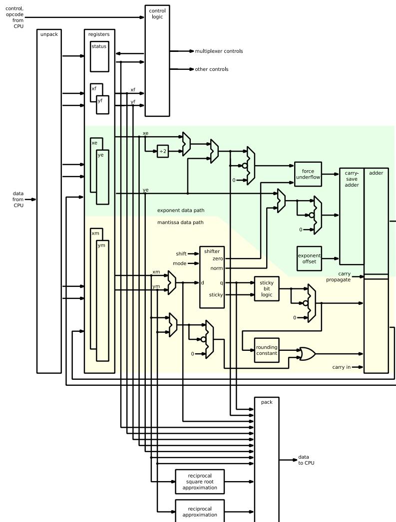
At the heart of the design are:
- • two sets of registers, each designed to hold an unpacked double-precision value
- • a 9-bit status register
Unlike a conventional FPU, the accelerator does not contain a full register bank. Not only does this save die area, it also means that saving and restoring the coprocessor's state is very fast: in fact, the entire state fits within six 32-bit words and hence can be saved to, or restored from, the CPU in three instructions.
The accelerator contains a wide adder, capable of adding two mantissa values and three exponent values simultaneously. There is also a shifter that can either perform a logical right shift by a given amount, or normalise a denormalised mantissa and report the amount of shift required to do so. A considerable amount of hardware in the shifter is shared between these two operating modes.
Control logic, shown at the top of the diagram, decodes coprocessor instructions and configures the accelerator's functional units and datapath multiplexers in order to execute the desired operation. Each coprocessor instruction takes a single cycle, so coprocessor operations cannot stall the CPU.
A floating-point operation such as addition or subtraction is carried out by executing a fixed (or 'canned') sequence of instructions as follows:
- 1. One or two MCRR instructions to write the operands to the coprocessor.
- 2. A number of CDP (and possibly other) instructions that together perform the operation itself.
- 3. An MRRC or MRC instruction to read back the result.
The hardware handles special cases involving zeroes, NaNs, and infinities, as well as rounding, underflow and overflow.
The accelerator does not contain a multiplier array, as that would occupy a considerable amount of die area. Instead, the mantissas of the operands of a multiplication operation are brought back into the CPU to take advantage of the fast long multiply instructions available there. The coprocessor handles the processing of exponents.
Division and square root operations also involve data moving back and forth between coprocessor and CPU. To assist with these operations, the coprocessor contains two small lookup tables (implemented as random logic) that provide initial approximations used in the divide and square root algorithms. The coprocessor handles the processing of exponents.
The accelerator is only meant to be used with the canned instruction sequences that implement basic floating-point operations. The state of the accelerator is not guaranteed to be preserved from the end of one canned sequence to the beginning of the next: see the discussion of the 'engaged' flag in the status register below.
3.6.2.3. Registers
X and Y mantissa registers
The X and Y mantissa registers ( xm and ym ) are each 64 bits wide. They can be read and written directly by the CPU; the xm register can also store the lower part of the result from the adder. When a value is written to the coprocessor using a 'write unpacked' MCRR instruction, the top two bits of the mantissa register are set to 01 and the next most significant bits are filled from the mantissa field of the floating-point operand. The low-order bits of the mantissa register are cleared.
X and Y exponent registers
The X and Y exponent registers ( xe and ye ) are each 14 bits wide. They can be read and written directly by the CPU; the xe register can also store the higher part of the result from the adder. When a value is written to the coprocessor using a 'write unpacked' MCRR instruction, the exponent register is set from the exponent field of the floating-point operand.
X and Y flag registers
The X and Y flag registers ( xf and yf ) are each four bits wide. They can be read and written directly by the CPU. The flag register stores information about the type of floating-point number represented in the corresponding mantissa and exponent registers: its sign, whether it is a zero, whether it is an infinity, and whether it is a NaN. When a value is written to the coprocessor using a 'write unpacked' MCRR instruction, the bits of the flag register are updated according to the type of the floating-point operand.
Status register
The status register contains nine bits. It can be read and written directly by the CPU. The least significant six bits of the register store the shift required to align the two operands of an addition or subtraction; the next two bits indicate whether the value represented by ( xe , xm ) is greater than, equal to, or less than the value represented by ( ye , ym ) - in other words, whether the magnitude of the value stored in the X registers is greater than, equal to, or less than the magnitude of the value stored in the Y registers. These status bits are set in the first step of an addition, subtraction or comparison operation after the operands have been loaded.
The final bit of the status register indicates whether the coprocessor is 'engaged'. The engaged flag is set by all coprocessor instructions that occur at the beginning or in the middle of the canned instruction sequences. It is cleared by those instructions used at the end of a canned sequence to read back a final result.
3.6.2.4. State save and restore
An interrupt handler can test the engaged flag to determine whether it has pre-empted an in-progress operation on the same coprocessor. If the engaged flag is set, the handler can save (and restore) the coprocessor state before using the coprocessor. If the engaged flag is clear, the save (and restore) step can be skipped. If this approach is implemented, the state of the accelerator must be regarded as undefined when not within one of the canned instruction sequences.
Three MRRC instructions are provided to copy the six words of state in the coprocessor into integer registers in the CPU, from where they can, for example, be pushed onto the stack. The last of these instructions clears the engaged flag.
Similarly, three MCRR instructions are provided to restore the state of the coprocessor from integer registers, including the state of the engaged flag.
3.6.2.5. Instruction summary
As mentioned above, it is intended that the coprocessor instructions are only used as part of canned sequences. Nevertheless, for completeness, a list of the available instructions is given here with an outline of their effects.
MCRR instructions are shown in Table 109 .
Table 109. MCRR instructions
| Mnemonic | Effect | Used by |
|---|---|---|
| WXMD | write xm direct | restore status |
| WYMD | write ym direct | restore status |
| WEFD | write xe , xf , ye , yf , other status direct | restore status |
| WXUP | write xm , xe , xf unpacked double-precision | double-precision binary operations |
| WYUP | write ym , ye , yf unpacked double-precision | double-precision binary operations |
| WXYU | write xm , xe , xf , ym , ye , yf two unpacked single-precision | single-precision binary operations |
| WXMS | write xm bit 0=0/1 if data zero/nonzero | dmul |
| WXMO | write xm direct OR into b0, add exponents, XOR signs | dmul |
| WXDD | write xm direct; subtract exponents, XOR signs | ddiv |
| WXDQ | write xm direct, offset exponent | dsqrt |
| WXUC | write X unsigned int+ \( 2^{52}+2^{32} \) , \( Y=2^{52}+2^{32} \) | conversions from unsigned int |
| WXIC | write X signed int+ \( 2^{52}+2^{32} \) , \( Y=2^{52}+2^{32} \) | conversions from signed int |
| WXDC | write X unpacked double-precision, \( Y=2^{52}+2^{32} \) | conversions from double-precision |
| WXFC | write X unpacked single-precision, \( Y=2^{52}+2^{32} \) | conversions from single-precision |
| WXFM | write xm direct, add exponents, XOR signs | fmul |
| WXFD | write xm direct, subtract exponents, XOR signs | fdiv |
| WXFQ | write xm direct, offset exponent | fsqrt |
CDP instructions are shown in Table 110 .
Table 110. CDP instructions
| Mnemonic | Effect | Used by |
|---|---|---|
| INIT | zero all registers | |
| ADD0 | compare X-Y , set status | add, sub, cmp |
| ADD1 | \( xm := \pm xm \pm \pm ym \gg s \) or \( \pm ym \pm \pm xm \gg s \) | add |
| SUB1 | \( xm := \pm xm - \pm ym \gg s \) or \( -\pm ym \pm \pm xm \gg s \) | sub |
| SQR0 | \( xe = xe/2 \) , \( xm = xm < 0:1 \) | sqrt |
| Mnemonic | Effect | Used by |
|---|---|---|
| NORM | normalise | |
| NRDF | normalise and round single-precision | single-precision operations, conversions to single-precision |
| NRDD | normalise and round double-precision | double-precision operations, conversions to double-precision |
| NTDC | normalise and truncate double-precision pre-integer conversion | truncating conversions to int |
| NRDC | normalise and round double-precision pre-integer conversion | rounding conversions to int |
MRRC and MRC instructions are shown in Table 111 .
Table 111. MRRC and MRC instructions
| Mnemonic | Effect | Used by |
|---|---|---|
| RXVD | read xf , VERSION direct | dclassify, check version |
| RCMP | read processed status | dcmp |
| RDFA | read FADD result packed from X | fadd |
| RDFS | read FSUB result packed from X | fsub |
| RDFM | read FMUL result packed from X | fmul |
| RDFD | read FDIV result packed from X | fdiv |
| RDFQ | read FSQRT result packed from X | fsqrt |
| RDFG | read general float result packed from X | double-precision to single-precision conversion |
| RDOC | read unsigned integer conversion result from X | conversions to unsigned int |
| RDIC | read signed integer conversion result from X | conversions to signed int |
| RXMD | read xm direct | save status |
| RYMD | read ym direct, engaged=0 | save status |
| REFD | read xe , xf , ye , yf , other status direct | save status |
| RXMS | read xm Q62-s | dmul, ddiv, dsqrt |
| RYMS | read ym Q62-s | dmul, ddiv |
| RXYH | read ym hi, xm hi | fmul, fdiv |
| RYMR | read ym hi, recip approximation lo | fdiv, ddiv |
| RXMQ | read xm hi, rsqrt approximation lo | fsqrt, dsqrt |
| RDDA | read DADD result packed from X | dadd |
| RDDS | read DSUB result packed from X | dsub |
| RDDM | read DMUL result packed from X | dmul |
| RDDD | read DDIV result packed from X | ddiv |
| Mnemonic | Effect | Used by |
|---|---|---|
| RDDQ | read DSQRT result packed from X | dsqrt |
| RDDG | read general double result packed from X | single-precision to double-precision conversion |
Alongside each MRRC and MRC instruction is a variant starting P (for 'peek') instead of R that has the same function but preserves the engaged flag. RXMD is identical to PXMD ; REFD is identical to PEFD .
The SDK includes macros to generate Arm assembler from the mnemonics above in the file
dcp_instr.inc.S
in the SDK, for example turning
WXUP r0,r1
into
mcrr p4,#1,r0,r1,c0
.
3.6.2.6. Example canned sequence
The assembly code sequence to implement a callable double-precision addition operation is shown in Table 112 .
Table 112. Assembly code sequence to implement a callable double-precision addition operation
| Arm assembler | Coprocessor mnemonic | Action |
|---|---|---|
mcrr p4,#1,r0,r1,c0 | WXUP r0,r1 | write R0 and R1 unpacked double-precision into X |
mcrr p4,#1,r2,r3,c1 | WYUP r2,r3 | write R2 and R3 unpacked double-precision into Y |
cdp p4,#0,c0,c0,c1,#0 | ADD0 | compare X and Y ; set status and alignment shift |
cdp p4,#1,c0,c0,c1,#0 | ADD1 | add/subtract (depending on status and signs) xm and ym aligned, write result to xm |
cdp p4,#8,c0,c0,c0,#1 | NRDD | normalise and round double-precision result |
mrcc p4,#1,r0,r1,c0 | RDDA r0,r1 | read R0 and R1 packed double-precision from X , including special-value processing for addition |
bx r14 | return from function |
Logic in the coprocessor ensures, for example, that the ADD1 instruction shifts the smaller argument, that xm and ym are negated as required before being sent to the adder, and that the larger exponent is used as the basis for the subsequent normalisation.
3.6.2.7. Using the coprocessor via the SDK library
The SDK
pico_double
library automatically uses the coprocessor for double-precision floating-point calculations. This is the simplest way to take advantage of the coprocessor, but it entails a few cycles of overhead for each operation. Not only is there the overhead involved in a function call and return, but for safety the general-purpose implementations in the SDK always test the engaged flag, saving and restoring the coprocessor state to and from the stack as needed. That ensures that the functions work correctly if used in interrupt handlers, without additional intervention.
3.6.2.8. Using the coprocessor directly
The SDK includes macros to generate canned sequences for standard operations in the file
dcp_canned.inc.S
in the SDK.
These allow the callable double-precision addition operation listed above, for example, to be written as:
dcp_dadd_m r0,r1, r0,r1,r2,r3 @ result in r0,r1; operands in r0,r1 and r2,r3
bx r14
dcp_dadd_m
is a macro which expands into the sequence of coprocessor instructions given above. This macro allows you to specify the integer registers to be used for the operands and the result, which means that using these macros directly not only avoids function call and return overhead, it also avoids the extra overhead associated with argument marshalling.
The more complex macros also require you to specify 'scratch' registers that they can use for storing intermediate results. The following function, which calculates the dot product of two three-element vectors of doubles pointed to by
R0
and
R1
, illustrates this:
push {r4-r9,r14}
ldrd r3,r4,[r0],#8           @ load x0
ldrd r5,r6,[r1],#8           @ load y0
dcp_dmul_m r7,r8, r3,r4,r5,r6, r3,r4,r5,r6,r12,r14,r9 @ compute x0y0 ①
ldrd r3,r4,[r0],#8           @ load x1
ldrd r5,r6,[r1],#8           @ load y1
dcp_dmul_m r3,r4, r3,r4,r5,r6, r3,r4,r5,r6,r12,r14,r9 @ compute x1y1 ①
dcp_dadd_m r7,r8, r3,r4,r7,r8 @ compute x0y0+x1y1
ldrd r3,r4,[r0],#8           @ load x2
ldrd r5,r6,[r1],#8           @ load y2
dcp_dmul_m r3,r4, r3,r4,r5,r6, r3,r4,r5,r6,r12,r14,r9 @ compute x2y2 ①
dcp_dadd_m r0,r1, r3,r4,r7,r8 @ compute x0y0+x1y1+x2y2 ②
pop {r4-r9,r15}- 1.
r3, r4, r5, r6, r12, r14, andr9are scratch registers. - 2. stores the result in
r0, r1.
NOTE
This example does not check the engaged flag. If used in interrupt handlers or in multi-threaded applications, a suitable test would have to be added. For example, see the
SDK implementation of
__aeabi_dadd
for an efficient way to do this. The test only needs to be performed once, at the beginning of the function, so the overhead in this case would be relatively small.
The following example demonstrates how to use the coprocessor:
Pico Examples: https://github.com/raspberrypi/pico-examples/blob/master/dcp/hello_dcp/hello_dcp.c Lines 18 - 109
18 extern double dcp_dot           (double*p, double*q, int n);
19 extern double dcp_dotx          (float*p, float*q, int n);
20 extern float  dcp_iirx          (float x, float*temp, float*coeff, int order);
21 extern void   dcp_butterfly_radix2 (double*x, double*y);
22 extern void   dcp_butterfly_radix2_twiddle_dif (double*x, double*y, double*tf);
23 extern void   dcp_butterfly_radix2_twiddle_dit (double*x, double*y, double*tf);
24 extern void   dcp_butterfly_radix4  (double*w, double*x, double*y, double*z);
25
26 static void dcp_test0() {
27     double u[3]={1,2,3};
28     double v[3]={4,5,6};
29     double w;
30     w=dcp_dot(u,v,3);
31     printf("(1,2,3).(4,5,6)=%g\n",w);
32 }
33
34 static void dcp_test1() {
35     float u[3]={1+pow(2,-20),2,3};
36     float v[3]={1-pow(2,-20),5,6};
37     double w;
38 w=dcp_dotx(u,v,3);| 3.6. Cortex-M33 coprocessors | 111 |
100     dcp_test1();
101     dcp_test2();
102     dcp_test3();
103     dcp_test4();
104     dcp_test5();
105     dcp_test6();
106
107     return 0;
108 }
There are also further examples in the
dcp/
directory in the
Pico Examples
repository.
3.6.2.9. IEEE 754 compliance
The canned instruction sequences provide IEEE-compliant operations with the exception that denormals are flushed to zero on input and output. Zeroes, NaNs and infinities are correctly handled. Rounding is to nearest, even on tie.
Faster versions of division and square root operations, named
ddiv_fast
and
dsqrt_fast
respectively, are available. These do not always give correctly rounded results but do have a guaranteed error before rounding of less than 0.5ulp ('units in last place'), which in particular means that if there is an exact representation of the result then that is what is returned.
3.6.2.10. Benchmarks
Table 113 gives cycle counts for various floating-point operations using the accelerator with inlined code, compared to some typical ranges of benchmarks for (a) fully-fledged hardware double-precision FPUs; and (b) pure software implementations.
Table 113. Cycle counts for floating-point operations using the accelerator
| Operation | Using coprocessor | Full hardware (latency) | Software only |
|---|---|---|---|
dadd | 6 | 2-6 | 70-90 |
dsub | 6 | 2-6 | 70-90 |
dmul | 17 | 3-7 | 75-90 |
ddiv | 51 | 13-60 | 135-600 |
ddiv_fast | 32 | ||
dsqrt | 49 | 15-62 | 130-650 |
dsqrt_fast | 38 | ||
dcmp | 4 | ||
dclassify | 2 | ||
integer to/from double | 5 |
3.6.3. Redundancy coprocessor (RCP)
Figure 13. The redundancy coprocessor implements hardware-checked assertions, to aid control flow and data flow integrity checking. Its two-phase pipeline is closely coupled to the Cortex-M33 pipeline. A 64-bit salt register holds a once-per-boot random number, which is used to generate and validate stack canary values and generate pseudorandom delay sequences on RCP instructions. Other comparison functions provide more general hardware-checked assertion support.
![Figure 13: Dataflow-level overview of the RCP hardware. The diagram shows a two-phase pipeline: Opcode Phase and Data Phase. In the Opcode Phase, CPOPC feeds into Instruction Decode, which outputs to Control Signals, Tag, and Decode Error. In the Data Phase, Tag feeds into Canary Generation, which outputs to CPRDATA[31:0]. CPRDATA[31:0] and CPWDATA[63:0] feed into Comparison. Comparison outputs to Fault Flag and a +1 block. Fault Flag feeds into Sequence Counter. Sequence Counter outputs to Fault Flag. The Salt Register is connected to CPRDATA[31:0] and CPWDATA[63:0].](/RP235x/7e12e1e0d03a03790d2e9d74c3454bff_img.jpg)
The redundancy coprocessor (RCP) is used in the RP2350 bootrom to provide hardware-assisted mitigation against fault injection and return-oriented programming attacks. This includes the following instructions:
- • generate and validate stack canary values based on a per-boot random seed
- • assert that certain points in the program are executed in the correct order without missing steps
- • validate booleans stored as one of two valid bit patterns in a 32-bit word
- • validate 32-bit integers stored redundantly in two words with an XOR parity mask
- • halt the processor upon reaching a software-detected panic condition
Section 3.6.3.7 lists the RCP instruction set in full. RCP instruction encodings contain a parity bit; executing an invalid instruction or an instruction with bad parity triggers an RCP fault.
Each Cortex-M33 processor is equipped with a single RCP instance, mapped as coprocessor number 7 in the coprocessor opcode space. The two RCP instances are linked: an RCP fault on one core immediately triggers a fault on the other. RCP faults have two steps:
- 1. The non-maskable interrupt (NMI) is asserted. It remains asserted until a warm reset of the processor.
- 2. Any further RCP instructions stall the coprocessor port until a warm reset of the processor. This stall cannot be interrupted, as the processor is already in the NMI state.
The RP2350 bootrom implements the NMI and HardFault vectors with an
rcp_panic
instruction. This instruction unconditionally stalls the coprocessor port. This prevents the processor from retiring any more instructions until either a debugger connects to reset the processors, or the processors reset through some other mechanism (such as the system watchdog timer). The processor quickly reaches a quiescent state that reduces vulnerability to further fault injection (deliberate or otherwise).
Each core's RCP has a 64-bit seed value (Section 3.6.3.1). The RCP uses this value to generate stack canary values and to add short pseudorandom delays to RCP instructions. Both RCP instances are seeded by core 0 during the early boot path in the bootrom using the system true-random number generator (Section 12.12). Running any RCP instruction before providing a salt value triggers an RCP fault. The use of random data in stack canary values makes it difficult to reuse return-oriented-programming stack payloads across multiple boots.
Figure 13 gives a dataflow-level overview of the RCP hardware. The RCP is structured as a two-phase pipeline which overlays the Cortex-M33 execution pipeline. It exchanges data with the core via a 64-bit incoming bus (CPWDATA) and a 32-bit outgoing bus (CPRDATA). The Cortex-M33 can issue two register reads to the coprocessor in one cycle through the CPWDATA bus. The RCP leverages this throughput for some of its assertion instructions, such as
rcp_inequal
, which raises a fault when two Arm registers do not contain the same 32-bit value.
The 8-bit tag value in Figure 13 is an 8-bit instruction immediate value encoded by the instruction CRn and CRm fields. These 8-bit values are used to uniquely identify functions for canary value generation so that stack frames are not interchangeable between functions. They also provide 8-bit counter values for rcp_count_set and rcp_count_check instructions. Encoding the tags using the CRn and CRm fields makes RCP instruction sequences more compact, as it obviates additional instructions to materialise these small constants in registers and pass them through CPWDATA. This also makes the tag values less vulnerable to glitching, because the instruction opcode fields are available earlier in the cycle than the register values passed on CPWDATA.
RCP instructions may also execute in the Non-secure state, with certain differences to prevent Non-secure code from triggering RCP faults or observing the value of the salt register. This supports Non-secure software executing shared ROM routines which contain RCP instructions, but does not allow probing of the RCP's internal state from a Non-secure context. Section 3.6.3.2 gives further details and rationale for Non-secure execution support.
Certain details are elided from Figure 13 for clarity, such as the delay counter used for pseudorandom instruction delays, and the logic for suppressing faults under Non-secure execution. This behaviour is described in full in the following sections.
3.6.3.1. Salt register
Each RCP instance is provisioned with a 64-bit salt register , which provides a seed for stack canary values and random instruction delays. This is expected to be initialised with a random value early in the boot process: the RP2350 bootrom uses the true random number generator to generate the salt values.
Initially the salt register is in the invalid state. This state only allows the following operations:
- • Checking the valid state of the salt register, via rcp_canary_status
- • Writing a salt via rcp_salt_core0 or rcp_salt_core1 , which writes a 64-bit value to that core's salt register, and changes its state to valid
When the salt register is in the invalid state, executing any RCP instruction other than those listed above unconditionally triggers an RCP fault . This makes it difficult to skip RCP initialisation via fault injection, because the RP2350 bootrom contains a high density of RCP instructions.
Similarly, attempting to write to an already-valid RCP salt register triggers an RCP fault. There is no reason to initialise the RCP salt register twice, so this case is detected as an anomaly that indicates loss of control flow integrity.
Core 0's coprocessor port writes the salt registers for both cores' RCP instances to simplify multicore interactions during early boot. In the RP2350 bootrom, core 1's first steps lock down its MPU execute permissions to a small region of the ROM containing its wait-for-launch code, and then poll for its RCP salt to become valid once core 0 has cleared boot memory, performed some minimal hardware setup, and generated the RCP salts.
When core 0 is switched to RISC-V architecture and core 1 is Arm, the core 1 salt register is forcibly marked as valid to permit core 1 to execute the ROM. This has no impact on secure boot because RISC-V cores are only enabled when secure boot is disabled; the ability to set core 0 to RISC-V already implies subversion of secure boot.
3.6.3.2. Access from Non-secure
Setting bit 7 of the Cortex-M33 NSACR register permits Non-secure code to set bit 7 of CPACR_NS , which in turn enables Non-secure access to the RCP. Non-secure RCP access is useful for executing shared Secure/Non-secure routines which contain RCP instructions. For example, the memcpy implementation in the RP2350 bootrom is shared by Secure code in the main boot path, and Non-secure code such as the USB bootloader.
Since an RCP fault is fatal for all software running on the system, Non-secure must not be able to trigger RCP faults at will. Similarly, if Non-secure code were able to read out the RCP salt register, it would make it easier to engineer stack payloads which can control Secure execution without triggering RCP faults. Therefore the RCP handles Non-secure accesses differently from Secure:
- • Masks read data to all-zeroes
- • Ignores write data: any instruction which would generate a data-dependent RCP fault becomes a no-op
- • Reports coprocessor errors instead of RCP faults for invalid instructions, which the processor maps to the Non-secure UNDEFINSTR UsageFault
- • Skips the pseudorandom instruction delay: all RCP instructions execute in one cycle, assuming the Cortex-M33 is able to issue them at one instruction per cycle
The lack of pseudorandom instruction delays makes it more difficult for Non-secure code to extract the seed value used to add delays to Secure execution of RCP instructions.
3.6.3.3. Instruction validation
The RCP applies the following rules to all coprocessor instructions which target coprocessor 7:
- • The number of 1 bits in the
Opc1field, plus the instruction parity bit, must be an even number.- ◦ For
mcr,mrcandcdpinstructions, bit 0 of theOpc2field encodes the parity bit. - ◦ For
mcr, bit 3 of theCRmfield encodes the parity bit.
- ◦ For
- • The instruction must not be an
mrrc(64-bit coprocessor-to-core) - • For
mcrinstructions (32-bit core-to-coprocessor):- ◦ The
Opc1field must be in the range 0 through 6. - ◦ If there is no 8-bit tag (i.e. any other than
rcp_canary_check,rcp_count_check,rcp_count_set), theCRnandCRmopcode fields must be all-zeroes.
- ◦ The
- • For
mrcinstructions (32-bit coprocessor-to-core):- ◦ The
Opc1field must be in the range 0 through 2. - ◦ For instructions other than
rcp_canary_getandrcp_canary_check, theCRnandCRmopcode fields must be all-zeroes.
- ◦ The
- • For
mrrcinstructions (64-bit core-to-coprocessor):- ◦ The
Opc1field must be in the range 0 through 8. - ◦ For
rcp_salt_core*instructions, bits 2:0 of theCRmfield must be 0 or 1 (referred to asrcp_salt_core0andrcp_salt_core1respectively). - ◦ For all other
mrrcinstructions, bits 2:0 of theCRmfield must be 0.
- ◦ The
The terms
Opc1
,
Opc2
,
CRm
and
CRn
in the description above refer to standard encoding fields in the Arm T32 instruction encoding for coprocessor instructions. See the
Arm v8-M Architecture Reference Manual
for full details of the encoding and assembler syntax.
Any coprocessor instruction targeting coprocessor 7 that fails these validation rules will result in one of two outcomes, depending on the security domain in which the instruction is executed:
- • Secure execution of an invalid instruction is an immediate, unconditional RCP fault. The RCP asserts the core's non-maskable interrupt signal, and any further RCP instructions stall the coprocessor port indefinitely. This continues until the core receives a warm reset. This also triggers RCP faults on other cores: for more information, see Section 3.6.3.4 .
- • Non-secure execution of an invalid instruction returns an error on the opcode-phase coprocessor interface, which is interpreted as a Non-secure UNDEFINSTR UsageFault by the core. For a full description of this Arm v8-M-specific fault, see the Arm v8-M Architecture Reference Manual .
3.6.3.4. Cross-core triggering
An RCP fault indicates that the integrity of the software environment is compromised. Though the fault may originate on
a single processor, all processors which share the same trusted memory may behave unpredictably if they continue to execute, since:
- • The physical condition which caused one processor to misexecute in a detectable way, such as low supply voltage, may cause other processors to misexecute in a manner which was not detected.
- • The processor which triggered an RCP fault may already have corrupted shared, trusted memory contents in a way that interferes with the other processor's operation, (e.g. corrupting the other core's stack).
Therefore, an RCP fault on one core also triggers an RCP fault on other cores. Because RP2350 has two cores, an RCP fault on core 0 always triggers a fault on core 1, and an RCP fault on core 1 always triggers a fault on core 0.
Figure 14. Triggering an RCP fault on one core also triggers a fault on the other core. Triggers accumulate into a fault register, which remains set until the core resets. The NMI asserts when the fault register is set.
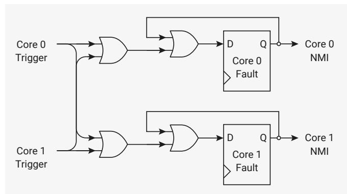
Each core locally ORs in the trigger signal from the other core. The outputs of the two OR gates on the left are logically equivalent, but the gates are kept local to the core to minimise delay routing the core's own fault trigger to its own fault register.
3.6.3.5. Stack canary values
Canaries are values written to the stack on function entry and validated on function exit, to assure that:
- • The exit matches the entry (i.e. when leaving through the back door, you entered through the front door)
- • The stack was not completely overwritten in the course of executing the function
This helps to mitigate two classes of attack:
- • Fault injection: any physical fault condition which corrupts the program counter or causes a wild indirect branch is likely to cause the processor to execute a function epilogue which does not match the prologue. Any branch into the middle of a function is likely to eventually reach the epilogue.
- • Return-oriented programming: deliberate stack corruption can redirect control flow through a sequence of function tails which perform arbitrary operations. The stack may be corrupted by exploiting missing bounds checks on stack buffer operations. Random canary values make it difficult to craft such a stack payload.
Return-oriented programming mitigation is particularly important to account for in the bootrom because the bootrom exposes an API surface that is mapped at a known location at runtime (it is physically always mapped at
0x00000000
). This provides a well-known exploit surface similar to the C standard library.
The RCP supports canary values with two canary-specific instructions:
- •
rcp_canary_getgenerates a 32-bit value for an 8-bit tag as a function of the salt register - •
rcp_canary_checkvalidates a 32-bit value for an 8-bit tag and raises an RCP fault if the value does not match that produced by anrcp_canary_getfor the same tag.
The 32-bit canary value is as follows:
- • Bits 7:0: all-zero
- • Bits 15:8: XOR of bits 7:0 of the salt with (AND of bits 31:24 of the salt with the 8-bit tag)
- • Bits 23:16: XOR of bits 15:8 of the salt with (AND of bits 39:32 of the salt with the bitwise NOT of the 8-bit tag)
- • Bits 31:24: XOR of bits 23:16 of the salt with the 8-bit tag
The following code demonstrates how you might calculate the 32-bit canary value in C:
uint32_t canary_value(uint64_t salt, uint8_t tag) {
    uint32_t tag_expanded =
        ((uint32_t)tag |
         ((uint32_t)~tag << 8)
         ((uint32_t)tag << 16));
    tag_expanded &= (0xff0000u | ((salt >> 24) & 0x00ffffu));
    uint32_t result24 = tag_expanded ^ salt;
    return result24 << 8;
}
This canary value is chosen such that:
- • Different tags are guaranteed to yield different canary values
- • For any two different tags, each is a function of at least one salt bit that the other is not a function of (so it is difficult to calculate canaries for different tags even if one value is known)
- • Null-terminated string operations on the stack terminate before reading or writing a canary
Each function should use a different canary tag, to prevent a stack frame for one function being used to return through another function's epilogue. Avoid using canary values for purposes other than stack canaries.
The RP2350 bootrom uses 8-bit tags in the range 0x40 through 0xbf. The remaining tags are free for use in user code.
3.6.3.6. Pseudorandom instruction delays
By default, all RCP instructions execute with a pseudorandom delay in the range of 0 to 127 cycles. These delays make it more difficult for an outside observer to precisely time a fault injection event with respect to an RCP instruction, or the critical code path it protects.
i NOTE
In certain usage situations, RCP delays can expose a side-channel where processor state can be inferred. See RP2350-E26 for details.
Setting bit 12 of the first halfword of an instruction disables the pseudorandom delay for that instruction only. The instruction executes in a single cycle, assuming the Cortex-M33 does not insert stall cycles due to other micro-architectural constraints. To set this bit, assemble the *2 variant of any given coprocessor instruction (e.g.
mrc2
rather than
mrc
). In the NonSecure state, RCP instructions always execute without delay.
The RCP implements instruction execution delays by stalling the coprocessor opcode interface during the opcode phase (shown in the Figure 13 pipeline diagram). The Cortex-M33 may choose to abandon a stalled coprocessor instruction due to an interrupt. When this happens, the delay counter continues counting down, waiting for the delay period to elapse. If the Cortex-M33 issues another RCP instruction whilst the delay counter is still running (either in the interrupt, or after returning to the interrupted RCP instruction), this instruction executes once the existing countdown completes. However, if the delay counter of an abandoned instruction has already expired before the next RCP instruction executes, the next instruction samples a pseudorandom delay count, and begins a new countdown.
The pseudorandom delay sequence is a function of bits 63:40 of the salt value. As such, the pattern of delays is unique per-boot, provided each boot writes a different 64-bit value to the salt register.
The pseudorandom number generator (PRNG) used for delays implements a number of small linear feedback shift registers (LFSRs) in bits 63:40 of the salt register, and returns a nonlinear function of the 24-bit state. The LFSR feedback functions on the 24-bit state are:
- • Bits 23:20: 4-bit LFSR with taps 0xc
- • Bits 19:15: 5-bit LFSR with taps 0x14
- • Bits 14:8: 7-bit LFSR with taps 0x60
- • Bits 7:0: 8-bit LFSR with taps 0xb4
The LFSRs are implemented by shifting the XOR reduction of (state AND taps) into the LSB with each state update. When an LFSR's state is all-zeroes, a one bit is shifted into the LSB. The LFSR state advances each time a random number is generated: this happens when executing an instruction with a pseudorandom delay, or when executing a
rcp_random_byte
instruction.
Each bit of the pseudorandom output is the XOR of six bits of the 24-bit state, XORed with the majority-3 vote of three other bits of the state:
| Output Bit | XOR Taps | Majority-3 Taps | |||||||
|---|---|---|---|---|---|---|---|---|---|
| 7 | 7 | 17 | 6 | 16 | 13 | 8 | 9 | 12 | 21 |
| 6 | 14 | 21 | 19 | 6 | 16 | 13 | 4 | 14 | 6 |
| 5 | 7 | 5 | 2 | 18 | 11 | 1 | 18 | 14 | 7 |
| 4 | 4 | 19 | 17 | 0 | 18 | 7 | 18 | 11 | 3 |
| 3 | 23 | 12 | 7 | 16 | 14 | 5 | 17 | 3 | 15 |
| 2 | 15 | 13 | 20 | 21 | 8 | 12 | 7 | 22 | 9 |
| 1 | 4 | 16 | 11 | 18 | 9 | 6 | 14 | 21 | 16 |
| 0 | 11 | 3 | 4 | 19 | 10 | 14 | 1 | 2 | 9 |
Bits 6:0 of this function are used for pseudorandom instruction delays, producing delays in the range of 0 to 127 cycles. The delay is applied in addition to the one-cycle base cost of executing a coprocessor instruction. The full 8-bit result is available through the
rcp_random_byte
instruction.
This is a simple pseudorandom number generator which makes it difficult to recover the initial 24-bit state from a small number of observations. It accomplishes this by making the observation size much smaller than the state size and using a non-linear combination function for the output. It has a number of statistical aberrations which make it unsuitable for general random number generation (not to mention its small state size). For high-quality random number generation, either use the system true-random number generator (TRNG) directly, or use a high-quality software PRNG with a large state seeded from the TRNG.
Note that the 24 MSBs of the salt value used to seed the delay PRNG do not overlap with the 40 LSBs used to generate stack canary values. Therefore measuring the random delays externally provides no information on the canary values.
3.6.3.7. Instruction listing
The Cortex-M33 processors access the RCP using
mcr
,
mcrf
,
mrc
, and
cdp
instructions. The
Armv8-M Architecture Reference Manual
describes the intricacies of these instructions in relation to the processor's architectural state, but from the coprocessor's point of view:
- •
mcrwrites a 32-bit value to the coprocessor from a single Arm integer register - •
mcrfwrites a 64-bit value to the coprocessor from a pair of Arm integer registers - •
mrcreads a 32-bit value from the coprocessor, writing to either a single Arm integer register or to the processor status flags - •
cdpperforms some internal coprocessor operation without exchanging data with the processor
For each
mcr
,
mcrf
,
mrc
and
cdp
instruction, the RCP also accepts the matching
mcr2
,
mcrf2
,
mrc2
, and
cdp2
opcode variant. These opcodes differ only in bit 12. The plain versions have a pseudorandom delay of up to 127 cycles on their
execution, whereas the 2 -suffixed versions have no such delay.
Most RCP instructions are in the form of hardware-checked assertions. The phrase "asserts that" in the following instruction listings means that, if some asserted condition is not true, the coprocessor raises an RCP fault.
3.6.3.7.1. Initialisation
rcp_salt_core0
Asserts that the core 0 salt register is currently invalid. Writes a 64-bit value, and marks it as valid.
Opcode:
mrrr p7, #8, Rt, Rt2, c0
Rt is the 32 LSBs of the salt, Rt2 is the 32 MSBs.
rcp_salt_core1
Asserts that the core 1 salt register is currently invalid. Writes a 64-bit value, and marks it as valid.
Opcode:
mrrr p7, #8, Rt, Rt2, c1
rcp_canary_status
Returns a true or false bit pattern ( 0xa500a500 or 0xc300c300 respectively) that indicates whether the salt register for this core has been initialised.
Opcode:
mrc p7, #1, Rt, c0, c0, #0
Invoking with Rt = 0xf sets the Arm N and C flags if and only if the salt register is valid.
If the salt has not been initialised, any operation other than initialising the salt or checking the canary status triggers an RCP fault.
This opcode is used on core 0 to skip the RCP initialisation sequence if the bootrom has been re-entered without a reset under debugger control, and on core 1 to wait for its RCP salt to be initialised.
3.6.3.7.2. Canary
rcp_canary_get
Gets a 32-bit canary value as a function of the salt register and the 8-bit tag encoded by two 4-bit coprocessor register numbers CRn and CRm . CRn contains the four MSBs, CRm the four LSBs.
Opcode:
mrc p7, #0, Rt, CRn, CRm, #1
Section 3.6.3.5
specifies the 32-bit value returned by this instruction, but you should treat this as an opaque value to be consumed by
rcp_canary_check
.
Asserts that a value matches the result of an
rcp_canary_get
with the same 8-bit tag. The tag is encoded by two 4-bit coprocessor register numbers,
CRn
and
CRm
.
CRn
contains the four MSBs,
CRm
the four LSBs.
Opcode:
mcr p7, #0, Rt, CRn, CRm, #13.6.3.7.3. Boolean validation
The RCP defines
0xa500a500
as the
true
value for 32-bit booleans, and
0x00c300c3
as the
false
value. All other bit patterns are poison, and trigger an RCP fault when consumed by any RCP boolean instructions. These values are chosen as they are valid immediates in Armv8-M Main.
This provides limited runtime type checking to ensure that boolean values are used in boolean contexts. The RP2350 bootrom occasionally uses redundant operations to generate booleans in a way that results in an invalid bit pattern if the two redundant operations do not return the same value, such as when checking boot flags in OTP.
rcp_bvalidAsserts that
Rt
is a valid boolean (
0xa500a500
or
0x00c300c3
).
Opcode:
mcr p7, #1, Rt, c0, c0, #0rcp_btrue
Asserts that
Rt
is
true
(
0xa500a500
).
Opcode:
mcr p7, #2, Rt, c0, c0, #0rcp_bfalse
Asserts that
Rt
is
false
(
0x00c300c3
).
Opcode:
mcr p7, #3, Rt, c0, c0, #1rcp_b2valid
Asserts that
Rt
and
Rt2
are both valid booleans.
Opcode:
mcr p7, #0, Rt, Rt2, c8rcp_b2and
Asserts that Rt and Rt2 are both true .
Opcode:
mrrr p7, #1, Rt, Rt2, c0rcp_b2or
Asserts that both Rt and Rt2 are valid, and at least one is true .
mrrr p7, #2, Rt, Rt2, c0rcp_bxorvalid
Asserts that Rt XOR Rt2 is a valid boolean. The XOR mask is generally a fixed bit pattern used to validate the origin of the boolean, such as a return value from a critical function.
Opcode:
mrrr p7, #3, Rt, Rt2, c8rcp_bxortrue
Asserts that Rt XOR Rt2 is true .
Opcode:
mrrr p7, #4, Rt, Rt2, c0rcp_bxorfalse
Asserts that Rt XOR Rt2 is false .
Opcode:
mrrr p7, #5, Rt, Rt2, c83.6.3.7.4. Integer Validation rcp_ivalid
Asserts that Rt XOR Rt2 is equal to 0x96009600 . This is used to validate 32-bit integers stored redundantly in two memory words. The XOR difference provides assurance that two parallel chains of integer operations have not mixed.
Opcode:
mcr p7, #6, Rt, Rt2, c8
rcp_inequal
Asserts that Rt is equal to Rt2 . Useful for general software assertions that are worth checking in hardware.
Opcode:
mcr p7, #7, Rt, Rt2, c0
3.6.3.7.5. Random
rcp_random_byte
Returns a random 8-bit value generated from the upper 24 bits of the 64-bit salt value. Bits 31:8 of the result are all-zero.
Opcode:
mrc p7, #2, Rt, c0, c0, #0
This is the same PRNG used for random delay values. It is mainly exposed for debugging purposes, and should not be used for general software RNG purposes because the 24-bit state space is inadequate for scenarios where the quality and predictability of the random numbers is important.
This instruction never has an execution delay. Once the Cortex-M33 issues the coprocessor access, it always completes in one cycle.
3.6.3.7.6. Sequence count checking
These instructions are used to assert that a sequence of operations happens in the correct order. The count is initialised to an 8-bit value at the beginning of such a sequence, then repeatedly checked, incrementing with each check. If the 8-bit check value does not match the current counter value, the coprocessor raises an RCP fault.
rcp_count_set
Writes an 8-bit count value to the RCP sequence counter. Encodes the 8-bit value using two 4-bit coprocessor numbers: CRn provides the MSBs, CRm the LSBs.
Opcode:
mcr p7, #4, r0, CRn, CRm, #0
rcp_count_check
Asserts that an 8-bit count value matches the current value of the RCP sequence counter. Increments the counter by one, wrapping back to 0x00 after reaching 0xff . Encodes the 8-bit count value using two 4-bit coprocessor numbers: CRn provides the MSBs, CRm the LSBs.
Opcode:
mcr p7, #5, r0, CRn, CRm, #1
3.6.3.7.7. Panic
rcp_panic
Stalls the coprocessor port forever. If the processor abandons the coprocessor access, asserts NMI and continues stalling the coprocessor port. Also immediately raises an RCP fault on other cores.
Opcode:
cdp p7, #0, c0, c0, c0, #1
Software executes an
rcp_panic
instruction when it detects a condition that makes it unsafe to continue executing the current program. The RCP responds by stalling the processor's CDP access forever, which should cause the processor to stop fetching and executing instructions.
The processor is allowed to abandon a stalled coprocessor instruction when interrupted, which may cause it to continue executing in an unsafe state. The RCP responds to an abandoned transfer by asserting the non-maskable interrupt, pre-empting the interrupt handler that caused the coprocessor access to be abandoned. This should swiftly encounter another RCP instruction and once again stall the processor, this time without allowing interruption.
Panic is specified in this way, instead of gating the processor clock, so the debugger can still attach cleanly to the processor after a panic.
3.6.4. Floating point unit
The Cortex-M33 cores on RP2350 are configured with the standard Arm single-precision floating point unit (FPU). Coprocessor ports 10 and 11 access the FPU.
The Arm floating point extension is documented in the Armv8-M Architecture Reference Manual .
Applications built with the SDK use the FPU automatically by default. For example, calculations with the
float
data type in C automatically use the standard FPU, while calculations with the
double
data type automatically use the RP2350 double-precision coprocessor (
Section 3.6.2
).
3.7. Cortex-M33 processor
Arm Documentation
Much of the following is excerpted from the Cortex-M33 Technical Reference Manual . Used with permission.
The Arm Cortex-M33 processor is a low gate count, highly energy-efficient processor intended for microcontroller and embedded applications. The processor is based on the Armv8-M architecture and is primarily for use in environments where security is an important consideration.
NOTEFull details of the Arm Cortex-M33 processor can be found in the Technical Reference Manual .
3.7.1. Features
The Arm Cortex-M33 processor provides the following features and benefits:
- • An in-order issue pipeline
- • Thumb-2 technology; for more information, see the Armv8-M Architecture Reference Manual
- • Little-endian data accesses
- • A Nested Vectored Interrupt Controller (NVIC) closely integrated with the processor
- • A Floating Point Unit (FPU) supporting single-precision arithmetic
- • Support for exception-continuable instructions, such as LDM, LDMDB, STM, STMDB, PUSH, POP, VLDM, VSTM, VPUSH, and VPOP
- • A low-cost debug solution that provides the ability to implement:
- ◦ Breakpoints
- ◦ Watchpoints
- ◦ Tracing
- ◦ System profiling
- ◦ Support for
printf()style debugging through an Instrumentation Trace Macrocell (ITM)
- • Support for the Embedded Trace Macrocell (ETM) instruction trace option; for more information, see the Arm CoreSight ETM-M33 Technical Reference Manual
- • A coprocessor interface for external hardware accelerators
- • Low-power features including architectural clock gating, sleep mode, and a power-aware system with Wake-up Interrupt Controller (WIC)
- • A memory system that includes memory protection and security attribution
3.7.2. Configuration
Each Arm Cortex-M33 processor in RP2350 is configured with the following features:
- • FPU : Single precision FPU
- • DSP : DSP extension
- • SECEXT : Security extensions
- • CPIF : coprocessor interface
- • MPU_NS : 8 non-secure MPU regions
- • MPU_S : 8 secure MPU regions
- • SAU : 8 SAU regions
- • IRQ : 52 external interrupts
- • IRQLVL : 4 exception priority bits
- • DBGLVL : Full debug set: 4 watchpoint, 8 breakpoint comparators, debug monitor
- • ITM: DWT and ITM trace
- • ETM : ETM trace
- • MTB : no MTB trace
- • WIC: Wake up interrupt controller
- • WICLINES: 55: All external interrupts and 3 internal events: NMI, RVEX, Debug
- • CTI : Cross trigger interface
- • RAR: reset all registers on power up
- • UNCROSS_I_D : Modify internal address map
- • SBIST: no SBIST features
- • CDE modules not used
- • CDERTLID: RTL ID for system with multi Cortex-M33: 16
Architectural clock gating allows the processor core to support SLEEP and DEEPSLEEP power states by disabling the clock to parts of the processor core. Power gating is not supported.
Each Cortex-M33 core has its own interrupt controller that can individually mask out interrupt sources as required. The same interrupts route to both Cortex-M33 cores.
The processor supports the following interfaces:
- • Code AHB (C-AHB) interface
- • System AHB (S-AHB) interface
- • External PPB (EPPB) APB interface
- • Debug AHB (D-AHB) interface
The processor implements the following optional interfaces:
- • Arm TrustZone technology, using the Armv8-M Security Extension supporting Secure and Non-secure states
- • Memory Protection Units (MPUs), which you can configure to protect regions of memory
- • Floating-point arithmetic functionality with support for single precision arithmetic
- • Support for ETM trace
3.7.2.1. Modifications by Raspberry Pi
3.7.2.1.1. UNCROSS_I_D
The original Cortex-M33 processor design routes the following operations to either the Code or System port:
- • instruction fetch
- • load/stores
- • debugger accesses
Accesses below address 0x20000000 route to the Code port. All other accesses route to the System port.
This routing strategy makes contention possible on both the internal bus matrix and the main system AHB5 crossbar. The Cortex-M33 Technical Reference Manual describes this strategy in detail.
In RP2350, Raspberry Pi modified the Cortex-M33 bus matrix to:
- • route all instruction fetch operations to the Code port
- • route all load/stores and debugger accesses to the System port
This eliminates internal conflicts and improves performance in certain software use cases, e.g. when allocating both code and data from a single unified SRAM pool.
In
Section 3.7.2
, we refer to this feature as
UNCROSS_I_D
.
There are no other modifications to the Cortex-M33 processor.
NOTE
This datasheet may refer to the Cortex-M33 Code and System ports as the instruction and data ports respectively (I and D), to reflect this modification to the core's integrated bus matrix.
3.7.2.2. Interfaces
The processor has various external interfaces:
Code and System AHB interfaces
Harvard AHB bus architecture supporting exclusive transactions and security state.
System AHB interface
The System AHB (S-AHB) interface is used for any instruction fetch and data access to the memory-mapped SRAM, Peripheral, External RAM and External device, or Vendor_SYS regions of the Armv8-M memory map.
Code AHB interface
The Code AHB (C-AHB) interface is used for any instruction fetch and data access to the Code region of the Armv8-M memory map.
External Private Peripheral Bus
The External PPB (EPPB) APB interface enables access to CoreSight-compatible debug and trace components in a system connected to the processor.
Secure attribution interface
The processor has an interface that connects to an external Implementation Defined Attribution Unit (IDAU), which enables your system to set security attributes based on address.
ATB interfaces
The ATB interfaces output trace data for debugging. The ATB interfaces are compatible with the CoreSight architecture. See the Arm CoreSight Architecture Specification v2.0 for more information. The instruction ATB interface is used by the ETM, and the instrumentation ATB interface is used by the Instrumentation Trace Macrocell (ITM).
Micro Trace Buffer interfaces
The Micro Trace Buffer (MTB) AHB slave interface and SRAM interface are for the CoreSight Micro Trace Buffer.
Coprocessor interface
The coprocessor interface is designed for closely coupled external accelerator hardware.
Debug AHB interface
The Debug AHB (D-AHB) slave interface allows a debugger access to registers, memory, and peripherals. The D-AHB interface provides debug access to the processor and the complete memory map.
Cross Trigger Interface
The processor includes a Cross Trigger Interface (CTI) Unit that has an interface that is suitable for connection to external CoreSight components using a Cross Trigger Matrix (CTM).
Power control interface
The processor supports a number of internal power domains that can be enabled and disabled using Q-channel interfaces connected to a Power Management Unit (PMU) in the system.
3.7.2.3. Security attribution and memory protection
The Cortex-M33 processor supports the Armv8-M Protected Memory System Architecture (PMSA) that provides programmable support for memory protection using a number of software controllable regions. RP2350 supports 8 programmable regions.
PMSA allows privileged software to assign access permissions to a memory region. When unprivileged software attempts to access the region, a fault exception is triggered. PMSA includes fault status registers that allow an exception handler to determine the source of the fault, apply corrective action, and notify the system. This reduces the potential impact of incorrectly-written application code.
The Cortex-M33 processor also includes support for defining memory regions as Secure or Non-secure, as defined in the Armv8-M Security Extension. This protects memory regions from accesses with an inappropriate level of security.
3.7.2.4. Floating-point unit (FPU)
The FPU provides:
- • Instructions for single-precision (C programming language float type) data-processing operations
- • Instructions for double-precision (C programming language double type) load and store operations
- • Combined multiply-add instructions for increased precision (Fused MAC)
- • Hardware support for conversion, addition, subtraction, multiplication, accumulate, division, and square-root
- • Hardware support for denormals and all IEEE Standard 754-2008 rounding modes
- • Thirty-two 32-bit single-precision registers or sixteen 64-bit double-precision registers
- • Lazy floating-point context save
3.7.2.4.1. Lazy floating-point context save
This FPU function delays automated stacking of floating-point state until the ISR attempts to execute a floating-point instruction. This reduces the latency to enter the ISR and removes floating-point context save for ISRs that do not use floating-point.
3.7.2.5. NVIC
The Nested Vectored Interrupt Controller NVIC prioritizes external interrupt signals. Software can set the priority of each interrupt. The NVIC and the Cortex-M33 processor core are closely coupled, providing low latency interrupt processing and efficient processing of late arriving interrupts.
i NOTE
"Nested" refers to the fact that interrupts can themselves be interrupted, by higher-priority interrupts. "Vectored" refers to the hardware dispatching each interrupt to a distinct handler routine specified by a vector table. For more details about nesting and vectoring behaviour, see the Armv8-M Architecture Reference Manual .
All NVIC registers are only accessible using word transfers. Any attempt to read or write a halfword or byte individually is unpredictable.
NVIC registers are always little-endian.
The Nested Vectored Interrupt Controller (NVIC) is closely integrated with the core to achieve low-latency interrupt processing.
Functions of the NVIC include:
- • External interrupts, configurable from 1 to 480 using a contiguous or non-contiguous mapping. This is configured at implementation.
- • Configurable levels of interrupt priority from 8 to 256. This is configured at implementation.
- • Dynamic reprioritisation of interrupts.
- • Priority grouping. This enables selection of pre-empting interrupt levels and non-pre-empting interrupt levels.
- • Support for tail-chaining and late arrival of interrupts. This enables back-to-back interrupt processing without the overhead of state saving and restoration between interrupts.
- • Support for the Armv8-M Security Extension. Secure interrupts can be prioritized above any Non-secure interrupt.
3.7.2.6. Cross Trigger Interface Unit (CTI)
The CTI enables the debug logic, MTB, and ETM to interact with each other and with other CoreSight™ components.
3.7.2.7. ETM
The ETM provides instruction-only capabilities.
3.7.2.8. MTB
The MTB provides a simple low-cost execution trace solution for the Cortex-M33 processor.
Trace is written to an SRAM interface, and can be extracted using a dedicated AHB slave interface (M-AHB) on the processor. The MTB can be controlled by memory-mapped registers in the PPB region or by events generated by the DWT or through the CTI.
See the Arm CoreSight MTB-M33 Technical Reference Manual for more information.
3.7.2.9. Debug and trace
Debug and trace components include a configurable Breakpoint Unit (BPU) used to implement breakpoints and a configurable Data Watchpoint and Trace (DWT) unit used to implement watchpoints, data tracing, and system profiling. Other debug and trace components include:
- • ITM for support of
printf()style debugging, using instrumentation trace - • Interfaces suitable for:
- ◦ Passing on-chip data through a Trace Port Interface Unit (TPIU) to a Trace Port Analyzer (TPA) via a 4-bit DDR output selected as a GPIO function (see Section 3.5.7 )
- ◦ A ROM table to allow debuggers to determine which components are implemented in the Cortex-M33 processor
- ◦ Debugger access to all memory and registers in the system, including access to memory-mapped devices, access to internal core registers when the core is halted, and access to debug control registers even when reset is asserted
3.7.3. Compliance
The processor complies with, or implements, the relevant Arm architectural standards and protocols, and relevant external standards.
3.7.3.1. Arm architecture
The processor is compliant with the following:
- • Armv8-M Main Extension
- • Armv8-M Security Extension
- • Armv8-M Protected Memory System Architecture (PMSA)
- • Armv8-M Floating-point Extension
- • Armv8-M Digital Signal Processing (DSP) Extension
- • Armv8-M Debug Extension
- • Armv8-M Flash Patch Breakpoint (FPB) architecture version 2.0
3.7.3.2. Bus architecture
The processor provides external interfaces that comply with the AMBA 5 AHB5 protocol. The processor also implements interfaces for CoreSight and other debug components using the APB4 protocol and ATBv1.1 part of the AMBA 4 ATB protocol.
For more information, see the:
- • Arm AMBA 5 AHB Protocol Specification
- • AMBA APB Protocol Version 2.0 Specification
- • Arm AMBA 4 ATB Protocol Specification ATBv1.0 and ATBv1.1
The processor also provides a Q-Channel interface. For more information, see the AMBA Low Power Interface Specification .
3.7.3.3. Debug
The debug features of the processor implement the Arm Debug Interface Architecture. For more information, see the Arm Debug Interface Architecture Specification, ADIv5.0 to ADIv5.2 .
3.7.3.4. Embedded Trace Macrocell
The trace features of the processor implement the Arm Embedded Trace Macrocell (ETM) v4.2 architecture.
For more information, see the Arm CoreSight ETM-M33 Technical Reference Manual .
3.7.3.5. Floating-point unit
The Cortex-M33 processor with FPU supports single-precision arithmetic as defined by the FPv5 architecture that is part of the Armv8-M architecture. The FPU provides floating-point computation functionality compliant with ANSI/IEEE Standard 754-2008, IEEE Standard for Binary Floating-Point Arithmetic.
The FPU supports single-precision add, subtract, multiply, divide, multiply and accumulate, and square root operations. It also provides conversions between fixed-point and floating-point data formats, and floating-point constant instructions.
The FPU provides an extension register file containing 32 single-precision registers.
The registers can be viewed as:
- • Thirty-two 32-bit single-word registers, S0-S31
- • Sixteen 64-bit double-word registers, D0-D15
- • A combination of registers from these views
3.7.3.5.1. FPU modes
The FPU provides full-compliance, flush-to-zero, and Default NaN modes of operation. In full-compliance mode, the FPU processes all operations according to the IEEE 754 standard in hardware.
Modes of operation are controlled using the Floating-Point Status and Control Register, FPSCR .
Setting the FPSCR.FZ bit enables Flush-to-Zero (FZ) mode. In FZ mode, the FPU treats all subnormal input operands of arithmetic operations as zeros. Exceptions that result from a zero operand are signalled appropriately. VABS , VNEG , and VMOV are not considered arithmetic operations and are not affected by FZ mode. When an operation yields a tiny result (as described in the IEEE 754 standard, where the destination precision is smaller in magnitude than the minimum normal value before rounding) FZ mode replaces the result with a zero.
The FPSCR.IDC bit indicates when an input flush occurs.
The FPSCR.UFC bit indicates when a result flush occurs.
Setting the FPSCR.DN bit enables Default NaN (DN) mode. In NaN mode, the result of any arithmetic data processing operation that involves an input NaN, or that generates a NaN result, returns the default NaN. All arithmetic operations except for VABS , VNEG , and VMOV ignore the fraction bits of an input NaN.
Setting neither the FPSCR.DN bit nor the FPSCR.FZ bit enables full-compliance mode. In full-compliance mode, FPv5 functionality is compliant with the IEEE 754 standard in hardware.
For more information about the FPU and FPSCR , see the Armv8-M Architecture Reference Manual .
3.7.3.5.2. FPU exceptions
The FPU sets the cumulative exception status flag in the FPSCR register as required for each instruction, in accordance with the FPv5 architecture. The FPU does not support exception traps.
The processor has six output pins. By default, they are disconnected. Each reflect the status of one of the cumulative exception flags:
FPIXC
Masked floating-point inexact exception.
FPUFC
Masked floating-point underflow exception.
FPOFC
Masked floating-point overflow exception.
FPDZC
Masked floating-point divide by zero exception.
FPIDC
Masked floating-point input denormal exception.
FPIOC
Invalid operation.
When a floating-point context is active, the stack frame extends to accommodate the floating-point registers. To reduce the additional interrupt latency associated with writing the larger stack frame on exception entry, the processor supports lazy stacking. This means that the processor reserves space on the stack for the FP state, but does not save that state information to the stack unless the processor executes an FPU instruction inside the exception handler.
The lazy save of the FP state is interruptible by a higher priority exception. The FP state saving operation starts over after that exception returns.
3.7.3.5.3. Low power FPU operation
If the FPU is in a separate power domain, the way the FPU domain powers down depends on whether the FPU domain includes state retention logic.
To power down the FPU:
- • If FPU domain includes state retention logic, disable the FPU by clearing the
CPACR.CP10andCPACR.CP11bitfields. - • If FPU domain does not include state retention logic, disable the FPU by clearing the
CPACR.CP10andCPACR.CP11bitfields and set both theCPPWR.SU10andCPPWR.SU11bitfields to 1.
 WARNING
Setting the
CPPWR.SU10
and
CPPWR.SU11
bitfields indicates that FPU state can be lost.
3.7.4. Programmer's model
The Cortex-M33 programmer's model is an implementation of the Armv8-M Main Extension architecture.
For a complete description of the programmers model, refer to the Armv8-M Architecture Reference Manual , which also contains the Armv8-M Thumb instructions. In addition, other options of the programmers model are described in the System Control, MPU, NVIC, FPU, Debug, DWT, ITM, and TPIU feature topics.
3.7.4.1. Modes of operation and execution
The Cortex-M33 processor supports Secure and Non-secure security states, Thread and Handler operating modes, and can run in either Thumb or Debug operating states. In addition, the processor can limit or exclude access to some resources by executing code in privileged or unprivileged mode.
See the Armv8-M Architecture Reference Manual for more information about the modes of operation and execution.
3.7.4.1.1. Security states
With the Armv8-M Security Extension, the programmer's model includes two orthogonal security states: Secure state and Non-secure state. The processor always resets into Secure state. Each security state includes a set of independent operating modes and supports both privileged and unprivileged user access. Registers in the System Control Space are banked across Secure and Non-secure state, with a Non-secure register view available to Secure state at an aliased address.
3.7.4.1.2. Operating modes
For each security state, the processor can operate in Thread or Handler mode. The following conditions cause the processor to enter Thread or Handler mode:
- • The processor enters Thread mode on reset, or as a result of an exception return to Thread mode. Privileged and Unprivileged code can run in Thread mode.
- • The processor enters Handler mode as a result of an exception. In Handler mode, all code is privileged.
The processor can change security state on taking an exception, for example when a Secure exception is taken from Non-secure state, the Thread mode enters the Secure state Handler mode. The processor can also call Secure functions
from Non-secure state and Non-secure functions from Secure state. The Security Extension includes requirements for these calls to prevent Secure data from being accessed in Non-secure state.
3.7.4.1.3. Operating states
The processor can operate in Thumb or Debug state:
- • Thumb state is the state of normal execution running 16-bit and 32-bit halfword- aligned Thumb instructions.
- • Debug state is the state when the processor is in Halting debug.
3.7.4.1.4. Privileged access and unprivileged user access
Code can execute as privileged or unprivileged. Unprivileged execution limits resource access appropriate to the current security state. Privileged execution has access to all resources available to the security state. Handler mode is always privileged. Thread mode can be privileged or unprivileged.
3.7.4.2. Instruction set summary
The processor implements the following instruction from Armv8-M:
- • All base instructions
- • All instructions in the Main Extension
- • All instructions in the Security Extension
- • All instructions in the DSP Extension
- • All single-precision instructions and double precision load/store instructions in the Floating-point Extension
For more information about Armv8-M instructions, see the Armv8-M Architecture Reference Manual .
3.7.4.3. Memory model
The processor contains a bus matrix that arbitrates instruction fetches and memory accesses from the processor core between the external memory system and the internal System Control Space (SCS) and debug components.
Priority is usually given to the processor to keep debug accesses as non-intrusive as possible.
The system memory map is Armv8-M Main Extension compliant, and is common both to the debugger and processor accesses.
The default memory map provides user and privileged access to all regions except for the Private Peripheral Bus (PPB). The PPB space only allows privileged access.
The following table shows the default memory map. This is the memory map used when the included MPUs are disabled. The attributes and permissions of all regions, except that targeting the NVIC and debug components, can be modified using an implemented MPU.
Table 114. Default memory map
| Address Range (inclusive) | Region | Interface |
|---|---|---|
| 0x00000000 - 0x1FFFFFFF | Code | Instruction and data accesses. |
| 0x20000000 - 0x3FFFFFFF | SRAM | Instruction and data accesses. |
| 0x40000000 - 0x5FFFFFFF | Peripheral | Instruction and data accesses. Any attempt to execute instructions from the peripheral and external device region results in a MemManage fault. |
| Address Range (inclusive) | Region | Interface |
|---|---|---|
| 0x60000000 - 0x9FFFFFFF | External RAM | Instruction and data accesses. Any attempt to execute instructions from the peripheral and external device region results in a MemManage fault. |
| 0xA0000000 - 0xDFFFFFFF | External device | Instruction and data accesses. Any attempt to execute instructions from the peripheral and external device region results in a MemManage fault. |
| 0xE0000000 - 0xE00FFFFF | PPB | Reserved for system control and debug. Cannot be used for exception vector tables. Data accesses are either performed internally or on EPPB. Accesses in the range 0xE0000000 - 0xE0043FFF are handled within the processor. Accesses in the range 0xE0044000 - 0xE00FFFFF appear as APB transactions on the EPPB interface of the processor. Any attempt to execute instructions from the region results in a MemManage fault. |
| 0xE0100000 - 0xFFFFFFFF | Vendor_SYS | Partly reserved for future processor feature expansion. Any attempt to execute instructions from the region results in a MemManage fault. |
The internal Secure Attribution Unit (SAU) determines the security level associated with an address. Some internal peripherals have memory-mapped registers in the PPB region which are banked between Secure and Non-secure state. When the processor is in Secure state, software can access both the Secure and Non-secure versions of these registers. The Non-secure versions are accessed using an aliased address.
For more information about the memory model, see the Armv8-M Architecture Reference Manual .
3.7.4.3.1. Private Peripheral Bus (PPB)
The Private Peripheral Bus (PPB) memory region provides access to internal and external processor resources.
The internal PPB provides access to:
- • The System Control Space (SCS), including the Memory Protection Unit (MPU), Secure Attribution Unit (SAU), and the Nested Vectored Interrupt Controller (NVIC).
- • The Data Watchpoint and Trace (DWT) unit.
- • The Breakpoint Unit (BPU).
- • The Embedded Trace Macrocell (ETM).
- • CoreSight Micro Trace Buffer (MTB).
- • Cross Trigger Interface (CTI).
- • The ROM table.
The external PPB (EPPB) provides access to implementation-specific external areas of the PPB memory map.
3.7.4.3.2. Unaligned accesses
The Cortex-M33 processor supports unaligned accesses. They are converted into two or more aligned AHB transactions on the C-AHB or S-AHB master ports on the processor.
Unaligned support is only available for load/store singles (LDR, LDRH, STR, STRH, TBH) to addresses in Normal memory. Load/store double and load/store multiple instructions already support word aligned accesses, but do not permit other unaligned accesses, and generate a fault if this is attempted. Unaligned accesses in Device memory are not permitted and fault. Unaligned accesses that cross memory map boundaries are architecturally UNPREDICTABLE .
NOTE
If
CCR.UNALIGN_TRP
for the current Security state is set, any unaligned accesses generate a fault.
3.7.4.4. Exclusive monitor
The Cortex-M33 processor implements a local exclusive monitor. The local monitor within the processor has been constructed so that it does not hold any physical address, but instead treats any store-exclusive access as matching the address of the previous load-exclusive. This means that the implemented exclusives reservation granule is the entire memory address range. For more information about semaphores and the local exclusive monitor, see the Armv8-M Architecture Reference Manual .
3.7.4.5. Processor core registers summary
The following table shows the processor core register set summary. Each of these registers is 32 bits wide. When the Armv8-M Security Extension is included, some of the registers are banked. The Secure view of these registers is available when the Cortex-M33 processor is in Secure state and the Non-secure view when Cortex-M33 processor is in Non-secure state.
Table 115. Processor core register set summary
| Name | Description |
|---|---|
| R0-R12 | R0-R12 are general-purpose registers for data operations. |
| MSP (R13) | The Stack Pointer (SP) is register R13. In Thread mode, the CONTROL register indicates the stack pointer to use, Main Stack Pointer (MSP) or Process Stack Pointer (PSP). There are two MSP registers in the Cortex-M33 processor: MSP_NS for the Non-secure state, and MSP_S for the Secure state. |
| PSP (R13) | The Stack Pointer (SP) is register R13. In Thread mode, the CONTROL register indicates the stack pointer to use, Main Stack Pointer (MSP) or Process Stack Pointer (PSP). There are two PSP registers in the Cortex-M33 processor: PSP_NS for the Non-secure state, and PSP_S for the Secure state. |
| MSPLIM | The stack limit registers limit the extent to which the MSP and PSP registers can descend respectively. There are two MSPLIM registers in the Cortex-M33 processor: MSPLIM_NS for the Non-secure state, and MSPLIM_S for the Secure state. |
| PSPLIM | The stack limit registers limit the extent to which the MSP and PSP registers can descend respectively. There are two PSPLIM registers in the Cortex-M33 processor: PSPLIM_NS for the Non-secure state, and PSPLIM_S for the Secure state. |
| LR (R14) | The Link Register (LR) is register R14. It stores the return information for subroutines, function calls, and exceptions. |
| PC (R15) | The Program Counter (PC) is register R15. It contains the current program address. |
| Name | Description |
|---|---|
| PSR | The Program Status Register (PSR) combines the Application Program Status Register (APSR), Interrupt Program Status Register (IPSR), and Execution Program Status Register (EPSR). These registers provide different views of the PSR. |
| PRIMASK | The PRIMASK register prevents activation of exceptions with configurable priority. When the Armv8-M Security Extension is included, there are two PRIMASK registers in the Cortex-M33 processor: PRIMASK_NS for the Non-secure state and PRIMASK_S for the Secure state. |
| BASEPRI | The BASEPRI register defines the minimum priority for exception processing. There are two BASEPRI registers in the Cortex-M33 processor: BASEPRI_NS for the Non-secure state, and BASEPRI_S for the Secure state. |
| FAULTMASK | The FAULTMASK register prevents activation of all exceptions except for NON-MASKABLE INTERRUPT (NMI) and Secure HardFault. There are two FAULTMASK registers in the Cortex-M33 processor: FAULTMASK_NS for the Non-secure state, and FAULTMASK_S for the Secure state. |
| CONTROL | The CONTROL register controls the stack used, and optionally the privilege level, when the processor is in Thread mode. There are two CONTROL registers in the Cortex-M33 processor: CONTROL_NS for the Non-secure state and CONTROL_S for the Secure state. |
3.7.4.6. Exceptions
Exceptions are handled and prioritized by the processor and the NVIC. In addition to architecturally defined behaviour, the processor implements advanced exception and interrupt handling that reduces interrupt latency and includes implementation defined behaviour.
The processor core and the Nested Vectored Interrupt Controller (NVIC) together prioritize and handle all exceptions. When handling exceptions:
- • All exceptions are handled in Handler mode.
- • Processor state is automatically stored to the stack on an exception, and automatically restored from the stack at the end of the Interrupt Service Routine (ISR).
- • The vector is fetched in parallel to the state saving, enabling efficient interrupt entry.
The processor supports tail-chaining that enables back-to-back interrupts without the overhead of state saving and restoration.
Software can choose only to enable a subset of the configured number of interrupts, and can choose how many bits of the configured priorities to use.
Exceptions can be specified as either Secure or Non-secure. When an exception occurs the processor switches to the associated security state. The priority of Secure and Non-secure exceptions can be programmed independently. You can deprioritise Non-secure configurable exceptions using the AIRCR.PRIS bit field to enable Secure interrupts to take priority.
When taking and returning from an exception, the register state is always stored using the stack pointer associated with the background security state. When taking a Non-secure exception from Secure state, all the register state is stacked and then registers are cleared to prevent Secure data being available to the Non-secure handler. The vector base
address is banked between Secure and Non-secure state.
VTOR_S
contains the Secure vector base address, and
VTOR_NS
contains the Non-secure vector base address. These registers can be programmed by software, and also initialized at reset by the system.
NOTE
Vector table entries are compatible with interworking between Arm and Thumb instructions. This causes bit[0] of the vector value to load into the Execution Program Status Register (EPSR) T-bit on exception entry. All populated vectors in the vector table entries must have bit[0] set. Creating a table entry with bit[0] clear generates an
INVSTATE
fault on the first instruction of the handler corresponding to this vector.
3.7.4.7. Security attribution and memory protection
Security attribution and memory protection in the processor is provided by the Security Attribution Unit (SAU) and the Memory Protection Units (MPUs).
The SAU is a programmable unit that determines the security of an address. RP2350 includes 8 memory regions.
For instructions and data, the SAU returns the security attribute that is associated with the address.
For instructions, the attribute determines the allowable Security state of the processor when the instruction is executed. It can also identify whether code at a Secure address can be called from Non-secure state.
For data, the attribute determines whether a memory address can be accessed from Non-secure state, and also whether the external memory request is marked as Secure or Non-secure.
If a data access is made from Non-secure state to an address marked as Secure, then a SecureFault exception is taken by the processor. If a data access is made from Secure state to an address marked as Non-secure, then the associated memory access is marked as Non-secure.
The security level returned by the SAU is a combination of the region type defined in the internal SAU, if configured, and the type that is returned on the associated Implementation Defined Attribution Unit (IDAU). If an address maps to regions defined by both internal and external attribution units, the region of the highest security level is selected.
The register fields
SAU_CTRL.EN
and
SAU_CTRL.ALLNS
control the enable state of the SAU and the default security level when the SAU is disabled. Both
SAU_CTRL.EN
and
SAU_CTRL.ALLNS
reset to zero disabling the SAU and setting all memory, apart from some specific regions in the PPB space to Secure level. If the SAU is not enabled, and
SAU_CTRL.ALLNS
is zero, then the IDAU cannot set any regions of memory to a security level lower than Secure, for example Secure NSC or NS. If the SAU is enabled, then
SAU_CTRL.ALLNS
does not affect the Security level of memory.
RP2350 supports the Armv8-M Protected Memory System Architecture (PMSA). The MPU provides full support for:
- • protection regions
- • access permissions
- • exporting memory attributes to the system
MPU mismatches and permission violations invoke the MemManage handler. For more information, see the Armv8-M Architecture Reference Manual .
You can use the MPU to:
- • enforce privilege rules
- • separate processes
- • manage memory attributes
The MPU supports 16 memory regions: 8 secure and 8 non-secure. The MPU is banked between Secure and Non-secure states. The number of regions in the Secure and Non-secure MPU can be configured independently and each can be programmed to protect memory for the associated Security state.
3.7.4.8. External coprocessors
The external coprocessor interface:
- • Supports low-latency data transfer from the processor to and from the accelerator components.
- • Has a sustained bandwidth up to twice of the processor memory interface.
The following instruction types are supported:
- • Register transfer from the Cortex-M33 processor to the coprocessor MCR , MCRR , MCR2 , MCRR2 .
- • Register transfer from the coprocessor to the Cortex-M33 processor MRC , MRRC , MRC2 , MRRC2 .
- • Data processing instructions CDP , CDP2 .
i NOTE
The regular and extension forms of the coprocessor instructions for example, MCR and MCRR2 , have the same functionality but different encodings. The MRC and MRC2 instructions support the transfer of APSR.NZVC flags when the processor register field is set to PC, for example Rt == 0xF .
3.7.4.8.1. Restrictions
The following restrictions apply when to coprocessor instructions:
- • The LDC(2) or STC(2) instructions are not supported. If these are included in software with the <coproc> field set to a value between 0-7 and the coprocessor is present and enabled in the appropriate fields in the CPACR/NSACR registers, the Cortex-M33 processor always attempts to take an Undefined instruction (UNDEFINSTR) UsageFault exception.
- • The processor register fields for data transfer instructions must not include the stack pointer ( Rt == 0xD ), this encoding is UNPREDICTABLE in the Armv8-M architecture and results in an Undefined instruction (UNDEFINSTR) UsageFault exception in the CPACR/NSACR registers.
- • If any coprocessor instruction is executed when the corresponding coprocessor is disabled in the CPACR/NSACR register, the Cortex-M33 processor always attempts to take a No coprocessor (NOCP) UsageFault exception.
3.7.4.8.2. Data transfer rates
The following table shows the ideal data transfer rates for the coprocessor interface. This means that the coprocessor responds immediately to an instruction. The ideal data transfer rates are sustainable if the corresponding coprocessor instructions are executed consecutively.
The following instructions have the following data transfer rates:
MCR, MCR2 (Processor to coprocessor)
32 bits per cycle
MRC, MRC2 (Coprocessor to processor)
32 bits per cycle
MCRR, MCRR2 (Processor to coprocessor)
64 bits per cycle
MRRC, MRRC2 (Coprocessor to processor)
64 bits per cycle
3.7.4.9. Execution timing
This section describes the execution time of various Cortex-M33 instructions. The results are based on measurements
of a limited and non-exceptional set of examples of the more common instructions and hence may not correctly cover some more unusual situations.
These measurements were taken with the following conditions:
- • only one core is running
- • there are no cache misses (in particular, no XIP cache misses)
- • there there is no active DMA
Any of the above conditions can affect the timing of instruction fetch as well as of load and store operations. See the description of the bus fabric elsewhere in this datasheet for information on possible contention for access to memory.
3.7.4.9.1. Result delays
Some instructions generate results with a two-cycle latency. Using such a result as a source operand for a subsequent instruction incurs a one-cycle result-use penalty . Most of the input values of any instruction count as source operands, including:
- • any source register in a data processing (ALU) instruction
- • any registers used in address generation by an LDR or LDM (including R13 in the case of POP )
- • any registers used in address generation (but not those to be stored) by a STR or STM (including R13 in the case of PUSH ).
The following example shows a load followed by a data-processing instruction, an instruction sequence which incurs this penalty:
LDR R0, [R1]
ADD R1, R0, R2
The following instructions generate results with a two-cycle latency:
- • the destination register arising from some non-simple shifts in certain data-processing instructions (specified in more detail below)
- • the destination register or registers of a multiply instruction
- • the destination register of an LDR
- • the last register in the register list of an LDM or POP unless that register is R15
Using results of the above instructions as a source operand for another instruction incurs a one-cycle penalty between the operations.
3.7.4.9.2. Simple arithmetic and logical instructions
Most data processing instructions execute in a single cycle. Some complex operations (including those listed above and SEL ) incur a result-use penalty.
Complex operations meet at least one of the following criteria:
- • a shifted operand where the shift is not LSL#0 , LSL#1 , LSL#2 or LSL#3
- • an immediate operand which entails a shift (i.e., not of the form 0x000000XY , 0xXYXYXYXY , 0x00XY00XY or 0xXY00XY00 )
When a complex instruction has the -S suffix to set flags, the one-cycle penalty is always incurred, even if the next instruction does not depend on those flag values.
The following operations do not incur a penalty:
AND R0, R1, R2, LSL#4
MOV R3, R4
However, the following operations do incur a penalty:
AND R0, R1, R2, LSL#4
MOV R3, R0
ANDS R0, R1, R2, LSL#4
MOV R3, R4
ADD and SUB are available in variants with a 12-bit plain immediate operand. These do not incur a penalty.
MOV and MOVS with an immediate operand, including MOV with a 16-bit plain immediate operand, do not incur a result-use penalty.
Despite their similarity to logical operations with a shifted operand, UBFX , SBFX and BFI do not incur a result-use penalty.
Simple shift instructions ( LSL , LSR , ASR , and ROR , with the shift amount specified either as an immediate constant or in a register) take one cycle with no result-use penalty.
3.7.4.9.3. Multiply instructions
Multiply and multiply-accumulate instructions execute in a single cycle, but all have a result delay of one cycle.
However, the special case of using the result of a multiply instruction as the accumulate input to a following multiply-accumulate instruction does not incur a one-cycle penalty. As a result, repeated multiply-accumulate operations can run at one per cycle, assuming all of the following conditions hold:
- • the operations accumulate into the same register or register pair
- • the multiplier and multiplicand operands come from other registers
Sequences such as the following can execute one instruction per cycle:
MLA R0, R1, R2, R3
MLA R3, R1, R2, R0
MLA R0, R1, R2, R3
MLA R3, R1, R2, R0
...
UMLAL R0, R1, R4, R5
UMLAL R2, R3, R6, R7
UMLAL R0, R1, R4, R5
UMLAL R2, R3, R6, R7
...
The multiplier requires its multiply operands on cycle n , requires its accumulate operand (if any) on cycle n +1, and makes its result available on cycle n +2.
As a further example, the following sequence completes in 4 cycles:
ADD R2, R0, R1, LSL#23
MLA R3, R4, R5, R2
MOV R6, R3
The ADD would normally incur a one-cycle result-use penalty, but in this case its result is not needed until the second cycle of the multiply-accumulate operation, eliminating the penalty.
3.7.4.9.4. Divide instructions
Let n be the difference between the bit positions of the most significant ones in the absolute value of the dividend and the absolute value of the divisor. If n is negative (in which case the result will be zero), division takes 2 cycles. Otherwise, division takes 4+ n /4 cycles, rounded down.
Using the result of division as input for the next instruction incurs a one-cycle result-use penalty.
3.7.4.9.5. Register loads (LDR and LDM)
Loads execute in one cycle per register, plus a possible one-cycle result delay. Loads can slow down if the addressed memory is not able to accept the read request immediately, for example because of contention with instruction prefetch.
From the point of view of result delays, any register used in address generation counts as a source operand. For examples, see Table 116 .
Table 116. Load instruction source operand examples
| Instruction | Source Operand | Not a Source Operand |
|---|---|---|
| LDR R0, [R5, R6] | R5, R6 | R0 |
| LDMIA R7, {R0-R3} | R7 | R0, R1, R2, R3 |
There is one cycle of result delay associated with the destination register of an LDR and with the last register in the register list of an LDM or POP . For example, R7 has one cycle of result delay both in LDR R7, [R5, R6] and in LDMIA R0, {R1-R7} . The latter case incurs no result delay associated with R1 to R6 .
Loading R15 does not cause any result delay; however, extra cycles will be taken as described in Section 3.7.4.9.7 .
3.7.4.9.6. Register stores (STR and STM)
Stores, including those which depend on the contents of three different registers such as STR R0, [R1, R2, LSL#2] , execute in one cycle. Like loads, stores can slow down if the addressed memory is not able to accept the request immediately.
The registers involved in address generation, but not the register or registers being stored, count as source operands from the point of view of result delays. For examples, see Table 117 .
Table 117. Register stores source operand examples
| Instruction | Source Operand | Not a Source Operand |
|---|---|---|
| STR R5, [R6, R7] | R6, R7 | R5 |
| STMFD R5!, {R0-R3} | R5 | R0, R1, R2, R3 |
3.7.4.9.7. Branches
This section covers any instruction that can change R15 , including the following:
- • MOV R15, Rx
- • BNE
- • BL
- • BX
- • LDR R15, ...
- • POP {..., R15}
When a branch arises from a load (LDR R15, ..., LDMxx Rx, {..., R15}, or POP {..., R15}), the basic time for the instruction is that taken by the load instruction itself, as described in Section 3.7.4.9.5 .
For other instructions that can change R15 (MOV R15, Rx, B<cond>, BL, BX), the basic time for the instruction is zero.
The total time required for a branch that does occur is the basic time + 2 + L + U - (K & F) cycles, and the time required for a branch that does not occur is the basic time + 1 - F cycles, where L, U, F, K are each 0 or 1 as described below:
L
1 when the branch arises from a load (LDR R15, [R6], LDMIA R13, {R0-R3, R15}, and so on); 0 otherwise.
U
1 when the all of following conditions are true:
- • the target address of the branch is not word-aligned
- • the instruction at that address is 32 bits long
- • the instruction executed immediately prior to the branch is not POP or PUSH
If any of the above conditions are not true, U is 0.
F
indicates when the branch can be dual issued (or "folded") with the previous instruction, PrevInst (the instruction executed immediately prior to the branch). F is 1 when all of the following conditions are true:
- • the branch instruction is B, B<cond>, or BX R14 (but not BX to any other register or MOV R15, R14)
- • PrevInst is 16 bits long
- • PrevInst was executed sequentially (i.e., not itself branched to), or PrevInst is word-aligned
- • PrevInst itself was not itself folded with a previous instruction
If any of the above conditions are not true, F is 0.
K
1 when it is known that the branch will execute prior to executing PrevInst; 0 otherwise. In other words, K is 1 unless the branch is conditional and PrevInst sets the flags.
For example, the following delay loop takes 299 cycles:
10000002: MOVs R5, #100
10000004: SUBS R5, R5, #1
10000006: BNE 0x10000004
Those cycles come from the following timings:
- • 1 cycle for MOVs R5, #100
- • 1 cycle for each SUBS R5, R5, #1
- • 2 cycles each for the first 99 BNE instructions (L=U=0, F=1, K=0)
- • 0 cycles for the last, non-taken, BNE (L=U=0, F=1, K=0, using the formula 1-F)
At a different alignment, the same delay loop takes 300 cycles:
10000000: MOVs R5, #100
10000002: SUBS R5, R5, #1
10000004: BNE 0x10000002
Those cycles come from the following timings:
- • 1 cycle for MOV S R5, #100 ;
- • 1 cycle for each SUB S R5, R5, #1 ;
- • 2 cycles for the first BNE ( \( L=U=0 \) , \( F=1 \) , \( K=0 \) );
- • 2 cycles each for the next 98 BNE instructions ( \( L=U=0 \) , \( F=K=0 \) );
- • 1 cycle for the last, non-taken, BNE ( \( L=U=0 \) , \( F=K=0 \) , using the formula \( 1-F \) ).
This longer delay loop also takes 300 cycles:
10000000: MOVs R5, #100
10000002: SUBS R5, R5, #1
10000004: MOV R1, R2
10000006: BNE 0x10000002
Those cycles come from the following timings:
- • 1 cycle for MOV S R5, #100 ;
- • 1 cycle for each SUB S R5, R5, #1 ;
- • 1 cycle for each MOV R1, R2 ;
- • 1 cycle each for the first 99 BNE instructions ( \( L=U=0 \) , \( F=K=1 \) );
- • 0 cycles for the last, non-taken, BNE ( \( L=U=0 \) , \( F=K=1 \) ; using the formula \( 1-F \) ).
This example illustrates that, if you can contrive to place an instruction between the loop-end test and the branch, it can potentially have zero net cost in execution time.
Another optimisation is to try to ensure that a branch target is either word-aligned or is a 16-bit instruction. Any instruction following a BL can be considered a branch target from this point of view as it is branched to by the return instruction from the subroutine.
If space and cache permit, unrolling loops and inlining subroutines avoids the branch cost altogether.
A sequence of branches not taken will alternately take 0 cycles and 1 cycle. That is the same as a sequence of NOP instructions, which can also be folded. However, this is not the same as sequence of instructions in an IT block that fail their condition.
3.7.4.9.8. IT (if-then) blocks
Instructions within an IT block whose condition fails execute in one cycle.
Most instructions within an IT block whose condition succeeds take the number of cycles they would have taken in their normal, unconditional state.
3.7.4.9.9. Dual issue
When a 16-bit instruction follows a NOP instruction (opcode 0xBF00 , not 0x46C0 ), the instructions are folded , executing the NOP in zero cycles. In some situations, this can help align a branch target to a word-aligned address without an
execution-time penalty.
When a 16-bit opcode follows an IT instruction, the IT instruction executes in zero cycles.
The Cortex-M33 core folds a NOP with the previous instruction ( PrevInst ) if all of the following conditions are true:
- • PrevInst is 16 bits long
- • PrevInst was executed sequentially (not itself branched to) or PrevInst is word-aligned
- • PrevInst was not itself folded with a previous instruction
Branches not taken are in this sense similar to NOP instructions: they can be folded according to the same rule. For further detail on when taken and not taken branches are folded, see Section 3.7.4.9.7 .
When two multi-cycle instructions are folded, at most one cycle can overlap between the instructions.
3.7.4.9.10. Floating-point coprocessor operations
This section describes operations involving the single-precision floating-point coprocessor (FPU). For timings relating to the GPIO coprocessor, the double-precision coprocessor, and the redundancy coprocessor, see Section 3.7.4.9.11 and the detailed descriptions of those coprocessors elsewhere in this document.
Issuing a floating-point instruction occupies the integer core for one cycle. After that, the integer core can proceed with other non-FPU operations without interruption.
Attempting to issue another FPU instruction stalls execution until the FPU is ready to accept the FPU instruction.
The following list details the timings of various FPU instructions:
- • VADD.F32 , VSUB.F32 and VMUL.F32 can execute in one cycle, but have an additional cycle of result delay. As a result, the following example sequence executes at two cycles per instruction:
VADD.F32 s0, s0, s2
VADD.F32 s0, s0, s3
VADD.F32 s0, s0, s4
VADD.F32 s0, s0, s5
...
The following interleaved example, however, executes at one cycle per instruction:
VADD.F32 s0, s0, s2
VADD.F32 s1, s1, s3
VADD.F32 s0, s0, s4
VADD.F32 s1, s1, s5
...
Furthermore, you can interleave VADD.F32 , VSUB.F32 and VMUL.F32 instructions arbitrarily to execute in one cycle, as long as no instruction depends on the result of its predecessor.
- • VMLA.F32 and VFMA.F32 occupy the FPU for 3 cycles, plus one cycle of result delay.
However, consecutive VMLA.F32 or VFMA.F32 instructions accumulating into the same register can run at one instruction every three cycles.
- • When the work can be interleaved, separate VMUL.F32 and VADD.F32 instructions are faster than a single VMLA.F32 instruction.
- • VDIV.F32 and VSQRT.F32 occupy the FPU for 14 cycles, plus one cycle of result delay.
- • VMOV.F32 Sx, Ry (move one word from integer register to coprocessor) takes one cycle.
- • VMOV.F32 Rx,Sy (move one word from coprocessor to integer register) takes one cycle plus one cycle of result delay.
- • VMOV.F32 Sx,Sy (move one word between coprocessor registers) takes one cycle.
- • VMOV.F64 Dx,Ry,Rz (move two words from integer registers to coprocessor) occupies the FPU for two cycles and the integer core for one cycle.
- • VMOV.F64 Rx,Ry,Dz (move two words from coprocessor to integer registers) occupies both the FPU and the integer core for two cycles.
3.7.4.9.11. Other coprocessor operations
A coprocessor can stall an operation if it is not ready. For more information, see the documentation for the specific coprocessor.
The following list details the timings of various coprocessor instructions:
- • Assuming that no stalls occur, a CDP instruction takes one cycle.
- • An MCR instruction (move one word from integer register to coprocessor) takes one cycle.
- • An MRC instruction (move one word from coprocessor to integer register) takes one cycle, plus one cycle of result delay.
- • An MCRR instruction (move two words from integer registers to coprocessor) takes one cycle.
- • An MRRC instruction (move two words from coprocessor to integer registers) takes one cycle, plus one cycle of result delay.
3.7.4.9.12. Instruction fetch
Each Cortex-M33 core has separate instruction and data buses ("Harvard architecture"). Each core has a bandwidth to memory of 32 bits per cycle. Since each instruction is at most 32 bits long, for sequential code the instruction prefetcher has enough bandwidth to ensure that the processor core always has instructions.
In RP2350, contention can occur when the instruction and data buses attempt to access data stored in memory connected to the same downstream port of the AHB5 crossbar. For example, code running from the main SRAM might attempt to load a literal stored nearby. That load might conflict with an instruction prefetch to the same SRAM. To reduce the chance of this conflict, the main SRAM is striped into banks across groups of four words: words at addresses that are different modulo 16 are stored in different banks.
Since the prefetcher typically runs about two words (8 bytes) ahead of execution, that means that an instruction that reads 8 (modulo 16) bytes ahead of itself is liable to result in a conflict. For example, the following instruction, which reads 40 bytes ahead (because here PC means the address of the next instruction), can sometimes incur a penalty of one cycle:
LDR R8,[PC,#32] @ 32-bit instruction
3.7.4.10. Debug
Cortex-M33 debug functionality includes processor halt, single-step, processor core register access, Vector Catch, unlimited software breakpoints, and full system memory access.
The processor also includes support for hardware breakpoints and watchpoints configured during implementation:
- • A breakpoint unit supporting eight instruction comparators
- • A watchpoint unit supporting four data watchpoint comparators
The Cortex-M33 processor supports system level debug authentication to control access from a debugger to resources
and memory. Authentication via the Armv8-M Security Extension can be used to allow a debugger full access to Non-secure code and data without exposing any Secure information.
The processor implementation can be partitioned to place the debug components in a separate power domain from the processor core and NVIC.
All debug registers are accessible by the D-AHB interface.
For more information, see the Armv8-M Architecture Reference Manual .
3.7.4.11. Data Watchpoint and Trace unit (DWT)
The DWT is a full configuration, containing four comparators ( DWT_COMP0 to DWT_COMP3 ). These comparators support the following features:
- • Hardware watchpoint support
- • Hardware trace packet support
- • CMPMATCH support for ETM/MTB/CTI triggers
- • Cycle counter matching support ( DWT_COMP0 only)
- • Instruction address matching support
- • Data address matching support
- • Data value matching support ( DWT_COMP1 only in a reduced DWT, DWT_COMP3 only in a Full DWT)
- • Linked/limit matching support ( DWT_COMP1 and DWT_COMP3 only)
The DWT contains counters for:
- • Cycles ( DWT_CYCCNT.CYCCNT )
- • Folded Instructions (FOLDCNT)
- • Additional cycles required to execute all load/store instructions (LSUCNT)
- • Processor sleep cycles (SLEEPCNT)
- • Additional cycles required to execute multi-cycle instructions and instruction fetch stalls (CPICNT)
- • Cycles spent in exception processing (EXCCNT)
Before using DWT, set the DEMCR.TRCENA bit to 1.
The DWT provides periodic requests for protocol synchronization to the ITM and the TPIU.
3.7.4.12. Cross Trigger Interface (CTI)
The CTI enables the debug logic, MTB, and ETM to interact with each other and with other CoreSight components. This is called cross triggering. For example, you can configure the CTI to generate an interrupt when the ETM trigger event occurs or to start tracing when a DWT comparator match is detected.
The following figure shows the debug system components and the available trigger inputs and trigger outputs:
Figure 15 shows the components of the debug system.
Figure 15. Debug system components
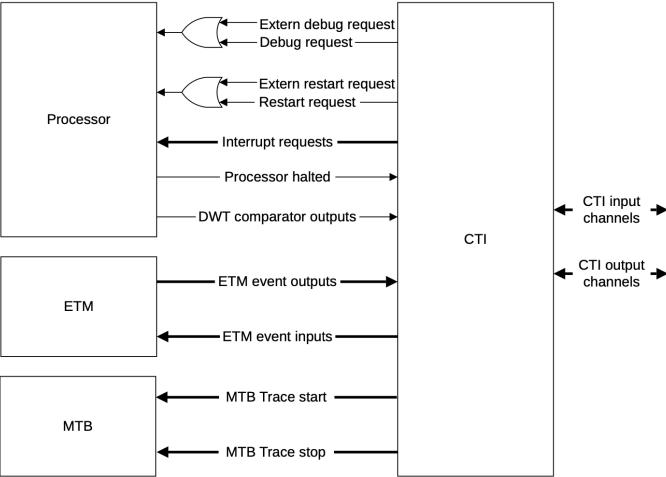
graph LR
    subgraph Processor
        direction TB
        P1[Extern debug request] --> CTI
        P2[Debug request] --> CTI
        P3[Extern restart request] --> CTI
        P4[Restart request] --> CTI
        P5[Interrupt requests] --> CTI
        P6[Processor halted] --> CTI
        P7[DWT comparator outputs] --> CTI
    end
    subgraph ETM
        direction TB
        E1[ETM event outputs] --> CTI
        E2[ETM event inputs] --> CTI
    end
    subgraph MTB
        direction TB
        M1[MTB Trace start] --> CTI
        M2[MTB Trace stop] --> CTI
    end
    subgraph CTI
        direction TB
        C1[CTI input channels]
        C2[CTI output channels]
endThe following table shows how the CTI trigger inputs are connected to the Cortex-M33 processor:
Table 118. Trigger signals to the CTI
| Signal | Description | Connection | Acknowledge, handshake |
|---|---|---|---|
| CTITRIGIN[7] | ETM to CTI | Pulsed | |
| CTITRIGIN[6] | ETM to CTI | Pulsed | |
| CTITRIGIN[5] | ETM Event Output 1 | ETM to CTI | Pulsed |
| CTITRIGIN[4] | ETM Event Output 0 or Comparator Output 3 | ETM/Processor to CTI | Pulsed |
| CTITRIGIN[3] | DWT Comparator Output 2 | Processor to CTI | Pulsed |
| CTITRIGIN[2] | DWT Comparator Output 1 | Processor to CTI | Pulsed |
| CTITRIGIN[1] | DWT Comparator Output 0 | Processor to CTI | Pulsed |
| CTITRIGIN[0] | Processor Halted | Processor to CTI | Pulsed |
The following table shows how the CTI trigger outputs are connected to the processor and ETM:
Table 119. Trigger signals from the CTI
| Signal | Description | Connection | Acknowledge, handshake |
|---|---|---|---|
| CTITRIGOUT[7] | ETM Event Input 3 | CTI to ETM | Pulsed |
| CTITRIGOUT[6] | ETM Event Input 2 | CTI to ETM | Pulsed |
| CTITRIGOUT[5] | ETM Event Input 1 or MTB Trace stop | CTI to ETM or MTB | Pulsed |
| CTITRIGOUT[4] | ETM Event Input 1 or MTB Trace start | CTI to ETM or MTB | Pulsed |
| CTITRIGOUT[3] | Interrupt request 1 | CTI to system | Acknowledged by writing to the CTIINTACK register in ISR |
| CTITRIGOUT[2] | Interrupt request 0 | CTI to system | Acknowledged by writing to the CTIINTACK register in ISR |
| CTITRIGOUT[1] | Processor Restart | CTI to Processor | Processor Restarted |
| Signal | Description | Connection | Acknowledge, handshake |
|---|---|---|---|
| CTITRIGOUT[0] | Processor debug request | CTI to Processor | Acknowledged by the debugger writing to the CTIINTACK register |
After the processor is halted using CTI Trigger Output 0, the Processor Debug Request signal remains asserted. The debugger must write to CTIINTACK to clear the halting request before restarting the processor.
After asserting an interrupt using the CTI Trigger Output 1 or 2, the Interrupt Service Routine (ISR) must clear the interrupt request by writing to the CTI Interrupt Acknowledge, CTIINTACK .
Interrupt requests from the CTI to the system are only asserted when invasive debug is enabled in the processor.
3.7.4.12.1. CTI programmers model
The following table shows the CTI programmable registers, with address offset, type, and reset value for each register. See the Arm CoreSight™ SoC-400 Technical Reference Manual for register descriptions.
Table 120. Cortex-M33
CTI register summary
| Address offset | Name | Type | Reset value | Description |
|---|---|---|---|---|
| 0xE0042000 | CTICONTROL | RW | 0x00000000 | CTI Control Register |
| 0xE0042010 | CTIINTACK | WO | UNKNOWN | CTI Interrupt Acknowledge Register |
| 0xE0042014 | CTIAPPSET | RW | 0x00000000 | CTI Application Trigger Set Register |
| 0xE0042018 | CTIAPPCLEAR | RW | 0x00000000 | CTI Application Trigger Clear Register |
| 0xE004201C | CTIAPPULSE | WO | UNKNOWN | CTI Application Pulse Register |
| 0xE0042020-0xE004203C | CTIINEN[7:0] | RW | 0x00000000 | CTI Trigger to Channel Enable Registers |
| 0xE00420A0-0xE00420BC | CTIOUTEN[7:0] | RW | 0x00000000 | CTI Channel to Trigger Enable Registers |
| 0xE0042130 | CTITRIGINSTATUS | RO | 0x00000000 | CTI Trigger In Status Register |
| 0xE0042134 | CTITRIGOUTSTATUS | RO | 0x00000000 | CTI Trigger Out Status Register |
| 0xE0042138 | CTICHINSTATUS | RO | 0x00000000 | CTI Channel In Status Register |
| 0xE0042140 | CTIGATE | RW | 0x0000000F | Enable CTI Channel Gate Register |
| 0xE0042144 | ASICCTL | RW | 0x00000000 | External Multiplexer Control Register |
| 0xE0042EE4 | ITCHOUT | WO | UNKNOWN | Integration Test Channel Output Register |
| 0xE0042EE8 | ITTRIGOUT | WO | UNKNOWN | Integration Test Trigger Output Register |
| 0xE0042EF4 | ITCHIN | RO | 0x00000000 | Integration Test Channel Input Register |
| 0xE0042F00 | ITCTRL | RW | 0x00000000 | Integration Mode Control Register |
| 0xE0042FC8 | DEVID | RO | 0x00040800 | Device Configuration Register |
| 0xE0042FBC | DEVARCH | RO | 0x47701A14 | Device Architecture Register |
| Address offset | Name | Type | Reset value | Description |
|---|---|---|---|---|
| 0xE0042FCC | DEVTYPE | RO | 0x00000014 | Device Type Identifier Register |
| 0xE0042FD0 | PIDR4 | RO | 0x00000004 | Peripheral ID4 Register |
| 0xE0042FD4 | PIDR5 | RO | 0x00000000 | Peripheral ID5 Register |
| 0xE0042FD8 | PIDR6 | RO | 0x00000000 | Peripheral ID6 Register |
| 0xE0042FDC | PIDR7 | RO | 0x00000000 | Peripheral ID7 Register |
| 0xE0042FE0 | PIDR0 | RO | 0x00000021 | Peripheral ID0 Register |
| 0xE0042FE4 | PIDR1 | RO | 0x000000BD | Peripheral ID1 Register |
| 0xE0042FE8 | PIDR2 | RO | 0x0000000B | Peripheral ID2 Register |
| 0xE0042FEC | PIDR3 | RO | 0x00000001 | Peripheral ID3 Register |
| 0xE0042FF0 | CIDR0 | RO | 0x0000000D | Component ID0 Register |
| 0xE0042FF4 | CIDR1 | RO | 0x00000090 | Component ID1 Register |
| 0xE0042FF8 | CIDR2 | RO | 0x00000005 | Component ID2 Register |
| 0xE0042FFC | CIDR3 | RO | 0x000000B1 | Component ID3 Register |
3.7.5. List of registers
The Arm Cortex-M33 registers start at a base address of 0xe0000000, defined as
PPB_BASE
in the SDK.
Table 121. List of M33 registers
| Offset | Name | Info |
|---|---|---|
| 0x00000 | ITM_STIM0 | ITM Stimulus Port Register 0 |
| 0x00004 | ITM_STIM1 | ITM Stimulus Port Register 1 |
| 0x00008 | ITM_STIM2 | ITM Stimulus Port Register 2 |
| 0x0000c | ITM_STIM3 | ITM Stimulus Port Register 3 |
| 0x00010 | ITM_STIM4 | ITM Stimulus Port Register 4 |
| 0x00014 | ITM_STIM5 | ITM Stimulus Port Register 5 |
| 0x00018 | ITM_STIM6 | ITM Stimulus Port Register 6 |
| 0x0001c | ITM_STIM7 | ITM Stimulus Port Register 7 |
| 0x00020 | ITM_STIM8 | ITM Stimulus Port Register 8 |
| 0x00024 | ITM_STIM9 | ITM Stimulus Port Register 9 |
| 0x00028 | ITM_STIM10 | ITM Stimulus Port Register 10 |
| 0x0002c | ITM_STIM11 | ITM Stimulus Port Register 11 |
| 0x00030 | ITM_STIM12 | ITM Stimulus Port Register 12 |
| 0x00034 | ITM_STIM13 | ITM Stimulus Port Register 13 |
| 0x00038 | ITM_STIM14 | ITM Stimulus Port Register 14 |
| 0x0003c | ITM_STIM15 | ITM Stimulus Port Register 15 |
| 0x00040 | ITM_STIM16 | ITM Stimulus Port Register 16 |
| 0x00044 | ITM_STIM17 | ITM Stimulus Port Register 17 |
| Offset | Name | Info |
|---|---|---|
| 0x00048 | ITM_STIM18 | ITM Stimulus Port Register 18 |
| 0x0004c | ITM_STIM19 | ITM Stimulus Port Register 19 |
| 0x00050 | ITM_STIM20 | ITM Stimulus Port Register 20 |
| 0x00054 | ITM_STIM21 | ITM Stimulus Port Register 21 |
| 0x00058 | ITM_STIM22 | ITM Stimulus Port Register 22 |
| 0x0005c | ITM_STIM23 | ITM Stimulus Port Register 23 |
| 0x00060 | ITM_STIM24 | ITM Stimulus Port Register 24 |
| 0x00064 | ITM_STIM25 | ITM Stimulus Port Register 25 |
| 0x00068 | ITM_STIM26 | ITM Stimulus Port Register 26 |
| 0x0006c | ITM_STIM27 | ITM Stimulus Port Register 27 |
| 0x00070 | ITM_STIM28 | ITM Stimulus Port Register 28 |
| 0x00074 | ITM_STIM29 | ITM Stimulus Port Register 29 |
| 0x00078 | ITM_STIM30 | ITM Stimulus Port Register 30 |
| 0x0007c | ITM_STIM31 | ITM Stimulus Port Register 31 |
| 0x00e00 | ITM_TER0 | Provide an individual enable bit for each ITM_STIM register |
| 0x00e40 | ITM_TPR | Controls which stimulus ports can be accessed by unprivileged code |
| 0x00e80 | ITM_TCR | Configures and controls transfers through the ITM interface |
| 0x00ef0 | INT_ATREADY | Integration Mode: Read ATB Ready |
| 0x00ef8 | INT_ATVALID | Integration Mode: Write ATB Valid |
| 0x00f00 | ITM_ITCTRL | Integration Mode Control Register |
| 0x00fbc | ITM_DEVARCH | Provides CoreSight discovery information for the ITM |
| 0x00fcc | ITM_DEVTYPE | Provides CoreSight discovery information for the ITM |
| 0x00fd0 | ITM_PIDR4 | Provides CoreSight discovery information for the ITM |
| 0x00fd4 | ITM_PIDR5 | Provides CoreSight discovery information for the ITM |
| 0x00fd8 | ITM_PIDR6 | Provides CoreSight discovery information for the ITM |
| 0x00fdc | ITM_PIDR7 | Provides CoreSight discovery information for the ITM |
| 0x00fe0 | ITM_PIDR0 | Provides CoreSight discovery information for the ITM |
| 0x00fe4 | ITM_PIDR1 | Provides CoreSight discovery information for the ITM |
| 0x00fe8 | ITM_PIDR2 | Provides CoreSight discovery information for the ITM |
| 0x00fec | ITM_PIDR3 | Provides CoreSight discovery information for the ITM |
| 0x00ff0 | ITM_CIDR0 | Provides CoreSight discovery information for the ITM |
| 0x00ff4 | ITM_CIDR1 | Provides CoreSight discovery information for the ITM |
| 0x00ff8 | ITM_CIDR2 | Provides CoreSight discovery information for the ITM |
| 0x00ffc | ITM_CIDR3 | Provides CoreSight discovery information for the ITM |
| Offset | Name | Info |
|---|---|---|
| 0x01000 | DWT_CTRL | Provides configuration and status information for the DWT unit, and used to control features of the unit |
| 0x01004 | DWT_CYCCNT | Shows or sets the value of the processor cycle counter, CYCCNT |
| 0x0100c | DWT_EXCCNT | Counts the total cycles spent in exception processing |
| 0x01014 | DWT_LSUCNT | Increments on the additional cycles required to execute all load or store instructions |
| 0x01018 | DWT_FOLDCNT | Increments on the additional cycles required to execute all load or store instructions |
| 0x01020 | DWT_COMP0 | Provides a reference value for use by watchpoint comparator 0 |
| 0x01028 | DWT_FUNCTION0 | Controls the operation of watchpoint comparator 0 |
| 0x01030 | DWT_COMP1 | Provides a reference value for use by watchpoint comparator 1 |
| 0x01038 | DWT_FUNCTION1 | Controls the operation of watchpoint comparator 1 |
| 0x01040 | DWT_COMP2 | Provides a reference value for use by watchpoint comparator 2 |
| 0x01048 | DWT_FUNCTION2 | Controls the operation of watchpoint comparator 2 |
| 0x01050 | DWT_COMP3 | Provides a reference value for use by watchpoint comparator 3 |
| 0x01058 | DWT_FUNCTION3 | Controls the operation of watchpoint comparator 3 |
| 0x01fbc | DWT_DEVARCH | Provides CoreSight discovery information for the DWT |
| 0x01fcc | DWT_DEVTYPE | Provides CoreSight discovery information for the DWT |
| 0x01fd0 | DWT_PIDR4 | Provides CoreSight discovery information for the DWT |
| 0x01fd4 | DWT_PIDR5 | Provides CoreSight discovery information for the DWT |
| 0x01fd8 | DWT_PIDR6 | Provides CoreSight discovery information for the DWT |
| 0x01fdc | DWT_PIDR7 | Provides CoreSight discovery information for the DWT |
| 0x01fe0 | DWT_PIDR0 | Provides CoreSight discovery information for the DWT |
| 0x01fe4 | DWT_PIDR1 | Provides CoreSight discovery information for the DWT |
| 0x01fe8 | DWT_PIDR2 | Provides CoreSight discovery information for the DWT |
| 0x01fec | DWT_PIDR3 | Provides CoreSight discovery information for the DWT |
| 0x01ff0 | DWT_CIDR0 | Provides CoreSight discovery information for the DWT |
| 0x01ff4 | DWT_CIDR1 | Provides CoreSight discovery information for the DWT |
| 0x01ff8 | DWT_CIDR2 | Provides CoreSight discovery information for the DWT |
| 0x01ffc | DWT_CIDR3 | Provides CoreSight discovery information for the DWT |
| 0x02000 | FP_CTRL | Provides FPB implementation information, and the global enable for the FPB unit |
| 0x02004 | FP_REMAP | Indicates whether the implementation supports Flash Patch remap and, if it does, holds the target address for remap |
| 0x02008 | FP_COMP0 | Holds an address for comparison. The effect of the match depends on the configuration of the FPB and whether the comparator is an instruction address comparator or a literal address comparator |
| Offset | Name | Info |
|---|---|---|
| 0x0200c | FP_COMP1 | Holds an address for comparison. The effect of the match depends on the configuration of the FPB and whether the comparator is an instruction address comparator or a literal address comparator |
| 0x02010 | FP_COMP2 | Holds an address for comparison. The effect of the match depends on the configuration of the FPB and whether the comparator is an instruction address comparator or a literal address comparator |
| 0x02014 | FP_COMP3 | Holds an address for comparison. The effect of the match depends on the configuration of the FPB and whether the comparator is an instruction address comparator or a literal address comparator |
| 0x02018 | FP_COMP4 | Holds an address for comparison. The effect of the match depends on the configuration of the FPB and whether the comparator is an instruction address comparator or a literal address comparator |
| 0x0201c | FP_COMP5 | Holds an address for comparison. The effect of the match depends on the configuration of the FPB and whether the comparator is an instruction address comparator or a literal address comparator |
| 0x02020 | FP_COMP6 | Holds an address for comparison. The effect of the match depends on the configuration of the FPB and whether the comparator is an instruction address comparator or a literal address comparator |
| 0x02024 | FP_COMP7 | Holds an address for comparison. The effect of the match depends on the configuration of the FPB and whether the comparator is an instruction address comparator or a literal address comparator |
| 0x02fbc | FP_DEVARCH | Provides CoreSight discovery information for the FPB |
| 0x02fcc | FP_DEVTYPE | Provides CoreSight discovery information for the FPB |
| 0x02fd0 | FP_PIDR4 | Provides CoreSight discovery information for the FP |
| 0x02fd4 | FP_PIDR5 | Provides CoreSight discovery information for the FP |
| 0x02fd8 | FP_PIDR6 | Provides CoreSight discovery information for the FP |
| 0x02fdc | FP_PIDR7 | Provides CoreSight discovery information for the FP |
| 0x02fe0 | FP_PIDR0 | Provides CoreSight discovery information for the FP |
| 0x02fe4 | FP_PIDR1 | Provides CoreSight discovery information for the FP |
| 0x02fe8 | FP_PIDR2 | Provides CoreSight discovery information for the FP |
| 0x02fec | FP_PIDR3 | Provides CoreSight discovery information for the FP |
| 0x02ff0 | FP_CIDR0 | Provides CoreSight discovery information for the FP |
| 0x02ff4 | FP_CIDR1 | Provides CoreSight discovery information for the FP |
| 0x02ff8 | FP_CIDR2 | Provides CoreSight discovery information for the FP |
| 0x02ffc | FP_CIDR3 | Provides CoreSight discovery information for the FP |
| 0x0e004 | ICTR | Provides information about the interrupt controller |
| Offset | Name | Info |
|---|---|---|
| 0x0e008 | ACTLR | Provides IMPLEMENTATION DEFINED configuration and control options |
| 0x0e010 | SYST_CSR | SysTick Control and Status Register |
| 0x0e014 | SYST_RVR | SysTick Reload Value Register |
| 0x0e018 | SYST_CVR | SysTick Current Value Register |
| 0x0e01c | SYST_CALIB | SysTick Calibration Value Register |
| 0x0e100 | NVIC_ISER0 | Enables or reads the enabled state of each group of 32 interrupts |
| 0x0e104 | NVIC_ISER1 | Enables or reads the enabled state of each group of 32 interrupts |
| 0x0e180 | NVIC_ICER0 | Clears or reads the enabled state of each group of 32 interrupts |
| 0x0e184 | NVIC_ICER1 | Clears or reads the enabled state of each group of 32 interrupts |
| 0x0e200 | NVIC_ISPR0 | Enables or reads the pending state of each group of 32 interrupts |
| 0x0e204 | NVIC_ISPR1 | Enables or reads the pending state of each group of 32 interrupts |
| 0x0e280 | NVIC_ICPR0 | Clears or reads the pending state of each group of 32 interrupts |
| 0x0e284 | NVIC_ICPR1 | Clears or reads the pending state of each group of 32 interrupts |
| 0x0e300 | NVIC_IABR0 | For each group of 32 interrupts, shows the active state of each interrupt |
| 0x0e304 | NVIC_IABR1 | For each group of 32 interrupts, shows the active state of each interrupt |
| 0x0e380 | NVIC_ITNS0 | For each group of 32 interrupts, determines whether each interrupt targets Non-secure or Secure state |
| 0x0e384 | NVIC_ITNS1 | For each group of 32 interrupts, determines whether each interrupt targets Non-secure or Secure state |
| 0x0e400 | NVIC_IPR0 | Sets or reads interrupt priorities |
| 0x0e404 | NVIC_IPR1 | Sets or reads interrupt priorities |
| 0x0e408 | NVIC_IPR2 | Sets or reads interrupt priorities |
| 0x0e40c | NVIC_IPR3 | Sets or reads interrupt priorities |
| 0x0e410 | NVIC_IPR4 | Sets or reads interrupt priorities |
| 0x0e414 | NVIC_IPR5 | Sets or reads interrupt priorities |
| 0x0e418 | NVIC_IPR6 | Sets or reads interrupt priorities |
| 0x0e41c | NVIC_IPR7 | Sets or reads interrupt priorities |
| 0x0e420 | NVIC_IPR8 | Sets or reads interrupt priorities |
| 0x0e424 | NVIC_IPR9 | Sets or reads interrupt priorities |
| 0x0e428 | NVIC_IPR10 | Sets or reads interrupt priorities |
| 0x0e42c | NVIC_IPR11 | Sets or reads interrupt priorities |
| 0x0e430 | NVIC_IPR12 | Sets or reads interrupt priorities |
| 0x0e434 | NVIC_IPR13 | Sets or reads interrupt priorities |
| 0x0e438 | NVIC_IPR14 | Sets or reads interrupt priorities |
| Offset | Name | Info |
|---|---|---|
| 0x0e43c | NVIC_IPR15 | Sets or reads interrupt priorities |
| 0x0ed00 | CPUID | Provides identification information for the PE, including an implementer code for the device and a device ID number |
| 0x0ed04 | ICSR | Controls and provides status information for NMI, PendSV, SysTick and interrupts |
| 0x0ed08 | VTOR | Vector Table Offset Register |
| 0x0ed0c | AIRCR | Application Interrupt and Reset Control Register |
| 0x0ed10 | SCR | System Control Register |
| 0x0ed14 | CCR | Sets or returns configuration and control data |
| 0x0ed18 | SHPR1 | Sets or returns priority for system handlers 4 - 7 |
| 0x0ed1c | SHPR2 | Sets or returns priority for system handlers 8 - 11 |
| 0x0ed20 | SHPR3 | Sets or returns priority for system handlers 12 - 15 |
| 0x0ed24 | SHCSR | Provides access to the active and pending status of system exceptions |
| 0x0ed28 | CFSR | Contains the three Configurable Fault Status Registers. 31:16 UFSR: Provides information on UsageFault exceptions 15:8 BFSR: Provides information on BusFault exceptions 7:0 MMFSR: Provides information on MemManage exceptions |
| 0x0ed2c | HFSR | Shows the cause of any HardFaults |
| 0x0ed30 | DFSR | Shows which debug event occurred |
| 0x0ed34 | MMFAR | Shows the address of the memory location that caused an MPU fault |
| 0x0ed38 | BFAR | Shows the address associated with a precise data access BusFault |
| 0x0ed40 | ID_PFR0 | Gives top-level information about the instruction set supported by the PE |
| 0x0ed44 | ID_PFR1 | Gives information about the programmers' model and Extensions support |
| 0x0ed48 | ID_DFR0 | Provides top level information about the debug system |
| 0x0ed4c | ID_AFR0 | Provides information about the IMPLEMENTATION DEFINED features of the PE |
| 0x0ed50 | ID_MMFR0 | Provides information about the implemented memory model and memory management support |
| 0x0ed54 | ID_MMFR1 | Provides information about the implemented memory model and memory management support |
| 0x0ed58 | ID_MMFR2 | Provides information about the implemented memory model and memory management support |
| 0x0ed5c | ID_MMFR3 | Provides information about the implemented memory model and memory management support |
| Offset | Name | Info |
|---|---|---|
| 0x0ed60 | ID_ISAR0 | Provides information about the instruction set implemented by the PE |
| 0x0ed64 | ID_ISAR1 | Provides information about the instruction set implemented by the PE |
| 0x0ed68 | ID_ISAR2 | Provides information about the instruction set implemented by the PE |
| 0x0ed6c | ID_ISAR3 | Provides information about the instruction set implemented by the PE |
| 0x0ed70 | ID_ISAR4 | Provides information about the instruction set implemented by the PE |
| 0x0ed74 | ID_ISAR5 | Provides information about the instruction set implemented by the PE |
| 0x0ed7c | CTR | Provides information about the architecture of the caches. CTR is RES0 if CLIDR is zero. |
| 0x0ed88 | CPACR | Specifies the access privileges for coprocessors and the FP Extension |
| 0x0ed8c | NSACR | Defines the Non-secure access permissions for both the FP Extension and coprocessors CP0 to CP7 |
| 0x0ed90 | MPU_TYPE | The MPU Type Register indicates how many regions the MPU `FTSSS supports |
| 0x0ed94 | MPU_CTRL | Enables the MPU and, when the MPU is enabled, controls whether the default memory map is enabled as a background region for privileged accesses, and whether the MPU is enabled for HardFaults, NMIs, and exception handlers when FAULTMASK is set to 1 |
| 0x0ed98 | MPU_RNR | Selects the region currently accessed by MPU_RBAR and MPU_RLAR |
| 0x0ed9c | MPU_RBAR | Provides indirect read and write access to the base address of the currently selected MPU region `FTSSS |
| 0x0eda0 | MPU_RLAR | Provides indirect read and write access to the limit address of the currently selected MPU region `FTSSS |
| 0x0eda4 | MPU_RBAR_A1 | Provides indirect read and write access to the base address of the MPU region selected by MPU_RNR[7:2]:(1[1:0]) `FTSSS |
| 0x0eda8 | MPU_RLAR_A1 | Provides indirect read and write access to the limit address of the currently selected MPU region selected by MPU_RNR[7:2]:(1[1:0]) `FTSSS |
| 0x0edac | MPU_RBAR_A2 | Provides indirect read and write access to the base address of the MPU region selected by MPU_RNR[7:2]:(2[1:0]) `FTSSS |
| 0x0edb0 | MPU_RLAR_A2 | Provides indirect read and write access to the limit address of the currently selected MPU region selected by MPU_RNR[7:2]:(2[1:0]) `FTSSS |
| 0x0edb4 | MPU_RBAR_A3 | Provides indirect read and write access to the base address of the MPU region selected by MPU_RNR[7:2]:(3[1:0]) `FTSSS |
| Offset | Name | Info |
|---|---|---|
| 0x0edb8 | MPU_RLAR_A3 | Provides indirect read and write access to the limit address of the currently selected MPU region selected by MPU_RNR[7:2]:(3[1:0]) `FTSSS |
| 0x0edc0 | MPU_MAIR0 | Along with MPU_MAIR1, provides the memory attribute encodings corresponding to the AttrIndex values |
| 0x0edc4 | MPU_MAIR1 | Along with MPU_MAIR0, provides the memory attribute encodings corresponding to the AttrIndex values |
| 0x0edd0 | SAU_CTRL | Allows enabling of the Security Attribution Unit |
| 0x0edd4 | SAU_TYPE | Indicates the number of regions implemented by the Security Attribution Unit |
| 0x0edd8 | SAU_RNR | Selects the region currently accessed by SAU_RBAR and SAU_RLAR |
| 0x0eddc | SAU_RBAR | Provides indirect read and write access to the base address of the currently selected SAU region |
| 0x0ede0 | SAU_RLAR | Provides indirect read and write access to the limit address of the currently selected SAU region |
| 0x0ede4 | SFSR | Provides information about any security related faults |
| 0x0ede8 | SFAR | Shows the address of the memory location that caused a Security violation |
| 0x0edf0 | DHCSR | Controls halting debug |
| 0x0edf4 | DCRSR | With the DCRDR, provides debug access to the general-purpose registers, special-purpose registers, and the FP extension registers. A write to the DCRSR specifies the register to transfer, whether the transfer is a read or write, and starts the transfer |
| 0x0edf8 | DCRDR | With the DCRSR, provides debug access to the general-purpose registers, special-purpose registers, and the FP Extension registers. If the Main Extension is implemented, it can also be used for message passing between an external debugger and a debug agent running on the PE |
| 0x0edfc | DEMCR | Manages vector catch behavior and DebugMonitor handling when debugging |
| 0x0ee08 | DSCSR | Provides control and status information for Secure debug |
| 0x0ef00 | STIR | Provides a mechanism for software to generate an interrupt |
| 0x0ef34 | FPCCR | Holds control data for the Floating-point extension |
| 0x0ef38 | FPCAR | Holds the location of the unpopulated floating-point register space allocated on an exception stack frame |
| 0x0ef3c | FPDSCR | Holds the default values for the floating-point status control data that the PE assigns to the FPSCR when it creates a new floating-point context |
| 0x0ef40 | MVFR0 | Describes the features provided by the Floating-point Extension |
| 0x0ef44 | MVFR1 | Describes the features provided by the Floating-point Extension |
| 0x0ef48 | MVFR2 | Describes the features provided by the Floating-point Extension |
| 0x0efbc | DDEVARCH | Provides CoreSight discovery information for the SCS |
| Offset | Name | Info |
|---|---|---|
| 0x0efcc | DDEVTYPE | Provides CoreSight discovery information for the SCS |
| 0x0efd0 | DPIDR4 | Provides CoreSight discovery information for the SCS |
| 0x0efd4 | DPIDR5 | Provides CoreSight discovery information for the SCS |
| 0x0efd8 | DPIDR6 | Provides CoreSight discovery information for the SCS |
| 0x0efdc | DPIDR7 | Provides CoreSight discovery information for the SCS |
| 0x0efe0 | DPIDR0 | Provides CoreSight discovery information for the SCS |
| 0x0efe4 | DPIDR1 | Provides CoreSight discovery information for the SCS |
| 0x0efe8 | DPIDR2 | Provides CoreSight discovery information for the SCS |
| 0x0efec | DPIDR3 | Provides CoreSight discovery information for the SCS |
| 0x0eff0 | DCIDR0 | Provides CoreSight discovery information for the SCS |
| 0x0eff4 | DCIDR1 | Provides CoreSight discovery information for the SCS |
| 0x0eff8 | DCIDR2 | Provides CoreSight discovery information for the SCS |
| 0x0effc | DCIDR3 | Provides CoreSight discovery information for the SCS |
| 0x41004 | TRCPRGCTLR | Programming Control Register |
| 0x4100c | TRCSTATR | The TRCSTATR indicates the ETM-Teal status |
| 0x41010 | TRCCONFIGR | The TRCCONFIGR sets the basic tracing options for the trace unit |
| 0x41020 | TRCEVENTCTL0R | The TRCEVENTCTL0R controls the tracing of events in the trace stream. The events also drive the ETM-Teal external outputs. |
| 0x41024 | TRCEVENTCTL1R | The TRCEVENTCTL1R controls how the events selected by TRCEVENTCTL0R behave |
| 0x4102c | TRCSTALLCTLR | The TRCSTALLCTLR enables ETM-Teal to stall the processor if the ETM-Teal FIFO goes over the programmed level to minimize risk of overflow |
| 0x41030 | TRCTSCTLR | The TRCTSCTLR controls the insertion of global timestamps into the trace stream. A timestamp is always inserted into the instruction trace stream |
| 0x41034 | TRCSYNCPR | The TRCSYNCPR specifies the period of trace synchronization of the trace streams. TRCSYNCPR defines a number of bytes of trace between requests for trace synchronization. This value is always a power of two |
| 0x41038 | TRCCCCTLR | The TRCCCCTLR sets the threshold value for instruction trace cycle counting. The threshold represents the minimum interval between cycle count trace packets |
| 0x41080 | TRCVICTLR | The TRCVICTLR controls instruction trace filtering |
| 0x41140 | TRCCNTRLDVR0 | The TRCCNTRLDVR defines the reload value for the reduced function counter |
| 0x41180 | TRCIDR8 | TRCIDR8 |
| 0x41184 | TRCIDR9 | TRCIDR9 |
| 0x41188 | TRCIDR10 | TRCIDR10 |
| Offset | Name | Info |
|---|---|---|
| 0x4118c | TRCIDR11 | TRCIDR11 |
| 0x41190 | TRCIDR12 | TRCIDR12 |
| 0x41194 | TRCIDR13 | TRCIDR13 |
| 0x411c0 | TRCIMSPEC | The TRCIMSPEC shows the presence of any IMPLEMENTATION SPECIFIC features, and enables any features that are provided |
| 0x411e0 | TRCIDR0 | TRCIDR0 |
| 0x411e4 | TRCIDR1 | TRCIDR1 |
| 0x411e8 | TRCIDR2 | TRCIDR2 |
| 0x411ec | TRCIDR3 | TRCIDR3 |
| 0x411f0 | TRCIDR4 | TRCIDR4 |
| 0x411f4 | TRCIDR5 | TRCIDR5 |
| 0x411f8 | TRCIDR6 | TRCIDR6 |
| 0x411fc | TRCIDR7 | TRCIDR7 |
| 0x41208 | TRCRSCTLR2 | The TRCRSCTLR controls the trace resources |
| 0x4120c | TRCRSCTLR3 | The TRCRSCTLR controls the trace resources |
| 0x412a0 | TRCSSCSR | Controls the corresponding single-shot comparator resource |
| 0x412c0 | TRCSSPCICR | Selects the PE comparator inputs for Single-shot control |
| 0x41310 | TRCPDCR | Requests the system to provide power to the trace unit |
| 0x41314 | TRCPDSR | Returns the following information about the trace unit: - OS Lock status. - Core power domain status. - Power interruption status |
| 0x41ee4 | TRCITATBIDR | Trace Intergration ATB Identification Register |
| 0x41ef4 | TRCITIATBINR | Trace Integration Instruction ATB In Register |
| 0x41efc | TRCITIATBOUTR | Trace Integration Instruction ATB Out Register |
| 0x41fa0 | TRCCLAIMSET | Claim Tag Set Register |
| 0x41fa4 | TRCCLAIMCLR | Claim Tag Clear Register |
| 0x41fb8 | TRCAUTHSTATUS | Returns the level of tracing that the trace unit can support |
| 0x41fbc | TRCDEVARCH | TRCDEVARCH |
| 0x41fc8 | TRCDEVID | TRCDEVID |
| 0x41fcc | TRCDEVTYPE | TRCDEVTYPE |
| 0x41fd0 | TRCPIDR4 | TRCPIDR4 |
| 0x41fd4 | TRCPIDR5 | TRCPIDR5 |
| 0x41fd8 | TRCPIDR6 | TRCPIDR6 |
| 0x41fdc | TRCPIDR7 | TRCPIDR7 |
| 0x41fe0 | TRCPIDR0 | TRCPIDR0 |
| 0x41fe4 | TRCPIDR1 | TRCPIDR1 |
| 0x41fe8 | TRCPIDR2 | TRCPIDR2 |
| Offset | Name | Info |
|---|---|---|
| 0x41fec | TRCPIDR3 | TRCPIDR3 |
| 0x41ff0 | TRCCIDR0 | TRCCIDR0 |
| 0x41ff4 | TRCCIDR1 | TRCCIDR1 |
| 0x41ff8 | TRCCIDR2 | TRCCIDR2 |
| 0x41ffc | TRCCIDR3 | TRCCIDR3 |
| 0x42000 | CTICONTROL | CTI Control Register |
| 0x42010 | CTIINTACK | CTI Interrupt Acknowledge Register |
| 0x42014 | CTIAPPSET | CTI Application Trigger Set Register |
| 0x42018 | CTIAPPCLEAR | CTI Application Trigger Clear Register |
| 0x4201c | CTIAPPULSE | CTI Application Pulse Register |
| 0x42020 | CTIINEN0 | CTI Trigger to Channel Enable Registers |
| 0x42024 | CTIINEN1 | CTI Trigger to Channel Enable Registers |
| 0x42028 | CTIINEN2 | CTI Trigger to Channel Enable Registers |
| 0x4202c | CTIINEN3 | CTI Trigger to Channel Enable Registers |
| 0x42030 | CTIINEN4 | CTI Trigger to Channel Enable Registers |
| 0x42034 | CTIINEN5 | CTI Trigger to Channel Enable Registers |
| 0x42038 | CTIINEN6 | CTI Trigger to Channel Enable Registers |
| 0x4203c | CTIINEN7 | CTI Trigger to Channel Enable Registers |
| 0x420a0 | CTIOUTEN0 | CTI Trigger to Channel Enable Registers |
| 0x420a4 | CTIOUTEN1 | CTI Trigger to Channel Enable Registers |
| 0x420a8 | CTIOUTEN2 | CTI Trigger to Channel Enable Registers |
| 0x420ac | CTIOUTEN3 | CTI Trigger to Channel Enable Registers |
| 0x420b0 | CTIOUTEN4 | CTI Trigger to Channel Enable Registers |
| 0x420b4 | CTIOUTEN5 | CTI Trigger to Channel Enable Registers |
| 0x420b8 | CTIOUTEN6 | CTI Trigger to Channel Enable Registers |
| 0x420bc | CTIOUTEN7 | CTI Trigger to Channel Enable Registers |
| 0x42130 | CTITRIGINSTATUS | CTI Trigger to Channel Enable Registers |
| 0x42134 | CTITRIGOUTSTATUS | CTI Trigger In Status Register |
| 0x42138 | CTICHINSTATUS | CTI Channel In Status Register |
| 0x42140 | CTIGATE | Enable CTI Channel Gate register |
| 0x42144 | ASICCTL | External Multiplexer Control register |
| 0x42ee4 | ITCHOUT | Integration Test Channel Output register |
| 0x42ee8 | ITTRIGOUT | Integration Test Trigger Output register |
| 0x42ef4 | ITCHIN | Integration Test Channel Input register |
| 0x42f00 | ITCTRL | Integration Mode Control register |
| 0x42fbc | DEVARCH | Device Architecture register |
| Offset | Name | Info |
|---|---|---|
| 0x42fc8 | DEVID | Device Configuration register |
| 0x42fcc | DEVTYPE | Device Type Identifier register |
| 0x42fd0 | PIDR4 | CoreSight Periperal ID4 |
| 0x42fd4 | PIDR5 | CoreSight Periperal ID5 |
| 0x42fd8 | PIDR6 | CoreSight Periperal ID6 |
| 0x42fdc | PIDR7 | CoreSight Periperal ID7 |
| 0x42fe0 | PIDR0 | CoreSight Periperal ID0 |
| 0x42fe4 | PIDR1 | CoreSight Periperal ID1 |
| 0x42fe8 | PIDR2 | CoreSight Periperal ID2 |
| 0x42fec | PIDR3 | CoreSight Periperal ID3 |
| 0x42ff0 | CIDR0 | CoreSight Component ID0 |
| 0x42ff4 | CIDR1 | CoreSight Component ID1 |
| 0x42ff8 | CIDR2 | CoreSight Component ID2 |
| 0x42ffc | CIDR3 | CoreSight Component ID3 |
M33: ITM_STIM0, ITM_STIM1, ..., ITM_STIM30, ITM_STIM31 Registers
Offsets: 0x00000, 0x00004, ..., 0x00078, 0x0007c
Description
Provides the interface for generating Instrumentation packets
Table 122.
ITM_STIM0,
ITM_STIM1, ...,
ITM_STIM30,
ITM_STIM31 Registers
| Bits | Description | Type | Reset |
|---|---|---|---|
| 31:0 | STIMULUS: Data to write to the Stimulus Port FIFO, for forwarding as an Instrumentation packet. The size of write access determines the type of Instrumentation packet generated. | RW | 0x00000000 |
M33: ITM_TERO Register
Offset: 0x00e00
Description
Provide an individual enable bit for each ITM_STIM register
Table 123. ITM_TERO
Register
| Bits | Description | Type | Reset |
|---|---|---|---|
| 31:0 | STIMENA: For STIMENA[m] in ITM_TER*n, controls whether ITM_STIM(32*n + m) is enabled | RW | 0x00000000 |
M33: ITM_TPR Register
Offset: 0x00e40
Description
Controls which stimulus ports can be accessed by unprivileged code
Table 124. ITM_TPR
Register
| Bits | Description | Type | Reset |
|---|---|---|---|
| 31:4 | Reserved. | - | - |
| Bits 31:0 Bits 31:0 Bits 31:28 | column_2 | Description Description Input value for GPIO0…31. Description QSPI_SD : Input value on QSPI SD0 (MOSI), SD1 (MISO), SD2 and SD3 pins | Type RO Type RO Type RO | Reset - Reset 0x00000000 Reset 0x0 |
|---|---|---|---|---|
| 31:24 | Reserved. | - | - | |
| 23 | BUSY | : Indicates whether the ITM is currently processing events | RO | 0x0 |
| 22:16 | TRACEBUSID | : Identifier for multi-source trace stream formatting. If multi- source trace is in use, the debugger must write a unique non-zero trace ID | RW | 0x00 |
| 15:12 | Reserved. | - | - | |
| 11:10 | GTSFREQ | : Defines how often the ITM generates a global timestamp, based on the global timestamp clock frequency, or disables generation of global | RW | 0x0 |
| 9:8 | TSPRESCALE | timestamps : Local timestamp prescaler, used with the trace packet | RW | 0x0 |
| 7:6 | Reserved. | - | - | |
| 5 | STALLENA | : Stall the PE to guarantee delivery of Data Trace packets. | RW | 0x0 |
| 4 | SWOENA | : Enables asynchronous clocking of the timestamp counter | RW | 0x0 |
| 3 | TXENA | : Enables forwarding of hardware event packet from the DWT unit to | RW | 0x0 |
| 2 | SYNCENA | the ITM for output to the TPIU : Enables Synchronization packet transmission for a synchronous | RW | 0x0 |
| 1 | TPIU TSENA | : Enables Local timestamp generation | RW | 0x0 |
| 0 | ITMENA | : Enables the ITM | RW | 0x0 |
| Bits | Description | Type | Reset | |
| Register 31:2 | Reserved. | - | - | |
| 1 | AFVALID | : A read of this bit returns the value of AFVALID | RO | 0x0 |
| 0 | ATREADY | : A read of this bit returns the value of ATREADY | RO | 0x0 |
M33: ITM_TCR Register
Offset: 0x00e80
Description
Configures and controls transfers through the ITM interface
Table 125. ITM_TCR Register
M33: INT_ATREADY Register
Offset: 0x00ef0
Description
Integration Mode: Read ATB Ready
Table 126. INT_ATREADY Register
M33: INT_ATVALID Register
Offset: 0x00ef8
DescriptionIntegration Mode: Write ATB Valid
Table 127.INT_ATVALID Register
| Bits 31:0 Bits 31:0 Bits 31:28 | column_2 | Description Description Input value for GPIO0…31. Description QSPI_SD : Input value on QSPI SD0 (MOSI), SD1 (MISO), SD2 and SD3 pins | Type RO Type RO Type RO | Reset - Reset 0x00000000 Reset 0x0 |
|---|---|---|---|---|
| 31:2 | Reserved. | - | - | |
| 1 | AFREADY | : A write to this bit gives the value of AFREADY | RW | 0x0 |
| 0 | ATREADY | : A write to this bit gives the value of ATVALID | RW | 0x0 |
| Table 128. Bits | Description | Type | Reset | |
| ITM_ITCTRL Register 31:1 | Reserved. | - | - | |
| 0 | IME : Integration mode enable bit - The possible values are: 0 - The trace unit is | RW | 0x0 | |
| Table 129. Bits | Description | Type | Reset | |
| ITM_DEVARCH Register 31:21 | ARCHITECT | : Defines the architect of the component. Bits [31:28] are the | RO | 0x23b |
| 20 | PRESENT | JEP106 ID code. : Defines that the DEVARCH register is present | RO | 0x1 |
| 19:16 | REVISION | : Defines the architecture revision of the component | RO | 0x0 |
| 15:12 | ARCHVER | : Defines the architecture version of the component | RO | 0x1 |
| 11:0 | ARCHPART | : Defines the architecture of the component | RO | 0xa01 |
| Table 130. Bits | Description | Type | Reset | |
| ITM_DEVTYPE Register 31:8 | Reserved. | - | - | |
| 7:4 | SUB : Component sub-type | RO | 0x4 | |
| 3:0 | MAJOR | : Component major type | RO | 0x3 |
Integration Mode Control Register
Table 128.ITM_ITCTRL Register M33: ITM_DEVARCH Register Offset: 0x00fbc Description
Provides CoreSight discovery information for the ITM
Table 129.ITM_DEVARCH Register M33: ITM_DEVTYPE Register Offset: 0x00fcc Description
Provides CoreSight discovery information for the ITM
Table 130.ITM_DEVTYPE Register M33: ITM_PIDR4 Register
Offset: 0x00fd0
Description
Provides CoreSight discovery information for the ITM
Table 131. ITM_PIDR4 Register
| Bits | Description | Type | Reset |
|---|---|---|---|
| 31:8 | Reserved. | - | - |
| 7:4 | SIZE: See CoreSight Architecture Specification | RO | 0x0 |
| 3:0 | DES_2: See CoreSight Architecture Specification | RO | 0x4 |
M33: ITM_PIDR5 Register
Offset: 0x00fd4
Description
Provides CoreSight discovery information for the ITM
Table 132. ITM_PIDR5 Register
| Bits | Description | Type | Reset |
|---|---|---|---|
| 31:0 | Reserved. | - | - |
M33: ITM_PIDR6 Register
Offset: 0x00fd8
Description
Provides CoreSight discovery information for the ITM
Table 133. ITM_PIDR6 Register
| Bits | Description | Type | Reset |
|---|---|---|---|
| 31:0 | Reserved. | - | - |
M33: ITM_PIDR7 Register
Offset: 0x00fdc
Description
Provides CoreSight discovery information for the ITM
Table 134. ITM_PIDR7 Register
| Bits | Description | Type | Reset |
|---|---|---|---|
| 31:0 | Reserved. | - | - |
M33: ITM_PIDR0 Register
Offset: 0x00fe0
Description
Provides CoreSight discovery information for the ITM
Table 135. ITM_PIDR0 Register
| Bits | Description | Type | Reset |
|---|---|---|---|
| 31:8 | Reserved. | - | - |
| 7:0 | PART_0 : See CoreSight Architecture Specification | RO | 0x21 |
M33: ITM_PIDR1 Register
Offset: 0x00fe4
Description
Provides CoreSight discovery information for the ITM
Table 136. ITM_PIDR1 Register
| Bits | Description | Type | Reset |
|---|---|---|---|
| 31:8 | Reserved. | - | - |
| 7:4 | DES_0 : See CoreSight Architecture Specification | RO | 0xb |
| 3:0 | PART_1 : See CoreSight Architecture Specification | RO | 0xd |
M33: ITM_PIDR2 Register
Offset: 0x00fe8
Description
Provides CoreSight discovery information for the ITM
Table 137. ITM_PIDR2 Register
| Bits | Description | Type | Reset |
|---|---|---|---|
| 31:8 | Reserved. | - | - |
| 7:4 | REVISION : See CoreSight Architecture Specification | RO | 0x0 |
| 3 | JEDEC : See CoreSight Architecture Specification | RO | 0x1 |
| 2:0 | DES_1 : See CoreSight Architecture Specification | RO | 0x3 |
M33: ITM_PIDR3 Register
Offset: 0x00fec
Description
Provides CoreSight discovery information for the ITM
Table 138. ITM_PIDR3 Register
| Bits | Description | Type | Reset |
|---|---|---|---|
| 31:8 | Reserved. | - | - |
| 7:4 | REVAND : See CoreSight Architecture Specification | RO | 0x0 |
| 3:0 | CMOD : See CoreSight Architecture Specification | RO | 0x0 |
M33: ITM_CIDR0 Register
Offset: 0x00ff0
Description
Provides CoreSight discovery information for the ITM
Table 139. ITM_CIDR0 Register
| Bits | Description | Type | Reset |
|---|---|---|---|
| 31:8 | Reserved. | - | - |
| 7:0 | PRMBL_0 : See CoreSight Architecture Specification | RO | 0x0d |
M33: ITM_CIDR1 Register
Offset: 0x00ff4
Description
Provides CoreSight discovery information for the ITM
Table 140. ITM_CIDR1 Register
| Bits | Description | Type | Reset |
|---|---|---|---|
| 31:8 | Reserved. | - | - |
| 7:4 | CLASS : See CoreSight Architecture Specification | RO | 0x9 |
| 3:0 | PRMBL_1 : See CoreSight Architecture Specification | RO | 0x0 |
M33: ITM_CIDR2 Register
Offset: 0x00ff8
Description
Provides CoreSight discovery information for the ITM
Table 141. ITM_CIDR2 Register
| Bits | Description | Type | Reset |
|---|---|---|---|
| 31:8 | Reserved. | - | - |
| 7:0 | PRMBL_2 : See CoreSight Architecture Specification | RO | 0x05 |
M33: ITM_CIDR3 Register
Offset: 0x00ffc
Description
Provides CoreSight discovery information for the ITM
Table 142. ITM_CIDR3 Register
| Bits | Description | Type | Reset |
|---|---|---|---|
| 31:8 | Reserved. | - | - |
| 7:0 | PRMBL_3 : See CoreSight Architecture Specification | RO | 0xb1 |
M33: DWT_CTRL Register
Offset: 0x01000
Description
Provides configuration and status information for the DWT unit, and used to control features of the unit
Table 143. DWT_CTRL Register
| Bits | Description | Type | Reset |
|---|---|---|---|
| 31:28 | NUMCOMP : Number of DWT comparators implemented | RO | 0x7 |
| 27 | NOTRCPKT : Indicates whether the implementation does not support trace | RO | 0x0 |
| 26 | NOEXTTRIG : Reserved, RAZ | RO | 0x0 |
| 25 | NOCYCCNT : Indicates whether the implementation does not include a cycle counter | RO | 0x1 |
| Bits 14:10 9:5 4:0 Bits | Description SHIFT Description | MASK_MSB : The most-significant bit allowed to pass by the mask (inclusive) MASK_LSB : The least-significant bit allowed to pass by the mask (inclusive) : Right-rotate applied to accumulator before masking. By appropriately | Type RW RW RW Type | Reset 0x00 0x00 0x00 Reset |
|---|---|---|---|---|
| 19 | SLEEPEVTENA | : Enable DWT_SLEEPCNT counter | RW | 0x0 |
| 18 | EXCEVTENA | : Enables DWT_EXCCNT counter | RW | 0x1 |
| 17 | CPIEVTENA | : Enables DWT_CPICNT counter | RW | 0x0 |
| 16 | EXTTRCENA | : Enables generation of Exception Trace packets | RW | 0x0 |
| 15:13 | Reserved. | - | - | |
| 12 | PCSAMPLENA | : Enables use of POSTCNT counter as a timer for Periodic PC | RW | 0x1 |
| 11:10 | SYNCTAP | Sample packet generation : Selects the position of the synchronization packet counter tap on | RW | 0x2 |
| 9 | CYCTAP | the CYCCNT counter. This determines the Synchronization packet rate : Selects the position of the POSTCNT tap on the CYCCNT counter | RW | 0x0 |
| 8:5 | POSTINIT | : Initial value for the POSTCNT counter | RW | 0x1 |
| 4:1 | POSTPRESET | : Reload value for the POSTCNT counter | RW | 0x2 |
| 0 | CYCCNTENA | : Enables CYCCNT | RW | 0x0 |
| Table 144. Bits | Description | Type | Reset | |
| DWT_CYCCNT Register 31:0 | CYCCNT | : Increments one on each processor clock cycle when DWT_CTRL.CYCCNTENA == 1 and DEMCR.TRCENA == 1. On overflow, | RW | 0x00000000 |
| Table 145. Bits | Description | Type | Reset | |
| DWT_EXCCNT Register 31:8 | Reserved. | - | - |
M33: DWT_CYCCNT Register
Offset: 0x01004
Description
Shows or sets the value of the processor cycle counter, CYCCNT
Table 144.
DWT_CYCCNT
Register
M33: DWT_EXCCNT Register
Offset: 0x0100c
Description
Counts the total cycles spent in exception processing
Table 145.
DWT_EXCCNT
Register
| Bits | Description | Type | Reset |
|---|---|---|---|
| 7:0 | EXCCNT : Counts one on each cycle when all of the following are true: - DWT_CTRL.EXCEVTENA == 1 and DEMCR.TRCENA == 1. - No instruction is executed, see DWT_CPICNT. - An exception-entry or exception-exit related operation is in progress. - Either SecureNoninvasiveDebugAllowed() == TRUE, or NS-Req for the operation is set to Non-secure and NoninvasiveDebugAllowed() == TRUE. | RW | 0x00 |
M33: DWT_LSUCNT Register
Offset: 0x01014
Description
Increments on the additional cycles required to execute all load or store instructions
Table 146.
DWT_LSUCNT Register
| Bits | Description | Type | Reset |
|---|---|---|---|
| 31:8 | Reserved. | - | - |
| 7:0 | LSUCNT : Counts one on each cycle when all of the following are true: - DWT_CTRL.LSUEVTENA == 1 and DEMCR.TRCENA == 1. - No instruction is executed, see DWT_CPICNT. - No exception-entry or exception-exit operation is in progress, see DWT_EXCCNT. - A load-store operation is in progress. - Either SecureNoninvasiveDebugAllowed() == TRUE, or NS-Req for the operation is set to Non-secure and NoninvasiveDebugAllowed() == TRUE. | RW | 0x00 |
M33: DWT_FOLDCNT Register
Offset: 0x01018
Description
Increments on the additional cycles required to execute all load or store instructions
Table 147.
DWT_FOLDCNT Register
| Bits | Description | Type | Reset |
|---|---|---|---|
| 31:8 | Reserved. | - | - |
| 7:0 | FOLDCNT : Counts on each cycle when all of the following are true: - DWT_CTRL.FOLDEVTEA == 1 and DEMCR.TRCENA == 1. - At least two instructions are executed, see DWT_CPICNT. - Either SecureNoninvasiveDebugAllowed() == TRUE, or the PE is in Non-secure state and NoninvasiveDebugAllowed() == TRUE. The counter is incremented by the number of instructions executed, minus one | RW | 0x00 |
M33: DWT_COMP0 Register
Offset: 0x01020
Table 148.
DWT_COMP0 Register
| Bits | Description | Type | Reset |
|---|---|---|---|
| 31:0 | Provides a reference value for use by watchpoint comparator 0 | RW | 0x00000000 |
M33: DWT_FUNCTION0 Register
Offset: 0x01028
Description
Controls the operation of watchpoint comparator 0
Table 149.
DWT_FUNCTION0
Register
| Bits | Description | Type | Reset |
|---|---|---|---|
| 31:27 | ID : Identifies the capabilities for MATCH for comparator *n | RO | 0x0b |
| 26:25 | Reserved. | - | - |
| 24 | MATCHED : Set to 1 when the comparator matches | RO | 0x0 |
| 23:12 | Reserved. | - | - |
| 11:10 | DATAVSIZE : Defines the size of the object being watched for by Data Value and Data Address comparators | RW | 0x0 |
| 9:6 | Reserved. | - | - |
| 5:4 | ACTION : Defines the action on a match. This field is ignored and the comparator generates no actions if it is disabled by MATCH | RW | 0x0 |
| 3:0 | MATCH : Controls the type of match generated by this comparator | RW | 0x0 |
M33: DWT_COMP1 Register
Offset: 0x01030
Table 150.
DWT_COMP1 Register
| Bits | Description | Type | Reset |
|---|---|---|---|
| 31:0 | Provides a reference value for use by watchpoint comparator 1 | RW | 0x00000000 |
M33: DWT_FUNCTION1 Register
Offset: 0x01038
Description
Controls the operation of watchpoint comparator 1
Table 151.
DWT_FUNCTION1
Register
| Bits | Description | Type | Reset |
|---|---|---|---|
| 31:27 | ID : Identifies the capabilities for MATCH for comparator *n | RO | 0x11 |
| 26:25 | Reserved. | - | - |
| 24 | MATCHED : Set to 1 when the comparator matches | RO | 0x1 |
| 23:12 | Reserved. | - | - |
| 11:10 | DATAVSIZE : Defines the size of the object being watched for by Data Value and Data Address comparators | RW | 0x2 |
| 9:6 | Reserved. | - | - |
| 5:4 | ACTION : Defines the action on a match. This field is ignored and the comparator generates no actions if it is disabled by MATCH | RW | 0x2 |
| 3:0 | MATCH : Controls the type of match generated by this comparator | RW | 0x8 |
M33: DWT_COMP2 Register
Offset: 0x01040
Table 152.
DWT_COMP2 Register
| Bits | Description | Type | Reset |
|---|---|---|---|
| 31:0 | Provides a reference value for use by watchpoint comparator 2 | RW | 0x00000000 |
M33: DWT_FUNCTION2 Register
Offset: 0x01048
Description
Controls the operation of watchpoint comparator 2
Table 153.
DWT_FUNCTION2
Register
| Bits | Description | Type | Reset |
|---|---|---|---|
| 31:27 | ID: Identifies the capabilities for MATCH for comparator *n | RO | 0x0a |
| 26:25 | Reserved. | - | - |
| 24 | MATCHED: Set to 1 when the comparator matches | RO | 0x0 |
| 23:12 | Reserved. | - | - |
| 11:10 | DATAVSIZE: Defines the size of the object being watched for by Data Value and Data Address comparators | RW | 0x0 |
| 9:6 | Reserved. | - | - |
| 5:4 | ACTION: Defines the action on a match. This field is ignored and the comparator generates no actions if it is disabled by MATCH | RW | 0x0 |
| 3:0 | MATCH: Controls the type of match generated by this comparator | RW | 0x0 |
M33: DWT_COMP3 Register
Offset: 0x01050
Table 154.
DWT_COMP3 Register
| Bits | Description | Type | Reset |
|---|---|---|---|
| 31:0 | Provides a reference value for use by watchpoint comparator 3 | RW | 0x00000000 |
M33: DWT_FUNCTION3 Register
Offset: 0x01058
Description
Controls the operation of watchpoint comparator 3
Table 155.
DWT_FUNCTION3
Register
| Bits | Description | Type | Reset |
|---|---|---|---|
| 31:27 | ID: Identifies the capabilities for MATCH for comparator *n | RO | 0x04 |
| 26:25 | Reserved. | - | - |
| 24 | MATCHED: Set to 1 when the comparator matches | RO | 0x0 |
| 23:12 | Reserved. | - | - |
| 11:10 | DATAVSIZE: Defines the size of the object being watched for by Data Value and Data Address comparators | RW | 0x2 |
| 9:6 | Reserved. | - | - |
| 5:4 | ACTION: Defines the action on a match. This field is ignored and the comparator generates no actions if it is disabled by MATCH | RW | 0x0 |
| 3:0 | MATCH: Controls the type of match generated by this comparator | RW | 0x0 |
M33: DWT_DEVARCH Register
Offset: 0x01fbc
Description
Provides CoreSight discovery information for the DWT
Table 156.
DWT_DEVARCH
Register
| Bits | Description | Type | Reset |
|---|---|---|---|
| 31:21 | ARCHITECT: Defines the architect of the component. Bits [31:28] are the JEP106 continuation code (JEP106 bank ID, minus 1) and bits [27:21] are the JEP106 ID code. | RO | 0x23b |
| 20 | PRESENT: Defines that the DEVARCH register is present | RO | 0x1 |
| 19:16 | REVISION: Defines the architecture revision of the component | RO | 0x0 |
| 15:12 | ARCHVER: Defines the architecture version of the component | RO | 0x1 |
| 11:0 | ARCHPART: Defines the architecture of the component | RO | 0xa02 |
M33: DWT_DEVTYPE Register
Offset: 0x01fcc
Description
Provides CoreSight discovery information for the DWT
Table 157.
DWT_DEVTYPE
Register
| Bits | Description | Type | Reset |
|---|---|---|---|
| 31:8 | Reserved. | - | - |
| 7:4 | SUB: Component sub-type | RO | 0x0 |
| 3:0 | MAJOR: Component major type | RO | 0x0 |
M33: DWT_PIDR4 Register
Offset: 0x01fd0
Description
Provides CoreSight discovery information for the DWT
Table 158.
DWT_PIDR4 Register
| Bits | Description | Type | Reset |
|---|---|---|---|
| 31:8 | Reserved. | - | - |
| 7:4 | SIZE: See CoreSight Architecture Specification | RO | 0x0 |
| 3:0 | DES_2: See CoreSight Architecture Specification | RO | 0x4 |
M33: DWT_PIDR5 Register
Offset: 0x01fd4
Description
Provides CoreSight discovery information for the DWT
Table 159.
DWT_PIDR5 Register
| Bits | Description | Type | Reset |
|---|---|---|---|
| 31:0 | Reserved. | - | - |
M33: DWT_PIDR6 Register
Offset: 0x01fd8
Description
Provides CoreSight discovery information for the DWT
Table 160.
DWT_PIDR6 Register
| Bits | Description | Type | Reset |
|---|---|---|---|
| 31:0 | Reserved. | - | - |
M33: DWT_PIDR7 Register
Offset: 0x01fdc
Description
Provides CoreSight discovery information for the DWT
Table 161.
DWT_PIDR7 Register
| Bits | Description | Type | Reset |
|---|---|---|---|
| 31:0 | Reserved. | - | - |
M33: DWT_PIDR0 Register
Offset: 0x01fe0
Description
Provides CoreSight discovery information for the DWT
Table 162.
DWT_PIDR0 Register
| Bits | Description | Type | Reset |
|---|---|---|---|
| 31:8 | Reserved. | - | - |
| 7:0 | PART_0: See CoreSight Architecture Specification | RO | 0x21 |
M33: DWT_PIDR1 Register
Offset: 0x01fe4
Description
Provides CoreSight discovery information for the DWT
Table 163.
DWT_PIDR1 Register
| Bits | Description | Type | Reset |
|---|---|---|---|
| 31:8 | Reserved. | - | - |
| 7:4 | DES_0: See CoreSight Architecture Specification | RO | 0xb |
| 3:0 | PART_1: See CoreSight Architecture Specification | RO | 0xd |
M33: DWT_PIDR2 Register
Offset: 0x01fe8
Description
Provides CoreSight discovery information for the DWT
Table 164.
DWT_PIDR2 Register
| Bits | Description | Type | Reset |
|---|---|---|---|
| 31:8 | Reserved. | - | - |
| 7:4 | REVISION : See CoreSight Architecture Specification | RO | 0x0 |
| 3 | JEDEC : See CoreSight Architecture Specification | RO | 0x1 |
| 2:0 | DES_1 : See CoreSight Architecture Specification | RO | 0x3 |
M33: DWT_PIDR3 Register
Offset: 0x01fec
Description
Provides CoreSight discovery information for the DWT
Table 165.
DWT_PIDR3 Register
| Bits | Description | Type | Reset |
|---|---|---|---|
| 31:8 | Reserved. | - | - |
| 7:4 | REVAND : See CoreSight Architecture Specification | RO | 0x0 |
| 3:0 | CMOD : See CoreSight Architecture Specification | RO | 0x0 |
M33: DWT_CIDR0 Register
Offset: 0x01ff0
Description
Provides CoreSight discovery information for the DWT
Table 166.
DWT_CIDR0 Register
| Bits | Description | Type | Reset |
|---|---|---|---|
| 31:8 | Reserved. | - | - |
| 7:0 | PRMBL_0 : See CoreSight Architecture Specification | RO | 0x0d |
M33: DWT_CIDR1 Register
Offset: 0x01ff4
Description
Provides CoreSight discovery information for the DWT
Table 167.
DWT_CIDR1 Register
| Bits | Description | Type | Reset |
|---|---|---|---|
| 31:8 | Reserved. | - | - |
| 7:4 | CLASS : See CoreSight Architecture Specification | RO | 0x9 |
| 3:0 | PRMBL_1 : See CoreSight Architecture Specification | RO | 0x0 |
M33: DWT_CIDR2 Register
Offset: 0x01ff8
Description
Provides CoreSight discovery information for the DWT
Table 168.DWT_CIDR2 Register
| Bits 14:10 9:5 4:0 Bits | Description SHIFT Description | MASK_MSB : The most-significant bit allowed to pass by the mask (inclusive) MASK_LSB : The least-significant bit allowed to pass by the mask (inclusive) : Right-rotate applied to accumulator before masking. By appropriately | Type RW RW RW Type | Reset 0x00 0x00 0x00 Reset |
|---|---|---|---|---|
| 31:8 | Reserved. | - | - | |
| 7:0 | PRMBL_2 | : See CoreSight Architecture Specification | RO | 0x05 |
| Table 169. Bits | Description | Type | Reset | |
| DWT_CIDR3 Register 31:8 | Reserved. | - | - | |
| 7:0 | PRMBL_3 | : See CoreSight Architecture Specification | RO | 0xb1 |
| Table 170. FP_CTRL Bits | Description | Type | Reset | |
| Register 31:28 | REV : Flash Patch and Breakpoint Unit architecture revision | RO | 0x6 | |
| 27:15 | Reserved. | - | - | |
| 14:12 | NUM_CODE_14_12_ | : Indicates the number of implemented instruction | RO | 0x5 |
| 11:8 | NUM_LIT | NUM_CODE - 1 : Indicates the number of implemented literal address comparators. The Literal Address comparators are numbered from NUM_CODE to | RO | 0x5 |
| 7:4 | NUM_CODE_7_4_ | NUM_CODE + NUM_LIT - 1 : Indicates the number of implemented instruction address comparators. Zero indicates no Instruction Address comparators are | RO | 0x8 |
| 3:2 | Reserved. | - | - | |
| 1 | KEY : Writes to the FP_CTRL are ignored unless KEY is concurrently written to | RW | 0x0 | |
| 0 | one ENABLE | : Enables the FPB | RW | 0x0 |
| Table 171. FP_REMAP Bits | remap Description | Type | Reset | |
| Register 31:30 | Reserved. | - | - |
M33: DWT_CIDR3 Register
Offset: 0x01ffc
Description
Provides CoreSight discovery information for the DWT
Table 169.DWT_CIDR3 Register
M33: FP_CTRL Register
Offset: 0x02000
Description
Provides FPB implementation information, and the global enable for the FPB unit
Table 170. FP_CTRLRegister
M33: FP_REMAP Register
Offset: 0x02004
Description
Indicates whether the implementation supports Flash Patch remap and, if it does, holds the target address for remap
Table 171. FP_REMAPRegister
| Bits 31:0 Bits 31:0 Bits 31:28 | column_2 | Description Description Input value for GPIO0…31. Description QSPI_SD : Input value on QSPI SD0 (MOSI), SD1 (MISO), SD2 and SD3 pins | Type RO Type RO Type RO | Reset - Reset 0x00000000 Reset 0x0 |
|---|---|---|---|---|
| 4:0 | Reserved. | - | - | |
| Table 172. FP_COMP0, Bits | Description | Type | Reset | |
| FP_COMP1, …, FP_COMP6, 31:1 | Reserved. | - | - | |
| FP_COMP7 Registers 0 | BE : Selects between flashpatch and breakpoint functionality | RW | 0x0 | |
| Table 173. Bits | Description | Type | Reset | |
| FP_DEVARCH Register 31:21 | ARCHITECT | : Defines the architect of the component. Bits [31:28] are the | RO | 0x23b |
| 20 | PRESENT | JEP106 ID code. : Defines that the DEVARCH register is present | RO | 0x1 |
| 19:16 | REVISION | : Defines the architecture revision of the component | RO | 0x0 |
| 15:12 | ARCHVER | : Defines the architecture version of the component | RO | 0x1 |
| 11:0 | ARCHPART | : Defines the architecture of the component | RO | 0xa03 |
| Table 174. Bits | Description | Type | Reset | |
| FP_DEVTYPE Register 31:8 | Reserved. | - | - | |
| 7:4 | SUB : Component sub-type | RO | 0x0 | |
| 3:0 | MAJOR | : Component major type | RO | 0x0 |
M33: FP_COMP0, FP_COMP1, ..., FP_COMP6, FP_COMP7 Registers
Offsets: 0x02008, 0x0200c, ..., 0x02020, 0x02024
Description
Holds an address for comparison. The effect of the match depends on the configuration of the FPB and whether the comparator is an instruction address comparator or a literal address comparator
Table 172. FP_COMP0, FP_COMP1, ..., FP_COMP6, FP_COMP7 Registers
M33: FP_DEVARCH Register
Offset: 0x02fbc
Description
Provides CoreSight discovery information for the FPB
Table 173. FP_DEVARCH Register
M33: FP_DEVTYPE Register
Offset: 0x02fcc
Description
Provides CoreSight discovery information for the FPB
Table 174. FP_DEVTYPE Register
M33: FP_PIDR4 Register
Offset: 0x02fd0
DescriptionProvides CoreSight discovery information for the FP
Table 175. FP_PIDR4 Register
| Bits | Description | Type | Reset |
|---|---|---|---|
| 31:8 | Reserved. | - | - |
| 7:4 | SIZE : See CoreSight Architecture Specification | RO | 0x0 |
| 3:0 | DES_2 : See CoreSight Architecture Specification | RO | 0x4 |
Offset: 0x02fd4
DescriptionProvides CoreSight discovery information for the FP
Table 176. FP_PIDR5 Register
| Bits | Description | Type | Reset |
|---|---|---|---|
| 31:0 | Reserved. | - | - |
Offset: 0x02fd8
DescriptionProvides CoreSight discovery information for the FP
Table 177. FP_PIDR6 Register
| Bits | Description | Type | Reset |
|---|---|---|---|
| 31:0 | Reserved. | - | - |
Offset: 0x02fdc
DescriptionProvides CoreSight discovery information for the FP
Table 178. FP_PIDR7 Register
| Bits | Description | Type | Reset |
|---|---|---|---|
| 31:0 | Reserved. | - | - |
Offset: 0x02fe0
DescriptionProvides CoreSight discovery information for the FP
Table 179. FP_PIDR0 Register
| Bits | Description | Type | Reset |
|---|---|---|---|
| 31:8 | Reserved. | - | - |
| 7:0 | PART_0 : See CoreSight Architecture Specification | RO | 0x21 |
M33: FP_PIDR1 Register
Offset: 0x02fe4
Description
Provides CoreSight discovery information for the FP
Table 180. FP_PIDR1 Register
| Bits | Description | Type | Reset |
|---|---|---|---|
| 31:8 | Reserved. | - | - |
| 7:4 | DES_0 : See CoreSight Architecture Specification | RO | 0xb |
| 3:0 | PART_1 : See CoreSight Architecture Specification | RO | 0xd |
M33: FP_PIDR2 Register
Offset: 0x02fe8
Description
Provides CoreSight discovery information for the FP
Table 181. FP_PIDR2 Register
| Bits | Description | Type | Reset |
|---|---|---|---|
| 31:8 | Reserved. | - | - |
| 7:4 | REVISION : See CoreSight Architecture Specification | RO | 0x0 |
| 3 | JEDEC : See CoreSight Architecture Specification | RO | 0x1 |
| 2:0 | DES_1 : See CoreSight Architecture Specification | RO | 0x3 |
M33: FP_PIDR3 Register
Offset: 0x02fec
Description
Provides CoreSight discovery information for the FP
Table 182. FP_PIDR3 Register
| Bits | Description | Type | Reset |
|---|---|---|---|
| 31:8 | Reserved. | - | - |
| 7:4 | REVAND : See CoreSight Architecture Specification | RO | 0x0 |
| 3:0 | CMOD : See CoreSight Architecture Specification | RO | 0x0 |
M33: FP_CIDR0 Register
Offset: 0x02ff0
Description
Provides CoreSight discovery information for the FP
Table 183. FP_CIDR0 Register
| Bits | Description | Type | Reset |
|---|---|---|---|
| 31:8 | Reserved. | - | - |
| 7:0 | PRMBL_0 : See CoreSight Architecture Specification | RO | 0x0d |
M33: FP_CIDR1 Register
Offset: 0x02ff4
Description
Provides CoreSight discovery information for the FP
Table 184. FP_CIDR1 Register
| Bits | Description | Type | Reset |
|---|---|---|---|
| 31:8 | Reserved. | - | - |
| 7:4 | CLASS : See CoreSight Architecture Specification | RO | 0x9 |
| 3:0 | PRMBL_1 : See CoreSight Architecture Specification | RO | 0x0 |
M33: FP_CIDR2 Register
Offset: 0x02ff8
Description
Provides CoreSight discovery information for the FP
Table 185. FP_CIDR2 Register
| Bits | Description | Type | Reset |
|---|---|---|---|
| 31:8 | Reserved. | - | - |
| 7:0 | PRMBL_2 : See CoreSight Architecture Specification | RO | 0x05 |
M33: FP_CIDR3 Register
Offset: 0x02ffc
Description
Provides CoreSight discovery information for the FP
Table 186. FP_CIDR3 Register
| Bits | Description | Type | Reset |
|---|---|---|---|
| 31:8 | Reserved. | - | - |
| 7:0 | PRMBL_3 : See CoreSight Architecture Specification | RO | 0xb1 |
M33: ICTR Register
Offset: 0x0e004
Description
Provides information about the interrupt controller
Table 187. ICTR Register
| Bits | Description | Type | Reset |
|---|---|---|---|
| 31:4 | Reserved. | - | - |
| 3:0 | INTLINESNUM : Indicates the number of the highest implemented register in each of the NVIC control register sets, or in the case of NVIC_IPR*n, 4×INTLINESNUM | RO | 0x1 |
M33: ACTLR Register
Offset: 0x0e008
Description
Provides IMPLEMENTATION DEFINED configuration and control options
Table 188. ACTLR Register
| Bits | Description | Type | Reset |
|---|---|---|---|
| 31:30 | Reserved. | - | - |
| 29 | EXTEXCLALL : External Exclusives Allowed with no MPU | RW | 0x0 |
| 28:13 | Reserved. | - | - |
| 12 | DISITMATBFLUSH : Disable ATB Flush | RW | 0x0 |
| 11 | Reserved. | - | - |
| 10 | FPEXCODIS : Disable FPU exception outputs | RW | 0x0 |
| 9 | DISOOF : Disable out-of-order FP instruction completion | RW | 0x0 |
| 8:3 | Reserved. | - | - |
| 2 | DISFOLD : Disable dual-issue. | RW | 0x0 |
| 1 | Reserved. | - | - |
| 0 | DISMCYCINT : Disable dual-issue. | RW | 0x0 |
M33: SYST_CSR Register
Offset: 0x0e010
Description
Use the SysTick Control and Status Register to enable the SysTick features.
Table 189. SYST_CSR Register
| Bits | Description | Type | Reset |
|---|---|---|---|
| 31:17 | Reserved. | - | - |
| 16 | COUNTFLAG : Returns 1 if timer counted to 0 since last time this was read. Clears on read by application or debugger. | RO | 0x0 |
| 15:3 | Reserved. | - | - |
| 2 | CLKSOURCE
: SysTick clock source. Always reads as one if SYST_CALIB reports NOREF. Selects the SysTick timer clock source: 0 = External reference clock. 1 = Processor clock. | RW | 0x0 |
| 1 | TICKINT
: Enables SysTick exception request: 0 = Counting down to zero does not assert the SysTick exception request. 1 = Counting down to zero to asserts the SysTick exception request. | RW | 0x0 |
| Bits | Description | Type | Reset |
|---|---|---|---|
| 0 | ENABLE:
Enable SysTick counter: 0 = Counter disabled. 1 = Counter enabled. | RW | 0x0 |
M33: SYST_RVR Register
Offset: 0x0e014
Description
Use the SysTick Reload Value Register to specify the start value to load into the current value register when the counter reaches 0. It can be any value between 0 and 0x00FFFFFF. A start value of 0 is possible, but has no effect because the SysTick interrupt and COUNTFLAG are activated when counting from 1 to 0. The reset value of this register is UNKNOWN.
To generate a multi-shot timer with a period of N processor clock cycles, use a RELOAD value of N-1. For example, if the SysTick interrupt is required every 100 clock pulses, set RELOAD to 99.
Table 190. SYST_RVR Register
| Bits | Description | Type | Reset |
|---|---|---|---|
| 31:24 | Reserved. | - | - |
| 23:0 | RELOAD: Value to load into the SysTick Current Value Register when the counter reaches 0. | RW | 0x000000 |
M33: SYST_CVR Register
Offset: 0x0e018
Description
Use the SysTick Current Value Register to find the current value in the register. The reset value of this register is UNKNOWN.
Table 191. SYST_CVR Register
| Bits | Description | Type | Reset |
|---|---|---|---|
| 31:24 | Reserved. | - | - |
| 23:0 | CURRENT: Reads return the current value of the SysTick counter. This register is write-clear. Writing to it with any value clears the register to 0. Clearing this register also clears the COUNTFLAG bit of the SysTick Control and Status Register. | RW | 0x000000 |
M33: SYST_CALIB Register
Offset: 0x0e01c
Description
Use the SysTick Calibration Value Register to enable software to scale to any required speed using divide and multiply.
Table 192. SYST_CALIB Register
| Bits | Description | Type | Reset |
|---|---|---|---|
| 31 | NOREF: If reads as 1, the Reference clock is not provided - the CLKSOURCE bit of the SysTick Control and Status register will be forced to 1 and cannot be cleared to 0. | RO | 0x0 |
| 30 | SKEW: If reads as 1, the calibration value for 10ms is inexact (due to clock frequency). | RO | 0x0 |
| 29:24 | Reserved. | - | - |
| Bits | Description | Type | Reset |
|---|---|---|---|
| 23:0 | TENMS : An optional Reload value to be used for 10ms (100Hz) timing, subject to system clock skew errors. If the value reads as 0, the calibration value is not known. | RO | 0x000000 |
M33: NVIC_ISER0, NVIC_ISER1 Registers
Offsets: 0x0e100, 0x0e104
Description
Enables or reads the enabled state of each group of 32 interrupts
Table 193.
NVIC_ISER0,
NVIC_ISER1 Registers
| Bits | Description | Type | Reset |
|---|---|---|---|
| 31:0 | SETENA : For SETENA[m] in NVIC_ISER*n, indicates whether interrupt 32*n + m is enabled | RW | 0x00000000 |
M33: NVIC_ICER0, NVIC_ICER1 Registers
Offsets: 0x0e180, 0x0e184
Description
Clears or reads the enabled state of each group of 32 interrupts
Table 194.
NVIC_ICER0,
NVIC_ICER1 Registers
| Bits | Description | Type | Reset |
|---|---|---|---|
| 31:0 | CLRENA : For CLRENA[m] in NVIC_ICER*n, indicates whether interrupt 32*n + m is enabled | RW | 0x00000000 |
M33: NVIC_ISPR0, NVIC_ISPR1 Registers
Offsets: 0x0e200, 0x0e204
Description
Enables or reads the pending state of each group of 32 interrupts
Table 195.
NVIC_ISPR0,
NVIC_ISPR1 Registers
| Bits | Description | Type | Reset |
|---|---|---|---|
| 31:0 | SETPEND : For SETPEND[m] in NVIC_ISPR*n, indicates whether interrupt 32*n + m is pending | RW | 0x00000000 |
M33: NVIC_ICPR0, NVIC_ICPR1 Registers
Offsets: 0x0e280, 0x0e284
Description
Clears or reads the pending state of each group of 32 interrupts
Table 196.
NVIC_ICPR0,
NVIC_ICPR1 Registers
| Bits | Description | Type | Reset |
|---|---|---|---|
| 31:0 | CLRPEND : For CLRPEND[m] in NVIC_ICPR*n, indicates whether interrupt 32*n + m is pending | RW | 0x00000000 |
M33: NVIC_IABR0, NVIC_IABR1 Registers
Offsets: 0x0e300, 0x0e304
Description
For each group of 32 interrupts, shows the active state of each interrupt
Table 197.
NVIC_IABR0,
NVIC_IABR1 Registers
| Bits | Description | Type | Reset |
|---|---|---|---|
| 31:0 | ACTIVE: For ACTIVE[m] in NVIC_IABR*n, indicates the active state for interrupt 32*n+m | RW | 0x00000000 |
M33: NVIC_ITNS0, NVIC_ITNS1 Registers
Offsets: 0x0e380, 0x0e384
Description
For each group of 32 interrupts, determines whether each interrupt targets Non-secure or Secure state
Table 198.
NVIC_ITNS0,
NVIC_ITNS1 Registers
| Bits | Description | Type | Reset |
|---|---|---|---|
| 31:0 | ITNS: For ITNS[m] in NVIC_ITNS*n, `IAAMO the target Security state for interrupt 32*n+m | RW | 0x00000000 |
M33: NVIC_IPR0, NVIC_IPR1, ..., NVIC_IPR14, NVIC_IPR15 Registers
Offsets: 0x0e400, 0x0e404, ..., 0x0e438, 0x0e43c
Description
Sets or reads interrupt priorities
Table 199. NVIC_IPR0,
NVIC_IPR1, ...,
NVIC_IPR14,
NVIC_IPR15 Registers
| Bits | Description | Type | Reset |
|---|---|---|---|
| 31:28 | PRI_N3: For register NVIC_IPRn, the priority of interrupt number 4*n+3, or RES0 if the PE does not implement this interrupt | RW | 0x0 |
| 27:24 | Reserved. | - | - |
| 23:20 | PRI_N2: For register NVIC_IPRn, the priority of interrupt number 4*n+2, or RES0 if the PE does not implement this interrupt | RW | 0x0 |
| 19:16 | Reserved. | - | - |
| 15:12 | PRI_N1: For register NVIC_IPRn, the priority of interrupt number 4*n+1, or RES0 if the PE does not implement this interrupt | RW | 0x0 |
| 11:8 | Reserved. | - | - |
| 7:4 | PRI_N0: For register NVIC_IPRn, the priority of interrupt number 4*n+0, or RES0 if the PE does not implement this interrupt | RW | 0x0 |
| 3:0 | Reserved. | - | - |
M33: CPUID Register
Offset: 0x0ed00
Description
Provides identification information for the PE, including an implementer code for the device and a device ID number
Table 200. CPUID
Register
| Bits | Description | Type | Reset |
|---|---|---|---|
| 31:24 | IMPLEMENTER: This field must hold an implementer code that has been assigned by ARM | RO | 0x41 |
| 23:20 | VARIANT: IMPLEMENTATION DEFINED variant number. Typically, this field is used to distinguish between different product variants, or major revisions of a product | RO | 0x1 |
| 19:16 | ARCHITECTURE: Defines the Architecture implemented by the PE | RO | 0xf |
| Bits 14:10 9:5 4:0 Bits | Description SHIFT Description | MASK_MSB : The most-significant bit allowed to pass by the mask (inclusive) MASK_LSB : The least-significant bit allowed to pass by the mask (inclusive) : Right-rotate applied to accumulator before masking. By appropriately | Type RW RW RW Type | Reset 0x00 0x00 0x00 Reset |
|---|---|---|---|---|
| 29 | Reserved. | - | - | |
| 28 | PENDSVSET | : Indicates whether the PendSV `FTSSS exception is pending | RO | 0x0 |
| 27 | PENDSVCLR | : Allows the PendSV exception pend state to be cleared `FTSSS | RW | 0x0 |
| 26 | PENDSTSET | : Indicates whether the SysTick `FTSSS exception is pending | RO | 0x0 |
| 25 | PENDSTCLR | : Allows the SysTick exception pend state to be cleared `FTSSS | RW | 0x0 |
| 24 | STTNS | : Controls whether in a single SysTick implementation, the SysTick is Secure or Non-secure | RW | 0x0 |
| 23 | ISRPREEMPT | : Indicates whether a pending exception will be serviced on exit from debug halt state | RO | 0x0 |
| 22 | ISRPENDING is pending | : Indicates whether an external interrupt, generated by the NVIC, | RO | 0x0 |
| 21 | Reserved. | - | - | |
| 20:12 | VECTPENDING | : The exception number of the highest priority pending and enabled interrupt | RO | 0x000 |
| 11 | RETTOBASE | : In Handler mode, indicates whether there is more than one active exception | RO | 0x0 |
| 10:9 | Reserved. | - | - | |
| 8:0 | VECTACTIVE | : The exception number of the current executing exception | RO | 0x000 |
M33: ICSR Register
Offset: 0x0ed04
Description
Controls and provides status information for NMI, PendSV, SysTick and interrupts
Table 201. ICSR Register
M33: VTOR Register
Offset: 0x0ed08
Description
The VTOR indicates the offset of the vector table base address from memory address 0x00000000.
Table 202. VTOR Register
| Bits 14:10 9:5 4:0 Bits | Description SHIFT Description | MASK_MSB : The most-significant bit allowed to pass by the mask (inclusive) MASK_LSB : The least-significant bit allowed to pass by the mask (inclusive) : Right-rotate applied to accumulator before masking. By appropriately | Type RW RW RW Type | Reset 0x00 0x00 0x00 Reset |
|---|---|---|---|---|
| 6:0 | Reserved. : 0x0ed0c | - | - | |
| Bits | Description | Type | Reset | |
| 31:16 | VECTKEY | : Register key: | RW | 0x0000 |
| 15 | ENDIANESS | On writes, write 0x05FA to VECTKEY, otherwise the write is ignored. Reads as Unknown : Data endianness implemented: | RO | 0x0 |
| 14 | PRIS : Prioritize Secure exceptions. The value of this bit defines whether | RW | 0x0 | |
| 13 | BFHFNMINS | 1 Non-secure exceptions are de-prioritized. 0 Priority ranges of Secure and Non-secure exceptions are identical. Secure exception priority boosting is enabled. : BusFault, HardFault, and NMI Non-secure enable. | RW | 0x0 |
| 12:11 | HardFault. Reserved. | - | - | |
| 10:8 | PRIGROUP | : Interrupt priority grouping field. This field determines the split of | RW | 0x0 |
| 7:4 | Reserved. | - | - | |
| 3 | SYSRESETREQS | : System reset request, Secure state only. | RW | 0x0 |
| 2 | SYSRESETREQ | 1 SYSRESETREQ functionality is only available to Secure state. 0 SYSRESETREQ functionality is available to both Security states. : Writing 1 to this bit causes the SYSRESETREQ signal to the | RW | 0x0 |
| 1 | VECTCLRACTIVE | does not lose contact with the device. DHCSR is cleared as a result of the system reset requested. The debugger : Clears all active state information for fixed and | RW | 0x0 |
| 0 | Reserved. | - | - |
M33: AIRCR Register
Offset: 0x0ed0c
Description
Use the Application Interrupt and Reset Control Register to: determine data endianness, clear all active state information from debug halt mode, request a system reset.
Table 203. AIRCR Register
M33: SCR Register
Offset: 0x0ed10
Description
System Control Register. Use the System Control Register for power-management functions: signal to the system when the processor can enter a low power state, control how the processor enters and exits low power states.
Table 204. SCR Register
| Bits | Description | Type | Reset |
|---|---|---|---|
| 31:5 | Reserved. | - | - |
| 4 | SEVONPEND:
Send Event on Pending bit: 0 = Only enabled interrupts or events can wakeup the processor, disabled interrupts are excluded. 1 = Enabled events and all interrupts, including disabled interrupts, can wakeup the processor. When an event or interrupt becomes pending, the event signal wakes up the processor from WFE. If the processor is not waiting for an event, the event is registered and affects the next WFE. The processor also wakes up on execution of an SEV instruction or an external event. | RW | 0x0 |
| 3 | SLEEPDEEPS:
0 SLEEPDEEP is available to both security states 1 SLEEPDEEP is only available to Secure state | RW | 0x0 |
| 2 | SLEEPDEEP:
Controls whether the processor uses sleep or deep sleep as its low power mode: 0 = Sleep. 1 = Deep sleep. | RW | 0x0 |
| 1 | SLEEPONEXIT:
Indicates sleep-on-exit when returning from Handler mode to Thread mode: 0 = Do not sleep when returning to Thread mode. 1 = Enter sleep, or deep sleep, on return from an ISR to Thread mode. Setting this bit to 1 enables an interrupt driven application to avoid returning to an empty main application. | RW | 0x0 |
| 0 | Reserved. | - | - |
M33: CCR Register
Offset: 0x0ed14
Description
Sets or returns configuration and control data
Table 205. CCR Register
| Bits | Description | Type | Reset |
|---|---|---|---|
| 31:19 | Reserved. | - | - |
| 18 | BP: Enables program flow prediction `FTSSS | RO | 0x0 |
| 17 | IC: This is a global enable bit for instruction caches in the selected Security state | RO | 0x0 |
| 16 | DC: Enables data caching of all data accesses to Normal memory `FTSSS | RO | 0x0 |
| 15:11 | Reserved. | - | - |
| Bits 31:0 Bits 31:0 Bits 31:28 | column_2 | Description Description Input value for GPIO0…31. Description QSPI_SD : Input value on QSPI SD0 (MOSI), SD1 (MISO), SD2 and SD3 pins | Type RO Type RO Type RO | Reset - Reset 0x00000000 Reset 0x0 |
|---|---|---|---|---|
| 7:5 | Reserved. | - | - | |
| 4 | DIV_0_TRP | : Controls the generation of a DIVBYZERO UsageFault when | RW | 0x0 |
| 3 | UNALIGN_TRP | attempting to perform integer division by zero : Controls the trapping of unaligned word or halfword accesses | RW | 0x0 |
| 2 | Reserved. | - | - | |
| 1 | USERSETMPEND | : Determines whether unprivileged accesses are permitted to | RW | 0x0 |
| 0 | RES1_1 | pend interrupts via the STIR : Reserved, RES1 | RO | 0x1 |
| Table 206. SHPR1 Bits | Description | Type | Reset | |
| Register 31:29 | PRI_7_3 | : Priority of system handler 7, SecureFault | RW | 0x0 |
| 28:24 | Reserved. | - | - | |
| 23:21 | PRI_6_3 | : Priority of system handler 6, SecureFault | RW | 0x0 |
| 20:16 | Reserved. | - | - | |
| 15:13 | PRI_5_3 | : Priority of system handler 5, SecureFault | RW | 0x0 |
| 12:8 | Reserved. | - | - | |
| 7:5 | PRI_4_3 | : Priority of system handler 4, SecureFault | RW | 0x0 |
| 4:0 | Reserved. | - | - | |
| Table 207. SHPR2 Bits | Description | Type | Reset | |
| Register 31:29 | PRI_11_3 | : Priority of system handler 11, SecureFault | RW | 0x0 |
| 28:24 | Reserved. | - | - | |
| 23:16 | PRI_10 | : Reserved, RES0 | RO | 0x00 |
| 15:8 | PRI_9 | : Reserved, RES0 | RO | 0x00 |
M33: SHPR1 Register
Offset: 0x0ed18
Description
Sets or returns priority for system handlers 4 - 7
Table 206. SHPR1 Register
M33: SHPR2 Register
Offset: 0x0ed1c
Description
Sets or returns priority for system handlers 8 - 11
Table 207. SHPR2 Register
| Bits 2 1 0 Bits | Description RESET PUSH DATA Description | : Reset (before sending a new key) | Type RW RW RW Type | Reset 0x0 0x0 0x0 Reset |
|---|---|---|---|---|
| 28:24 | Reserved. | - | - | |
| 23:21 | PRI_14_3 | : Priority of system handler 14, SecureFault | RW | 0x0 |
| 20:16 | Reserved. | - | - | |
| 15:8 | PRI_13 : Reserved, RES0 | RO | 0x00 | |
| 7:5 | PRI_12_3 | : Priority of system handler 12, SecureFault | RW | 0x0 |
| 4:0 | Reserved. | - | - | |
| Bits | Description | Type | Reset | |
| 31:22 | Reserved. | - | - | |
| 21 | HARDFAULTPENDED | : `IAAMO the pending state of the HardFault exception | RW | 0x0 |
| 20 | `CTTSSS SECUREFAULTPENDED | : `IAAMO the pending state of the SecureFault | RW | 0x0 |
| 19 | exception SECUREFAULTENA | : `DW the SecureFault exception is enabled | RW | 0x0 |
| 18 | USGFAULTENA | : `DW the UsageFault exception is enabled `FTSSS | RW | 0x0 |
| 17 | BUSFAULTENA | : `DW the BusFault exception is enabled | RW | 0x0 |
| 16 | MEMFAULTENA | : `DW the MemManage exception is enabled `FTSSS | RW | 0x0 |
| 15 | SVCALLPENDED | : `IAAMO the pending state of the SVCall exception `FTSSS | RW | 0x0 |
| 14 | BUSFAULTPENDED | : `IAAMO the pending state of the BusFault exception | RW | 0x0 |
| 13 | MEMFAULTPENDED | : `IAAMO the pending state of the MemManage exception | RW | 0x0 |
| 12 | `FTSSS USGFAULTPENDED | : The UsageFault exception is banked between Security | RW | 0x0 |
| 11 | SYSTICKACT | states, `IAAMO the pending state of the UsageFault exception `FTSSS : `IAAMO the active state of the SysTick exception `FTSSS | RW | 0x0 |
| 10 | PENDSVACT | : `IAAMO the active state of the PendSV exception `FTSSS | RW | 0x0 |
M33: SHPR3 Register
Offset: 0x0ed20
Description
Sets or returns priority for system handlers 12 - 15
Table 208. SHPR3 Register
M33: SHCSR Register
Offset: 0x0ed24
Description
Provides access to the active and pending status of system exceptions
Table 209. SHCSR Register
| Bits | Description | Type | Reset |
|---|---|---|---|
| 9 | Reserved. | - | - |
| 8 | MONITORACT : `IAAMO the active state of the DebugMonitor exception | RW | 0x0 |
| 7 | SVCALLACT : `IAAMO the active state of the SVCcall exception `FTSSS | RW | 0x0 |
| 6 | Reserved. | - | - |
| 5 | NMIACT : `IAAMO the active state of the NMI exception | RW | 0x0 |
| 4 | SECUREFAULTACT : `IAAMO the active state of the SecureFault exception | RW | 0x0 |
| 3 | USGFAULTACT : `IAAMO the active state of the UsageFault exception `FTSSS | RW | 0x0 |
| 2 | HARDFULTACT : Indicates and allows limited modification of the active state of the HardFault exception `FTSSS | RW | 0x0 |
| 1 | BUSFAULTACT : `IAAMO the active state of the BusFault exception | RW | 0x0 |
| 0 | MEMFAULTACT : `IAAMO the active state of the MemManage exception `FTSSS | RW | 0x0 |
M33: CFSR Register
Offset: 0x0ed28
Description
Contains the three Configurable Fault Status Registers.
31:16 UFSR: Provides information on UsageFault exceptions
15:8 BFSR: Provides information on BusFault exceptions
7:0 MMFSR: Provides information on MemManage exceptions
Table 210. CFSR Register
| Bits | Description | Type | Reset |
|---|---|---|---|
| 31:26 | Reserved. | - | - |
| 25 | UFSR_DIVBYZERO : Sticky flag indicating whether an integer division by zero error has occurred | RW | 0x0 |
| 24 | UFSR_UNALIGNED : Sticky flag indicating whether an unaligned access error has occurred | RW | 0x0 |
| 23:21 | Reserved. | - | - |
| 20 | UFSR_STKOF : Sticky flag indicating whether a stack overflow error has occurred | RW | 0x0 |
| 19 | UFSR_NOCP : Sticky flag indicating whether a coprocessor disabled or not present error has occurred | RW | 0x0 |
| 18 | UFSR_INVPC : Sticky flag indicating whether an integrity check error has occurred | RW | 0x0 |
| 17 | UFSR_INVSTATE : Sticky flag indicating whether an EPSR.T or EPSR.IT validity error has occurred | RW | 0x0 |
| 16 | UFSR_UNDEFINSTR : Sticky flag indicating whether an undefined instruction error has occurred | RW | 0x0 |
| 15 | BFSR_BFARVALID : Indicates validity of the contents of the BFAR register | RW | 0x0 |
| 14 | Reserved. | - | - |
| Bits 31:0 Bits 31:0 Bits 31:28 | column_2 | Description Description Input value for GPIO0…31. Description QSPI_SD : Input value on QSPI SD0 (MOSI), SD1 (MISO), SD2 and SD3 pins | Type RO Type RO Type RO | Reset - Reset 0x00000000 Reset 0x0 |
|---|---|---|---|---|
| 8 | BFSR_IBUSERR | : Records whether a BusFault on an instruction prefetch has | RW | 0x0 |
| 7:0 | occurred MMFSR | : Provides information on MemManage exceptions : HFSR Register | RW | 0x00 |
| Bits | Description | Type | Reset | |
| 31 | DEBUGEVT | : Indicates when a Debug event has occurred | RW | 0x0 |
| 30 | FORCED | : Indicates that a fault with configurable priority has been escalated to | RW | 0x0 |
| 29:2 | Reserved. | - | - | |
| 1 | VECTTBL | : Indicates when a fault has occurred because of a vector table read | RW | 0x0 |
| 0 | Reserved. | - | - | |
| Bits | Description | Type | Reset | |
| 31:5 | Reserved. | - | - | |
| 4 | EXTERNAL | : Sticky flag indicating whether an External debug request debug | RW | 0x0 |
| 3 | VCATCH | event has occurred : Sticky flag indicating whether a Vector catch debug event has | RW | 0x0 |
| 2 | occurred DWTTRAP | : Sticky flag indicating whether a Watchpoint debug event has | RW | 0x0 |
| 1 | occurred BKPT | : Sticky flag indicating whether a Breakpoint debug event has occurred | RW | 0x0 |
M33: HFSR Register
Offset: 0x0ed2c
Description
Shows the cause of any HardFaults
Table 211. HFSR Register
M33: DFSR Register
Offset: 0x0ed30
Description
Shows which debug event occurred
Table 212. DFSR Register
| Bits 14:10 9:5 4:0 Bits | Description SHIFT Description | MASK_MSB : The most-significant bit allowed to pass by the mask (inclusive) MASK_LSB : The least-significant bit allowed to pass by the mask (inclusive) : Right-rotate applied to accumulator before masking. By appropriately | Type RW RW RW Type | Reset 0x00 0x00 0x00 Reset |
|---|---|---|---|---|
| Register 31:8 | Reserved. | - | - | |
| 7:4 | STATE1 | : T32 instruction set support | RO | 0x3 |
| 3:0 | STATE0 | : A32 instruction set support | RO | 0x0 |
| Table 216. ID_PFR1 Bits | Description | Type | Reset | |
| Register 31:12 | Reserved. | - | - | |
| 11:8 | MPROGMOD | : Identifies support for the M-Profile programmers' model support | RO | 0x5 |
| 7:4 | SECURITY | : Identifies whether the Security Extension is implemented | RO | 0x2 |
| 3:0 | Reserved. | - | - |
M33: MMFAR Register
Offset: 0x0ed34
Description
Shows the address of the memory location that caused an MPU fault
Table 213. MMFAR Register
M33: BFAR Register
Offset: 0x0ed38
Description
Shows the address associated with a precise data access BusFault
Table 214. BFAR Register
M33: ID_PFR0 Register
Offset: 0x0ed40
Description
Gives top-level information about the instruction set supported by the PE
Table 215. ID_PFR0 Register
M33: ID_PFR1 Register
Offset: 0x0ed44
Description
Gives information about the programmers' model and Extensions support
Table 216. ID_PFR1 Register
M33: ID_DFR0 Register
Offset: 0x0ed48
Description
Provides top level information about the debug system
Table 217. ID_DFR0 Register
| Bits 31:0 Bits 31:0 Bits 31:28 | column_2 | Description Description Input value for GPIO0…31. Description QSPI_SD : Input value on QSPI SD0 (MOSI), SD1 (MISO), SD2 and SD3 pins | Type RO Type RO Type RO | Reset - Reset 0x00000000 Reset 0x0 |
|---|---|---|---|---|
| 31:24 | Reserved. | - | - | |
| 23:20 | MPROFDBG | : Indicates the supported M-profile debug architecture | RO | 0x2 |
| 19:0 | Reserved. | - | - | |
| Table 218. ID_AFR0 Bits | Description | Type | Reset | |
| Register 31:16 | Reserved. | - | - | |
| 15:12 | IMPDEF3 | : IMPLEMENTATION DEFINED meaning | RO | 0x0 |
| 11:8 | IMPDEF2 | : IMPLEMENTATION DEFINED meaning | RO | 0x0 |
| 7:4 | IMPDEF1 | : IMPLEMENTATION DEFINED meaning | RO | 0x0 |
| 3:0 | IMPDEF0 | : IMPLEMENTATION DEFINED meaning | RO | 0x0 |
| Table 219. ID_MMFR0 Bits | Description | Type | Reset | |
| Register 31:24 | Reserved. | - | - | |
| 23:20 | AUXREG | : Indicates support for Auxiliary Control Registers | RO | 0x1 |
| 19:16 | TCM | : Indicates support for tightly coupled memories (TCMs) | RO | 0x0 |
| 15:12 | SHARELVL | : Indicates the number of shareability levels implemented | RO | 0x1 |
| 11:8 | OUTERSHR | : Indicates the outermost shareability domain implemented | RO | 0xf |
| 7:4 | PMSA | : Indicates support for the protected memory system architecture | RO | 0x4 |
| 3:0 | (PMSA) Reserved. | - | - |
M33: ID_AFR0 Register
Offset: 0x0ed4c
Description
Provides information about the IMPLEMENTATION DEFINED features of the PE
Table 218. ID_AFR0 Register
M33: ID_MMFR0 Register
Offset: 0x0ed50
Description
Provides information about the implemented memory model and memory management support
Table 219. ID_MMFR0 Register
M33: ID_MMFR1 Register
Offset: 0x0ed54
DescriptionProvides information about the implemented memory model and memory management support
Table 220. ID_MMFR1 Register
| Bits 31:0 Bits 31:0 Bits 31:28 | column_2 | Description Description Input value for GPIO0…31. Description QSPI_SD : Input value on QSPI SD0 (MOSI), SD1 (MISO), SD2 and SD3 pins | Type RO Type RO Type RO | Reset - Reset 0x00000000 Reset 0x0 |
|---|---|---|---|---|
| 31:0 | Reserved. | - - | ||
| Table 221. ID_MMFR2 Bits | Description | Type | Reset | |
| Register 31:28 | Reserved. | - | - | |
| 27:24 | WFISTALL | : Indicates the support for Wait For Interrupt (WFI) stalling | RO | 0x1 |
| 23:0 | Reserved. | - | - | |
| Table 222. ID_MMFR3 Bits | Description | Type | Reset | |
| Register 31:12 | Reserved. | - | - | |
| 11:8 | BPMAINT | : Indicates the supported branch predictor maintenance | RO | 0x0 |
| 7:4 | CMAINTSW | : Indicates the supported cache maintenance operations by | RO | 0x0 |
| 3:0 | set/way CMAINTVA address | : Indicates the supported cache maintenance operations by | RO | 0x0 |
| Table 223. ID_ISAR0 Bits | Description | Type | Reset | |
| Register 31:28 | Reserved. | - | - | |
| 27:24 | DIVIDE | : Indicates the supported Divide instructions | RO | 0x8 |
| 23:20 | DEBUG | : Indicates the implemented Debug instructions | RO | 0x0 |
| 19:16 | COPROC | : Indicates the supported Coprocessor instructions | RO | 0x9 |
| 15:12 | CMPBRANCH | : Indicates the supported combined Compare and Branch | RO | 0x2 |
| 11:8 | BITFIELD | instructions : Indicates the supported bit field instructions | RO | 0x3 |
Offset: 0x0ed58
DescriptionProvides information about the implemented memory model and memory management support
Table 221. ID_MMFR2 Register
M33: ID_MMFR3 RegisterOffset: 0x0ed5c
DescriptionProvides information about the implemented memory model and memory management support
Table 222. ID_MMFR3 Register
M33: ID_ISAR0 RegisterOffset: 0x0ed60
DescriptionProvides information about the instruction set implemented by the PE
Table 223. ID_ISAR0 Register
| Bits 31:0 Bits 31:0 Bits 31:28 | column_2 | Description Description Input value for GPIO0…31. Description QSPI_SD : Input value on QSPI SD0 (MOSI), SD1 (MISO), SD2 and SD3 pins | Type RO Type RO Type RO | Reset - Reset 0x00000000 Reset 0x0 |
|---|---|---|---|---|
| 3:0 | Reserved. | - | - | |
| Table 224. ID_ISAR1 Bits | Description | Type | Reset | |
| Register 31:28 | Reserved. | - | - | |
| 27:24 | INTERWORK | : Indicates the implemented Interworking instructions | RO | 0x5 |
| 23:20 | IMMEDIATE | : Indicates the implemented for data-processing instructions with | RO | 0x7 |
| 19:16 | IFTHEN | long immediates : Indicates the implemented If-Then instructions | RO | 0x2 |
| 15:12 | EXTEND | : Indicates the implemented Extend instructions | RO | 0x5 |
| 11:0 | Reserved. | - | - | |
| Table 225. ID_ISAR2 Bits | Description | Type | Reset | |
| Register 31:28 | REVERSAL | : Indicates the implemented Reversal instructions | RO | 0x3 |
| 27:24 | Reserved. | - | - | |
| 23:20 | MULTU | : Indicates the implemented advanced unsigned Multiply instructions | RO | 0x1 |
| 19:16 | MULTS | : Indicates the implemented advanced signed Multiply instructions | RO | 0x7 |
| 15:12 | MULT | : Indicates the implemented additional Multiply instructions | RO | 0x3 |
| 11:8 | MULTIACCESSINT | : Indicates the support for interruptible multi-access | RO | 0x4 |
| 7:4 | MEMHINT | instructions : Indicates the implemented Memory Hint instructions | RO | 0x2 |
| 3:0 | LOADSTORE | : Indicates the implemented additional load/store instructions | RO | 0x6 |
| Table 226. ID_ISAR3 Bits | Description | Type | Reset | |
| Register 31:28 | Reserved. | - | - |
M33: ID_ISAR1 Register
Offset: 0x0ed64
Description
Provides information about the instruction set implemented by the PE
Table 224. ID_ISAR1 Register
M33: ID_ISAR2 Register
Offset: 0x0ed68
Description
Provides information about the instruction set implemented by the PE
Table 225. ID_ISAR2 Register
M33: ID_ISAR3 Register
Offset: 0x0ed6c
Description
Provides information about the instruction set implemented by the PE
Table 226. ID_ISAR3 Register
| Bits 31:0 Bits 31:0 Bits 31:28 | column_2 | Description Description Input value for GPIO0…31. Description QSPI_SD : Input value on QSPI SD0 (MOSI), SD1 (MISO), SD2 and SD3 pins | Type RO Type RO Type RO | Reset - Reset 0x00000000 Reset 0x0 |
|---|---|---|---|---|
| 7:4 | SIMD | : Indicates the implemented SIMD instructions | RO | 0x2 |
| 3:0 | SATURATE | : Indicates the implemented saturating instructions | RO | 0x9 |
| Table 227. ID_ISAR4 Bits | Description | Type | Reset | |
| Register 31:28 | Reserved. | - | - | |
| 27:24 | PSR_M | : Indicates the implemented M profile instructions to modify the PSRs | RO | 0x1 |
| 23:20 | SYNCPRIM_FRAC | : Used in conjunction with ID_ISAR3.SynchPrim to indicate | RO | 0x3 |
| 19:16 | BARRIER | the implemented Synchronization Primitive instructions : Indicates the implemented Barrier instructions | RO | 0x1 |
| 15:12 | Reserved. | - | - | |
| 11:8 | WRITEBACK | : Indicates the support for writeback addressing modes | RO | 0x1 |
| 7:4 | WITHSHIFTS | : Indicates the support for writeback addressing modes | RO | 0x3 |
| 3:0 | UNPRIV | : Indicates the implemented unprivileged instructions | RO | 0x2 |
| Table 228. ID_ISAR5 Bits | Description | Type Reset | ||
| Register 31:0 | Reserved. | - - | ||
| Table 229. CTR Bits | Description | Type | Reset | |
| Register 31 | RES1 | : Reserved, RES1 | RO | 0x1 |
M33: ID_ISAR4 Register
Offset: 0x0ed70
Description
Provides information about the instruction set implemented by the PE
Table 227. ID_ISAR4 Register
M33: ID_ISAR5 Register
Offset: 0x0ed74
Description
Provides information about the instruction set implemented by the PE
Table 228. ID_ISAR5 Register
M33: CTR Register
Offset: 0x0ed7c
Description
Provides information about the architecture of the caches. CTR is RES0 if CLIDR is zero.
Table 229. CTR Register
| Bits Register 31:21 20 19:16 15:12 11:0 | column_2 | Description ARCHITECT : Defines the architect of the component. Bits [31:28] are the PRESENT : Defines that the DEVARCH register is present REVISION : Defines the architecture revision of the component ARCHVER : Defines the architecture version of the component ARCHPART : Defines the architecture of the component | Type RO RO RO RO RO | Reset 0x23b 0x1 0x0 0x1 0xa02 |
|---|---|---|---|---|
| 30:28 | Reserved. | - | - | |
| 27:24 | CWG | : Log2 of the number of words of the maximum size of memory that can be overwritten as a result of the eviction of a cache entry that has had a | RO | 0x0 |
| 23:20 | ERG | memory location in it modified : Log2 of the number of words of the maximum size of the reservation | RO | 0x0 |
| 19:16 | DMINLINE | instructions : Log2 of the number of words in the smallest cache line of all the | RO | 0x0 |
| 15:14 | RES1_1 | data caches and unified caches that are controlled by the PE : Reserved, RES1 | RO | 0x3 |
| 13:4 | Reserved. | - | - | |
| 3:0 | IMINLINE | : Log2 of the number of words in the smallest cache line of all the instruction caches that are controlled by the PE | RO | 0x0 |
| Table 230. CPACR Bits | Description | Type | Reset | |
| Register 31:24 | Reserved. | - | - | |
| 23:22 | CP11 | : The value in this field is ignored. If the implementation does not include the FP Extension, this field is RAZ/WI. If the value of this bit is not | RW | 0x0 |
| 21:20 | CP10 | : Defines the access rights for the floating-point functionality | RW | 0x0 |
| 19:16 | Reserved. | - | - | |
| 15:14 | CP7 | : Controls access privileges for coprocessor 7 | RW | 0x0 |
| 13:12 | CP6 | : Controls access privileges for coprocessor 6 | RW | 0x0 |
| 11:10 | CP5 | : Controls access privileges for coprocessor 5 | RW | 0x0 |
| 9:8 | CP4 | : Controls access privileges for coprocessor 4 | RW | 0x0 |
| 7:6 | CP3 | : Controls access privileges for coprocessor 3 | RW | 0x0 |
| 5:4 | CP2 | : Controls access privileges for coprocessor 2 | RW | 0x0 |
| 3:2 | CP1 | : Controls access privileges for coprocessor 1 | RW | 0x0 |
| 1:0 | CP0 | : Controls access privileges for coprocessor 0 | RW | 0x0 |
M33: CPACR Register
Offset: 0x0ed88
Description
Specifies the access privileges for coprocessors and the FP Extension
Table 230. CPACR Register
M33: NSACR Register
Offset: 0x0ed8c
Description
Defines the Non-secure access permissions for both the FP Extension and coprocessors CP0 to CP7
Table 231. NSACR Register
| Bits Register 31:21 20 19:16 15:12 11:0 | column_2 | Description ARCHITECT : Defines the architect of the component. Bits [31:28] are the PRESENT : Defines that the DEVARCH register is present REVISION : Defines the architecture revision of the component ARCHVER : Defines the architecture version of the component ARCHPART : Defines the architecture of the component | Type RO RO RO RO RO | Reset 0x23b 0x1 0x0 0x1 0xa02 |
|---|---|---|---|---|
| 31:12 | Reserved. | - | - | |
| 11 | CP11 | : Enables Non-secure access to the Floating-point Extension | RW | 0x0 |
| 10 | CP10 | : Enables Non-secure access to the Floating-point Extension | RW | 0x0 |
| 9:8 | Reserved. | - | - | |
| 7 | CP7 | : Enables Non-secure access to coprocessor CP7 | RW | 0x0 |
| 6 | CP6 | : Enables Non-secure access to coprocessor CP6 | RW | 0x0 |
| 5 | CP5 | : Enables Non-secure access to coprocessor CP5 | RW | 0x0 |
| 4 | CP4 | : Enables Non-secure access to coprocessor CP4 | RW | 0x0 |
| 3 | CP3 | : Enables Non-secure access to coprocessor CP3 | RW | 0x0 |
| 2 | CP2 | : Enables Non-secure access to coprocessor CP2 | RW | 0x0 |
| 1 | CP1 | : Enables Non-secure access to coprocessor CP1 | RW | 0x0 |
| 0 | CP0 | : Enables Non-secure access to coprocessor CP0 | RW | 0x0 |
| Bits | Description | Type | Reset | |
| 31:16 | Reserved. | - | - | |
| 15:8 | DREGION | : Number of regions supported by the MPU | RO | 0x08 |
| 7:1 | Reserved. | - | - | |
| 0 | SEPARATE | : Indicates support for separate instructions and data address regions | RO | 0x0 |
| Bits | Description | Type | Reset | |
| 31:3 | Reserved. | - | - | |
| 2 | PRIVDEFENA | : Controls whether the default memory map is enabled for | RW | 0x0 |
| 1 | HFNMIENA | privileged software : Controls whether handlers executing with priority less than 0 | RW | 0x0 |
| 0 | ENABLE | NMIs, and exception handlers when FAULTMASK is set to 1 : Enables the MPU | RW | 0x0 |
M33: MPU_TYPE Register
Offset: 0x0ed90
Description
The MPU Type Register indicates how many regions the MPU `FTSSS supports
Table 232. MPU_TYPE Register
M33: MPU_CTRL Register
Offset: 0x0ed94
Description
Enables the MPU and, when the MPU is enabled, controls whether the default memory map is enabled as a background region for privileged accesses, and whether the MPU is enabled for HardFaults, NMIs, and exception handlers when FAULTMASK is set to 1
Table 233. MPU_CTRL Register
M33: MPU_RNR Register
Offset: 0x0ed98
Description
Selects the region currently accessed by MPU_RBAR and MPU_RLAR
Table 234. MPU_RNR Register
| Bits Register 31:21 20 19:16 15:12 11:0 | column_2 | Description ARCHITECT : Defines the architect of the component. Bits [31:28] are the PRESENT : Defines that the DEVARCH register is present REVISION : Defines the architecture revision of the component ARCHVER : Defines the architecture version of the component ARCHPART : Defines the architecture of the component | Type RO RO RO RO RO | Reset 0x23b 0x1 0x0 0x1 0xa02 |
|---|---|---|---|---|
| 31:3 | Reserved. | - | - | |
| 2:0 | REGION | : Indicates the memory region accessed by MPU_RBAR and MPU_RLAR | RW | 0x0 |
| Table 235. MPU_RBAR Bits | Description | Type | Reset | |
| Register 31:5 | BASE | : Contains bits [31:5] of the lower inclusive limit of the selected MPU | RW | 0x0000000 |
| 4:3 | SH | checked against : Defines the Shareability domain of this region for Normal memory | RW | 0x0 |
| 2:1 | AP | : Defines the access permissions for this region | RW | 0x0 |
| 0 | XN | : Defines whether code can be executed from this region | RW | 0x0 |
| Table 236. MPU_RLAR Bits | Description | Type | Reset | |
| Register 31:5 | LIMIT | : Contains bits [31:5] of the upper inclusive limit of the selected MPU | RW | 0x0000000 |
| 4 | Reserved. | - | - | |
| 3:1 | ATTRINDX | : Associates a set of attributes in the MPU_MAIR0 and MPU_MAIR1 | RW | 0x0 |
| 0 | EN | fields : Region enable | RW | 0x0 |
M33: MPU_RBAR Register
Offset: 0x0ed9c
Description
Provides indirect read and write access to the base address of the currently selected MPU region `FTSSS
Table 235. MPU_RBAR Register
M33: MPU_RLAR Register
Offset: 0x0eda0
Description
Provides indirect read and write access to the limit address of the currently selected MPU region `FTSSS
Table 236. MPU_RLAR Register
M33: MPU_RBAR_A1 Register
Offset: 0x0eda4
Description
Provides indirect read and write access to the base address of the MPU region selected by MPU_RNR[7:2]:(1[1:0]) `FTSSS
Table 237.
MPU_RBAR_A1
Register
| Bits Register 31:21 20 19:16 15:12 11:0 | column_2 | Description ARCHITECT : Defines the architect of the component. Bits [31:28] are the PRESENT : Defines that the DEVARCH register is present REVISION : Defines the architecture revision of the component ARCHVER : Defines the architecture version of the component ARCHPART : Defines the architecture of the component | Type RO RO RO RO RO | Reset 0x23b 0x1 0x0 0x1 0xa02 |
|---|---|---|---|---|
| Register 31:5 | LIMIT | : Contains bits [31:5] of the upper inclusive limit of the selected MPU to be checked against | RW | 0x0000000 |
| 4 | Reserved. | - | - | |
| 3:1 | ATTRINDX | : Associates a set of attributes in the MPU_MAIR0 and MPU_MAIR1 fields | RW | 0x0 |
| 0 M33 | EN | : Region enable : MPU_RBAR_A2 Register | RW | 0x0 |
| Table 239. Bits MPU_RBAR_A2 | `FTSSS Description | Type | Reset | |
| Register 31:5 | BASE | : Contains bits [31:5] of the lower inclusive limit of the selected MPU checked against | RW | 0x0000000 |
| 4:3 | SH | : Defines the Shareability domain of this region for Normal memory | RW | 0x0 |
| 2:1 | AP | : Defines the access permissions for this region | RW | 0x0 |
| 0 M33 | XN | : Defines whether code can be executed from this region : MPU_RLAR_A2 Register | RW | 0x0 |
M33: MPU_RLAR_A1 Register
Offset: 0x0eda8
Description
Provides indirect read and write access to the limit address of the currently selected MPU region selected by MPU_RNR[7:2]:(1[1:0]) `FTSSS
Table 238.
MPU_RLAR_A1
Register
M33: MPU_RBAR_A2 Register
Offset: 0x0edac
Description
Provides indirect read and write access to the base address of the MPU region selected by MPU_RNR[7:2]:(2[1:0]) `FTSSS
Table 239.
MPU_RBAR_A2
Register
M33: MPU_RLAR_A2 Register
Offset: 0x0edb0
Description
Provides indirect read and write access to the limit address of the currently selected MPU region selected by MPU_RNR[7:2]:(2[1:0]) `FTSSS
Table 240.
MPU_RLAR_A2
Register
| Bits | Description | Type | Reset |
|---|---|---|---|
| 31:5 | LIMIT : Contains bits [31:5] of the upper inclusive limit of the selected MPU memory region. This value is postfixed with 0x1F to provide the limit address to be checked against | RW | 0x0000000 |
| 4 | Reserved. | - | - |
| 3:1 | ATTRINDEX : Associates a set of attributes in the MPU_MAIR0 and MPU_MAIR1 fields | RW | 0x0 |
| 0 | EN : Region enable | RW | 0x0 |
M33: MPU_RBAR_A3 Register
Offset: 0x0edb4
Description
Provides indirect read and write access to the base address of the MPU region selected by MPU_RNR[7:2]:(3[1:0]) `FTSSS
Table 241.
MPU_RBAR_A3
Register
| Bits | Description | Type | Reset |
|---|---|---|---|
| 31:5 | BASE : Contains bits [31:5] of the lower inclusive limit of the selected MPU memory region. This value is zero extended to provide the base address to be checked against | RW | 0x0000000 |
| 4:3 | SH : Defines the Shareability domain of this region for Normal memory | RW | 0x0 |
| 2:1 | AP : Defines the access permissions for this region | RW | 0x0 |
| 0 | XN : Defines whether code can be executed from this region | RW | 0x0 |
M33: MPU_RLAR_A3 Register
Offset: 0x0edb8
Description
Provides indirect read and write access to the limit address of the currently selected MPU region selected by MPU_RNR[7:2]:(3[1:0]) `FTSSS
Table 242.
MPU_RLAR_A3
Register
| Bits | Description | Type | Reset |
|---|---|---|---|
| 31:5 | LIMIT : Contains bits [31:5] of the upper inclusive limit of the selected MPU memory region. This value is postfixed with 0x1F to provide the limit address to be checked against | RW | 0x0000000 |
| 4 | Reserved. | - | - |
| 3:1 | ATTRINDEX : Associates a set of attributes in the MPU_MAIR0 and MPU_MAIR1 fields | RW | 0x0 |
| 0 | EN : Region enable | RW | 0x0 |
M33: MPU_MAIR0 Register
Offset: 0x0edc0
Description
Along with MPU_MAIR1, provides the memory attribute encodings corresponding to the AttrIndex values
Table 243.
MPU_MAIR0 Register
| Bits | Description | Type | Reset |
|---|---|---|---|
| 31:24 | ATTR3 : Memory attribute encoding for MPU regions with an AttrIndex of 3 | RW | 0x00 |
| Bits | Description | Type | Reset |
|---|---|---|---|
| 23:16 | ATTR2 : Memory attribute encoding for MPU regions with an AttrIndex of 2 | RW | 0x00 |
| 15:8 | ATTR1 : Memory attribute encoding for MPU regions with an AttrIndex of 1 | RW | 0x00 |
| 7:0 | ATTR0 : Memory attribute encoding for MPU regions with an AttrIndex of 0 | RW | 0x00 |
M33: MPU_MAIR1 Register
Offset: 0x0edc4
Description
Along with MPU_MAIR0, provides the memory attribute encodings corresponding to the AttrIndex values
Table 244.
MPU_MAIR1 Register
| Bits | Description | Type | Reset |
|---|---|---|---|
| 31:24 | ATTR7 : Memory attribute encoding for MPU regions with an AttrIndex of 7 | RW | 0x00 |
| 23:16 | ATTR6 : Memory attribute encoding for MPU regions with an AttrIndex of 6 | RW | 0x00 |
| 15:8 | ATTR5 : Memory attribute encoding for MPU regions with an AttrIndex of 5 | RW | 0x00 |
| 7:0 | ATTR4 : Memory attribute encoding for MPU regions with an AttrIndex of 4 | RW | 0x00 |
M33: SAU_CTRL Register
Offset: 0x0edd0
Description
Allows enabling of the Security Attribution Unit
Table 245. SAU_CTRL Register
| Bits | Description | Type | Reset |
|---|---|---|---|
| 31:2 | Reserved. | - | - |
| 1 | ALLNS : When SAU_CTRL.ENABLE is 0 this bit controls if the memory is marked as Non-secure or Secure | RW | 0x0 |
| 0 | ENABLE : Enables the SAU | RW | 0x0 |
M33: SAU_TYPE Register
Offset: 0x0edd4
Description
Indicates the number of regions implemented by the Security Attribution Unit
Table 246. SAU_TYPE Register
| Bits | Description | Type | Reset |
|---|---|---|---|
| 31:8 | Reserved. | - | - |
| 7:0 | SREGION : The number of implemented SAU regions | RO | 0x08 |
M33: SAU_RNR Register
Offset: 0x0edd8
Description
Selects the region currently accessed by SAU_RBAR and SAU_RLAR
Table 247. SAU_RNR Register
| Bits | Description | Type | Reset |
|---|---|---|---|
| 31:8 | Reserved. | - | - |
| Bits 31:0 Bits 31:0 Bits 31:28 | column_2 | Description Description Input value for GPIO0…31. Description QSPI_SD : Input value on QSPI SD0 (MOSI), SD1 (MISO), SD2 and SD3 pins | Type RO Type RO Type RO | Reset - Reset 0x00000000 Reset 0x0 |
|---|---|---|---|---|
| 4:0 M33 | Reserved. | - | - | |
| Table 249. SAU_RLAR Description Bits | Description | Type | Reset | |
| Register 31:5 | LADDR | : Holds bits [31:5] of the limit address for the selected SAU region | RW | 0x0000000 |
| 4:2 | Reserved. | - | - | |
| 1 | NSC | : Controls whether Non-secure state is permitted to execute an SG | RW | 0x0 |
| 0 M33 | ENABLE | instruction from this region : SAU region enable : SFSR Register | RW | 0x0 |
| Table 250. SFSR Description Bits | Description | Type | Reset | |
| Register 31:8 | Reserved. | - | - | |
| 7 | LSERR | : Sticky flag indicating that an error occurred during lazy state activation | RW | 0x0 |
| 6 | SFARVALID | or deactivation : This bit is set when the SFAR register contains a valid value. As | RW | 0x0 |
| 5 | LSPERR | bit can be cleared by other exceptions, such as BusFault : Stick flag indicating that an SAU or IDAU violation occurred during | RW | 0x0 |
| 4 | INVTRAN | the lazy preservation of floating-point state : Sticky flag indicating that an exception was raised due to a branch that was not flagged as being domain crossing causing a transition from Secure to Non-secure memory | RW | 0x0 |
M33: SAU_RBAR Register
Offset: 0x0eddc
Description
Provides indirect read and write access to the base address of the currently selected SAU region
Table 248. SAU_RBAR Register
M33: SAU_RLAR Register
Offset: 0x0ede0
Description
Provides indirect read and write access to the limit address of the currently selected SAU region
Table 249. SAU_RLAR Register
M33: SFSR Register
Offset: 0x0ede4
Description
Provides information about any security related faults
Table 250. SFSR Register
| Bits 14:10 9:5 4:0 Bits | Description SHIFT Description | MASK_MSB : The most-significant bit allowed to pass by the mask (inclusive) MASK_LSB : The least-significant bit allowed to pass by the mask (inclusive) : Right-rotate applied to accumulator before masking. By appropriately | Type RW RW RW Type | Reset 0x00 0x00 0x00 Reset |
|---|---|---|---|---|
| 31:0 | ADDRESS | : The address of an access that caused a attribution unit violation. | RW | 0x00000000 |
| Bits | Controls halting debug Description | Type | Reset | |
| 31:27 | Reserved. | - | - | |
| 26 | S_RESTART_ST | : Indicates the PE has processed a request to clear DHCSR.C_HALT to 0. That is, either a write to DHCSR that clears | RO | 0x0 |
| 25 | S_RESET_ST | DHCSR.C_HALT from 1 to 0, or an External Restart Request : Indicates whether the PE has been reset since the last read of | RO | 0x0 |
| 24 | S_RETIRE_ST | the DHCSR : Set to 1 every time the PE retires one of more instructions | RO | 0x0 |
| 23:21 | Reserved. | - | - | |
| 20 | S_SDE | : Indicates whether Secure invasive debug is allowed | RO | 0x0 |
| 19 | S_LOCKUP | : Indicates whether the PE is in Lockup state | RO | 0x0 |
| 18 | S_SLEEP | : Indicates whether the PE is sleeping | RO | 0x0 |
M33: SFAR Register
Offset: 0x0ede8
Description
Shows the address of the memory location that caused a Security violation
Table 251. SFAR Register
M33: DHCSR Register
Offset: 0x0edf0
Description
Controls halting debug
Table 252. DHCSR Register
| Bits | Description | Type | Reset |
|---|---|---|---|
| 17 | S_HALT : Indicates whether the PE is in Debug state | RO | 0x0 |
| 16 | S_REGRDY : Handshake flag to transfers through the DCRDR | RO | 0x0 |
| 15:6 | Reserved. | - | - |
| 5 | C_SNAPSTALL : Allow imprecise entry to Debug state | RW | 0x0 |
| 4 | Reserved. | - | - |
| 3 | C_MASKINTS : When debug is enabled, the debugger can write to this bit to mask PendSV, SysTick and external configurable interrupts | RW | 0x0 |
| 2 | C_STEP : Enable single instruction step | RW | 0x0 |
| 1 | C_HALT : PE enter Debug state halt request | RW | 0x0 |
| 0 | C_DEBUGEN : Enable Halting debug | RW | 0x0 |
M33: DCRSR Register
Offset: 0x0edf4
Description
With the DCRDR, provides debug access to the general-purpose registers, special-purpose registers, and the FP extension registers. A write to the DCRSR specifies the register to transfer, whether the transfer is a read or write, and starts the transfer
Table 253. DCRSR Register
| Bits | Description | Type | Reset |
|---|---|---|---|
| 31:17 | Reserved. | - | - |
| 16 | REGWNR : Specifies the access type for the transfer | RW | 0x0 |
| 15:7 | Reserved. | - | - |
| 6:0 | REGSEL : Specifies the general-purpose register, special-purpose register, or FP register to transfer | RW | 0x00 |
M33: DCRDR Register
Offset: 0x0edf8
Description
With the DCRSR, provides debug access to the general-purpose registers, special-purpose registers, and the FP Extension registers. If the Main Extension is implemented, it can also be used for message passing between an external debugger and a debug agent running on the PE
Table 254. DCRDR Register
| Bits | Description | Type | Reset |
|---|---|---|---|
| 31:0 | DBGTMP : Provides debug access for reading and writing the general-purpose registers, special-purpose registers, and Floating-point Extension registers | RW | 0x00000000 |
M33: DEMCR Register
Offset: 0x0edfc
Description
Manages vector catch behavior and DebugMonitor handling when debugging
Table 255. DEMCR Register
| Bits | Description | Type | Reset |
|---|---|---|---|
| 31:25 | Reserved. | - | - |
| Bits 14:10 9:5 4:0 Bits | Description SHIFT Description | MASK_MSB : The most-significant bit allowed to pass by the mask (inclusive) MASK_LSB : The least-significant bit allowed to pass by the mask (inclusive) : Right-rotate applied to accumulator before masking. By appropriately | Type RW RW RW Type | Reset 0x00 0x00 0x00 Reset |
|---|---|---|---|---|
| 23:21 | Reserved. | - | - | |
| 20 | SDME | : Indicates whether the DebugMonitor targets the Secure or the Non- secure state and whether debug events are allowed in Secure state | RO | 0x0 |
| 19 | MON_REQ | : DebugMonitor semaphore bit | RW | 0x0 |
| 18 | MON_STEP | : Enable DebugMonitor stepping | RW | 0x0 |
| 17 | MON_PEND | : Sets or clears the pending state of the DebugMonitor exception | RW | 0x0 |
| 16 | MON_EN | : Enable the DebugMonitor exception | RW | 0x0 |
| 15:12 | Reserved. | - | - | |
| 11 | VC_SFERR | : SecureFault exception halting debug vector catch enable | RW | 0x0 |
| 10 | VC_HARDERR | : HardFault exception halting debug vector catch enable | RW | 0x0 |
| 9 | VC_INTERR | : Enable halting debug vector catch for faults during exception entry and return | RW | 0x0 |
| 8 | VC_BUSERR | : BusFault exception halting debug vector catch enable | RW | 0x0 |
| 7 | VC_STATERR | : Enable halting debug trap on a UsageFault exception caused by a state information error, for example an Undefined Instruction exception | RW | 0x0 |
| 6 | VC_CHKERR | : Enable halting debug trap on a UsageFault exception caused by a checking error, for example an alignment check error | RW | 0x0 |
| 5 | VC_NOCPERR | : Enable halting debug trap on a UsageFault caused by an access to a coprocessor | RW | 0x0 |
| 4 | VC_MMERR | : Enable halting debug trap on a MemManage exception | RW | 0x0 |
| 3:1 | Reserved. | - | - | |
| 0 | VC_CORERESET | : Enable Reset Vector Catch. This causes a warm reset to halt a running system | RW | 0x0 |
| Bits | Description | Type | Reset | |
| 31:18 | Reserved. | - | - | |
| 17 | CDSKEY | : Writes to the CDS bit are ignored unless CDSKEY is concurrently written to zero | RW | 0x0 |
| 16 | CDS : This field indicates the current Security state of the processor | RW | 0x0 | |
| 15:2 | Reserved. | - | - | |
| 1 | SBRSEL | : If SBRSELEN is 1 this bit selects whether the Non-secure or the | RW | 0x0 |
M33: DSCSR Register
Offset: 0x0ee08
Description
Provides control and status information for Secure debug
Table 256. DSCSR Register
| Bits 31:0 Bits 31:0 Bits 31:28 | column_2 | Description Description Input value for GPIO0…31. Description QSPI_SD : Input value on QSPI SD0 (MOSI), SD1 (MISO), SD2 and SD3 pins | Type RO Type RO Type RO | Reset - Reset 0x00000000 Reset 0x0 |
|---|---|---|---|---|
| 31:9 | Reserved. | - | - | |
| 8:0 | INTID | : Indicates the interrupt to be pended. The value written is (ExceptionNumber - 16) | RW | 0x000 |
| Bits | Description | Type | Reset | |
| 31 | ASPEN | : When this bit is set to 1, execution of a floating-point instruction sets the CONTROL.FPCA bit to 1 | RW | 0x0 |
| 30 | LSPEN | : Enables lazy context save of floating-point state | RW | 0x0 |
| 29 | LSPENS | : This bit controls whether the LSPEN bit is writeable from the Non- secure state | RW | 0x1 |
| 28 | CLRONRET | : Clear floating-point caller saved registers on exception return | RW | 0x0 |
| 27 | CLRONRETS | : This bit controls whether the CLRONRET bit is writeable from the Non-secure state | RW | 0x0 |
| 26 | TS : Treat floating-point registers as Secure enable | RW | 0x0 | |
| 25:11 | Reserved. | - | - | |
| 10 | UFRDY | : Indicates whether the software executing when the PE allocated the floating-point stack frame was able to set the UsageFault exception to pending | RW | 0x1 |
| 9 | SPLIMVIOL | : This bit is banked between the Security states and indicates whether the floating-point context violates the stack pointer limit that was lazy floating-point state preservation behavior | RW | 0x0 |
| 8 | MONRDY | : Indicates whether the software executing when the PE allocated the floating-point stack frame was able to set the DebugMonitor exception to pending | RW | 0x0 |
| 7 | SFRDY | : Indicates whether the software executing when the PE allocated the floating-point stack frame was able to set the SecureFault exception to pending. This bit is only present in the Secure version of the register, and behaves as RAZ/WI when accessed from the Non-secure state | RW | 0x0 |
M33: STIR Register
Offset: 0x0ef00
Description
Provides a mechanism for software to generate an interrupt
Table 257. STIR Register
M33: FPCCR Register
Offset: 0x0ef34
Description
Holds control data for the Floating-point extension
Table 258. FPCCR Register
| Bits 23:16 15:8 7:0 Bits 31:24 | column_2 | Description ATTR2 : Memory attribute encoding for MPU regions with an AttrIndex of 2 ATTR1 : Memory attribute encoding for MPU regions with an AttrIndex of 1 ATTR0 : Memory attribute encoding for MPU regions with an AttrIndex of 0 Description ATTR7 : Memory attribute encoding for MPU regions with an AttrIndex of 7 | Type RW RW RW Type RW | Reset 0x00 0x00 0x00 Reset 0x00 | Description |
|---|---|---|---|---|---|
| 1 | USER | : Indicates the privilege level of the software executing when the PE | RW | 0x1 | |
| 0 | LSPACT | allocated the floating-point stack frame : Indicates whether lazy preservation of the floating-point state is active | RW | 0x0 | |
| Bits | Description | Type | Reset | Table 259. FPCAR | |
| 31:3 | ADDRESS | : The location of the unpopulated floating-point register space | RW | 0x00000000 | Register |
| 2:0 | Reserved. | - | - | Register | |
| Bits | Description | Type | Reset | Table 260. FPDSCR | |
| 31:27 | Reserved. | - | - | Register | |
| 26 | AHP | : Default value for FPSCR.AHP | RW | 0x0 | Register |
| 25 | DN | : Default value for FPSCR.DN | RW | 0x0 | Register |
| 24 | FZ : Default value for FPSCR.FZ | RW | 0x0 | Register | |
| 23:22 | RMODE | : Default value for FPSCR.RMode | RW | 0x0 | Register |
| 21:0 | Reserved. | - | - | Register |
M33: FPCAR Register
Offset: 0x0ef38
Description
Holds the location of the unpopulated floating-point register space allocated on an exception stack frame
Table 259. FPCAR Register
M33: FPDSCR Register
Offset: 0x0ef3c
Description
Holds the default values for the floating-point status control data that the PE assigns to the FPSCR when it creates a new floating-point context
Table 260. FPDSCR Register
M33: MVFR0 Register
Offset: 0x0ef40
Description
Describes the features provided by the Floating-point Extension
Table 261. MVFR0 Register
| Bits 31:0 Bits 31:0 Bits 31:28 | column_2 | Description Description Input value for GPIO0…31. Description QSPI_SD : Input value on QSPI SD0 (MOSI), SD1 (MISO), SD2 and SD3 pins | Type RO Type RO Type RO | Reset - Reset 0x00000000 Reset 0x0 |
|---|---|---|---|---|
| 27:24 | Reserved. | - | - | |
| 23:20 | FPSQRT | : Indicates the support for FP square root operations | RO | 0x5 |
| 19:16 | FPDIVIDE | : Indicates the support for FP divide operations | RO | 0x4 |
| 15:12 | Reserved. | - | - | |
| 11:8 | FPDP | : Indicates support for FP double-precision operations | RO | 0x6 |
| 7:4 | FPSP | : Indicates support for FP single-precision operations | RO | 0x0 |
| 3:0 | SIMDREG | : Indicates size of FP register file | RO | 0x1 |
| Table 262. MVFR1 Bits | Description | Type | Reset | |
| Register 31:28 | FMAC | : Indicates whether the FP Extension implements the fused multiply | RO | 0x8 |
| 27:24 | FPHP | accumulate instructions : Indicates whether the FP Extension implements half-precision FP | RO | 0x5 |
| 23:8 | Reserved. | - | - | |
| 7:4 | FPDNAN | : Indicates whether the FP hardware implementation supports NaN | RO | 0x8 |
| 3:0 | FPFTZ | propagation : Indicates whether subnormals are always flushed-to-zero | RO | 0x9 |
| Table 263. MVFR2 Bits | Description | Type | Reset | |
| Register 31:8 | Reserved. | - | - | |
| 7:4 | FPMISC | : Indicates support for miscellaneous FP features | RO | 0x6 |
| 3:0 | Reserved. | - | - |
M33: MVFR1 Register
Offset: 0x0ef44
Description
Describes the features provided by the Floating-point Extension
Table 262. MVFR1 Register
M33: MVFR2 Register
Offset: 0x0ef48
Description
Describes the features provided by the Floating-point Extension
Table 263. MVFR2 Register
M33: DDEVARCH Register
Offset: 0x0efbc
DescriptionProvides CoreSight discovery information for the SCS
Table 264. DDEVARCH Register
| Bits | Description | Type | Reset |
|---|---|---|---|
| 31:21 | ARCHITECT : Defines the architect of the component. Bits [31:28] are the JEP106 continuation code (JEP106 bank ID, minus 1) and bits [27:21] are the JEP106 ID code. | RO | 0x23b |
| 20 | PRESENT : Defines that the DEVARCH register is present | RO | 0x1 |
| 19:16 | REVISION : Defines the architecture revision of the component | RO | 0x0 |
| 15:12 | ARCHVER : Defines the architecture version of the component | RO | 0x2 |
| 11:0 | ARCHPART : Defines the architecture of the component | RO | 0xa04 |
Offset: 0x0efcc
DescriptionProvides CoreSight discovery information for the SCS
Table 265. DDEVTYPE Register
| Bits | Description | Type | Reset |
|---|---|---|---|
| 31:8 | Reserved. | - | - |
| 7:4 | SUB : Component sub-type | RO | 0x0 |
| 3:0 | MAJOR : CoreSight major type | RO | 0x0 |
Offset: 0x0efd0
DescriptionProvides CoreSight discovery information for the SCS
Table 266. DPIDR4 Register
| Bits | Description | Type | Reset |
|---|---|---|---|
| 31:8 | Reserved. | - | - |
| 7:4 | SIZE : See CoreSight Architecture Specification | RO | 0x0 |
| 3:0 | DES_2 : See CoreSight Architecture Specification | RO | 0x4 |
Offset: 0x0efd4
DescriptionProvides CoreSight discovery information for the SCS
Table 267. DPIDR5 Register
| Bits | Description | Type | Reset |
|---|---|---|---|
| 31:0 | Reserved. | - | - |
Offset: 0x0efd8
Description
Provides CoreSight discovery information for the SCS
Table 268. DPIDR6 Register
| Bits | Description | Type | Reset |
|---|---|---|---|
| 31:0 | Reserved. | - | - |
M33: DPIDR7 Register
Offset: 0x0efdc
Description
Provides CoreSight discovery information for the SCS
Table 269. DPIDR7 Register
| Bits | Description | Type | Reset |
|---|---|---|---|
| 31:0 | Reserved. | - | - |
M33: DPIDR0 Register
Offset: 0x0efe0
Description
Provides CoreSight discovery information for the SCS
Table 270. DPIDR0 Register
| Bits | Description | Type | Reset |
|---|---|---|---|
| 31:8 | Reserved. | - | - |
| 7:0 | PART_0: See CoreSight Architecture Specification | RO | 0x21 |
M33: DPIDR1 Register
Offset: 0x0efe4
Description
Provides CoreSight discovery information for the SCS
Table 271. DPIDR1 Register
| Bits | Description | Type | Reset |
|---|---|---|---|
| 31:8 | Reserved. | - | - |
| 7:4 | DES_0: See CoreSight Architecture Specification | RO | 0xb |
| 3:0 | PART_1: See CoreSight Architecture Specification | RO | 0xd |
M33: DPIDR2 Register
Offset: 0x0efe8
Description
Provides CoreSight discovery information for the SCS
Table 272. DPIDR2 Register
| Bits | Description | Type | Reset |
|---|---|---|---|
| 31:8 | Reserved. | - | - |
| 7:4 | REVISION: See CoreSight Architecture Specification | RO | 0x0 |
| 3 | JEDEC: See CoreSight Architecture Specification | RO | 0x1 |
| 2:0 | DES_1: See CoreSight Architecture Specification | RO | 0x3 |
M33: DPIDR3 Register
Offset: 0x0efec
Description
Provides CoreSight discovery information for the SCS
Table 273. DPIDR3 Register
| Bits | Description | Type | Reset |
|---|---|---|---|
| 31:8 | Reserved. | - | - |
| 7:4 | REVAND: See CoreSight Architecture Specification | RO | 0x0 |
| 3:0 | CMOD: See CoreSight Architecture Specification | RO | 0x0 |
M33: DCIDR0 Register
Offset: 0x0eff0
Description
Provides CoreSight discovery information for the SCS
Table 274. DCIDR0 Register
| Bits | Description | Type | Reset |
|---|---|---|---|
| 31:8 | Reserved. | - | - |
| 7:0 | PRMBL_0: See CoreSight Architecture Specification | RO | 0x0d |
M33: DCIDR1 Register
Offset: 0x0eff4
Description
Provides CoreSight discovery information for the SCS
Table 275. DCIDR1 Register
| Bits | Description | Type | Reset |
|---|---|---|---|
| 31:8 | Reserved. | - | - |
| 7:4 | CLASS: See CoreSight Architecture Specification | RO | 0x9 |
| 3:0 | PRMBL_1: See CoreSight Architecture Specification | RO | 0x0 |
M33: DCIDR2 Register
Offset: 0x0eff8
Description
Provides CoreSight discovery information for the SCS
Table 276. DCIDR2 Register
| Bits | Description | Type | Reset |
|---|---|---|---|
| 31:8 | Reserved. | - | - |
| 7:0 | PRMBL_2: See CoreSight Architecture Specification | RO | 0x05 |
M33: DCIDR3 Register
Offset: 0x0effc
Description
Provides CoreSight discovery information for the SCS
Table 277. DCIDR3 Register
| Bits | Description | Type | Reset |
|---|---|---|---|
| 31:8 | Reserved. | - | - |
| 7:0 | PRMBL_3 : See CoreSight Architecture Specification | RO | 0xb1 |
M33: TRCPRGCTLR Register
Offset: 0x41004
Description
Programming Control Register
Table 278. TRCPRGCTLR Register
| Bits | Description | Type | Reset |
|---|---|---|---|
| 31:1 | Reserved. | - | - |
| 0 | EN : Trace Unit Enable | RW | 0x0 |
M33: TRCSTATR Register
Offset: 0x4100c
Description
The TRCSTATR indicates the ETM-Teal status
Table 279. TRCSTATR Register
| Bits | Description | Type | Reset |
|---|---|---|---|
| 31:2 | Reserved. | - | - |
| 1 | PMSTABLE : Indicates whether the ETM-Teal registers are stable and can be read | RO | 0x0 |
| 0 | IDLE : Indicates that the trace unit is inactive | RO | 0x0 |
M33: TRCCONFIGR Register
Offset: 0x41010
Description
The TRCCONFIGR sets the basic tracing options for the trace unit
Table 280. TRCCONFIGR Register
| Bits | Description | Type | Reset |
|---|---|---|---|
| 31:13 | Reserved. | - | - |
| 12 | RS : Resturn stack enable | RW | 0x0 |
| 11 | TS : Global timestamp tracing | RW | 0x0 |
| 10:5 | COND : Conditional instruction tracing | RW | 0x00 |
| 4 | CCI : Cycle counting in instruction trace | RW | 0x0 |
| 3 | BB : Branch broadcast mode | RW | 0x0 |
| 2:0 | Reserved. | - | - |
M33: TRCEVENTCTL0R Register
Offset: 0x41020
Description
The TRCEVENTCTL0R controls the tracing of events in the trace stream. The events also drive the ETM-Teal
external outputs.
Table 281.
TRCEVENTCTL0R
Register
| Bits 23:16 15:8 7:0 Bits 31:24 | column_2 | Description ATTR2 : Memory attribute encoding for MPU regions with an AttrIndex of 2 ATTR1 : Memory attribute encoding for MPU regions with an AttrIndex of 1 ATTR0 : Memory attribute encoding for MPU regions with an AttrIndex of 0 Description ATTR7 : Memory attribute encoding for MPU regions with an AttrIndex of 7 | Type RW RW RW Type RW | Reset 0x00 0x00 0x00 Reset 0x00 | Description |
|---|---|---|---|---|---|
| Register 31:16 | Reserved. | - | - | Table 281. TRCEVENTCTL0R | |
| 15 | TYPE1 | : Selects the resource type for event 1 | RW | 0x0 | Table 281. TRCEVENTCTL0R |
| 14:11 | Reserved. | - | - | Table 281. TRCEVENTCTL0R | |
| 10:8 | SEL1 | : Selects the resource number, based on the value of TYPE1: When | RW | 0x0 | Table 281. TRCEVENTCTL0R |
| 7 | TYPE0 | by SEL1[2:0] : Selects the resource type for event 0 | RW | 0x0 | Table 281. TRCEVENTCTL0R |
| 6:3 | Reserved. | - | - | Table 281. TRCEVENTCTL0R | |
| 2:0 | SEL0 | : Selects the resource number, based on the value of TYPE0: When | RW | 0x0 | Table 281. TRCEVENTCTL0R |
| Bits TRCEVENTCTL1R | Description | Type | Reset | Table 282. | |
| Register 31:13 | Reserved. | - | - | Table 282. | |
| 12 | LPOVERRIDE | : Low power state behavior override | RW | 0x0 | Table 282. |
| 11 | ATB | : ATB enabled | RW | 0x0 | Table 282. |
| 10:2 | Reserved. | - | - | Table 282. | |
| 1 | INSTEN1 | : One bit per event, to enable generation of an event element in the instruction trace stream when the selected event occurs | RW | 0x0 | Table 282. |
| 0 | INSTEN0 | : One bit per event, to enable generation of an event element in the instruction trace stream when the selected event occurs | RW | 0x0 | Table 282. |
| Bits TRCSTALLCTLR | Description | Type | Reset | Table 283. | |
| Register 31:11 | Reserved. | - | - | Table 283. | |
| 10 | INSTPRIORITY | : Reserved, RES0 | RO | 0x0 | Table 283. |
| 9 | Reserved. | - | - | Table 283. | |
| 8 | ISTALL | : Stall processor based on instruction trace buffer space | RW | 0x0 | Table 283. |
| 7:4 | Reserved. | - | - | Table 283. |
M33: TRCEVENTCTL1R Register
Offset: 0x41024
Description
The TRCEVENTCTL1R controls how the events selected by TRCEVENTCTL0R behave
Table 282.
TRCEVENTCTL1R
Register
M33: TRCSTALLCTLR Register
Offset: 0x4102c
Description
The TRCSTALLCTLR enables ETM-Teal to stall the processor if the ETM-Teal FIFO goes over the programmed level to minimize risk of overflow
Table 283.
TRCSTALLCTLR
Register
| Bits | Description | Type | Reset |
|---|---|---|---|
| 3:2 | LEVEL: Threshold at which stalling becomes active. This provides four levels. This level can be varied to optimize the level of invasion caused by stalling, balanced against the risk of a FIFO overflow | RW | 0x0 |
| 1:0 | Reserved. | - | - |
M33: TRCTSCTLR Register
Offset: 0x41030
Description
The TRCTSCTLR controls the insertion of global timestamps into the trace stream. A timestamp is always inserted into the instruction trace stream
Table 284.
TRCTSCTLR Register
| Bits | Description | Type | Reset |
|---|---|---|---|
| 31:8 | Reserved. | - | - |
| 7 | TYPE0: Selects the resource type for event 0 | RW | 0x0 |
| 6:2 | Reserved. | - | - |
| 1:0 | SELO: Selects the resource number, based on the value of TYPE0: When TYPE1 is 0, selects a single selected resource from 0-15 defined by SEL0[2:0]. When TYPE1 is 1, selects a Boolean combined resource pair from 0-7 defined by SEL0[2:0] | RW | 0x0 |
M33: TRCSYNCP R Register
Offset: 0x41034
Description
The TRCSYNCP R specifies the period of trace synchronization of the trace streams. TRCSYNCP R defines a number of bytes of trace between requests for trace synchronization. This value is always a power of two
Table 285.
TRCSYNCP R Register
| Bits | Description | Type | Reset |
|---|---|---|---|
| 31:5 | Reserved. | - | - |
| 4:0 | PERIOD: Defines the number of bytes of trace between trace synchronization requests as a total of the number of bytes generated by the instruction stream. The number of bytes is 2N where N is the value of this field: - A value of zero disables these periodic trace synchronization requests, but does not disable other trace synchronization requests. - The minimum value that can be programmed, other than zero, is 8, providing a minimum trace synchronization period of 256 bytes. - The maximum value is 20, providing a maximum trace synchronization period of 2 20 bytes | RO | 0x0a |
M33: TRCCCCTLR Register
Offset: 0x41038
Description
The TRCCCCTLR sets the threshold value for instruction trace cycle counting. The threshold represents the minimum interval between cycle count trace packets
Table 286.
TRCCCCTLR Register
| Bits | Description | Type | Reset |
|---|---|---|---|
| 31:12 | Reserved. | - | - |
| Bits 31:0 Bits 31:0 Bits 31:28 | column_2 | Description Description Input value for GPIO0…31. Description QSPI_SD : Input value on QSPI SD0 (MOSI), SD1 (MISO), SD2 and SD3 pins | Type RO Type RO Type RO | Reset - Reset 0x00000000 Reset 0x0 |
|---|---|---|---|---|
| 31:20 | Reserved. | - | - | |
| 19 | EXLEVEL_S3 | : In Secure state, each bit controls whether instruction tracing is enabled for the corresponding exception level | RW | 0x0 |
| 18:17 | Reserved. | - | - | |
| 16 | EXLEVEL_S0 | : In Secure state, each bit controls whether instruction tracing is enabled for the corresponding exception level | RW | 0x0 |
| 15:12 | Reserved. | - | - | |
| 11 | TRCERR | : Selects whether a system error exception must always be traced | RW | 0x0 |
| 10 | TRCRESET | : Selects whether a reset exception must always be traced | RW | 0x0 |
| 9 | SSSTATUS | : Indicates the current status of the start/stop logic | RW | 0x0 |
| 8 | Reserved. | - | - | |
| 7 | TYPE0 | : Selects the resource type for event 0 | RW | 0x0 |
| 6:2 | Reserved. | - | - | |
| 1:0 | SEL0 | : Selects the resource number, based on the value of TYPE0: When | RW | 0x0 |
| Table 288. Bits TRCCNTRLDVR0 | Description | Type | Reset | |
| Register 31:16 | Reserved. | - | - | |
| 15:0 | VALUE | : Defines the reload value for the counter. This value is loaded into the counter each time the reload event occurs | RW | 0x0000 |
M33: TRCVICTLR Register
Offset: 0x41080
Description
The TRCVICTLR controls instruction trace filtering
Table 287. TRCVICTLR Register
M33: TRCCNTRLDVR0 Register
Offset: 0x41140
Description
The TRCCNTRLDVR defines the reload value for the reduced function counter
Table 288. TRCCNTRLDVR0 Register
M33: TRCIDR8 Register
Offset: 0x41180
Description
TRCIDR8
Table 289. TRCIDR8 Register
| Bits | Description | Type | Reset |
|---|---|---|---|
| 31:0 | MAXSPEC : reads as `ImpDef | RO | 0x00000000 |
M33: TRCIDR9 Register
Offset: 0x41184
Description
TRCIDR9
Table 290. TRCIDR9 Register
| Bits | Description | Type | Reset |
|---|---|---|---|
| 31:0 | NUMPOKEY : reads as `ImpDef | RO | 0x00000000 |
M33: TRCIDR10 Register
Offset: 0x41188
Description
TRCIDR10
Table 291. TRCIDR10 Register
| Bits | Description | Type | Reset |
|---|---|---|---|
| 31:0 | NUMP1KEY : reads as `ImpDef | RO | 0x00000000 |
M33: TRCIDR11 Register
Offset: 0x4118c
Description
TRCIDR11
Table 292. TRCIDR11 Register
| Bits | Description | Type | Reset |
|---|---|---|---|
| 31:0 | NUMP1SPC : reads as `ImpDef | RO | 0x00000000 |
M33: TRCIDR12 Register
Offset: 0x41190
Description
TRCIDR12
Table 293. TRCIDR12 Register
| Bits | Description | Type | Reset |
|---|---|---|---|
| 31:0 | NUMCONDKEY : reads as `ImpDef | RO | 0x00000001 |
M33: TRCIDR13 Register
Offset: 0x41194
Description
TRCIDR13
Table 294. TRCIDR13 Register
| Bits | Description | Type | Reset |
|---|---|---|---|
| 31:0 | NUMCONDSPC : reads as `ImpDef | RO | 0x00000000 |
M33: TRCIMSPEC Register
Offset: 0x411c0
Description
The TRCIMSPEC shows the presence of any IMPLEMENTATION SPECIFIC features, and enables any features that are provided
Table 295. TRCIMSPEC Register
| Bits | Description | Type | Reset |
|---|---|---|---|
| 31:4 | Reserved. | - | - |
| 3:0 | SUPPORT : Reserved, RES0 | RO | 0x0 |
M33: TRCIDR0 Register
Offset: 0x411e0
Description
TRCIDR0
Table 296. TRCIDR0 Register
| Bits | Description | Type | Reset |
|---|---|---|---|
| 31:30 | Reserved. | - | - |
| 29 | COMMOPT : reads as `ImpDef | RO | 0x1 |
| 28:24 | TSSIZE : reads as `ImpDef | RO | 0x08 |
| 23:18 | Reserved. | - | - |
| 17 | TRCEXDATA : reads as `ImpDef | RO | 0x0 |
| 16:15 | QSUPP : reads as `ImpDef | RO | 0x0 |
| 14 | QFILT : reads as `ImpDef | RO | 0x0 |
| 13:12 | CONDTYPE : reads as `ImpDef | RO | 0x0 |
| 11:10 | NUMEVENT : reads as `ImpDef | RO | 0x1 |
| 9 | RETSTACK : reads as `ImpDef | RO | 0x1 |
| 8 | Reserved. | - | - |
| 7 | TRCCCI : reads as `ImpDef | RO | 0x1 |
| 6 | TRCCOND : reads as `ImpDef | RO | 0x1 |
| 5 | TRCBB : reads as `ImpDef | RO | 0x1 |
| 4:3 | TRCDATA : reads as `ImpDef | RO | 0x0 |
| 2:1 | INSTP0 : reads as `ImpDef | RO | 0x0 |
| 0 | RES1 : Reserved, RES1 | RO | 0x1 |
M33: TRCIDR1 Register
Offset: 0x411e4
Description
TRCIDR1
Table 297. TRCIDR1 Register
| Bits | Description | Type | Reset |
|---|---|---|---|
| 31:24 | DESIGNER : reads as `ImpDef | RO | 0x41 |
| 23:16 | Reserved. | - | - |
| 15:12 | RES1 : Reserved, RES1 | RO | 0xf |
| 11:8 | TRCARCHMAJ : reads as 0b0100 | RO | 0x4 |
| 7:4 | TRCARCHMIN : reads as 0b0000 | RO | 0x2 |
| 3:0 | REVISION : reads as `ImpDef | RO | 0x1 |
M33: TRCIDR2 Register
Offset: 0x411e8
Description
TRCIDR2
Table 298. TRCIDR2 Register
| Bits | Description | Type | Reset |
|---|---|---|---|
| 31:29 | Reserved. | - | - |
| 28:25 | CCSIZE : reads as `ImpDef | RO | 0x0 |
| 24:20 | DVSIZE : reads as `ImpDef | RO | 0x00 |
| 19:15 | DASIZE : reads as `ImpDef | RO | 0x00 |
| 14:10 | VMIDSIZE : reads as `ImpDef | RO | 0x00 |
| 9:5 | CIDSIZE : reads as `ImpDef | RO | 0x00 |
| 4:0 | IASIZE : reads as `ImpDef | RO | 0x04 |
M33: TRCIDR3 Register
Offset: 0x411ec
Description
TRCIDR3
Table 299. TRCIDR3 Register
| Bits | Description | Type | Reset |
|---|---|---|---|
| 31 | NOOVERFLOW : reads as `ImpDef | RO | 0x0 |
| 30:28 | NUMPROC : reads as `ImpDef | RO | 0x0 |
| 27 | SYSSTALL : reads as `ImpDef | RO | 0x1 |
| 26 | STALLCTL : reads as `ImpDef | RO | 0x1 |
| 25 | SYNCPR : reads as `ImpDef | RO | 0x1 |
| 24 | TRCERR : reads as `ImpDef | RO | 0x1 |
| 23:20 | EXLEVEL_NS : reads as `ImpDef | RO | 0x0 |
| 19:16 | EXLEVEL_S : reads as `ImpDef | RO | 0x9 |
| 15:12 | Reserved. | - | - |
| 11:0 | CCITMIN : reads as `ImpDef | RO | 0x004 |
M33: TRCIDR4 Register
Offset: 0x411f0 DescriptionTRCIDR4
Table 300. TRCIDR4 Register
| Bits | Description | Type | Reset |
|---|---|---|---|
| 31:28 | NUMVMIDC: reads as `ImpDef | RO | 0x0 |
| 27:24 | NUMCIDC: reads as `ImpDef | RO | 0x0 |
| 23:20 | NUMSSCC: reads as `ImpDef | RO | 0x1 |
| 19:16 | NUMRSPAIR: reads as `ImpDef | RO | 0x1 |
| 15:12 | NUMPC: reads as `ImpDef | RO | 0x4 |
| 11:9 | Reserved. | - | - |
| 8 | SUPPDAC: reads as `ImpDef | RO | 0x0 |
| 7:4 | NUMDVC: reads as `ImpDef | RO | 0x0 |
| 3:0 | NUMACPAIRS: reads as `ImpDef | RO | 0x0 |
TRCIDR5
Table 301. TRCIDR5 Register
| Bits | Description | Type | Reset |
|---|---|---|---|
| 31 | REDFUNCNTR: reads as `ImpDef | RO | 0x1 |
| 30:28 | NUMCNTR: reads as `ImpDef | RO | 0x1 |
| 27:25 | NUMSEQSTATE: reads as `ImpDef | RO | 0x0 |
| 24 | Reserved. | - | - |
| 23 | LPOVERRIDE: reads as `ImpDef | RO | 0x1 |
| 22 | ATBTRIG: reads as `ImpDef | RO | 0x1 |
| 21:16 | TRACEIDSIZE: reads as 0x07 | RO | 0x07 |
| 15:12 | Reserved. | - | - |
| 11:9 | NUMEXTINSEL: reads as `ImpDef | RO | 0x0 |
| 8:0 | NUMEXTIN: reads as `ImpDef | RO | 0x004 |
TRCIDR6
Table 302. TRCIDR6 Register
| Bits | Description | Type | Reset |
|---|---|---|---|
| 31:0 | Reserved. | - | - |
M33: TRCIDR7 Register
Offset: 0x411fc
Description
TRCIDR7
Table 303. TRCIDR7 Register
| Bits | Description | Type | Reset |
|---|---|---|---|
| 31:0 | Reserved. | - | - |
M33: TRCRSCTLR2 Register
Offset: 0x41208
Description
The TRCRSCTLR controls the trace resources
Table 304. TRCRSCTLR2 Register
| Bits | Description | Type | Reset |
|---|---|---|---|
| 31:22 | Reserved. | - | - |
| 21 | PAIRINV: Inverts the result of a combined pair of resources. This bit is only implemented on the lower register for a pair of resource selectors | RW | 0x0 |
| 20 | INV: Inverts the selected resources | RW | 0x0 |
| 19 | Reserved. | - | - |
| 18:16 | GROUP: Selects a group of resource | RW | 0x0 |
| 15:8 | Reserved. | - | - |
| 7:0 | SELECT: Selects one or more resources from the wanted group. One bit is provided per resource from the group | RW | 0x00 |
M33: TRCRSCTLR3 Register
Offset: 0x4120c
Description
The TRCRSCTLR controls the trace resources
Table 305. TRCRSCTLR3 Register
| Bits | Description | Type | Reset |
|---|---|---|---|
| 31:22 | Reserved. | - | - |
| 21 | PAIRINV: Inverts the result of a combined pair of resources. This bit is only implemented on the lower register for a pair of resource selectors | RW | 0x0 |
| 20 | INV: Inverts the selected resources | RW | 0x0 |
| 19 | Reserved. | - | - |
| 18:16 | GROUP: Selects a group of resource | RW | 0x0 |
| 15:8 | Reserved. | - | - |
| Bits | Description | Type | Reset |
|---|---|---|---|
| 7:0 | SELECT : Selects one or more resources from the wanted group. One bit is provided per resource from the group | RW | 0x00 |
M33: TRCSSCSR Register
Offset: 0x412a0
Description
Controls the corresponding single-shot comparator resource
Table 306. TRCSSCSR Register
| Bits | Description | Type | Reset |
|---|---|---|---|
| 31 | STATUS : Single-shot status bit. Indicates if any of the comparators, that TRCSSCCRN.SAC or TRCSSCCRN.ARC selects, have matched | RW | 0x0 |
| 30:4 | Reserved. | - | - |
| 3 | PC : Reserved, RES1 | RO | 0x0 |
| 2 | DV : Reserved, RES0 | RO | 0x0 |
| 1 | DA : Reserved, RES0 | RO | 0x0 |
| 0 | INST : Reserved, RES0 | RO | 0x0 |
M33: TRCSSPCICR Register
Offset: 0x412c0
Description
Selects the PE comparator inputs for Single-shot control
Table 307. TRCSSPCICR Register
| Bits | Description | Type | Reset |
|---|---|---|---|
| 31:4 | Reserved. | - | - |
| 3:0 | PC : Selects one or more PE comparator inputs for Single-shot control. TRCIDR4.NUMPC defines the size of the PC field. 1 bit is provided for each implemented PE comparator input. For example, if bit[1] == 1 this selects PE comparator input 1 for Single-shot control | RW | 0x0 |
M33: TRCPDCR Register
Offset: 0x41310
Description
Requests the system to provide power to the trace unit
Table 308. TRCPDCR Register
| Bits | Description | Type | Reset |
|---|---|---|---|
| 31:4 | Reserved. | - | - |
| 3 | PU : Powerup request bit: | RW | 0x0 |
| 2:0 | Reserved. | - | - |
M33: TRCPDSR Register
Offset: 0x41314
DescriptionReturns the following information about the trace unit: - OS Lock status. - Core power domain status. - Power interruption status
Table 309. TRCPDSR Register
| Bits | Description | Type | Reset |
|---|---|---|---|
| 31:6 | Reserved. | - | - |
| 5 | OSLK : OS Lock status bit: | RO | 0x0 |
| 4:2 | Reserved. | - | - |
| 1 | STICKYPD : Sticky powerdown status bit. Indicates whether the trace register state is valid: | RO | 0x1 |
| 0 | POWER : Power status bit: | RO | 0x1 |
Offset: 0x41ee4
DescriptionTrace Intergration ATB Identification Register
Table 310. TRCITATBIDR Register
| Bits | Description | Type | Reset |
|---|---|---|---|
| 31:7 | Reserved. | - | - |
| 6:0 | ID : Trace ID | RW | 0x00 |
Offset: 0x41ef4
DescriptionTrace Integration Instruction ATB In Register
Table 311. TRCITIATBINR Register
| Bits | Description | Type | Reset |
|---|---|---|---|
| 31:2 | Reserved. | - | - |
| 1 | AFVALIDM : Integration Mode instruction AFVALIDM in | RW | 0x0 |
| 0 | ATREADYM : Integration Mode instruction ATREADYM in | RW | 0x0 |
Offset: 0x41efc
DescriptionTrace Integration Instruction ATB Out Register
Table 312. TRCITIATBOUTR Register
| Bits | Description | Type | Reset |
|---|---|---|---|
| 31:2 | Reserved. | - | - |
| 1 | AFREADY : Integration Mode instruction AFREADY out | RW | 0x0 |
| 0 | ATVALID : Integration Mode instruction ATVALID out | RW | 0x0 |
Offset: 0x41fa0
DescriptionClaim Tag Set Register
Table 313.TRCCLAIMSET
Register
| Bits 23:16 15:8 7:0 Bits 31:24 | column_2 | Description ATTR2 : Memory attribute encoding for MPU regions with an AttrIndex of 2 ATTR1 : Memory attribute encoding for MPU regions with an AttrIndex of 1 ATTR0 : Memory attribute encoding for MPU regions with an AttrIndex of 0 Description ATTR7 : Memory attribute encoding for MPU regions with an AttrIndex of 7 | Type RW RW RW Type RW | Reset 0x00 0x00 0x00 Reset 0x00 | Description |
|---|---|---|---|---|---|
| Register 31:4 | Reserved. | - | - | Claim Tag Set Register Table 313. TRCCLAIMSET | |
| 3 | SET3 | : When a write to one of these bits occurs, with the value: | RW | 0x1 | Claim Tag Set Register Table 313. TRCCLAIMSET |
| 2 | SET2 | : When a write to one of these bits occurs, with the value: | RW | 0x1 | Claim Tag Set Register Table 313. TRCCLAIMSET |
| 1 | SET1 | : When a write to one of these bits occurs, with the value: | RW | 0x1 | Claim Tag Set Register Table 313. TRCCLAIMSET |
| 0 | SET0 | : When a write to one of these bits occurs, with the value: | RW | 0x1 | Claim Tag Set Register Table 313. TRCCLAIMSET |
| Offset | : 0x41fa4 | Offset : 0x41fa4 Description Claim Tag Clear Register Table 314. | |||
| Bits TRCCLAIMCLR | Description | Type | Reset | Offset : 0x41fa4 Description Claim Tag Clear Register Table 314. | |
| Register 31:4 | Reserved. | - | - | Offset : 0x41fa4 Description Claim Tag Clear Register Table 314. | |
| 3 | CLR3 | : When a write to one of these bits occurs, with the value: | RW | 0x0 | Offset : 0x41fa4 Description Claim Tag Clear Register Table 314. |
| 2 | CLR2 | : When a write to one of these bits occurs, with the value: | RW | 0x0 | Offset : 0x41fa4 Description Claim Tag Clear Register Table 314. |
| 1 | CLR1 | : When a write to one of these bits occurs, with the value: | RW | 0x0 | Offset : 0x41fa4 Description Claim Tag Clear Register Table 314. |
| 0 | CLR0 | : When a write to one of these bits occurs, with the value: | RW | 0x0 | Offset : 0x41fa4 Description Claim Tag Clear Register Table 314. |
| Offset | : 0x41fb8 | Offset : 0x41fb8 Description Returns the level of tracing that the trace unit can support Table 315. | |||
| Bits TRCAUTHSTATUS | Description | Type | Reset | Offset : 0x41fb8 Description Returns the level of tracing that the trace unit can support Table 315. | |
| Register 31:8 | Reserved. | - | - | Offset : 0x41fb8 Description Returns the level of tracing that the trace unit can support Table 315. | |
| 7:6 | SNID | : Indicates whether the system enables the trace unit to support Secure non-invasive debug: | RO | 0x0 | Offset : 0x41fb8 Description Returns the level of tracing that the trace unit can support Table 315. |
| 5:4 | SID | : Indicates whether the trace unit supports Secure invasive debug: | RO | 0x0 | Offset : 0x41fb8 Description Returns the level of tracing that the trace unit can support Table 315. |
| 3:2 | NSNID | : Indicates whether the system enables the trace unit to support Non- secure non-invasive debug: | RO | 0x0 | Offset : 0x41fb8 Description Returns the level of tracing that the trace unit can support Table 315. |
| 1:0 | NSID | : Indicates whether the trace unit supports Non-secure invasive debug: | RO | 0x0 | Offset : 0x41fb8 Description Returns the level of tracing that the trace unit can support Table 315. |
| Offset | : 0x41fbc | Offset : 0x41fbc Description TRCDEVARCH Table 316. | |||
| Bits | Description | Type | Reset | Offset : 0x41fbc Description TRCDEVARCH Table 316. | |
| 31:21 | ARCHITECT | : reads as 0b01000111011 | RO | 0x23b | TRCDEVARCH Register |
Offset: 0x41fa4
DescriptionClaim Tag Clear Register
Table 314.TRCCLAIMCLR
Register M33: TRCAUTHSTATUS Register
Offset: 0x41fb8
DescriptionReturns the level of tracing that the trace unit can support
Table 315.TRCAUTHSTATUS
Register M33: TRCDEVARCH Register
Offset: 0x41fbc
DescriptionTRCDEVARCH
Table 316.TRCDEVARCH Register
| Bits | Description | Type | Reset |
|---|---|---|---|
| 20 | PRESENT : reads as 0b1 | RO | 0x1 |
| 19:16 | REVISION : reads as 0b0000 | RO | 0x2 |
| 15:0 | ARCHID : reads as 0b0100101000010011 | RO | 0x4a13 |
M33: TRCDEVID Register
Offset: 0x41fc8
Description
TRCDEVID
Table 317. TRCDEVID Register
| Bits | Description | Type | Reset |
|---|---|---|---|
| 31:0 | Reserved. | - | - |
M33: TRCDEVTYPE Register
Offset: 0x41fcc
Description
TRCDEVTYPE
Table 318. TRCDEVTYPE Register
| Bits | Description | Type | Reset |
|---|---|---|---|
| 31:8 | Reserved. | - | - |
| 7:4 | SUB : reads as 0b0001 | RO | 0x1 |
| 3:0 | MAJOR : reads as 0b0011 | RO | 0x3 |
M33: TRCPIDR4 Register
Offset: 0x41fd0
Description
TRCPIDR4
Table 319. TRCPIDR4 Register
| Bits | Description | Type | Reset |
|---|---|---|---|
| 31:8 | Reserved. | - | - |
| 7:4 | SIZE : reads as `ImpDef | RO | 0x0 |
| 3:0 | DES_2 : reads as `ImpDef | RO | 0x4 |
M33: TRCPIDR5 Register
Offset: 0x41fd4
Description
TRCPIDR5
Table 320. TRCPIDR5 Register
| Bits | Description | Type | Reset |
|---|---|---|---|
| 31:0 | Reserved. | - | - |
M33: TRCPIDR6 Register
Offset: 0x41fd8
Description
TRCPIDR6
Table 321. TRCPIDR6 Register
| Bits | Description | Type | Reset |
|---|---|---|---|
| 31:0 | Reserved. | - | - |
M33: TRCPIDR7 Register
Offset: 0x41fdc
Description
TRCPIDR7
Table 322. TRCPIDR7 Register
| Bits | Description | Type | Reset |
|---|---|---|---|
| 31:0 | Reserved. | - | - |
M33: TRCPIDR0 Register
Offset: 0x41fe0
Description
TRCPIDR0
Table 323. TRCPIDR0 Register
| Bits | Description | Type | Reset |
|---|---|---|---|
| 31:8 | Reserved. | - | - |
| 7:0 | PART_0: reads as `ImpDef | RO | 0x21 |
M33: TRCPIDR1 Register
Offset: 0x41fe4
Description
TRCPIDR1
Table 324. TRCPIDR1 Register
| Bits | Description | Type | Reset |
|---|---|---|---|
| 31:8 | Reserved. | - | - |
| 7:4 | DES_0: reads as `ImpDef | RO | 0xb |
| 3:0 | PART_0: reads as `ImpDef | RO | 0xd |
M33: TRCPIDR2 Register
Offset: 0x41fe8
Description
TRCPIDR2
Table 325. TRCPIDR2 Register
| Bits | Description | Type | Reset |
|---|---|---|---|
| 31:8 | Reserved. | - | - |
| 7:4 | REVISION : reads as `ImpDef | RO | 0x2 |
| 3 | JEDEC : reads as 0b1 | RO | 0x1 |
| 2:0 | DES_0 : reads as `ImpDef | RO | 0x3 |
M33: TRCPIDR3 Register
Offset: 0x41fec
Description
TRCPIDR3
Table 326. TRCPIDR3 Register
| Bits | Description | Type | Reset |
|---|---|---|---|
| 31:8 | Reserved. | - | - |
| 7:4 | REVAND : reads as `ImpDef | RO | 0x0 |
| 3:0 | CMOD : reads as `ImpDef | RO | 0x0 |
M33: TRCCIDR0 Register
Offset: 0x41ff0
Description
TRCCIDR0
Table 327. TRCCIDR0 Register
| Bits | Description | Type | Reset |
|---|---|---|---|
| 31:8 | Reserved. | - | - |
| 7:0 | PRMBL_0 : reads as 0b00001101 | RO | 0x0d |
M33: TRCCIDR1 Register
Offset: 0x41ff4
Description
TRCCIDR1
Table 328. TRCCIDR1 Register
| Bits | Description | Type | Reset |
|---|---|---|---|
| 31:8 | Reserved. | - | - |
| 7:4 | CLASS : reads as 0b1001 | RO | 0x9 |
| 3:0 | PRMBL_1 : reads as 0b0000 | RO | 0x0 |
M33: TRCCIDR2 Register
Offset: 0x41ff8
Description
TRCCIDR2
Table 329. TRCCIDR2 Register
| Bits | Description | Type | Reset |
|---|---|---|---|
| 31:8 | Reserved. | - | - |
| 7:0 | PRMBL_2 : reads as 0b00000101 | RO | 0x05 |
M33: TRCCIDR3 Register
Offset: 0x41ffc
Description
TRCCIDR3
Table 330. TRCCIDR3 Register
| Bits | Description | Type | Reset |
|---|---|---|---|
| 31:8 | Reserved. | - | - |
| 7:0 | PRMBL_3 : reads as 0b10110001 | RO | 0xb1 |
M33: CTICONTROL Register
Offset: 0x42000
Description
CTI Control Register
Table 331. CTICONTROL Register
| Bits | Description | Type | Reset |
|---|---|---|---|
| 31:1 | Reserved. | - | - |
| 0 | GLBEN : Enables or disables the CTI | RW | 0x0 |
M33: CTIINTACK Register
Offset: 0x42010
Description
CTI Interrupt Acknowledge Register
Table 332. CTIINTACK Register
| Bits | Description | Type | Reset |
|---|---|---|---|
| 31:8 | Reserved. | - | - |
| 7:0 | INTACK : Acknowledges the corresponding ctitrigout output. There is one bit of the register for each ctitrigout output. When a 1 is written to a bit in this register, the corresponding ctitrigout is acknowledged, causing it to be cleared. | RW | 0x00 |
M33: CTIAPPSET Register
Offset: 0x42014
Description
CTI Application Trigger Set Register
Table 333. CTIAPPSET Register
| Bits | Description | Type | Reset |
|---|---|---|---|
| 31:4 | Reserved. | - | - |
| 3:0 | APPSET : Setting a bit HIGH generates a channel event for the selected channel. There is one bit of the register for each channel | RW | 0x0 |
M33: CTIAPPCLEAR Register
Offset: 0x42018
Description
CTI Application Trigger Clear Register
Table 334. CTIAPPCLEAR Register
| Bits | Description | Type | Reset |
|---|---|---|---|
| 31:4 | Reserved. | - | - |
| 3:0 | APPCLEAR : Sets the corresponding bits in the CTIAPPSET to 0. There is one bit of the register for each channel. | RW | 0x0 |
M33: CTIAPPPULSE Register
Offset: 0x4201c
Description
CTI Application Pulse Register
Table 335. CTIAPPPULSE Register
| Bits | Description | Type | Reset |
|---|---|---|---|
| 31:4 | Reserved. | - | - |
| 3:0 | APPULSE : Setting a bit HIGH generates a channel event pulse for the selected channel. There is one bit of the register for each channel. | RW | 0x0 |
M33: CTIINEN0, CTIINEN1, ..., CTIINEN6, CTIINEN7 Registers
Offsets: 0x42020, 0x42024, ..., 0x42038, 0x4203c
Description
CTI Trigger to Channel Enable Registers
Table 336. CTIINEN0, CTIINEN1, ..., CTIINEN6, CTIINEN7 Registers
| Bits | Description | Type | Reset |
|---|---|---|---|
| 31:4 | Reserved. | - | - |
| 3:0 | TRIGINEN : Enables a cross trigger event to the corresponding channel when a ctitrigin input is activated. There is one bit of the field for each of the four channels | RW | 0x0 |
M33: CTIOUTEN0, CTIOUTEN1, ..., CTIOUTEN6, CTIOUTEN7 Registers
Offsets: 0x420a0, 0x420a4, ..., 0x420b8, 0x420bc
Description
CTI Trigger to Channel Enable Registers
Table 337. CTIOUTEN0, CTIOUTEN1, ..., CTIOUTEN6, CTIOUTEN7 Registers
| Bits | Description | Type | Reset |
|---|---|---|---|
| 31:4 | Reserved. | - | - |
| Bits | Description | Type | Reset |
|---|---|---|---|
| 3:0 | TRIGOUTEN : Enables a cross trigger event to cttrigout when the corresponding channel is activated. There is one bit of the field for each of the four channels. | RW | 0x0 |
M33: CTTRIGINSTATUS Register
Offset: 0x42130
Description
CTI Trigger to Channel Enable Registers
Table 338.
CTTRIGINSTATUS
Register
| Bits | Description | Type | Reset |
|---|---|---|---|
| 31:8 | Reserved. | - | - |
| 7:0 | TRIGINSTATUS : Shows the status of the cttrigin inputs. There is one bit of the field for each trigger input. Because the register provides a view of the raw cttrigin inputs, the reset value is UNKNOWN. | RO | 0x00 |
M33: CTTRIGOUTSTATUS Register
Offset: 0x42134
Description
CTI Trigger In Status Register
Table 339.
CTTRIGOUTSTATUS
Register
| Bits | Description | Type | Reset |
|---|---|---|---|
| 31:8 | Reserved. | - | - |
| 7:0 | TRIGOUTSTATUS : Shows the status of the cttrigout outputs. There is one bit of the field for each trigger output. | RO | 0x00 |
M33: CTICHINSTATUS Register
Offset: 0x42138
Description
CTI Channel In Status Register
Table 340.
CTICHINSTATUS
Register
| Bits | Description | Type | Reset |
|---|---|---|---|
| 31:4 | Reserved. | - | - |
| 3:0 | CTICHOUTSTATUS : Shows the status of the ctichout outputs. There is one bit of the field for each channel output | RO | 0x0 |
M33: CTIGATE Register
Offset: 0x42140
Description
Enable CTI Channel Gate register
Table 341. CTIGATE
Register
| Bits | Description | Type | Reset |
|---|---|---|---|
| 31:4 | Reserved. | - | - |
| 3 | CTIGATEEN3 : Enable ctichout3. Set to 0 to disable channel propagation. | RW | 0x1 |
| 2 | CTIGATEEN2 : Enable ctichout2. Set to 0 to disable channel propagation. | RW | 0x1 |
| Bits | Description | Type | Reset |
|---|---|---|---|
| 1 | CTIGATEEN1 : Enable ctichout1. Set to 0 to disable channel propagation. | RW | 0x1 |
| 0 | CTIGATEEN0 : Enable ctichout0. Set to 0 to disable channel propagation. | RW | 0x1 |
M33: ASICCTL Register
Offset: 0x42144
Description
External Multiplexer Control register
Table 342. ASICCTL Register
| Bits | Description | Type | Reset |
|---|---|---|---|
| 31:0 | Reserved. | - | - |
M33: ITCHOUT Register
Offset: 0x42ee4
Description
Integration Test Channel Output register
Table 343. ITCHOUT Register
| Bits | Description | Type | Reset |
|---|---|---|---|
| 31:4 | Reserved. | - | - |
| 3:0 | CTCHOUT : Sets the value of the ctichout outputs | RW | 0x0 |
M33: ITTRIGOUT Register
Offset: 0x42ee8
Description
Integration Test Trigger Output register
Table 344. ITTRIGOUT Register
| Bits | Description | Type | Reset |
|---|---|---|---|
| 31:8 | Reserved. | - | - |
| 7:0 | CTTRIGOUT : Sets the value of the ctitrigout outputs | RW | 0x00 |
M33: ITCHIN Register
Offset: 0x42ef4
Description
Integration Test Channel Input register
Table 345. ITCHIN Register
| Bits | Description | Type | Reset |
|---|---|---|---|
| 31:4 | Reserved. | - | - |
| 3:0 | CTCHIN : Reads the value of the ctichin inputs. | RO | 0x0 |
M33: ITCTRL Register
Offset: 0x42f00
Description
Integration Mode Control register
Table 346. ITCTRL Register
| Bits | Description | Type | Reset |
|---|---|---|---|
| 31:1 | Reserved. | - | - |
| 0 | IME : Integration Mode Enable | RW | 0x0 |
M33: DEVARCH Register
Offset: 0x42fbc
Description
Device Architecture register
Table 347. DEVARCH Register
| Bits | Description | Type | Reset |
|---|---|---|---|
| 31:21 | ARCHITECT : Indicates the component architect | RO | 0x23b |
| 20 | PRESENT : Indicates whether the DEVARCH register is present | RO | 0x1 |
| 19:16 | REVISION : Indicates the architecture revision | RO | 0x0 |
| 15:0 | ARCHID : Indicates the component | RO | 0x1a14 |
M33: DEVID Register
Offset: 0x42fc8
Description
Device Configuration register
Table 348. DEVID Register
| Bits | Description | Type | Reset |
|---|---|---|---|
| 31:20 | Reserved. | - | - |
| 19:16 | NUMCH : Number of ECT channels available | RO | 0x4 |
| 15:8 | NUMTRIG : Number of ECT triggers available. | RO | 0x08 |
| 7:5 | Reserved. | - | - |
| 4:0 | EXTMUXNUM : Indicates the number of multiplexers available on Trigger Inputs and Trigger Outputs that are using asicctl. The default value of 0b00000 indicates that no multiplexing is present. This value of this bit depends on the Verilog define EXTMUXNUM that you must change accordingly. | RO | 0x00 |
M33: DEVTYPE Register
Offset: 0x42fcc
Description
Device Type Identifier register
Table 349. DEVTYPE Register
| Bits | Description | Type | Reset |
|---|---|---|---|
| 31:8 | Reserved. | - | - |
| 7:4 | SUB : Sub-classification of the type of the debug component as specified in the ARM Architecture Specification within the major classification as specified in the MAJOR field. | RO | 0x1 |
| 3:0 | MAJOR : Major classification of the type of the debug component as specified in the ARM Architecture Specification for this debug and trace component. | RO | 0x4 |
M33: PIDR4 Register
Offset: 0x42fd0
Description
CoreSight Periperal ID4
Table 350. PIDR4 Register
| Bits | Description | Type | Reset |
|---|---|---|---|
| 31:8 | Reserved. | - | - |
| 7:4 | SIZE : Always 0b0000. Indicates that the device only occupies 4KB of memory | RO | 0x0 |
| 3:0 | DES_2 : Together, PIDR1.DES_0, PIDR2.DES_1, and PIDR4.DES_2 identify the designer of the component. | RO | 0x4 |
M33: PIDR5 Register
Offset: 0x42fd4
Description
CoreSight Periperal ID5
Table 351. PIDR5 Register
| Bits | Description | Type | Reset |
|---|---|---|---|
| 31:0 | Reserved. | - | - |
M33: PIDR6 Register
Offset: 0x42fd8
Description
CoreSight Periperal ID6
Table 352. PIDR6 Register
| Bits | Description | Type | Reset |
|---|---|---|---|
| 31:0 | Reserved. | - | - |
M33: PIDR7 Register
Offset: 0x42fdc
Description
CoreSight Periperal ID7
Table 353. PIDR7 Register
| Bits | Description | Type | Reset |
|---|---|---|---|
| 31:0 | Reserved. | - | - |
M33: PIDR0 Register
Offset: 0x42fe0
Description
CoreSight Periperal ID0
Table 354. PIDR0 Register
| Bits | Description | Type | Reset |
|---|---|---|---|
| 31:8 | Reserved. | - | - |
| Bits 23:16 15:8 7:0 Bits 31:24 | column_2 | Description ATTR2 : Memory attribute encoding for MPU regions with an AttrIndex of 2 ATTR1 : Memory attribute encoding for MPU regions with an AttrIndex of 1 ATTR0 : Memory attribute encoding for MPU regions with an AttrIndex of 0 Description ATTR7 : Memory attribute encoding for MPU regions with an AttrIndex of 7 | Type RW RW RW Type RW | Reset 0x00 0x00 0x00 Reset 0x00 | Description |
|---|---|---|---|---|---|
| 31:8 | Reserved. | - | - | Table 355. PIDR1 | |
| 7:4 | DES_0 | : Together, PIDR1.DES_0, PIDR2.DES_1, and PIDR4.DES_2 identify the designer of the component. | RO | 0xb | Table 355. PIDR1 |
| 3:0 | PART_1 | : Bits[11:8] of the 12-bit part number of the component. The designer of the component assigns this part number. | RO | 0xd | Table 355. PIDR1 |
| Bits | Description | Type | Reset | Offset : 0x42fe8 Description CoreSight Periperal ID2 Table 356. PIDR2 | |
| 31:8 | Reserved. | - | - | Register | |
| 7:4 | REVISION | : This device is at r1p0 | RO | 0x0 | Register |
| 3 | JEDEC | : Always 1. Indicates that the JEDEC-assigned designer ID is used. | RO | 0x1 | Register |
| 2:0 | DES_1 | : Together, PIDR1.DES_0, PIDR2.DES_1, and PIDR4.DES_2 identify the designer of the component. | RO | 0x3 | Register |
| Bits | Description | Type | Reset | Offset : 0x42fec Description CoreSight Periperal ID3 Table 357. PIDR3 | |
| 31:8 | Reserved. | - | - | Register | |
| 7:4 | REVAND | : Indicates minor errata fixes specific to the revision of the | RO | 0x0 | Register |
| 3:0 | CMOD | it from registers that reset to 0b0000. : Customer Modified. Indicates whether the customer has modified the behavior of the component. In most cases, this field is 0b0000. Customers | RO | 0x0 | Register |
M33: PIDR1 Register
Offset: 0x42fe4
Description
CoreSight Periperal ID1
Table 355. PIDR1 Register
M33: PIDR2 Register
Offset: 0x42fe8
Description
CoreSight Periperal ID2
Table 356. PIDR2 Register
M33: PIDR3 Register
Offset: 0x42fec
Description
CoreSight Periperal ID3
Table 357. PIDR3 Register
M33: CIDR0 Register
Offset: 0x42ff0
Description
CoreSight Component ID0
Table 358. CIDR0 Register
| Bits | Description | Type | Reset |
|---|---|---|---|
| 31:8 | Reserved. | - | - |
| 7:0 | PRMBL_0 : Preamble[0]. Contains bits[7:0] of the component identification code | RO | 0x0d |
M33: CIDR1 Register
Offset: 0x42ff4
Description
CoreSight Component ID1
Table 359. CIDR1 Register
| Bits | Description | Type | Reset |
|---|---|---|---|
| 31:8 | Reserved. | - | - |
| 7:4 | CLASS : Class of the component, for example, whether the component is a ROM table or a generic CoreSight component. Contains bits[15:12] of the component identification code. | RO | 0x9 |
| 3:0 | PRMBL_1 : Preamble[1]. Contains bits[11:8] of the component identification code. | RO | 0x0 |
M33: CIDR2 Register
Offset: 0x42ff8
Description
CoreSight Component ID2
Table 360. CIDR2 Register
| Bits | Description | Type | Reset |
|---|---|---|---|
| 31:8 | Reserved. | - | - |
| 7:0 | PRMBL_2 : Preamble[2]. Contains bits[23:16] of the component identification code. | RO | 0x05 |
M33: CIDR3 Register
Offset: 0x42ffc
Description
CoreSight Component ID3
Table 361. CIDR3 Register
| Bits | Description | Type | Reset |
|---|---|---|---|
| 31:8 | Reserved. | - | - |
| 7:0 | PRMBL_3 : Preamble[3]. Contains bits[31:24] of the component identification code. | RO | 0xb1 |
3.7.5.1. Cortex-M33 EPPB registers
The EPPB (Extended Private Peripheral Bus) contains registers implemented by Raspberry Pi and integrated into the Cortex-M33 PPB to provide per-processor controls for certain RP2350 features. There is one copy of these registers per
core (they are core-local), and they reset on a warm reset of the core.
These registers start at a base address of
0xe0080000
, defined as
EPPB_BASE
in the SDK.
Table 362. List of M33_EPPB registers
| Offset | Name | Info |
|---|---|---|
| 0x0 | NMI_MASK0 | NMI mask for IRQs 0 through 31. This register is core-local, and is reset by a processor warm reset. |
| 0x4 | NMI_MASK1 | NMI mask for IRQs 0 through 51. This register is core-local, and is reset by a processor warm reset. |
| 0x8 | SLEEPCTRL | Nonstandard sleep control register |
M33_EPPB: NMI_MASK0 Register
Offset: 0x0
Table 363. NMI_MASK0 Register
| Bits | Description | Type | Reset |
|---|---|---|---|
| 31:0 | NMI mask for IRQs 0 through 31. This register is core-local, and is reset by a processor warm reset. | RW | 0x00000000 |
M33_EPPB: NMI_MASK1 Register
Offset: 0x4
Table 364. NMI_MASK1 Register
| Bits | Description | Type | Reset |
|---|---|---|---|
| 31:20 | Reserved. | - | - |
| 19:0 | NMI mask for IRQs 0 through 51. This register is core-local, and is reset by a processor warm reset. | RW | 0x00000 |
M33_EPPB: SLEEPCTRL Register
Offset: 0x8
Description
Nonstandard sleep control register
Table 365. SLEEPCTRL Register
| Bits | Description | Type | Reset |
|---|---|---|---|
| 31:3 | Reserved. | - | - |
| 2 | WICENACK : Status signal from the processor's interrupt controller. Changes to WICENREQ are eventually reflected in WICENACK. | RO | 0x0 |
| 1 | WICENREQ : Request that the next processor deep sleep is a WIC sleep. After setting this bit, before sleeping, poll WICENACK to ensure the processor interrupt controller has acknowledged the change. | RW | 0x1 |
| 0 | LIGHT_SLEEP
: By default, any processor sleep will deassert the system-level clock request. Reenabling the clocks incurs 5 cycles of additional latency on wakeup. Setting LIGHT_SLEEP to 1 keeps the clock request asserted during a normal sleep (Arm SCR.SLEEPDEEP = 0), for faster wakeup. Processor deep sleep (Arm SCR.SLEEPDEEP = 1) is not affected, and will always deassert the system-level clock request. | RW | 0x0 |
3.8. Hazard3 processor
Hazard3 is a low-area, high-performance RISC-V processor with a 3-stage in-order pipeline. RP2350 configures the following standard RISC-V extensions:
- • RV32I : 32-bit base instruction set
- • M : Integer multiply/divide/modulo instructions
- • A : Atomic memory operations
- • C : Compressed 16-bit instructions (equivalently spelled Zca )
- • Zba : Address generation instructions
- • Zbb : Basic bit manipulation instructions
- • Zbs : Single-bit manipulation instructions
- • Zbkb : Basic bit manipulation for scalar cryptography
- • Zcb : Basic additional compressed instructions
- • Zcmp : Push/pop and double-move compressed instructions
- • Zicsr : CSR access instructions
- • Debug, Machine and User execution modes
- • Physical Memory Protection unit (PMP) with eight regions, 32-byte granule, NAPOT
- • External debug support with four instruction address triggers
Additionally, RP2350 enables the following Hazard3 custom extensions:
- • Xh3power : Power management instructions and CSRs
- • Xh3bextm : Bit-extract-multiple instruction (used in bootrom)
- • Xh3irq : Local interrupt controller with nested, prioritised IRQ support
- • Xh3pmpm : Unlocked M-mode PMP regions
Hazard3 Source Code
All hardware source files for Hazard3 are available under Apache 2.0 licensing at:
3.8.1. Instruction set reference
This section is a programmer's reference guide for the instructions supported by Hazard3. It covers basic assembly syntax, instruction behaviour, ranges for immediate values, and conditions for instruction compression. The index lists instructions alphabetically, including pseudo-instructions.
The pseudocode in this guide is informative only, and is no replacement for the official RISC-V specifications in Section 3.8.1.1 . However, it should prove a useful mnemonic aid once you have read the specifications.
3.8.1.1. Links to RISC-V specifications
This table links ratified versions of the base instruction set and extensions implemented by Hazard3. These are the authoritative reference for the instructions documented in this reference guide.
You may also refer to the RISC-V Assembly Programmer's Manual for information on assembly syntax.
Consult the source code for detailed questions about implementation-defined behaviour, which is not covered by the RISC-V specifications. RP2350 uses version 86fc4e3 , with metal ECOs for commits 2f6e983 and af08c0b .
3.8.1.2. Architecture strings
-march
strings completely specify the set of available RISC-V instructions, so that a compiler can generate correct and optimal code for your device. Use the following in descending order of preference:
- 1. Use
rv32ima_zicsr_zifencei_zba_zbb_zbs_zbkb_zca_zcb_zcmpfor compilers which support theZcbandZcmpextensions, such as GCC 14. - 2. Use
rv32ima_zicsr_zifencei_zba_zbb_zbs_zbkb_zca_zcbfor GCC 14 packaged with an older assembler which does not supportZcmp. - 3. Use
rv32imac_zicsr_zifencei_zba_zbb_zbs_zbkbfor older compilers, such as GCC 13 and below.
3.8.1.3. RISC-V architectural state
The mutable state visible to the programmer consists of:
- • The 31 × 32-bit integer general-purpose registers (GPRs), named
x1throughx31 - • The program counter
pc, which points to the beginning of the current instruction in memory - • The control and status registers (CSRs), which configure processor behaviour and are used in trap handling
- • The local monitor bit, which helps maintain correctness of atomic read-modify-write sequences
- • The current privilege level, which determines which memory locations the core can access, which CSRs it can access, and which instructions it can execute
Hazard3 supports two privilege levels: Machine and User. These are interchangeably referred to as modes , and are commonly abbreviated as M-mode and U-mode. Debug mode behaves as an additional privilege level above M-mode.
The 0th general-purpose register,
x0
, is hardwired to zero and ignores writes.
There is no flags register; branch instructions perform GPR-to-GPR comparisons directly.
This state is duplicated per hardware thread, or hart . RP2350 implements two Hazard3 cores, each with one hart.
3.8.1.3.1. Register conventions
The following ABI names are synonymous with
x0
through
x31
:
| Register | ABI Name | Description |
|---|---|---|
x0 | zero | Hardwired to zero; ignores writes |
x1 | ra | Return address (link register) |
x2 | sp | Stack pointer |
x3 | gp | Global pointer |
x4 | tp | Thread pointer |
x5 - x7 | t0 - t2 | Temporaries |
x8 | s0
or
fp | Saved register or frame pointer |
x9 | s1 | Saved register |
x10 - x11 | a0 - a1 | Function arguments and return values |
x12 - x17 | a2 - a7 | Function arguments |
x18 - x27 | s2 - s11 | Saved registers |
x28 - x31 | t3 - t6 | Temporaries |
Registers
x1
through
x31
are identical, and any 32-bit opcode can use any combination of these registers. However, compressed instructions give preferential treatment to commonly-used registers
sp
,
ra
,
s0
,
s1
, and
a0
through
a5
to improve code density. All compressed instructions implemented by Hazard3 are 16-bit aliases for existing 32-bit instructions, so you can still perform any operation on any register.
See the RISC-V PSABI Specification for more information on the ABI register assignment as well as the RISC-V procedure calling convention.
3.8.1.4. Compressed instructions
The RISC-V extensions which Hazard3 implements use a mixture of 32-bit and 16-bit opcodes, the latter being referred to as
compressed instructions
. With the exception of
Zcmp
, each compressed instruction maps to a subset of an existing 32-bit instruction. For example,
c.add
is a 16-bit alias of the
add
instruction, with restrictions on register allocation.
The assembler automatically uses compressed instructions when possible. For example,
add a0, a0, a1
is a compressible form of
add
. This assembles to the 16-bit opcode
c.add a0, a1
when compressed instructions are enabled in the assembler.
The following extensions use 16-bit opcodes:
- •
C: compressed instructions
(the non-floating-point subset is equivalently spelled as
Zca) - • Zcb: additional basic compressed instructions
- • Zcmp: compressed push, pop and double-move
Disabling the above extensions for compilation (and assembly) aligns all instructions to 32-bit boundaries. This may have a minor performance advantage for branch-dense code sequences (see Section 3.8.7 ), at the cost of poorer code density.
When an instruction has an optional 16-bit compressed form, the limitations of the compressed form are documented in the listing for the 32-bit form. It is useful to be aware of these restrictions when optimising for code size. If no such limitations are mentioned, it means the instruction is always a 32-bit opcode.
Zcmp
is an outlier in that its instructions each expand to a
sequence
of 32-bit instructions from the RV32I base instruction set. They therefore have no direct 32-bit counterparts.
3.8.1.5. Conventions for pseudocode
Pseudocode in this section is in Verilog 2005 syntax (IEEE 1364-2005). These Verilog operators are used throughout:
- • Infix operators
+,-,*,/,&,^,|,<<,==,!=,<and>=can be considered the same as the corresponding C operator. - •
$signed()bit-casts to a signed value; comparisons between two signed values are signed comparisons. - •
>>is always a logical (zero-extending) right shift. - •
>>>on a signed value is an arithmetic (sign-extending) right shift. - •
{a, b}is the bit-concatenation ofaandb, withain the more-significant position of the result. - •
a[n]on an array is a subscript array access. For examplemem[0]is the first byte of memory. - •
x[m:1]on a packed array (a bit vector) is a bit slice ofx, wheremis the (inclusive) MSB and1is the (inclusive) LSB. For examplers1[7:0]is the 8 least-significant bits ofrs1. - •
{n{x}}, wherenis a constant andxis a packed array, replicatesxntimes.ncopies ofxare concatenated together. For example{32{1'b1}}is a 32-bit all-ones value.
The pseudocode uses
<=
non-blocking assignments to assign to outputs: all such assignments are applied in a batch after the block of pseudocode has executed. Local variables may be assigned with
=
blocking assignments, which update the assignee immediately, similar to
=
procedural assignments in e.g. C programs. This distinction is important in some cases where e.g.
rd
and
rs1
may alias the same register, but it's generally sufficient just to be aware that
a <= b
and
a = b
are both assignments into
a
.
3.8.1.5.1. Variables used in pseudocode
Pseudocode in this guide uses the following conventions for variables:
- •
rs1,rs2, andrdare 32-bit unsigned packed arrays (bit vectors), representing the values of the two register operands and the destination register. - •
regnum_rs1,regnum_rs2, andregnum_rdare the 5-bit register numbers which select a GPR forrs1,rs2, andrd. - •
immis a 32-bit unsigned packed array referring to the instruction's immediate value. - •
pcis a 32-bit unsigned packed array referring to the program counter, which is exactly the address of the current instruction. - •
memis an array of 8-bit unsigned packed arrays, each corresponding to a byte address in memory. - •
csris an array of 32-bit unsigned packed arrays, each corresponding to a CSR listed in Section 3.8.9 . - •
privis a 2-bit unsigned packed array which contains the value0x3when the core is in Debug or M-mode, and0x0when the core is in U-mode. - •
iandjare pseudocode temporary variables of typeintegerwhich may be used for loop variables.
The following tasks are used throughout:
- •
raise_exception(n)raises an exception with a cause ofn(see Section 3.8.4.1 ). - •
bus_error(addr)returns1when the addressaddrreturns a bus error, and0otherwise.
3.8.1.6. Alphabetical list of instructions
This instruction reference covers all instructions from all extensions which Hazard3 implements on RP2350. The table below also includes common pseudo-instructions such as
not
and
ret
, which you may see in disassembly and be surprised not to see in the ISA manual. The links for pseudo-instructions go to the entry for the underlying hardware instruction aliased by that pseudo-instruction.
 TIP
TIP
The instruction names at the left-hand margin of the instruction listings are links back to this index. Use them to quickly return here and look up another instruction.
The remainder of this reference guide groups instructions by extension:
- • RV32I: base ISA (register-register)
- • RV32I: base ISA (register-immediate)
- • RV32I: base ISA (large immediate)
- • RV32I: base ISA (control transfer)
- • RV32I: base ISA (load/store)
- • M: multiply and divide
- • A: atomics
- • C: compressed instructions
- • Zba: bit manipulation for address generation
- • Zbb: basic bit manipulation
- • Zbs: single bit manipulation
- • Zbkb: basic bit manipulation for scalar cryptography
- • Zcb: additional basic compressed instructions
- • Zcmp: compressed push, pop and double-move
- • RV32I and Zifencei: memory ordering
- • Zicsr: control and status register access
- • Privileged instructions
3.8.1.7. RV32I: base ISA (register-register)
These instructions calculate a function of two register operands, rs1 and rs2 . They write the 32-bit result to a destination register, rd .
add
Add register to register.
Usage:
add rd, rs1, rs2
Operation:
rd <= rs1 + rs2;
Compressible if either:
- • rd matches rs1 , no operands are zero (aka c.add )
- • rs2 is zero and neither rd nor rs1 is zero (aka c.mv )
and
Bitwise AND register with register.
Usage:
and rd, rs1, rs2
Operation:
rd <= rs1 & rs2;
Compressible if:
rd
matches
rs1
, registers are in
x8 - x15
.
or
Bitwise OR register with register.
Usage:
or rd, rs1, rs2
Operation:
rd <= rs1 | rs2;
Compressible if:
rd
matches
rs1
, registers are in
x8 - x15
.
sll
Shift left, logical. Shift amount is modulo 32.
Usage:
sll rd, rs1, rs2
Operation:
rd <= rs1 << rs2[4:0];
slt
Set if less than (signed). Result is
0
for false,
1
for true.
Usage:
slt rd, rs1, rs2
sltz rd, rs1      // pseudo: rs2 is zero
sgtz rd, rs2      // pseudo: rs1 is zero
Operation:
rd <= $signed(rs1) < $signed(rs2);
sltu
Set if less than (unsigned). Result is
0
for false,
1
for true.
Usage:
sltu rd, rs1, rs
snez rd, rs2    // pseudo: rs1 is zero
Operation:
rd <= rs1 < rs2;
sra
Shift right, arithmetic. Shift amount is modulo 32.
Usage:
sra rd, rs1, rs2
Operation:
rd <= $signed(rs1) >>> rs2[4:0];
srl
Shift right, logical. Shift amount is modulo 32.
Usage:
srl rd, rs1, rs2
Operation:
rd <= rs1 >> rs2[4:0];
sub
Two's complement subtract register from register.
Usage:
sub rd, rs1, rs2
neg rd, rs2    // pseudo: rs1 is zero
Operation:
rd <= rs1 - rs2;
Compressible if: rd matches rs1 , registers are in x8 - x15 .
xorBitwise XOR register with register
Usage:
xor rd, rs1, rs2
Operation:
rd <= rs1 ^ rs2;
Compressible if: rd matches rs1 , registers are in x8 - x15 .
3.8.1.8. RV32I: base ISA (register-immediate)
These instructions calculate a function of one register rs1 and one immediate operand imm . They write the 32-bit result to a destination register rd .
Immediate operands are constants encoded directly in the instruction, which avoids the cost of first materialising the constant value into a register.
addiAdd register to immediate.
Usage:
addi rd, rs1, imm
mv rd, rs1      // pseudo: imm is 0
nop             // pseudo: rd, rs1 are zero, imm is 0
Operation:
rd <= rs1 + imm
Immediate range: -0x800 through 0x7ff for 32-bit, smaller for 16-bit.
Compressible if:
- • rd matches rs1 , and immediate is in the range -0x20 through 0x1f (aka c.addi )
- • rd is not zero , rs1 is zero , and immediate is in the range -0x20 through 0x1f (aka c.li )
- • rd is in x8 - x15 , rs1 is sp , and immediate is a nonzero multiple of four in the range 0x000 through 0x3fc (aka c.addi4spn )
- • rd is sp , rs1 is sp , and immediate is a nonzero multiple of 16 in the range -0x200 through 0x1f0 (aka c.addi16sp )
Note compressed c.mv canonically expands to add , not addi .
andiBitwise AND register with immediate.
Usage:
andi rd, rs1, imm
zext.b rd, rs1    // pseudo: imm is 0xff
Operation:
rd <= rs1 & imm;
Immediate range: \( -0x800 \) through \( 0x7ff \) for 32-bit, \( -0x20 \) through \( 0x1f \) for 16-bit.
Compressible if:
rd
matches
rs1
, registers are in
x8 - x15
, and immediate is in the range
\(
-0x20
\)
through
\(
0x1f
\)
.
ori
Bitwise OR register with immediate.
Usage:
ori rd, rs1, imm
Operation:
rd <= rs1 | imm;
Immediate range: \( -0x800 \) through \( 0x7ff \)
slli
Shift left, logical, immediate.
Usage:
slli rd, rs1, imm
Operation:
rd <= rs1 << imm;
Immediate range: \( 0 \) through \( 31 \) .
Compressible if:
rd
matches
rs1
, registers are not
zero
.
slti
Set if less than immediate (signed). Result is
0
for false,
1
for true.
Usage:
slti rd, rs1, imm
Operation:
rd <= $signed(rs1) < $signed(imm);
Immediate range: -0x800 through 0x7ff
sltiu
Set if less than immediate (unsigned). Result is 0 for false, 1 for true.
Usage:
sltiu rd, rs1, imm
seqz rd, rs1      // pseudo: imm is 1
Operation:
rd <= rs1 < imm;
Immediate range: -0x800 through 0x7ff
Note the negative values indicated for the immediate range are two's complement: this instruction uses them in an unsigned context, so -0x800 through -0x001 can be thought of as +0xffff800 through +0xffffffff for the comparison.
srai
Shift right, arithmetic, immediate.
Usage:
srai rd, rs1, imm
Operation:
rd <= $signed(rs1) >>> imm;
Immediate range: 0 through 31.
Compressible if: rd matches rs1, registers are in x8 through x15.
srli
Shift right, logical, immediate.
Usage:
srli rd, rs1, imm
Operation:
rd <= rs1 >> imm;
Immediate range: 0 through 31.
Compressible if:
rd
matches
rs1
, registers are in
x8
through
x15
.
xori
Bitwise XOR register with immediate.
Usage:
xori rd, rs1, imm
not rd, rs1      // pseudo: imm is -1
Operation:
rd <= rs1 ^ imm;
Immediate range:
-0x800
through
0x7ff
Compressible if:
rd
matches
rs1
, registers are in
x8 - x15
, and immediate is
-1
(aka
c.not
)
3.8.1.9. RV32I: base ISA (large immediate)
These instructions are the first in a two-instruction sequence to materialise a 32-bit constant, or a 32-bit offset from
pc
.
auipc
Add upper immediate to program counter.
Usage:
auipc rd, imm
Operation:
rd <= pc + (imm << 12);
Immediate range:
-0x80000
through
0x7ffff
.
Note
-0x80000
through
-0x00001
are equivalent to
0x80000
through
0xfffff
after the left shift (
on RV32 only
) and the assembler may also accept these positive values.
lui
Load upper immediate.
Usage:
lui rd, imm
Operation:
rd <= imm << 12;
Immediate range: \( -0x80000 \) through \( 0x7ffff \) if 32-bit, or \( -0x20 \) through \( 0x1f \) if 16-bit.
Compressible if:
rd
is neither
zero
nor
sp
, and
imm
is nonzero in the range
\(
-0x20
\)
through
\(
0x1f
\)
.
Note \( -0x80000 \) through \( -0x00001 \) are equivalent to \( 0x80000 \) through \( 0xfffff \) after the left shift ( on RV32 only ) and the assembler may also accept these positive values.
3.8.1.10. RV32I: base ISA (control transfer)
These instructions modify the value of
pc
. When unmodified,
pc
increments by the size of the current instruction in bytes.
Conditional branches either modify or do not modify
pc
, based on a comparison between two registers. There is no flags register, however you can pass boolean conditions into branches by comparing a register with the
zero
register.
beq
Branch if equal.
Usage:
beq rs1, rs2, label
beqz rs1, label    // pseudo: rs2 is zero
Operation:
if (rs1 == rs2)
    pc <= label;
Immediate range: even values in the range \( -0x1000 \) through \( 0x0ffe \) ( \( \pm 4 \) kB) if 32-bit, or \( -0x100 \) through \( 0x0fe \) ( \( \pm 256 \) B) if 16-bit.
Compressible if:
rs2
is
zero
, and immediate is in the range
\(
-0x100
\)
through
\(
0x0fe
\)
(aka
c.beqz
).
bge
Branch if greater than or equal (signed).
Usage:
bge rs1, rs2, label
bgez rs1, label    // pseudo: rs2 is zero
ble rs2, rs1, label // pseudo: operands swapped by assembler
blez rs2, label    // pseudo: rs1 is zero
Operation:
if ($signed(rs1) >= $signed(rs2))
    pc <= label;
Immediate range: even values in the range \( -0x1000 \) through \( 0x0ffe \) ( \( \pm 4 \) kB)
bgeuBranch if less than or equal (unsigned).
Usage:
bgeu rs1, rs2, label
bleu rs2, rs1, label // pseudo: operands swapped by assembler
Operation:
if (rs1 >= rs2)
    pc <= label;
Immediate range: even values in the range \( -0x1000 \) through \( 0x0ffe \) ( \( \pm 4 \) kB)
bltBranch if less than (signed).
Usage:
blt rs1, rs2, label
bltz rs1, label      // pseudo: rs2 is zero
bgt rs2, rs1, label  // pseudo: operands swapped by assembler
bgtz rs2, label      // pseudo: rs1 is zero
Operation:
if ($signed(rs1) < $signed(rs2))
    pc <= label;
Immediate range: even values in the range \( -0x1000 \) through \( 0x0ffe \) ( \( \pm 4 \) kB)
bltuBranch if less than (unsigned).
Usage:
bltu rs1, rs2, label
bgtu rs2, rs1, label // pseudo: operands swapped by assembler
Operation:
if (rs1 < rs2)
    pc <= label;
Immediate range: even values in the range \( -0x1000 \) through \( 0x0ffe \) ( \( \pm 4 \) kB)
bneBranch if not equal.
Usage:
bne rs1, rs2, label
bnez rs1, label    // pseudo: rs2 is zero
Operation:
if (rs1 != rs2)
    pc <= label;
Immediate range: even values in the range \( -0x1000 \) through \( 0x0ffe \) ( \( \pm 4 \) kB) if 32-bit, or \( -0x100 \) through \( 0x0fe \) ( \( \pm 256 \) B) if 16-bit.
Compressible if:
\(
rs2
\)
is zero, and immediate is in the range
\(
-0x100
\)
through
\(
0x0fe
\)
(aka
c.bnez
).
jal
Jump and link, \( pc \) -relative.
Usage:
jal rd, label
jal label    // pseudo: rd is ra
j label      // pseudo: rd is zero
Operation:
rd <= pc + 4;    // or +2 if opcode is 16-bit
pc <= label;
Immediate range: even values in the range \( -0x100000 \) through \( 0x0ffffe \) ( \( \pm 1 \) MB) if 32-bit, or \( -0x800 \) through \( 0x7fe \) ( \( \pm 2 \) kB) if 16-bit.
Compressible if: \( rd \) is zero or \( ra \) , and immediate is in the range \( -0x800 \) through \( 0x7fe \) .
jalr
Jump and link, register-offset.
Usage:
jalr rd, rs1, imm // (imm is implicitly 0 if omitted.)
jalr rd, imm(rs1) // alternate syntax. (imm is implicitly 0 if omitted.)
jalr rs1, imm     // pseudo: rd is ra. (imm is implicitly 0 if omitted.)
jalr imm(rs1)     // pseudo: rd is ra. (imm is implicitly 0 if omitted.)
jr rs1, imm       // pseudo: rd is zero. (imm is implicitly 0 if omitted.)
jr imm(rs1)       // pseudo: rd is zero. (imm is implicitly 0 if omitted.)
ret               // pseudo for jr ra
Operation:
rd <= pc + 4;      // or +2 if opcode is 16-bit
pc <= rs1 + imm;
Immediate range:
-0x800
through
0x7ff
.
Compressible if:
rd
is
zero
or
ra
, immediate is zero, and
rs1
is not
zero
.
3.8.1.11. RV32I: base ISA (load and store)
These instructions transfer data between memory and core registers. The register operand
rs1
and immediate
imm
are added to form the address. Stores write register operand
rs2
into memory, and loads read from memory into the destination register
rd
.
All load and store instructions to naturally aligned addresses on RISC-V are single-copy atomic . This means a naturally-aligned load does not observe byte tearing between the values that a memory location held before and after any naturally-aligned store to that location. Equivalently, all bytes covered by a single naturally-aligned load or store instruction transfer in a single transaction with the memory subsystem.
Hazard3 raises an exception on a load or store to a non-naturally-aligned address. See Section 3.8.4.1 for an exhaustive list of exception causes.
lb
Load signed byte from memory.
Usage:
lb rd, imm(rs1)
lb rd, (rs1)    // imm is implicitly 0 if omitted.
Operation:
reg [31:0] addr;
addr = rs1 + imm;
if (bus_fault(addr)) begin
    raise_exception(4'h5); // Cause = load fault
end else begin
    rd <= {
        {24{mem[addr][7]}}, // Sign-extend
        mem[addr]
    };
end
Immediate range:
-0x800
through
0x7ff
for 32-bit, or
0x0
through
0x3
for 16-bit.
lbu
Load unsigned byte from memory.
Usage:
lbu rd, imm(rs1)
lbu rd, (rs1)    // imm is implicitly 0 if omitted.
Operation:
reg [31:0] addr;
addr = rs1 + imm;
if (bus_fault(addr)) begin
    raise_exception(4'h5); // Cause = load fault
end else begin
    rd <= {
        24'h000000,          // Zero-extend
        mem[addr]
    };
end
Immediate range: \( -0x800 \) through \( 0x7ff \) for 32-bit, or \( 0x0 \) through \( 0x3 \) for 16-bit.
Compressible if: \( rd \) and \( rs1 \) are in \( x8 \) through \( x15 \) , and immediate is in the range \( 0x0 \) through \( 0x3 \) .
lh
Load signed halfword from memory.
Usage:
lh rd, imm(rs1)
lh rd, (rs1)    // imm is implicitly 0 if omitted.
Operation:
reg [31:0] addr;
addr = rs1 + imm;
if (addr[0]) begin
    raise_exception(4'h4);          // Cause = unaligned load
end else if (bus_fault(addr)) begin
    raise_exception(4'h5);          // Cause = load fault
end else begin
    rd <= {
        {16{mem[addr + 1][7]}},    // Sign-extend
        mem[addr + 1],
        mem[addr]
    };
end
Immediate range: \( -0x800 \) through \( 0x7ff \) for 32-bit, or even values in the range \( 0x0 \) through \( 0x2 \) for 16-bit.
Compressible if: \( rd \) and \( rs1 \) are in \( x8 \) through \( x15 \) , and immediate is \( 0x0 \) or \( 0x2 \) .
lhu
Load unsigned halfword from memory.
Usage:
lhu rd, imm(rs1)
lhu rd, (rs1)    // imm is implicitly 0 if omitted.
Operation:
reg [31:0] addr;
addr = rs1 + imm;
if (addr[0]) begin
    raise_exception(4'h4);          // Cause = unaligned load
end else if (bus_fault(addr)) begin
    raise_exception(4'h5);          // Cause = load fault
end else begin
    rd <= {
        16'h0000,                  // Zero-extend
        mem[addr + 1],
        mem[addr]
    };
end
Immediate range: -0x800 through 0x7ff for 32-bit, or even values in the range 0x0 through 0x2 for 16-bit.
Compressible if: rd and rs1 are in x8 through x15 , and immediate is 0x0 or 0x2 .
lw
Load word from memory.
Usage:
lw rd, imm(rs1)
lw rd, (rs1)    // imm is implicitly 0 if omitted.
Operation:
reg [31:0] addr;
addr = rs1 + imm;
if (addr[1:0]) begin
    raise_exception(4'h4);          // Cause = unaligned load
end else if (bus_fault(addr)) begin
    raise_exception(4'h5);          // Cause = load fault
end else begin
    rd <= {
        mem[addr + 3],              // Note little-endian;
        mem[addr + 2],              // MSBs are highest address
        mem[addr + 1],
        mem[addr]
    };
end
Immediate range: -0x800 through 0x7ff for 32-bit, smaller for 16-bit.
Compressible if:
- • rd and rs1 are in x8 - x15 , and immediate is a multiple of four in the range 0x00 through 0x7c (aka c.lw )
- • rd is not zero , rs1 is sp , and immediate is a multiple of four in the range 0x00 through 0xfc (aka c.lwsp )
sb
Store byte to memory.
Usage:
sb rs2, imm(rs1)
sb rs2, (rs1)    // imm is implicitly 0 if omitted.
Operation:
reg [31:0] addr;
addr = rs1 + imm;
if (bus_fault(addr)) begin
    raise_exception(4'h7);    // Cause = store/AMO fault
end else begin
    mem[addr] <= rs2[7:0];
end
Immediate range: \( -0x800 \) through \( 0x7ff \) for 32-bit, or \( 0x0 \) through \( 0x3 \) for 16-bit.
Compressible if: rd and rs1 are in x8 through x15 , and immediate is in the range \( 0x0 \) through \( 0x3 \) .
sh
Store halfword to memory.
Usage:
sh rs2, imm(rs1)
sh rs2, (rs1)    // imm is implicitly 0 if omitted.
Operation:
reg [31:0] addr;
addr = rs1 + imm;
if (addr[0]) begin
    raise_exception(4'h6);    // Cause = unaligned store/AMO
end else if (bus_fault(addr)) begin
    raise_exception(4'h7);    // Cause = store/AMO fault
end else begin
    mem[addr] <= rs2[7:0];
    mem[addr + 1] <= rs2[15:8];
end
Immediate range: \( -0x800 \) through \( 0x7ff \) for 32-bit, or even values in the range \( 0x0 \) through \( 0x2 \) for 16-bit.
Compressible if: rd and rs1 are in x8 through x15 , and immediate is \( 0x0 \) or \( 0x2 \) .
sw
Store word to memory.
Usage:
sw rs2, imm(rs1)
sw rs2, (rs1)    // imm is implicitly 0 if omitted.
Operation:
reg [31:0] addr;
addr = rs1 + imm;
if (addr[1:0]) begin
    raise_exception(4'h6);    // Cause = unaligned store/AMO
end else if (bus_fault(addr)) begin
    raise_exception(4'h7);    // Cause = store/AMO fault
end else begin
    mem[addr]    <= rs2[7:0];
    mem[addr + 1] <= rs2[15:8];
    mem[addr + 2] <= rs2[23:16];
    mem[addr + 3] <= rs2[31:24];
end
end
Immediate range: -0x800 through 0x7ff for 32-bit, smaller for 16-bit.
Compressible if:
- • rs1 and rs2 are in x8 - x15 , and immediate is a multiple of four in the range 0x00 through 0x7c (aka c.sw )
- • rs2 is not zero , rs1 is sp , and immediate is a multiple of four in the range 0x00 through 0xfc (aka c.swsp )
3.8.1.12. M: Multiply and Divide
These instructions implement integer multiply, divide and modulo.
div
Divide (signed).
Usage:
div rd, rs1, rs2
Operation:
if (rs2 == 32'h0)
    rd <= 32'hffffffff;    // Defined for division by zero
else if (rs1 == 32'h80000000 && rs2 == 32'hffffffff)
    rd <= 32'h80000000;    // Defined for signed overflow
else
    rd <= $signed(rs1) / $signed(rs2);    // Sign of rd is XOR of signs
divu
Divide (unsigned).
Usage:
divu rd, rs1, rs2
Operation:
if (rs2 == 32'h0)
    rd <= 32'hfffffff;           // Defined for division by zero
else
    rd <= rs1 / rs2;
mulMultiply \( 32 \times 32 \rightarrow 32 \) .
Usage:
mul rd, rs1, rs2
Operation:
rd <= rs1 * rs2;
Compressible if: rd matches rs1 , registers are in x8 through x15 .
mulhMultiply signed (32) by signed (32), return upper 32 bits of the 64-bit result.
Usage:
mulh rd, rs1, rs2
Operation:
// Both operands are sign-extended to 64 bits:
reg [63:0] result_full;
result_full = {{32{rs1[31]}}, rs1} * {{32{rs2[31]}}, rs2};
rd <= result_full[63:32];
mulhsuMultiply signed (32) by unsigned (32), return upper 32 bits of the 64-bit result.
Usage:
mulhsu rd, rs1, rs2
Operation:
// rs1 is sign-extended, rs2 is zero-extended:
reg [63:0] result_full;
result_full = {{32{rs1[31]}}, rs1} * {32'h00000000, rs2};
rd <= result_full[63:32];
mulhuMultiply unsigned (32) by unsigned (32), return upper 32 bits of the 64-bit result.
Usage:
mulhu rd, rs1, rs2
Operation:
// Both operands are zero-extended to 64 bits:
reg [63:0] result_full;
result_full = {32'h00000000, rs1} * {32'h00000000, rs2};
rd <= result_full[63:32];remRemainder (signed).
Usage:
rem rd, rs1, rs2
Operation:
if (rs2 == 32'h0)
    rd <= rs1; // Defined for division by zero
else
rd <= $signed(rs1) % $signed(rs2); // Sign of rd is sign of rs1remuRemainder (unsigned).
Usage:
remu rd, rs1, rs2
Operation:
if (rs2 == 32'h0)
    rd <= rs1;
else
    rd <= rs1 % rs2;
3.8.1.13. A: AtomicsThese instructions help software to safely and concurrently modify shared variables. They fall into two groups:
- •
lr.wandsc.w, load-reserved and store-conditional instructions, which allow software to safely perform read-modify-write operations on shared variables by looping until success - •
amo*.winstructions (atomic memory operations or AMOs), which atomically modify a memory location and return the value it held immediately prior to modification
The pseudocode in this section references the 1-bit global variable
local_monitor_valid
. It is true when the hart has:
- • previously completed a successful AHB5 exclusive read
- • not attempted an exclusive write since the read
- • not been interrupted or taken an exception since the read ( implementation-defined behaviour )
The pseudocode maintains this invariant over the
local_monitor_valid
flag. This flag helps the hart maintain atomicity of its read-modify-write sequences with respect to its own interrupts. Hardware refuses to perform exclusive writes when the local monitor flag is not set.
AMOs clear the local monitor state even when bailing out during the read phase, since even in this case you have attempted to execute an instruction which performs an exclusive write. In an
lr.w, sc.w
sequence with an AMO executed in between, the
sc.w
always fails.
Hazard3 builds its atomic shared memory implementation on top of AHB5 exclusive accesses. The following tasks, used throughout this section, represent AHB5 32-bit exclusive reads and writes:
// Read 32 bits from memory and return reservation success/fail according to
// global monitor. Set local monitor bit if the reservation succeeded.
task exclusive_read_32;
    input  [31:0]  addr;
    output [31:0]  data;
    output          exclusive_ok;
begin
    data = {
        mem[addr + 3],
        mem[addr + 2],
        mem[addr + 1],
        mem[addr]
    };
    local_monitor_valid = global_monitor_read(addr);
    exclusive_ok = local_monitor_valid;
end
endtask

// Attempt to write 32 bits to memory, and return write success/fail according
// to global monitor. Always clear the local monitor flag.
task exclusive_write_32;
    input  [31:0]  addr;
    input  [31:0]  data;
    output          exclusive_ok;
begin
    if (!local_monitor_valid) begin
        exclusive_ok = 0;          // Write refused by local monitor
    end else if (global_monitor_write(addr)) begin
        exclusive_ok = 1;          // Write succeeds
        mem[addr + 3] <= data[31:24];
        mem[addr + 2] <= data[23:16];
        mem[addr + 1] <= data[15: 8];
        mem[addr + 0] <= data[ 7: 0];
    end else begin
        exclusive_ok = 0;          // Write refused by global monitor
    end
    local_monitor_valid = 0;        // Always clear local monitor
end
end
endtask
The functions
global_monitor_read(addr);
and
global_monitor_write(addr);
in the above code return the global monitor response for an exclusive read or write to this address, following the rules laid out in
Section 2.1.6
. The global monitor enforces atomicity of this hart's read-modify-write sequences with respect to other harts sharing the same memory.
Because Hazard3 implements an AMO as a hardware-sequenced read-modify-write retry loop using AHB5 exclusives, the hardware promotes a read reservation failure during an AMO to a store/AMO fault exception (
mcause = 7
). This behaviour avoids an infinite loop when accessing locations which do not support exclusive access.
The following local variables are common to all AMO pseudocode:
reg      done = 0;
reg      exclusive_success;
reg [31:0] tmp;
amoadd.w
Atomically add register to memory and return original memory value.
Usage:
amoadd.w rd, rs2, (rs1)
Operation:
if (rs1[1:0]) begin
    raise_exception(4'h6);                // Cause: store/AMO align
    done = 1;
end
while (!done) begin
    exclusive_read_32(rs1, tmp, exclusive_success);
    if (!exclusive_success || bus_fault(addr)) begin
        raise_exception(4'h7);            // Cause: store/AMO fault
        done = 1;
    end else begin
        tmp = tmp + rs2;
        exclusive_write_32(rs1, tmp, done);
    end
end
local_monitor_valid = 0;                  // Always clear local monitor
amoand.w
Atomically bitwise AND register into memory. Return original memory value.
Usage:
amoand.w rd, rs2, (rs1)
Operation:
if (rs1[1:0]) begin
    raise_exception(4'h6);                // Cause: store/AMO align
    done = 1;
end
while (!done) begin
    exclusive_read_32(rs1, tmp, exclusive_success);
    if (!exclusive_success || bus_fault(addr)) begin
        raise_exception(4'h7);            // Cause: store/AMO fault
        done = 1;
    end else begin
        tmp = tmp & rs2;
        exclusive_write_32(rs1, tmp, done);
    end
end
local_monitor_valid = 0;                  // Always clear local monitor
amomax.wAtomically: check if register is signed-greater-than memory value, and write to memory if true. Return original memory value.
Usage:
amomax.w rd, rs2, (rs1)
Operation:
if (rs1[1:0]) begin
    raise_exception(4'h6);                // Cause: store/AMO align
    done = 1;
end
while (!done) begin
    exclusive_read_32(rs1, tmp, exclusive_success);
    if (!exclusive_success || bus_fault(addr)) begin
        raise_exception(4'h7);            // Cause: store/AMO fault
        done = 1;
    end else begin
        tmp = $signed(tmp) < $signed(rs2) ? rs2 : tmp;
        exclusive_write_32(rs1, tmp, done);
    end
end
local_monitor_valid = 0;                  // Always clear local monitor
amomaxu.wAtomically: check if register is unsigned-greater-than memory value, and write to memory if so. Return original memory value.
Usage:
amomaxu.w rd, rs2, (rs1)
Operation:
if (rs1[1:0]) begin
    raise_exception(4'h6);                // Cause: store/AMO align
    done = 1;
end
while (!done) begin
    exclusive_read_32(rs1, tmp, exclusive_success);
    if (!exclusive_success || bus_fault(addr)) begin
        raise_exception(4'h7);            // Cause: store/AMO fault
        done = 1;
    end else begin
        tmp = tmp < rs2 ? rs2 : tmp;
        exclusive_write_32(rs1, tmp, done);
    end
end
local_monitor_valid = 0;                  // Always clear local monitor
amomin.wAtomically: check if register is signed-less-than memory value, and write to memory if so. Return original memory value.
Usage:
amomin.w rd, rs2, (rs1)
Operation:
if (rs1[1:0]) begin
    raise_exception(4'h6);                // Cause: store/AMO align
    done = 1;
end
while (!done) begin
    exclusive_read_32(rs1, tmp, exclusive_success);
    if (!exclusive_success || bus_fault(addr)) begin
        raise_exception(4'h7);            // Cause: store/AMO fault
        done = 1;
    end else begin
        tmp = $signed(tmp) < $signed(rs2) ? tmp : rs2;
        exclusive_write_32(rs1, tmp, done);
    end
end
local_monitor_valid = 0;                  // Always clear local monitor
amominu.wAtomically: check if register is unsigned-less-than memory value, and write to memory if so. Return original memory value.
Usage:
amominu.w rd, rs2, (rs1)
Operation:
if (rs1[1:0]) begin
    raise_exception(4'h6);                // Cause: store/AMO align
    done = 1;
end
while (!done) begin
    exclusive_read_32(rs1, tmp, exclusive_success);
    if (!exclusive_success || bus_fault(addr)) begin
        raise_exception(4'h7);            // Cause: store/AMO fault
        done = 1;
    end else begin
        tmp = tmp < rs2 ? tmp : rs2;
        exclusive_write_32(rs1, tmp, done);
    end
end
local_monitor_valid = 0;                  // Always clear local monitor
amoor.wAtomically bitwise OR register into memory. Return original memory value.
Usage:
amoor.w rd, rs2, (rs1)
Operation:
if (rs1[1:0]) begin
    raise_exception(4'h6);                // Cause: store/AMO align
    done = 1;
end
while (!done) begin
    exclusive_read_32(rs1, tmp, exclusive_success);
    if (!exclusive_success || bus_fault(addr)) begin
        raise_exception(4'h7);            // Cause: store/AMO fault
        done = 1;
    end else begin
        tmp = tmp | rs2;
        exclusive_write_32(rs1, tmp, done);
    end
end
local_monitor_valid = 0;                  // Always clear local monitor
amoswap.wAtomically: write a value to memory, and return the value the memory location held immediately prior to the write.
Usage:
amoswap.w rd, rs2, (rs1)
Operation:
if (rs1[1:0]) begin
    raise_exception(4'h6);                // Cause: store/AMO align
    done = 1;
end
while (!done) begin
    exclusive_read_32(rs1, tmp, exclusive_success);
    if (!exclusive_success || bus_fault(addr)) begin
        raise_exception(4'h7);            // Cause: store/AMO fault
        done = 1;
    end else begin
        exclusive_write_32(rs1, rs2, done);
    end
end
local_monitor_valid = 0;                  // Always clear local monitor
amoxor.wAtomically bitwise OR register into memory. Return original memory value.
Usage:
amoxor.w rd, rs2, (rs1)
Operation:
if (rs1[1:0]) begin
    raise_exception(4'h6);                // Cause: store/AMO align
    done = 1;
end
while (!done) begin
    exclusive_read_32(rs1, tmp, exclusive_success);
    if (!exclusive_success || bus_fault(addr)) begin
        raise_exception(4'h7);            // Cause: store/AMO fault
        done = 1;
    end else begin
        exclusive_write_32(rs1, rs2, done);
    end
end
local_monitor_valid = 0;                  // Always clear local monitor
lr.wLoad a value from memory and make a reservation with the global monitor. Set local monitor bit according to reservation success.
Usage:
lr.w rd, (rs1)
Operation:
if (rs1[1:0]) begin
    raise_exception(4'h4); // Cause: load align
end else if (bus_fault(rs1)) begin
    raise_exception(4'h5); // Cause: load fault
end else begin
    read_exclusive_32(rs1, tmp, local_monitor_valid);
    rd <= tmp;
end
sc.w
Conditionally store a value to memory. Succeed if reservation is valid at both local and global monitor. Return 1 for failure, 0 for success.
Usage:
sc.w rd, rs2, (rs1)
Operation:
if (rs1[1:0]) begin
    raise_exception(4'h6); // Cause: store/AMO align
end else if (bus_fault(addr)) begin
    raise_exception(4'h7); // Cause: store/AMO fault
end else if (!local_monitor_valid) begin
    rd <= 1; // Refused by local monitor
end else begin
    write_exclusive_32(rs1, rs2, exclusive_success);
    rd <= !exclusive_success;
end
local_monitor_valid = 0; // Always clear local monitor
3.8.1.14. C: Compressed instructions
All instructions in the C extension are 16-bit aliases of 32-bit instructions from other extensions. In the case of Hazard3, which lacks the F extension, these are all aliases of base I instructions. They behave identically to their 32-bit counterparts.
C adds compressed aliases for the following instructions from RV32I:
| Alphabetical order: left-to-right, then top-to-bottom. | |||||
|---|---|---|---|---|---|
| add | addi | and | andi | beq | bne |
| ebreak | jal | jalr | lui | lw | or |
| slli | srai | srli | sub | sw | xor |
See the per-instruction documentation for the compression limitations of each instruction. The assembler automatically uses compressed variants when the limitations are met, and when the relevant compressed instruction extension is enabled for the assembler, for example by passing c in the -march ISA string.
The above also applies to Zca and Zcb: the former is an alias for the non-floating-point subset of C, and the latter adds 16-bit aliases for additional common instructions from the I, M and Zbb extensions. Each Zcmp instruction expands to a sequence of multiple instructions from the I extension.
(Return to index)3.8.1.15. Zba: bit manipulation (address generation)
These instructions accelerate address generation for arrays of 2, 4 and 8-byte elements. They can also multiply by constant values 3, 5 and 9 if that is more your style.
sh1add
Add, with the first addend shifted left by 1.
Usage:
sh1add rd, rs1, rs2
Operation:
rd <= (rs1 << 1) + rs2;
sh2add
Add, with the first addend shifted left by 2.
Usage:
sh2add rd, rs1, rs2
Operation:
rd <= (rs1 << 2) + rs2;
sh3add
Add, with the first addend shifted left by 3.
Usage:
sh3add rd, rs1, rs2
Operation:
rd <= (rs1 << 3) + rs2;
3.8.1.16. Zbb: bit manipulation (basic)
These instructions are useful for bitfield manipulation, and complex integer arithmetic, such as in soft floating point routines. Many of them substitute directly for common pairs of RV32I instructions, like
zext.h
\(
\rightarrow
\)
sll, srl
.
Bitwise AND with inverted second operand.
Usage:
andn rd, rs1, rs2
Operation:
rd <= rs1 & ~rs2;clz
Count leading zeroes (starting from MSB, searching LSB-ward).
Usage:
clz rd, rs1
Operation:
rd <= 32;           // Default = 32 if no set bits
reg found = 1'b0; // Local variable

for (i = 0; i < 32; i = i + 1) begin
    if (rs1[31 - i] && !found) begin
        found = 1'b1;
        rd <= i;
    end
endcpopPopulation count.
Usage:
cpop rd, rs1
Operation:
reg [5:0] sum = 6'd0;           // Local variable
for (i = 0; i < 32; i = i + 1)
    sum = sum + rs1[i];
rd <= sum;ctzCount trailing zeroes (starting from LSB, searching MSB-ward).
Usage:
ctz rd, rs1
Operation:
rd <= 32;           // Default = 32 if no set bits
reg found = 1'b0; // Local variable

for (i = 0; i < 32; i = i + 1) begin
    if (rs1[i] && !found) begin
        found = 1'b1;
        rd <= i;
    end
end
end
max
Maximum of two values (signed).
Usage:
max rd, rs1, rs2
Operation:
if ($signed(rs1) < $signed(rs2))
    rd <= rs2;
else
    rd <= rs1;
maxu
Maximum of two values (unsigned).
Usage:
maxu rd, rs1, rs2
Operation:
if (rs1 < rs2)
    rd <= rs2;
else
    rd <= rs1;
min
Minimum of two values (signed).
Usage:
min rd, rs1, rs2
Operation:
if ($signed(rs1) < $signed(rs2))
    rd <= rs1;
else
    rd <= rs2;
minu
Minimum of two values (unsigned).
Usage:
minu rd, rs1, rs2
Operation:
if (rs1 < rs2)
    rd <= rs1;
else
    rd <= rs2;
orc.b
OR-combine of bits within each byte. Generates a mask of nonzero bytes.
Usage:
orc.b rd, rs1
Operation:
rd <= {
    {8{rs1[31:24]}},
    {8{rs1[23:16]}},
    {8{rs1[15:8]}},
    {8{rs1[7:0]}}
};
orn
Bitwise OR with inverted second operand.
Usage:
orn rd, rs1, rs2
Operation:
rd <= rs1 | ~rs2;
rev8
Reverse bytes within word.
Usage:
rev8 rd, rs1
Operation:
rd <= {
    rs1[7:0],
    rs1[15:8],
    rs1[23:16],
    rs1[31:24]
};
rol
Rotate left by register, modulo 32.
Usage:
rol rd, rs1, rs2
Operation:
rd <= ({rs1, rs1} << rs2[4:0]) >> 32;ror
Rotate right by register, modulo 32.
Usage:
ror rd, rs1, rs2
Operation:
rd <= {rs1, rs1} >> rs2[4:0];roriRotate right by immediate.
Usage:
rori rd, rs1, imm
Operation:
rd <= {rs1, rs1} >> imm;Immediate range: 0 through 31.
sext.bSign-extend from byte.
Usage:
sext.b rd, rs1
Operation:
rd <= {
    {24{rs1[7]}},
    rs1[7:0]
};
Compressible if: rd matches rs1 , and registers are in x8 - x15 .
sext.hSign-extend from halfword.
Usage:
sext.h rd, rs1
Operation:
rd <= {
    {16{rs1[15]}},
    rs1[15:0]
};
Compressible if: rd matches rs1 , and registers are in x8 - x15 .
xnorBitwise XOR with inverted operand. Equivalently, bitwise NOT of bitwise XOR.
Usage:
xnor rd, rs1, rs2
Operation:
rd <= rs1 ^ ~rs2;zext.b
Zero-extend from byte.
Usage:
zext.b rd, rs1
Operation:
rd <= {
    24'h000000,
    rs1[7:0]
};
Compressible if: rd matches rs1 , and registers are in x8 - x15 .
The 32-bit opcode for zext.b is a pseudo-instruction for andi . However, the compressed variant is a dedicated instruction from Zcb . It is not actually a part of Zbb , but is documented here for grouping with the other sext./zext instructions.
zext.hZero-extend from halfword.
Usage:
zext.h rd, rs1
Operation:
rd <= {
    16'h0000,
    rs1[15:0]
};
Compressible if: rd matches rs1 , and registers are in x8 - x15 .
3.8.1.17. Zbs: Bit manipulation (single-bit)
These instructions invert, set, clear and extract single bits in a register.
bclr
Clear single bit.
Usage:
bclr rd, rs1, rs2
Operation:
rd <= rs1 & ~(32'h1 << rs2[4:0]);
bclri
Clear single bit (immediate).
Usage:
bclri rd, rs1, imm
Operation:
rd <= rs1 & ~(32'h1 << imm);
Immediate range: 0 through 31.
bext
Extract single bit.
Usage:
bext rd, rs1, rs2
Operation:
rd <= (rs1 >> rs2[4:0]) & 32'h1;
bexti
Extract single bit (immediate).
Usage:
bexti rd, rs1, imm
Operation:
rd <= (rs1 >> imm) & 32'h1;
Immediate range: 0 through 31.
binv
Invert single bit.
Usage:
binv rd, rs1, rs2
Operation:
rd <= rs1 ^ (32'h1 << rs2[4:0]);
binvi
Invert single bit (immediate).
Usage:
binvi rd, rs1, imm
Operation:
rd <= rs1 ^ (32'h1 << imm);
Immediate range: 0 through 31.
bset
Set single bit.
Usage:
bset rd, rs1, rs2
Operation:
rd <= rs1 | (32'h1 << rs2[4:0])
bseti
Set single bit (immediate).
Usage:
bseti rd, rs1, imm
Operation:
rd <= rs1 | (32'h1 << imm);
Immediate range: 0 through 31.
3.8.1.18. Zbkb: basic bit manipulation for cryptography
Zbkb has a large overlap with Zbb (basic bit manipulation). This section covers instructions in Zbkb but not in Zbb.
brev8
Bit-reverse within each byte.
Usage:
brev8 rd, rs1
Operation:
for (i = 0; i < 32; i = i + 8) begin
    for (j = 0; j < 8; j = j + 1) begin
        rd[i + j] <= rs1[i + (7 - j)];
    end
end
pack
Pack two halfwords into one word.
Usage:
pack rd, rs1, rs2
Operation:
rd <= {
    rs2[15:0],
    rs1[15:0]
};
packh
Pack two bytes into one halfword.
Usage:
packh rd, rs1, rs2
Operation:
rd <= {
    16'h0000,
    rs2[7:0],
    rs1[7:0]
};
unzip
Deinterleave odd/even bits of register into upper/lower half of result.
Usage:
unzip rd, rs1
Operation:
for (i = 0; i < 32; i = i + 2) begin
    rd[i / 2]      <= rs1[i];
    rd[i / 2 + 16] <= rs1[i + 1];
end
zip
Interleave upper/lower half of register into odd/even bits of result.
Usage:
zip rd, rs1
Operation:
for (i = 0; i < 32; i = i + 2) begin
    rd[i]      <= rs1[i / 2];
    rd[i + 1] <= rs1[i / 2 + 16];
end
3.8.1.19. Zcb: Additional basic compressed instructions
Zcb adds 16-bit compressed aliases for the following instructions from the I , M and Zbb extensions:
| Alphabetical order: left-to-right, then top-to-bottom. | |||||
|---|---|---|---|---|---|
| lbu | lh | lhu | mul | not | sb |
| Alphabetical order: left-to-right, then top-to-bottom. | |||||
|---|---|---|---|---|---|
| sext.b | sext.h | sh | zext.b | zext.h | |
See per-instruction documentation for the compressibility limitations for each instruction.
3.8.1.20. Zcmp: Compressed push, pop, and double move
Zcmp adds 16-bit instructions which expand to common sequences of 32-bit RV32I instructions used in function prologues and epilogues. The following is a rough description of the available instructions:
- •
cm.push
: allocates a stack frame and saves registers.
- ◦ Push ra onto the stack.
- ◦ Optionally push a number of the s0 through s11 saved registers, consecutively up from s0 .
- ◦ Round the total stack decrement to a multiple of 16 bytes, to maintain stack alignment if already aligned.
- ◦ Decrement the stack pointer by up to 48 additional bytes, in multiples of 16 bytes, to allocate additional frame space.
- ◦ There are twelve s* registers, and you can push any number of them except for eleven . If you need to push more than ten s* registers, push twelve.
- • cm.pop : reverse of cm.push . Deallocates a stack frame and restores ra , optionally s0 through s11 .
- • cm.popret : equivalent to cm.pop followed by ret . Deallocates a stack frame, restores saved registers, and returns.
- • cm.popretz : equivalent to cm.pop ; li a0, 0 ; ret . It is common for functions to return a constant 0.
- • cm.mvsa01 : move a0 and a1 into any two registers in the range s0 through s7 . Used to save arguments over embedded calls.
- • cm.mva01s : move into a0 and a1 , from any two registers in s0 through s7 . Used to restore saved arguments.
See Section 3.8.1.1 for a link to the Zcmp specification which covers key details such as stack layout and atomicity with respect to interrupts. See Section 3.8.7 for cycle counts for these instructions on Hazard3.
3.8.1.21. RV32I and Zifencei: Memory ordering instructions
These instructions control observed memory ordering of loads and stores in multi-hart systems. They also enforce when a hart’s instruction fetch observes its own stores.
fence
Constrain the position of this hart’s accesses in the total memory order, according to this hart’s program order.
Usage:
                                // <set> is a nonempty string which matches the regex i?o?r?w?
fence <set>, <set> // predecessor, successor
fence                // pseudo: fence iorw, iorw
fence.tso            // variant of fence rw, rw; see below
Operation: Hazard3 has no store buffer, and assumes the memory subsystem is sequentially consistent. Therefore no additional book-keeping is required to enforce ordering on shared memory, and this instruction executes as a no-op. (The SDK still uses fence instructions, and the ordered variants of amo*.w , for portability across platforms which
take advantage of relaxed memory ordering.)
Nominally a fence enforces that the predecessor set appears before the successor set in the total memory order. These sets respectively contain the hart's memory accesses before and after the fence instruction in program order, and are further filtered by a 4-bit mask each:
- • Device input (I)
- • Device output (O)
- • Read (R)
- • Write (W)
The fence.tso (total store order) variant is equivalent to fence rw, rw except that it does not enforce write-before-read ordering.
fence.i
Instruction fence. Ensure subsequent instruction fetches on this hart observe this hart's previous stores.
Usage:
fence.i
Operation:
- 1. Clear the branch target buffer ( Section 3.8.7.10 )
- 2. Jump to the instruction at the sequentially-next address ( pc + 4 ), to clear the prefetch buffer.
The prefetch buffer can reorder instruction fetch against stores which are earlier in program order. For example:
la a0, label    // get address for store instruction
li a1, 0x9002   // get immediate value of c.ebreak
div t1, t1, t1  // long-running instruction, fills prefetch buffer
sh a1, (a0)     // write to next address. (16-bit opcode)
label:
    nop         // (16-bit opcode)
If you execute the above code on Hazard3, you may or may not get a breakpoint exception at label . The outcome depends on how many cycles the bus accesses take. This is permitted by the RISC-V memory model.
This case is generally only reachable on fall-through, because Hazard3 does not prefetch through control flow instructions except for the taken backward conditional branch currently allocated in the branch target buffer. In particular it does not prefetch through indirect branches like ret . You are unlikely to hit this issue in practice; however, be aware fence.i is the standard mechanism for solving this class of problem.
Hazard3 behaves unpredictably if you write to the address of a conditional branch instruction that is currently tagged in the branch target buffer, and then execute that conditional branch instruction without first executing a fence.i . Avoid this by always executing a fence.i between writing to memory and executing that same memory.
3.8.1.22. Zicsr: Control and status register access
These instructions access the control and status registers (CSRs) listed in Section 3.8.9 . A CSR instruction may read a CSR, modify a CSR, or simultaneously read and modify the same CSR. A modification consists of a normal write, an atomic bit-clear, or an atomic bit-set.
CSR addresses are in the range 0x000 through 0xfff (12 bits, 4096 possible CSRs). The CSR address is an immediate constant in the instruction, so you cannot index CSRs with runtime values. The assembler accepts numeric constants or
CSR names such as
mstatus
as CSR addresses.
csrrc
Simultaneously read and clear bits in a CSR.
Usage:
csrrc rd, <addr>, rs1
csrc <addr>, rs1      // pseudo: rd is zero
Operation:
rd <= csr[addr];
if (regnum_rs1 != 5'h00)
    csr[addr] <= csr[addr] & ~rs1;
csrrci
Simultaneously read and clear bits in a CSR, with an immediate value for the clear.
Usage:
csrrci rd, <addr>, imm
csrci <addr>, imm      // pseudo: rd is zero
Operation:
rd <= csr[addr];
if (imm != 32'h0)
    csr[addr] <= csr[addr] & ~imm;
Immediate range:
0
through
31
.
csrrs
Simultaneously read and set bits in a CSR.
Usage:
csrrs rd, <addr>, rs1
csrs <addr>, rs1      // pseudo: rd is zero
csrr rd, <addr>      // pseudo: rs1 is zero
Operation:
rd <= csr[addr];
if (regnum_rs1 != 5'h00)
csr[addr] <= csr[addr] | rs1;csrrsiSimultaneously read and set bits in a CSR, with an immediate value for the set.
Usage:
csrrsi rd, <addr>, imm
csrsi <addr>, imm      // pseudo: rd is zero
Operation:
rd <= csr[addr];
if (imm != 32'h0)
    csr[addr] <= csr[addr] | imm;
Immediate range: 0 through 31.
csrrwSimultaneously read and write a CSR.
Usage:
csrrw rd, <addr>, rs1
csrw <addr>, rs1      // pseudo: rd is zero
Operation:
if (regnum_rd != 5'h00)
    rd <= csr[addr];
csr[addr] <= rs1;csrrwiSimultaneously read and write a CSR, with an immediate value for the write.
Usage:
csrrwi rd, <addr>, imm
csrwi <addr>, imm      // pseudo: rd is zero
Operation:
if (regnum_rd != 5'h00)
    rd <= csr[addr];
csr[addr] <= imm;
Immediate range: 0 through 31.
3.8.1.23. Privileged instructions
These instructions are part of the trap and interrupt control support defined in the privileged ISA manual. The other part of this support is the CSRs ( Section 3.8.9 ).
ebreak
Raise a breakpoint exception.
Usage:
ebreak
Operation:
raise_exception(4'h3); // Cause = ebreak
Compressible if: always.
Privilege requirements: any privilege level.
See
Section 3.8.4
for details of the RISC-V trap entry sequence. All exceptions trap into M-mode on Hazard3. The exception program counter
mepc
points to the start of the
ebreak
instruction.
An external debug host can catch the execution of breakpoint instructions. If the core is in M-mode, and
DCSR.EBREAKM
is set, the core enters Debug mode instead of taking the exception. In U-mode,
DCSR.EBREAKU
enables the same behaviour.
ecall
Environment call. Raise an exception to access a handler at a higher privilege level.
Usage:
ecall
Operation:
if (priv == 2'h3)
    raise_exception(4'hb); // Cause: Environment call from M-mode
else
    raise_exception(4'h8); // Cause: Environment call from U-mode
Privilege requirements: any privilege level.
See
Section 3.8.4
for details of the RISC-V trap entry sequence. All exceptions trap into M-mode on Hazard3. The exception program counter
mepc
points to the start of the
ecall
instruction.
mret
Return from M-mode trap.
Usage:
mret
Operation: execute the trap return sequence described in Section 3.8.4 .
Privilege requirements: M-mode only.
wfi
Wait for interrupt.
Usage:
wfi
Operation: pause execution until the processor is interrupted, or enters Debug mode.
Privilege requirements: M-mode is always permitted. U-mode is permitted if MSTATUS.TW is clear.
wfi ignores the global interrupt enable, MSTATUS.MIE . It respects all other interrupt controls. For example:
- • If MIP.MEIP is 1 , MIE.MEIE is 1 , and MSTATUS.MIE is 0 , a wfi instruction falls through immediately without pausing.
- • In this example, setting MSTATUS.MIE to 1 would cause the core to immediately take the interrupt.
- • If no bit is set in both MIP and MIE , the wfi stalls until there is at least one such bit.
When a wfi is interrupted, the exception return address MEPC points to the instruction following the wfi .
When the debugger halts the core during a wfi , DPC points to the instruction immediately following the wfi instruction. wfi executes as a no-op under instruction single-stepping (it does not stall), and under Debug-mode execution in the Program Buffer.
Hazard3's MSLEEP CSR controls additional power-saving measures the core can implement during a wfi sleep state.
3.8.2. Memory access
Hazard3 accesses memory within a 4 GB ( \( 2^{32} \) bytes) physical address space. There is no address translation. Each possible value of an integer register uniquely identifies a single byte in the physical address space. Multi-byte values occupy consecutive byte addresses.
3.8.2.1. Endianness
Hazard3 is always little-endian for all load and store accesses. RISC-V instruction fetch is always little-endian.
This means in a multi-byte access such as a sw instruction (four bytes are transferred), data stored at higher byte addresses has greater numerical significance. For example:
li a0, 0x0d0c0b0a           // materialise constant in register
la a4, some_global_variable // materialise address (assume addr % 4 == 0)
sw a0, (a4)                  // 4-byte write to memory
lbu a0, 0(a4)                // load byte from addr + 0: 0x0a
lbu a1, 1(a4)                // load byte from addr + 1: 0x0b
lbu a2, 2(a4)                // load byte from addr + 2: 0x0c
lbu a3, 3(a4)                // load byte from addr + 3: 0x0d
3.8.2.2. Physical memory attributes
The RP2350 address space has the following physical memory attributes:
Table 366. List of physical memory attributes for the RP2350 address space. Main SRAM supports all atomics, other addresses support none. Peripherals are non-idempotent, all other addresses are idempotent.
| Start | End | Description | Access | Atomicity | Idempotency |
|---|---|---|---|---|---|
| 0x00000000 | 0x00007fff | Boot ROM | No AMOs | RsrvNone, AMONone | Idempotent |
| 0x10000000 | 0x13ffffff | XIP, Cached | No AMOs | RsrvNone, AMONone | Idempotent |
| 0x14000000 | 0x17ffffff | XIP, Uncached | No AMOs | RsrvNone, AMONone | Idempotent |
| 0x18000000 | 0x1bffffff | XIP, Cache Maintenance | Write-only | RsrvNone, AMONone | Idempotent |
| 0x1c000000 | 0x1fffffff | XIP, Uncached + Untranslated | No AMOs | RsrvNone, AMONone | Idempotent |
| 0x20000000 | 0x20081fff | Main SRAM | Any | RsrvNonEventual, AMOArithmetic | Idempotent |
| 0x40000000 | 0x4fffffff | APB Peripherals | No AMOs, no instruction fetch | RsrvNone, AMONone | Non-idempotent |
| 0x50000000 | 0x5fffffff | AHB Peripherals | No AMOs, no instruction fetch | RsrvNone, AMONone | Non-idempotent |
| 0xd0000000 | 0xdfffffff | SIO Peripherals | No AMOs, no instruction fetch | RsrvNone, AMONone | Non-idempotent |
All addresses have Strong ordering. Any address not listed in Table 366 is a Vacant address. Accessing these addresses has no effect other than returning a bus fault.
Hazard3's PMP implementation requires that non-read-idempotent PMAs are also non-executable, because it enforces execute permissions at the point an instruction is executed, rather than the point an instruction is fetched. Therefore all non-idempotent locations in Table 366 are also non-executable. This is enforced at a lower level than the PMP, and executing these addresses at any privilege level will always fault.
Cached XIP regions are not cacheable from a PMA point of view, because the cache is private to the memory controller. Each system address is served by either a single cache controller or none, so coherence between harts is irrelevant. You might have to perform manual cache maintenance following some operations like flash programming, but this is a detail of the XIP subsystem, not the system-level memory model.
For definitions of these attributes, see section 3.6 of the RISC-V privileged ISA manual linked in Section 3.8.1.1 .
3.8.3. Memory protection
Hazard3 implements Physical Memory Protection (PMP). It does not implement the Sv32 virtual memory extension or its associated protections.
The PMP defines permissions for physical addresses. It mostly protects M-mode memory from S-mode and U-mode access. Hazard3 only implements M-mode and U-mode.
A PMP region applies read, write and execute permissions to a span of byte addresses. For each region there is one address register, PMPADDR0 through PMPADDR15 , and an 8-bit configuration field packed into PMPCFG0 through PMPCFG3 . The read, write and execute permissions are always enforced for U-mode. They may also be enforced for M-mode, depending on the PMPCFG L bit for that region, and the PMPCFGM0 register.
RP2350 configures Hazard3's PMP hardware with the following features:
- • 8× dynamically configurable regions, 0 through 7
- • 3× statically configured (hardwired) regions, 8 through 10
- • (Remaining regions 11 through 15 are hardwired to OFF)
- • A granule of 32 bytes
- • Support for naturally aligned power of two (NAPOT) region shapes only
- • The custom PMPCFGM0 CSR can apply M-mode permissions to individual regions without locking them
Section 3.8.8.1 defines the configuration of the hardwired regions 8 through 10. These regions apply default U-mode permissions to RP2350 ROM and peripherals, to avoid having to spend dynamic regions to cover these addresses. The system-level ACCESSCTRL registers (Section 10.6) can assign each peripheral individually to M-mode or U-mode.
When multiple PMP regions match the same byte address, the lowest-numbered of these regions takes effect. The other regions are ignored.
3.8.3.1. PMP address registers
Addresses in PMP address registers PMPADDR0 through PMPADDR15 are stored with a right-shift of two, so that they can cover a 16 GB physical address space when Sv32 address translation is in effect. Hazard3 does not implement address translation, so the physical address space is 4 GB (32-bit byte-addressed) and the two MSBs of each address register are hardwired to zero.
The RP2350 configuration of Hazard3 supports only the OFF and NAPOT values for the PMPCFG A fields (e.g. PMPCFG0.R0_A). Setting A to OFF means the region matches no bytes, and is effectively disabled. Setting A to NAPOT means the region matches on a naturally aligned span of bytes (the base address modulo the size is zero) whose size is a power of two.
The number of trailing 1s in the PMP address value encodes the size of an NAPOT region. This is the number of consecutive 1s counted from the LSB without reaching a 0. A PMP address value with no trailing ones (ending in a 0) matches a region eight bytes in size, and the region size is doubled with each additional 1 bit.
The PMP region matches on the address bits to the left of the least-significant 0 bit. Because the PMP address registers are right-shifted by two, you must apply the same shift to the addresses being compared. The following examples demonstrate how to match addresses based on PMPADDRx values:
- • The 30-bit all-ones bit pattern 0x3fffffff has the maximum possible size, and matches all addresses.
- • The all-zeroes bit pattern 0x00000000 has the minimum possible size.
- ◦ Since there are no trailing 1s, this matches starting from bit 1 of the PMP address register.
- ◦ Due to addresses being right-shifted by two, this is a region of eight bytes starting from address 0x0.
- • The bit pattern 0x??????? (where ? is any digit) matches any 64-byte region.
- ◦ Shift the base address of this 64-byte region by two to get bits 29:4 of the PMPADDRx value.
- • The bit pattern 0x0800000f matches byte addresses between 0x20000000 and 0x2000007f, the first 128 bytes of SRAM.
- ◦ Right-shift the base address (0x20000000) by two to get 0x08000000.
- ◦ Add trailing ones to increase the region size and get the final value of 0x0800000f.
- ◦ The size of the region is eight bytes times two to the power of the number of trailing 1 bits, which in this case (four 1s) works out to \( 8 \times 2^4 = 128 \) bytes.
For more examples of PMP address match patterns, see the hardwired PMP region values in Section 3.8.8.1.
RP2350 configures Hazard3 with a granule of 32 bytes. This means the two least-significant bits of each PMP address register are hardwired to all-ones when the region is enabled. The hardware does not decode address regions smaller than 32 bytes.
3.8.3.2. PMP permissions
Each 8-bit PMP configuration field contains three permission flags:
- •
R
permits non-instruction-fetch reads:
- ◦ load instructions
- ◦ the read phase of AMOs
- •
W
permits writes:
- ◦ store instructions
- ◦ the write phase of AMOs
- • X permits instruction execution
A 1 value for each permission means it is granted, and a 0 means it is revoked. These permissions apply to U-mode access to the region. They also apply to M-mode accesses when any of the following is true:
- • The L (lock) configuration bit is 1
- • The Hazard3 custom PMPCFGM0 register bit for this region is 1
The L (lock) bit also locks the associated PMP address register and 8-bit PMP configuration field, so that it ignores future writes. You should always lock PMP regions consecutively from region 0 , so that locked regions cannot be bypassed by unlocked regions.
U-mode accesses that match no PMP regions have no permissions: all memory accesses fail. M-mode accesses that match no PMP regions have all permissions. The hardwired PMP regions in Section 3.8.8.1 define additional U-mode permissions for the ROM and peripheral address ranges: these can be overridden by enabling any of the dynamically configured regions.
i NOTE
Due to RP2350-E6 the field order in the PMP configuration fields is R, W, X (MSB-first) rather than the standard X, W, R . The SDK register headers match the as-implemented order.
3.8.3.3. Accesses spanning multiple PMP regions
Hazard3 does not support non-naturally-aligned loads or stores, other than to generate standard exceptions when they are attempted. Since NAPOT PMP regions are always naturally aligned, it is impossible for a load or store to span two PMP regions. Therefore, all bytes covered by a load or store instruction are determined by at most a single active PMP region that matches the lowest byte address accessed by that instruction.
Instructions are up to 32 bits in size with as little as 16-bit alignment. Therefore it is possible for an instruction to match multiple PMP regions. When this happens, the instruction generates an instruction fault exception, ( mcause = 0x1 ), unless there is a lower-numbered PMP region that fully covers the instruction. Lower-numbered PMP regions take precedence.
The exact quote from the privileged ISA specification is: "The lowest-numbered PMP entry that matches any byte of an access determines whether that access succeeds or fails. The matching PMP entry must match all bytes of an access, or the access fails, irrespective of the L, R, W, and X bits." (page 60 of RISC-V privileged ISA manual version 20211203).
The RISC-V specification is flexible in what is considered a single access for the purposes of memory protection checking. Hazard3 considers the fetch of one instruction to be a single access. It therefore forbids instruction fetches that straddle two PMP regions, even if both regions grant execute permission. Due to this architecture rule, portable RISC-V software must not assume it can execute instructions that span multiple PMP regions.
Avoid this issue by using hole-punching region configurations in preference to glueing configurations. Suppose you want to cover the first 12 kB of SRAM ( 0x20000000 → 0x20002fff ), this can be achieved in two ways:
- • One region adding permissions to 0x20000000 → 0x20001fff , and another region adding permissions to 0x20002000 → 0x20002fff
- • One region adding permissions to
0x20000000 → 0x20003fff, and a lower-numbered region subtracting permissions from0x20003000 → 0x20003fff
The former option has a crack between the two regions, which has potentially unwanted effects on some platforms. The latter avoids this issue entirely.
3.8.4. Interrupts and exceptions
In the RISC-V privileged ISA manual, a trap refers to either an interrupt or an exception:
Interrupt
A signal from outside the processor requests that it temporarily abandons its current task to deal with some system-level event. The processor responds by transferring control to an interrupt handler function.
Exception
An instruction encounters a condition that prevents that instruction from completing normally. The processor transfers control to an exception handler function to deal with the exceptional condition before it can resume execution.
The two are closely related, and they are collectively referred to as traps to avoid stating everything twice.
Hardware performs the following steps automatically and atomically when entering a trap:
- 1. Save the address of the interrupted or excepting instruction to
MEPC - 2. Set the MSB of
MCAUSEto indicate the cause is an interrupt, or clear it to indicate an exception - 3. Write the detailed trap cause to the LSBs of the
MCAUSEregister - 4. Save the current privilege level to
MSTATUS.MPP - 5. Set the privilege to M-mode (note Hazard3 does not implement S-mode)
- 6. Save the current value of
MSTATUS.MIEtoMSTATUS.MPIE - 7. Disable interrupts by clearing
MSTATUS.MIE - 8. Jump to the correct offset from
MTVECdepending on the trap cause
i NOTE
The above sequence of events is standard and is also described in the RISC-V Privileged ISA Manual. See Section 3.8.1.1 for a list of links to RISC-V specifications.
All earlier instructions than the one pointed to by
MEPC
execute normally, and their effects are visible to the trap handler. These earlier instructions are not affected by the exception or interrupt. On the other hand the instruction pointed to by
MEPC
, and all later instructions, does not execute before entering the trap handler. These instructions have no visible side effects, with the possible exception of load/store fault exceptions, where the bus fault itself may have observable effects on the bus or peripheral.
Expanding on the
MEPC
behaviour in architectural terms, all traps are
precise
, meaning there exists some point in program order where the trap handler observes all earlier instructions to have retired and all later instructions to have not. The
MEPC
register indicates this point. All exceptions are also
synchronous
, meaning there is a particular instruction that originated the trap, and the trap architecturally takes place in between that instruction and its predecessors in program order.
M-mode software executes an
mret
instruction to return to the interrupted or excepting instruction at the end of a handler. This largely reverses the process of entering the trap:
- 1. Restore core privilege level to the value of
MSTATUS.MPP - 2. Write
0(U-mode) toMSTATUS.MPP
- 3. Restore
MSTATUS.MIEfromMSTATUS.MPIE - 4. Write 1 to
MSTATUS.MPIE - 5. Jump to the address in
MEPC.
Often, the values restored on exit are exactly those values saved on entry. However this need not be the case, as all CSRs mentioned above are read/writable by M-mode software at any time. Hand-manipulating the trap handling CSRs is useful for low-level OS operations such as context switching, or to make exception handlers return to the instruction
after
the trap point by incrementing
MEPC
before return. You can execute an
mret
without any prior trap, for example when entering U-mode code from M-mode for the first time.
Hardware does not save or restore any other registers. In particular, it does not save the core GPRs, and software is responsible for ensuring the execution of the handler does not perturb the foreground context. For an interrupt, this may mean saving the core registers on the interruptee's stack, or using the
MSCRATCH
CSR to swap the stack pointer before saving registers on a dedicated interrupt stack. For a fatal exception this may be unimportant, as there is no requirement for the handler to return.
3.8.4.1. Exceptions
Exceptions occur for a variety of reasons.
MCAUSE
indicates the specific reason for the latest exception:
| Cause | Meaning |
|---|---|
| 0x0 | Instruction alignment: Does not occur on RP2350, because 16-bit compressed instructions are implemented, and it is impossible to jump to a byte-aligned address. |
| 0x1 | Instruction fetch fault: Attempted to fetch from an address that does not support instruction fetch (like APB/AHB peripherals on RP2350), or lacks PMP execute permission, or is forbidden by
ACCESSCTRL
, or returned a fault from the memory device itself. |
| 0x2 | Illegal instruction: Encountered an instruction that was not a valid RISC-V opcode implemented by this processor, or attempted to access a nonexistent CSR, or attempted to execute a privileged instruction or access a privileged CSR without sufficient privilege. |
| 0x3 | Breakpoint: An
ebreak
or
c.ebreak
instruction was executed, and no external debug host caught it (
DCSR.EBREAKM
or
DCSR.EBREAKU
was not set). |
| 0x4 | Load alignment: Attempted to load from an address that was not a multiple of access size. |
| 0x5 | Load fault: Attempted to load from an address that does not exist, or lacks PMP read permissions, or is forbidden by
ACCESSCTRL
, or returned a fault from a peripheral. |
| 0x6 | Store/AMO alignment: Attempted to write to an address that was not a multiple of access size. |
| 0x7 | Store/AMO fault: Attempted to write to an address that does not exist, or lacks PMP write permissions, or is forbidden by
ACCESSCTRL
, or returned a fault from a peripheral. Also raised when attempting an AMO on an address that does not support AHB5 exclusives. |
| 0x8 | An
ecall
instruction was executed in U-mode. |
| 0xb | An
ecall
instruction was executed in M-mode. |
Exceptions jump to exactly the address of
MTVEC
, no matter the cause and no matter whether vectoring is enabled.
The
MSTATUS.MIE
global interrupt enable does not affect exception entry. You can still take an exception and trap into the exception handler when exceptions are disabled.
Returning from an exception will jump to
MEPC
, which hardware sets to the address of the excepting instruction before entering the exception handler. This means by default you will return to the exact same instruction that caused the exception. When emulating illegal instructions, you should increment
mepc
before returning, so that execution resumes after the problematic instruction.
Hazard3 hardwires
mtval
to zero. To emulate a misaligned load/store instruction you must decode the instruction and
read the spilled register state to calculate the address, and to emulate an illegal instruction you must read the instruction bits from memory yourself by dereferencing
mepc
.
3.8.4.2. Interrupts
Hazard3 implements the standard RISC-V interrupt scheme with a single external interrupt routed to
MIP.MEIP
, and the standard timer and soft interrupts routed to
MTIP
and
MSIP
. An interrupt controller such as a standard RISC-V PLIC can be integrated externally to route multiple interrupts through to the single external interrupt line. Alternatively, the Hazard3 interrupt controller (see
Xh3irq
extension,
Section 3.8.6.1
) multiplexes multiple external interrupts onto
MIP.MEIP
in such a way that interrupts can efficiently pre-empt one another, with configurable dynamic priority per interrupt.
RP2350 configures Hazard3 with the
Xh3irq
interrupt controller, with 52 external interrupt lines and 16 levels of pre-emption priority. The IRQ numbers for the system-level interrupts, documented in
Section 3.2
, are the same on both Arm and RISC-V.
The core enters an interrupt when all of the following are true:
- •
MSTATUS.MIEis set - • An interrupt pending bit in the standard
MIPCSR is set - • The matching interrupt enable in the standard
MIECSR is also set
When vectoring is disabled (LSB of
MTVEC
is clear), interrupts transfer control directly to the address indicated by
mtvec
. Setting the LSB enables vectoring: interrupts transfer control to the address
mtvec + 4 * cause
, where the interrupt cause is one of:
- •
meip: cause = 11 - •
mtip: cause = 7 - •
msip: cause = 3
The pointer written to
mtvec
must be word-aligned (4 bytes). Additionally, when vectoring is enabled, it must be aligned to the size of the table, rounded up to a power of two. This works out to 64-byte alignment. On RP2350,
mtvec
is fully writable except for bit 1, which is hardwired to zero as it is only used for additional vectoring modes not supported by Hazard3.
When multiple interrupts are active, hardware picks one to enter, in the order
meip > msip > mtip
. (This is not quite the same order as the cause values.)
3.8.4.2.1. RISC-V interrupt signals
The standard timer interrupt
MIP.MTIP
connects to the RISC-V platform timer in the SIO subsystem (
Section 3.1.8
). This is a 64-bit timer with a per-core 64-bit comparison value. The interrupt is asserted whenever the timer is greater than or equal to the comparison value, and de-asserts automatically when less than. The same interrupt signal also appears in the system-level IRQs, as
SIO_IRQ_MTIMECMP
(IRQ 29). The timer is a standard RISC-V peripheral, often used by operating systems to generate context switch interrupts.
The standard software interrupt
MIP.MSIP
connects to the
RISCV_SOFTIRQ
register in the SIO subsystem. The register has a single bit per hart, which asserts the soft IRQ interrupt to that hart. This can be used to interrupt the other hart, or to interrupt yourself as though the other hart had interrupted you, which can help to make handler code more symmetric. On RP2350 there is a one-to-one correspondence between harts and cores, so you could equivalently say there is one soft IRQ per core.
Hazard3's internal interrupt controller drives the
MIP.MEIP
external interrupt pending bit based on its internal state and the system-level interrupt signals, to transfer control to the interrupt vector when it is both safe and necessary.
Section 3.8.6.1
describes the
Xh3irq
interrupt controller in depth.
3.8.4.2.2. Interrupt calling convention
The default SDK
hardware_irq
library expects function pointers registered for system-level IRQs to be normal C functions. There must be no
__attribute__((interrupt))
on an interrupt handler passed into functions such as
set_exclusive_irq_handler()
. This is an API detail that is consistent across all architectures supported by the SDK. Using regular C calling convention is also efficient under heavy interrupt load, because the cost of saving/restoring all caller save and temporary registers can be amortised over multiple interrupt handlers due to tail sharing, and a save triggered by a low-priority IRQ can be taken over by a high-priority IRQ that asserted during the save.
Conversely, handlers registered for the standard RISC-V
mtip
and
msip
interrupts via the SDK
irq_set_riscv_vector_handler()
function must be
__attribute__((interrupt))
. In terms of the generated code, this means they should use save-as-you-go calling convention, and end with an
mret
. These interrupts are entered directly by the hardware without any intermediate dispatch code.
As software is responsible for the dispatch to individual system interrupt handlers from the
meip
vector, it is possible to support other interrupt calling conventions by supplying a different implementation for the dispatch.
3.8.5. Debug
RISC-V debug specification
Hazard3 implements version 0.13.2 of the RISC-V External Debug Support specification, available at:
riscv.org/wp-content/uploads/2019/03/riscv-debug-release.pdf
RP2350 implements a single RISC-V Debug Module, which enables debug access to the two Hazard3 processor instances. Hazard3 should be supported by any debug translator implementing version 0.13.2 of the RISC-V External Debug Support specification, but some details of its implementation-defined behaviour are described here for completeness. The Debug Module source code, available in the Hazard3 repository, can be consulted to answer more detailed questions about the debug implementation.
As configured on RP2350, Hazard3 supports the following standard RISC-V debug features:
- • Run/halt/reset control of each processor
- • Halt-on-reset support for all processors
- • Hart array mask register, for halting/resuming multiple processors simultaneously
- • Abstract access to GPRs
- • Program Buffer: 2 words with an implicit
ebreak(impebreak) - • Automatic trigger of abstract commands (
abstractauto) - • System Bus Access, arbitrated with core 1's load/store port
- • An instruction address trigger unit with four hardware breakpoints
3.8.5.1. Accessing the Debug Module
The Debug Module is accessed through a CoreSight APB-AP, which can be accessed in one of two ways:
- • Externally, through the system's SW-DP (see Section 3.5 )
- • Internally, via self-hosted debug (see Section 3.5.6 )
The APB-AP for the Debug Module is located at offset
0xa000
in the debug address space. The Debug Module starts at address 0 in the APB-AP's downstream address space. The Debug Module addresses registers in increments of four bytes, as APB is byte-addressed rather than word-addressed. This means the Debug Module register addresses listed in the RISC-V debug specification must be multiplied by four.
3.8.5.2. Harts
Each Hazard3 core possesses exactly one hardware thread, or
hart
. This means each processor executes only a single stream of instructions at a time. The two Hazard3 processor cores on RP2350, core 0 and 1, have hart IDs of 0 and 1 respectively. These values can be read from the
MHARTID
register on each processor, and match the values read from the
CPUID
register in SIO.
The
dmcontrol.hartsel
field in RP2350's Debug Module supports writing the values 0 and 1 only (it implements only a single writable bit), and these correspond to hart IDs 0 and 1, which execute on core 0 and core 1 respectively.
3.8.5.3. Resets
The
dmcontrol.hartreset
field resets the selected cores only. This can be a single core selected by
dmcontrol.hartsel
, or multiple cores selected by the hart array mask. It does not reset cores that are not selected, nor does it reset any other system hardware. There is a one-to-one correspondence between harts and cores on this system.
The
dmcontrol.ndmreset
field resets both cores. It does not reset any other hardware. As per the specification:
"Exactly what is affected by this reset is implementation dependent, as long as it is possible to debug programs from the first instruction executed."
3.8.5.4. Implementation-defined behaviour
The following are not implemented:
- • Abstract access memory
- • Abstract access CSR
- • Post-incrementing abstract access GPR
The core behaves as follows:
- • Branch,
jal,jalrandauipcare illegal in Debug mode, because they observe PC: attempting to execute will halt Program Buffer execution and report an exception inabstractcs.cmderr - • The
dretinstruction is not implemented (a special purpose DM-to-core signal is used to signal resume) - • The
dscratchCSRs are not implemented - • The Debug Module's
data0register is mapped into the core as a CSR,DMDATA0 - •
dcsr.stepieis hardwired to 0 (no interrupts during single stepping) - •
dcsr.stopcountanddcsr.stoptimeare hardwired to 1 (no counter or internal timer increment in Debug mode) - •
dcsr.mprvenis hardwired to 0 - •
dcsr.prvaccepts only the values 3 (M-mode) and 0 (U-mode), rounding to nearest on write
For more details on the core-side Debug mode registers, see
DCSR
and
DPC
.
The trigger unit implements four exact instruction address match triggers. Triggers can be configured to trap to M-mode as well as Debug-mode, meaning M-mode can use triggers for self-hosted hardware breakpoint support. The
tcontrol.mte
and
tcontrol.mpte
fields are implemented to avoid infinite exception loops when an M-mode trigger is set on the M-mode exception handler.
3.8.6. Custom extensions
Hazard3 implements a small number of custom extensions. All are optional: custom extensions are only included if the relevant feature flags are set to 1 when instantiating the processor (Section 3.8.8). Hazard3 is always a conforming RISC-V implementation; when these extensions are disabled, it is also a standard RISC-V implementation.
If any one of these extensions is enabled, the x bit in MISA is set to indicate the presence of a non-standard extension.
3.8.6.1. Xh3irq: Hazard3 interrupt controller
Xh3irq controls up to 512 external interrupts, with up to 16 levels of pre-emption. It is architected as a layer on top of the standard mip.meip external interrupt line, and all standard RISC-V interrupt behaviour still applies. This extension adds no new instructions, but does add several CSRs:
- • MEIEA : external interrupt enable array
- • MEIPA : external interrupt pending array
- • MEIFA : external interrupt force array
- • MEIPRA : external interrupt priority array
- • MEINEXT : get next external interrupt
- • MEICONTXT : external interrupt context register
Xh3irq is geared towards supporting interrupt handlers as bare C functions, with dispatch implemented in software and pre-emption priority logic implemented in hardware. However, the exact interrupt ABI is up to the implementation of the soft dispatch routine installed as the mip.meip external interrupt handler.
3.8.6.1.1. Array CSRs
RISC-V CSRs are ideal for interrupt controls because they are closely coupled to the processor, offer native atomic set/clear accesses, and can be accessed in a single instruction without first having to materialise an address. However there are issues with using CSRs for large bit arrays, such as interrupt enables:
- • The CSR address space is limited
- • CSRs can not be addressed indirectly, so are difficult to iterate over
- • Using a CSR to index other CSRs is problematic for interrupt handlers due to additional mutable state
Xh3irq uses the array CSR idiom to expose a large bit vector at a single CSR address, such as MEIEA . The upper half of the CSR is a 16-bit window into the array, and the window is indexed by the LSBs of the write data for the same CSR instruction.
For example, the following assembly code writes 0xa5a5 to bits 47:32 of the interrupt enable array, since the window index is 0x2 and the window is 16 bits in size:
li a0, 0xa5a50002
csrcw RVCSR_MEIEA_OFFSET, a0
The following reads bits 63:48 of the interrupt pending array into register a0 , since the index is 0x3 , and a CSR set of 0x0000 does not modify the window contents:
csrrsi a0, RVCSR_MEIPA_OFFSET, 0x3
Setting an arbitrary IRQ enable from C works as follows:
void enable_irq(uint irq) {
    uint index = irq / 16;
    uint32_t mask = 1u << (irq % 16);
    asm (
        "csrs 0xbe0, %0\n"
        : : "r" (index | (mask << 16))
    );
}
Getting an arbitrary IRQ pending flag from C is as follows:
bool check_irq_pending(uint irq) {
    uint index = irq / 16;
    uint32_t csr_rdata;
    asm (
        "csrrs %0, 0xbe1, %1\n"
        : "=r" (csr_rdata)
        : "r" (index)
    );
    csr_rdata >>= 16;
    return csr_rdata & (1u << (irq % 16));
}
The SDK implements similar operations in the
hardware_irq
API.
Hazard3 supports up to 512 interrupts, which is one 16-bit window for each of the possible values of a 5-bit CSR immediate.
3.8.6.1.2. Enable, pending, and force arrays
The
MEIEA
,
MEIPA
and
MEIFA
CSRs expose the interrupt enable, pending and force arrays respectively. Each array contains one bit per system-level interrupt line, of which there are 52 lines in total. (See
Section 3.2
for the assignment of system IRQ numbers to peripherals.)
The interrupt enable array gates the entry of interrupt signals into the core. When a bit is clear in
MEIEA
, the corresponding interrupt signal is ignored. When a bit is set, assertion of the corresponding interrupt signal will send the core to the
meip
vector as soon as it is safe and appropriate to do so. From there, the
meip
handler vectors to the correct handler, after saving the interruptee's context.
The SDK
irq_set_enabled()
function in the
hardware_irq
library is a convenient way to manipulate the interrupt enable array.
The interrupt pending array displays the current status of the system-level interrupt signals. Interrupts are visible in
MEIPA
even if the corresponding bit is clear in
MEIEA
, and even if the interrupt has insufficient priority to interrupt the core at this time. This register is read-only: bits in
MEIPA
clear automatically when the corresponding interrupt source de-asserts. For example, a UART RX FIFO interrupt should clear on its own after data has been read from the FIFO.
The interrupt force array causes interrupts to appear pending, even when the corresponding system-level interrupt signal is de-asserted. When a bit is set in
MEIFA
, the corresponding bit in
MEIPA
reads as 1, and will interrupt the core if it meets the usual prerequisites.
MEIFA
bits clear automatically when the corresponding interrupt is sampled from
MEINEXT
. It is not necessary to write a 1 bit to
MEINEXT.UPDATE
for the interrupt force bit to clear. This means setting an
MEIFA
bit should cause the interrupt to be taken
once
. Normal
csrw
and
csrc
instructions will also clear
MEIFA
.
Six spare interrupt lines 46 through 51, referred to as
SPAREIRQ_IRQ_0
through
SPAREIRQ_IRQ_5
in the SDK, deliberately do not connect to system-level hardware. However they are still fully implemented in the interrupt controller, and fire when set pending in
MEIFA
. For example, a fast interrupt top-half handler can schedule its longer-running bottom half to run at a lower priority, or a high-priority context switch interrupt might schedule a context switch to take place at a lower priority in order to clear interrupt frames off the stack.
3.8.6.1.3. Next interrupt register
MEINEXT always displays the next interrupt that should be handled, taking priority order into account. Interrupts appear in MEINEXT when they meet all of the following criteria:
- 1. Pending in MEIPA
- 2. Enabled in MEIEA
- 3. Of priority greater than or equal to MEICONTEXT.PPREMPT
The value returned is the IRQ number of the highest-priority interrupt that meets these three criteria, left-shifted by two. When multiple interrupts have the highest priority, the lowest-numbered of those interrupts is chosen, as a tie-break.
The MSB of MEINEXT is set to indicate there were no eligible interrupts, and the remaining bits are undefined in this case. Software should repeatedly read MEINEXT until all available interrupts are exhausted. The bltz and bgez instructions are a convenient way to test the MSB of a register.
The purpose of rule 3 above is to ensure that any interrupt that may already be in progress in a pre-empted interrupt frame is not re-entered in the current frame. Without this rule, multiple executions of the same interrupt handler could be interleaved due to pre-emption by other handlers. Programmers are usually surprised when this happens.
MEINEXT.UPDATE is a write-only field which instructs hardware to update MEICONTEXT with information about the interrupt displayed in MEINEXT on that cycle. Section 3.8.6.1.5 goes into more detail about context register updates.
! IMPORTANT
MEINEXT is constantly changing as interrupt signals come and go. The write to MEINEXT.UPDATE must be the same instruction that reads the interrupt index from MEINEXT to avoid a data race. This can be achieved with a csrrw or csrrwi instruction.
3.8.6.1.4. Interrupt priority
The interrupt priority array
MEIPRA
implements a four-bit field per interrupt. In hardware, numerically higher (unsigned)
MEIPRA
values have higher priority, taking precedence over lower-priority interrupts. The
irq_set_priority()
SDK function uses the opposite convention, with lower numeric values indicating greater precedence. This section uses the hardware numbering.
The interrupt priority in MEIPRA determines three things:
- 1. Whether the interrupt source is permitted to interrupt the core at this moment: must be greater than or equal MEICONTEXT.PPREMPT
- 2. Whether the interrupt source can appear in MEINEXT : must be greater than or equal to MEICONTEXT.PPREMPT
- 3. What order this interrupt will appear in when there are multiple candidates for MEINEXT
When MEICONTEXT is correctly saved and restored, PREEMPT and PPREEMPT are both zero outside of interrupt handlers, and PREEMPT is strictly greater than PPREEMPT when inside an interrupt handler. Together they define the band of interrupt priorities which may be processed without any pushing or popping of interrupt stack frames.
Manipulating interrupt priority outside of interrupts is safe. There is no need to disable interrupts when writing to the priority array. Manipulating interrupt priority inside of an interrupt handler requires care: hardware operation is well-defined, but the results can be surprising. Be wary of the following cases:
- 1. Increasing the priority of the current handler: if still enabled and pending, you will instantly pre-empt yourself.
- 2. Increasing the priority of a different interrupt, with priority lower than MEICONTEXT.PPREMPT : this interrupt may already be in progress in a frame that was pre-empted in order to run your handler. Increasing the priority may cause it to execute in a higher frame before returning to the original frame where it is still in progress, thereby interleaving with its own execution.
PPREEMPT is guaranteed to be no greater than the current handler priority if MEICONTEXT is correctly saved/restored, since it contains the previous value of PREEMPT at the time a pre-emption took place, and interrupts lower than
PREEMPT can not interrupt the core. Therefore a safe approximation for case 2 above is: do not increase (by any amount) the priority of a handler with lower priority than the currently running handler.
If an interrupt must increase the priority of a lower-priority interrupt, one solution is to queue up interrupt priority updates, and pend a lowest-priority handler assigned to one of the spare IRQs, which processes the enqueued updates. You can pend this handler manually by setting its bit in MEIFA . The handler will run last thing before returning to foreground code. This is safe because an interrupt of the lowest priority by definition can not have pre-empted any other interrupts.
3.8.6.1.5. Interrupt context management
The MEICONTEXT register has two functions: manage the core pre-emption priority across multiple pre-empting interrupt stack frames, and help software track which interrupt handler it is currently executing, if any.
MEICONTEXT .PREEMPT, MEICONTEXT .PPREEMPT and MEICONTEXT .PPPREEMPT form a three-level stack of pre-emption priorities:
- • PREEMPT sets the minimum interrupt priority which interrupts the core
- • PPREEMPT sets the minimum interrupt priority which appears in MEINEXT : this avoids redundant execution of interrupt handlers which may have been pre-empted
- • PPPREEMPT has no hardware function other than save/restore of PPREEMPT
When entering the MIP .MEIP vector, hardware atomically performs the following updates to MEICONTEXT simultaneous to the standard trap entry sequence described in Section 3.8.4 :
- 1. Save the current value of MEICONTEXT .PPREEMPT to PPPREEMPT
- 2. Save the current value of MEICONTEXT .PREEMPT to PPREEMPT
- 3. Write one plus the priority of the IRQ which caused this interrupt to MEICONTEXT .PREEMPT
- 4. Write 1 to MEICONTEXT .MRETEIRQ, to enable priority restore on next mret
The standard trap entry sequence includes clearing MSTATUS .MIE, so interrupts are disabled at the start of the handler. To implement pre-emption, the MIP .MEIP handler must re-enable interrupts after its context save critical section. This should include saving MEICONTEXT , MSTATUS , MEPC , and the caller-saved general-purpose registers.
Any trap entry not caused by MIP .MEIP clears MRETEIRQ. Trap exit ( mret ) also clears MRETEIRQ.
A trap exit where MEICONTEXT .MRETEIRQ is set atomically performs the following updates to MEICONTEXT simultaneous to the standard trap exit sequence:
- 1. Restore MEICONTEXT .PREEMPT from MEICONTEXT .PPREEMPT
- 2. Restore MEICONTEXT .PPREEMPT from MEICONTEXT .PPPREEMPT
- 3. Write 0 to MEICONTEXT .PPPREEMPT
The MRETEIRQ flag allows hardware to match each MIP .MEIP vector entry with its associated mret . This balances pushes and pops of the PREEMPT priority stack. When there is no pre-emption, and no exceptions raised within interrupt handlers, MRETEIRQ can be left in place in the MEICONTEXT .MRETEIRQ register. Otherwise, you must save MEICONTEXT upon entering the external interrupt vector and restore it before the mret at the end of the handler. Interrupts must be disabled during save/restore.
Writing 1 to MEINEXT .UPDATE updates MEICONTEXT as follows:
- 1. Write MEINEXT .NOIRQ to MEICONTEXT .NOIRQ
- 2. Write MEINEXT .IRQ (the IRQ number) to MEICONTEXT .IRQ
- 3. If
MEINEXT
.NOIRQ is...
- ◦ Clear: Write one plus the priority of MEINEXT .IRQ to MEICONTEXT .PREEMPT
- ◦ Set: Write
0x10toMEICONTEXT.PREEMPT(greater than any interrupt priority inMEIPRA)
MEICONTEXT.IRQ
and
NOIRQ
help code determine in which interrupt handler it is running.
MEICONTEXT
should be saved/restored by interrupts which pre-empt the current one, so is safe to check these fields
during
the handler.
The update to
MEICONTEXT.PREEMPT
upon writing
MEINEXT.UPDATE
ensures the core will be pre-empted by interrupts higher-priority than the one it is about to enter. Equally important, it ensures the core is
not
pre-empted by lower or equal priority interrupts, including the one whose handler it is about to enter.
To avoid awkward interactions between the
MIP.MEIP
handler, which should be aware of the
Xh3irq
extension, and the
MTIP/MSIP
handlers, which may not be, it's best to avoid pre-emption of the former by the latter.
MEICONTEXT.CLEARTS
,
MTIESAVE
and
MSIESAVE
support disabling and restoring the timer/software interrupt enables as part of the
MEICONTEXT
CSR accesses that take place during context save/restore in the
MEIP
handler.
3.8.6.1.6. Minimal handler example
This example demonstrates a minimal
meip
handler which dispatches to an array of C-function interrupt handlers, without enabling pre-emption. In this case the priorities configured in
MEIPRA
still determine the order in which interrupts are entered when multiple are asserted, but when an interrupt handler starts running, no other interrupts are serviced until that handler completes.
#include "hardware/regs/rvcsr.h"

isr_riscv_machine_external_irq:
    // Save all caller saves and temporaries before entering a C ABI function.
    // Note mstatus.mie is cleared by hardware on interrupt entry, and
    // we're going to leave it clear.
    addi sp, sp, -64
    sw ra, 0(sp)
    sw t0, 4(sp)
    sw t1, 8(sp)
    sw t2, 12(sp)
    sw a0, 16(sp)
    sw a1, 20(sp)
    sw a2, 24(sp)
    sw a3, 28(sp)
    sw a4, 32(sp)
    sw a5, 36(sp)
    sw a6, 40(sp)
    sw a7, 44(sp)
    sw t3, 48(sp)
    sw t4, 52(sp)
    sw t5, 56(sp)
    sw t6, 60(sp)

get_first_irq:
    // Sample the current highest-priority active IRQ (left-shifted by 2) from
    // meinext. Don't set the `update` bit as we aren't saving/restoring meicontext --
    // this is fine, just means you can't check meicontext to see whether you are in an IRQ.
    csrr a0, RVCSR_MEINEXT_OFFSET

    // MSB will be set if there is no active IRQ at the current priority level
    bltz a0, no_more_irqs
no_more_irqs:
dispatch_irq:
    // Load indexed table entry and jump through it. No bounds checking is necessary
    // because the hardware will not return a nonexistent IRQ.
    lui a1, %hi(__soft_vector_table)
    add a1, a1, a0
    lw a1, %lo(__soft_vector_table)(a1)
    jalr ra, a1
get_next_irq:
    // Get the next-highest-priority IRQ
    csrr a0, RVCSR_MEINEXT_OFFSET
    // MSB will be set if there is no active IRQ at the current priority level
    bgez a0, dispatch_irq

no_more_irqs:
    // Restore saved context and return from IRQ
    lw ra, 0(sp)
    lw t0, 4(sp)
    lw t1, 8(sp)
    lw t2, 12(sp)
    lw a0, 16(sp)
    lw a1, 20(sp)
    lw a2, 24(sp)
    lw a3, 28(sp)
    lw a4, 32(sp)
    lw a5, 36(sp)
    lw a6, 40(sp)
    lw a7, 44(sp)
    lw t3, 48(sp)
    lw t4, 52(sp)
    lw t5, 56(sp)
    lw t6, 60(sp)
    addi sp, sp, 64
    mret

// Array of function pointers for interrupt handlers
.section ".bss"
.p2align 2
.global __soft_vector_table
__soft_vector_table:
.space 52 * 4
Since the handler loops on
meinext
until no more interrupts are pending, multiple interrupts are processed with a single save/restore of the caller saves and temporaries.
The pending status of each IRQ in
MEIPA
clears when the corresponding peripheral de-asserts its interrupt output. A correctly programmed interrupt handler should cause the peripheral interrupt to de-assert, so each successive read from
meinext
will return a new interrupt. Because
meinext
always returns the highest-priority active interrupt, this loop iterates over active interrupts in descending priority order.
The overhead of performing the register save/restore in software is minimal because the save/restore routine is limited by bus bandwidth, not by instruction execution overhead. This also makes the hardware more flexible because the same hardware can support multiple interrupt ABIs.
3.8.6.2. Xh3pmpm: M-mode PMP regions
This extension adds a new M-mode CSR,
PMPCFGM0
, which allows a PMP region to be enforced in M-mode without locking the region.
This is useful when the PMP is used for non-security-related purposes such as stack guarding, or trapping and emulation of peripheral accesses.
3.8.6.3. Xh3power: Hazard3 power management
This extension adds a new M-mode CSR (
MSLEEP
), and two new hint instructions,
h3.block
and
h3.unblock
, in the
s1t
nop-compatible custom hint space.
The
msleep
CSR controls how deeply the processor sleeps in the WFI sleep state. By default, a WFI is implemented as a
normal pipeline stall. By configuring
msleep
appropriately, the processor can gate its own clock when asleep or, with a simple 4-phase req/ack handshake, negotiate power up/down of external hardware with an external power controller. These options can improve the sleep current at the cost of greater wakeup latency.
The hints allow processors to sleep until woken by other processors in a multiprocessor environment. They are implemented on top of the standard WFI state, which means they interact in the same way with external debug, and benefit from the same deep sleep states in
msleep
.
3.8.6.3.1. h3.block
Enter a WFI sleep state until either an unblock signal is received, or an interrupt is asserted that would cause a WFI to exit.
If
mstatus.tw
is set, attempting to execute this instruction in privilege modes lower than M-mode will generate an illegal instruction exception.
If an unblock signal has been received in the time since the last
h3.block
, this instruction executes as a
nop
, and the processor does not enter the sleep state. Conceptually, the sleep state falls through immediately because the corresponding unblock signal has already been received.
An unblock signal is received when a neighbouring processor (the exact definition of "neighbouring" being left to the implementer) executes an
h3.unblock
instruction, or for some other platform-defined reason.
This instruction is encoded as
slt x0, x0, x0
, which is part of the custom nop-compatible hint encoding space.
Example C macro:
#define __h3_block() asm ("slt x0, x0, x0")Example assembly macro:
.macro h3.block
    slt x0, x0, x0
.endm
3.8.6.3.2. h3.unblock
Post an unblock signal to other processors in the system. For example, to notify another processor that a work queue is now non-empty.
If
mstatus.tw
is set, attempting to execute this instruction in privilege modes lower than M-mode will generate an illegal instruction exception.
This instruction is encoded as
slt x0, x0, x1
, which is part of the custom nop-compatible hint encoding space.
Example C macro:
#define __h3_unblock() asm ("slt x0, x0, x1")Example assembly macro:
.macro h3.unblock
    slt x0, x0, x1
.endm
3.8.6.4. Xh3bextm: Hazard3 bit extract multiple
This is a small extension with multi-bit versions of the "bit extract" instructions from Zbs, used for extracting small, contiguous bit fields.
3.8.6.4.1. h3.bextm
"Bit extract multiple", a multi-bit version of the
bext
instruction from Zbs. Perform a right-shift followed by a mask of 1-8 LSBs.
Encoding (R-type):
| Bits | Name | Value | Description |
|---|---|---|---|
| 31:29 | funct7[6:4] | 0b000 | RES0 |
| 28:26 | size | - | Number of ones in mask, values 0→7 encode 1→8 bits. |
| 25 | funct7[0] | 0b0 | RES0, because aligns with
shamt[5]
of potential RV64 version of
h3.bextmi |
| 24:20 | rs2 | - | Source register 2 (shift amount) |
| 19:15 | rs1 | - | Source register 1 |
| 14:12 | funct3 | 0b000 | h3.bextm |
| 11:7 | rd | - | Destination register |
| 6:2 | opc | 0b01011 | custom0 opcode |
| 1:0 | size | 0b11 | 32-bit instruction |
Example C macro (using GCC statement expressions):
// nbits must be a constant expression
#define __h3_bextm(nbits, rs1, rs2) ({\
    uint32_t __h3_bextm_rd; \
    asm (".insn r 0x0b, 0, %3, %0, %1, %2" \
        : "=r" (__h3_bextm_rd) \
        : "r" (rs1), "r" (rs2), "i" (((nbits) - 1) & 0x7) << 1) \
        ); \
    __h3_bextm_rd; \
})
Example assembly macro:
// rd = (rs1 >> rs2[4:0]) & ~(-1 << nbits)
.macro h3.bextm rd rs1 rs2 nbits
.if (\nbits < 1) || (\nbits > 8)
.err
.endif
#if NO_HAZARD3_CUSTOM
        srl  \rd, \rs1, \rs2
        andi \rd, \rd, ((1 << \nbits) - 1)
    #else
        .insn r 0x0b, 0x0, (((\nbits - 1) & 0x7) << 1), \rd, \rs1, \rs2
    #endif
    .endm
3.8.6.4.2. h3.bextmi
Immediate variant of h3.bextm .
Encoding (I-type):
| Bits | Name | Value | Description |
|---|---|---|---|
| 31:29 | imm[11:9] | 0b000 | RES0 |
| 28:26 | size | - | Number of ones in mask, values 0→7 encode 1→8 bits. |
| 25 | imm[5] | 0b0 | RES0, for potential future RV64 version |
| 24:20 | shamt | - | Shift amount, 0 through 31 |
| 19:15 | rs1 | - | Source register 1 |
| 14:12 | funct3 | 0b100 | h3.bextmi |
| 11:7 | rd | - | Destination register |
| 6:2 | opc | 0b01011 | custom0 opcode |
| 1:0 | size | 0b11 | 32-bit instruction |
Example C macro (using GCC statement expressions):
// nbits and shamt must be constant expressions
#define __h3_bextmi(nbits, rs1, shamt) ({\
    uint32_t __h3_bextmi_rd; \
    asm (".insn i 0x0b, 0x4, %0, %1, %2"\
        : "=r" (__h3_bextmi_rd) \
        : "r" (rs1), "i" (((nbits) - 1) & 0x7) << 6 | ((shamt) & 0x1f)) \
        ); \
    __h3_bextmi_rd; \
})
Example assembly macro:
// rd = (rs1 >> shamt) & ~(-1 << nbits)
.macro h3.bextmi rd rs1 shamt nbits
    .if (\nbits < 1) || (\nbits > 8)
        .err
    .endif
    .if (\shamt < 0) || (\shamt > 31)
        .err
    .endif
    #if NO_HAZARD3_CUSTOM
        srli \rd, \rs1, \shamt
        andi \rd, \rd, ((1 << \nbits) - 1)
    #else
        .insn i 0x0b, 0x4, \rd, \rs1, (\shamt & 0x1f) | (((\nbits - 1) & 0x7) << 6)
    #endif
.mend
#endif
.endm
3.8.7. Instruction cycle counts
All timings are given assuming perfect bus behaviour (no downstream bus stalls).
See Section 3.8.1.6 for a synopsis of instruction behaviour.
3.8.7.1. RV32I
| Instruction | Cycles | Note |
|---|---|---|
| Integer Register-register | ||
| add rd, rs1, rs2 | 1 | |
| sub rd, rs1, rs2 | 1 | |
| slt rd, rs1, rs2 | 1 | |
| sltu rd, rs1, rs2 | 1 | |
| and rd, rs1, rs2 | 1 | |
| or rd, rs1, rs2 | 1 | |
| xor rd, rs1, rs2 | 1 | |
| sll rd, rs1, rs2 | 1 | |
| srl rd, rs1, rs2 | 1 | |
| sra rd, rs1, rs2 | 1 | |
| Integer Register-immediate | ||
| addi rd, rs1, imm | 1 | nop is a pseudo-op for addi x0, x0, 0 |
| slti rd, rs1, imm | 1 | |
| sltiu rd, rs1, imm | 1 | |
| andi rd, rs1, imm | 1 | |
| ori rd, rs1, imm | 1 | |
| xori rd, rs1, imm | 1 | |
| slli rd, rs1, imm | 1 | |
| srlr rd, rs1, imm | 1 | |
| srai rd, rs1, imm | 1 | |
| Large Immediate | ||
| lui rd, imm | 1 | |
| auipc rd, imm | 1 | |
| Control Transfer | ||
| jal rd, label | 2 [1] | |
| jalr rd, rs1, imm | 2 [1] | |
| Instruction | Cycles | Note |
|---|---|---|
| beq rs1, rs2, label | 1 or 2 [1] | 1 if correctly predicted, 2 if mispredicted. |
| bne rs1, rs2, label | 1 or 2 [1] | 1 if correctly predicted, 2 if mispredicted. |
| blt rs1, rs2, label | 1 or 2 [1] | 1 if correctly predicted, 2 if mispredicted. |
| bge rs1, rs2, label | 1 or 2 [1] | 1 if correctly predicted, 2 if mispredicted. |
| bltu rs1, rs2, label | 1 or 2 [1] | 1 if correctly predicted, 2 if mispredicted. |
| bgeu rs1, rs2, label | 1 or 2 [1] | 1 if correctly predicted, 2 if mispredicted. |
| Load and Store | ||
| lw rd, imm(rs1) | 1 or 2 | 1 if next instruction is independent, 2 if dependent. [2] |
| lh rd, imm(rs1) | 1 or 2 | 1 if next instruction is independent, 2 if dependent. [2] |
| lhu rd, imm(rs1) | 1 or 2 | 1 if next instruction is independent, 2 if dependent. [2] |
| lb rd, imm(rs1) | 1 or 2 | 1 if next instruction is independent, 2 if dependent. [2] |
| lbu rd, imm(rs1) | 1 or 2 | 1 if next instruction is independent, 2 if dependent. [2] |
| sw rs2, imm(rs1) | 1 | |
| sh rs2, imm(rs1) | 1 | |
| sb rs2, imm(rs1) | 1 | |
3.8.7.2. M extension
| Instruction | Cycles | Note |
|---|---|---|
| 32 × 32 → 32 Multiply | ||
| mul rd, rs1, rs2 | 1 | |
| 32 × 32 → 64 Multiply, Upper Half | ||
| mulh rd, rs1, rs2 | 1 | |
| mulhsu rd, rs1, rs2 | 1 | |
| mulhu rd, rs1, rs2 | 1 | |
| Divide and Remainder | ||
| div rd, rs1, rs2 | 18 or 19 | Depending on sign correction |
| divu rd, rs1, rs2 | 18 | |
| rem rd, rs1, rs2 | 18 or 19 | Depending on sign correction |
| remu rd, rs1, rs2 | 18 | |
3.8.7.3. A extension
| Instruction | Cycles | Note |
|---|---|---|
| Load-Reserved/Store-Conditional | ||
| lr.w rd, (rs1) | 1 or 2 | 2 if next instruction is dependent [2] , an lr.w, sc.w or amo*.w. [3] |
| sc.w rd, rs2, (rs1) | 1 or 2 | 2 if next instruction is dependent [2] , an lr.w, sc.w or amo*.w. [3] |
| Instruction | Cycles | Note |
|---|---|---|
| Atomic Memory Operations | ||
amoswap.w rd, rs2, (rs1) | 4+ | 4 per attempt. Multiple attempts if reservation is lost. [4] |
amoadd.w rd, rs2, (rs1) | 4+ | 4 per attempt. Multiple attempts if reservation is lost. [4] |
amoxor.w rd, rs2, (rs1) | 4+ | 4 per attempt. Multiple attempts if reservation is lost. [4] |
amoand.w rd, rs2, (rs1) | 4+ | 4 per attempt. Multiple attempts if reservation is lost. [4] |
amoor.w rd, rs2, (rs1) | 4+ | 4 per attempt. Multiple attempts if reservation is lost. [4] |
amomin.w rd, rs2, (rs1) | 4+ | 4 per attempt. Multiple attempts if reservation is lost. [4] |
amomax.w rd, rs2, (rs1) | 4+ | 4 per attempt. Multiple attempts if reservation is lost. [4] |
amominu.w rd, rs2, (rs1) | 4+ | 4 per attempt. Multiple attempts if reservation is lost. [4] |
amomaxu.w rd, rs2, (rs1) | 4+ | 4 per attempt. Multiple attempts if reservation is lost. [4] |
3.8.7.4. C extension
All C extension 16-bit instructions are aliases of base RV32I instructions. On Hazard3, they perform identically to their 32-bit counterparts.
A consequence of the C extension is that 32-bit instructions can be non-naturally-aligned. This has no penalty during sequential execution, but branching to a 32-bit instruction that is not 32-bit-aligned carries a 1 cycle penalty, because the instruction fetch is cracked into two naturally-aligned bus accesses.
3.8.7.5. Privileged instructions (including Zicsr)
| Instruction | Cycles | Note |
|---|---|---|
| CSR Access | ||
csrrw rd, csr, rs1 | 1 | |
csrrc rd, csr, rs1 | 1 | |
csrrs rd, csr, rs1 | 1 | |
csrrwi rd, csr, imm | 1 | |
csrrci rd, csr, imm | 1 | |
csrrsi rd, csr, imm | 1 | |
| Traps and Interrupts | ||
ecall | 3 | Time given is for jumping to
mtvec |
ebreak | 3 | Time given is for jumping to
mtvec |
mret | 2 [1] | |
wfi | 2+ | Always stalls for one cycle, no upper limit |
3.8.7.6. Bit manipulation
| Instruction | Cycles | Note |
|---|---|---|
| Zba (address generation) | ||
| sh1add rd, rs1, rs2 | 1 | |
| sh2add rd, rs1, rs2 | 1 | |
| sh3add rd, rs1, rs2 | 1 | |
| Zbb (basic bit manipulation) | ||
| andn rd, rs1, rs2 | 1 | |
| clz rd, rs1 | 1 | |
| cpop rd, rs1 | 1 | |
| ctz rd, rs1 | 1 | |
| max rd, rs1, rs2 | 1 | |
| maxu rd, rs1, rs2 | 1 | |
| min rd, rs1, rs2 | 1 | |
| minu rd, rs1, rs2 | 1 | |
| orc.b rd, rs1 | 1 | |
| orn rd, rs1, rs2 | 1 | |
| rev8 rd, rs1 | 1 | |
| rol rd, rs1, rs2 | 1 | |
| ror rd, rs1, rs2 | 1 | |
| rori rd, rs1, imm | 1 | |
| sext.b rd, rs1 | 1 | |
| sext.h rd, rs1 | 1 | |
| xnor rd, rs1, rs2 | 1 | |
| zext.h rd, rs1 | 1 | |
| zext.b rd, rs1 | 1 | zext.b is a pseudo-op for
andi rd, rs1, 0xff |
| Zbs (single-bit manipulation) | ||
| bclr rd, rs1, rs2 | 1 | |
| bclri rd, rs1, imm | 1 | |
| bext rd, rs1, rs2 | 1 | |
| bexti rd, rs1, imm | 1 | |
| binv rd, rs1, rs2 | 1 | |
| binvi rd, rs1, imm | 1 | |
| bset rd, rs1, rs2 | 1 | |
| bseti rd, rs1, imm | 1 | |
| Zbkb (basic bit manipulation for cryptography) | ||
| pack rd, rs1, rs2 | 1 | |
| packh rd, rs1, rs2 | 1 | |
| Instruction | Cycles | Note |
|---|---|---|
brev8 rd, rs1 | 1 | |
zip rd, rs1 | 1 | |
unzip rd, rs1 | 1 |
3.8.7.7. Zcb extension
Similarly to the C extension, this extension contains 16-bit variants of common 32-bit instructions:
- • RV32I base ISA:
lbu,lh,lhu,sb,sh,zext.b(alias ofandi),not(alias ofxori) - • Zbb extension:
sext.b,zext.h,sext.h - • M extension:
mul
They perform identically to their 32-bit counterparts.
3.8.7.8. Zcmp extension
| Instruction | Cycles | Note |
|---|---|---|
cm.push rlist, -imm | 1 + n | n is number of registers in rlist |
cm.pop rlist, imm | 1 + n | n is number of registers in rlist |
cm.popret rlist, imm | 4 ( n = 1) [5] or 2 + n ( n >= 2) [1] | n is number of registers in rlist |
cm.popretz rlist, imm | 5 ( n = 1) [5] or 3 + n ( n >= 2) [1] | n is number of registers in rlist |
cm.mva01s r1s', r2s' | 2 | |
cm.mvsa01 r1s', r2s' | 2 |
3.8.7.9. Table footnotes
- [1] A jump or branch to a 32-bit instruction that isn't 32-bit-aligned requires one additional cycle because two naturally aligned bus cycles are required to fetch the target instruction.
- [2]
If an instruction in stage 2 (e.g. an
add) uses data from stage 3 (e.g. alwresult), a 1-cycle bubble is inserted between the pair. A load data → store data dependency is not an example of this, because data is produced and consumed in stage 3. However, load data → load address would qualify, as would e.g.sc.w→beqz. - [3] AMOs are issued as a paired exclusive read and exclusive write on the bus, at the maximum speed of 2 cycles per access, since the bus does not permit pipelining of exclusive reads/writes. If the write phase fails due to the global monitor reporting a lost reservation, the instruction loops at a rate of 4 cycles per loop, until success. If the read reservation is refused by the global monitor, the instruction generates a Store/AMO Fault exception, to avoid an infinite loop.
- [4]
A pipeline bubble is inserted between
lr.w/sc.wand an immediately-followinglr.w/sc.w/amo*, because the AHB5 bus standard does not permit pipelined exclusive accesses. A stall would be inserted betweenlr.wandsc.wanyhow, so the local monitor can be updated based on thelr.wdata phase in time to suppress thesc.waddress phase. - [5]
The single-register variants of
cm.popretandcm.popretztake the same number of cycles as the two-register variants, because of an internal load-use dependency on the loaded return address.
3.8.7.10. Branch predictor
Hazard3 includes a minimal branch predictor, to accelerate tight loops:
- • The instruction frontend remembers the last taken, backward branch in a single-entry branch target buffer (BTB)
- • If the same branch is seen again, it is predicted taken
- • All other branches are predicted non-taken
- • If the core executes but does not take a predicted-taken branch:
- ◦ The core clears the BTB
- ◦ The branch is predicted non-taken on its next execution
Correctly predicted branches execute in one cycle: the frontend is able to stitch together the two nonsequential fetch paths so that they appear sequential. Mispredicted branches incur a penalty cycle, since a nonsequential fetch address must be issued when the branch is executed. Consider the following copy routine:
// a0 is dst pointer
// a1 is src pointer
// a2 is len
copy_data:
    beqz a2, 2f
    add a2, a2, a1
1:
    lbu a3, (a0)
    sb a3, (a1)
    addi a0, a0, 1
    addi a1, a1, 1
    bltu a1, a2, 1b
2:
    ret
In the steady state this executes at 5 cycles per loop:
- • One cycle for the load
- • One cycle for the store: though it depends on the load, the dependency is within stage 3 so there is no stall
- • One cycle for each add
- • One cycle for the repeatedly-taken backward branch
Without the branch predictor the throughput is 6 cycles per loop. The branch predictor increases the throughput by 20%, and also reduces energy dissipation due to wasted instruction fetch (memory access is a large fraction of the instruction energy cost for an embedded processor).
For the above example code, a copy of 10 bytes would take 52 cycles:
- • The base cost is 5 cycles per iteration, and there are 10 iterations
- • The mispredicted, taken branch at the end of the first iteration costs one cycle
- • The mispredicted, non-taken branch at the end of the last iteration costs one cycle
3.8.7.10.1. Caveat: delay loops
The branch predictor does not engage when all of the following are true:
- • The loop body consists of a single 16-bit instruction (followed by a repeatedly taken backward branch)
- • The loop body is 32-bit-aligned
- • There are no bus stalls on the instruction fetch port
This is because the branch predictor lookup functions by comparing bits 31:2 of the sequential-fetch counter to the BTB tag. In this case the BTB tag points to the same word as the loop entry. In the aforementioned case the sequential-fetch counter never actually contains the address of the loop entry, because the loop entry address goes straight to the bus, and the sequential-fetch counter pre-increments to the next address. This manifests in delay loops like the following:
.p2align 2
delay_loop_bad_dont_copy_paste_this:
    addi a0, a0, -1
    bgez a0, delay_loop_bad_dont_copy_paste_this
Given the description in Section 3.8.7.10 , you might expect this loop to execute at two cycles per iteration in the steady state. The actual behaviour is it executes at three cycles per iteration until instruction fetch encounters a stall, whereupon it accelerates to two cycles per instruction until the loop ends.
Avoid this by using a 32-bit instruction in the loop body. Force 32-bit alignment of the loop body to avoid an alignment penalty. The following code executes at the expected two cycles per iteration in the steady state:
.p2align 2          // Force 4-byte alignment
delay_cycles:
.option push
.option norvc       // Force 32-bit opcode
    addi a0, a0, -1
.option pop
    bgez a0, delay_cycles
3.8.8. Configuration
Hazard3 uses the parameters given in the hazard3_config.vh header to customise the core. These values are set before taping out a Hazard3 instance on silicon, so they are fixed from a user point of view. They determine which instructions the processor supports, the area-performance trade-off for certain instructions, and static configuration for core peripherals like the PMP. RP2350 uses the following values for these parameters:
| Parameter | Value |
|---|---|
| EXTENSION_A | 1 |
| EXTENSION_C | 1 |
| EXTENSION_M | 1 |
| EXTENSION_ZBA | 1 |
| EXTENSION_ZBB | 1 |
| EXTENSION_ZBC | 0 |
| EXTENSION_ZBS | 1 |
| EXTENSION_ZCB | 1 |
| EXTENSION_ZCMP | 1 |
| EXTENSION_ZBKB | 1 |
| EXTENSION_ZIFENCEI | 1 |
| EXTENSION_XH3BEXTM | 1 |
| EXTENSION_XH3IRQ | 1 |
| Parameter | Value |
|---|---|
| EXTENSION_XH3PMPM | 1 |
| EXTENSION_XH3POWER | 1 |
| CSR_M_MANDATORY | 1 |
| CSR_M_TRAP | 1 |
| CSR_COUNTER | 1 |
| U_MODE | 1 |
| PMP_REGIONS | 11 |
| PMP_GRAIN | 3 |
| PMP_HARDWIRED | 11'h700 |
| PMP_HARDWIRED_ADDR | See Section 3.8.8.1 |
| PMP_HARDWIRED_CFG | See Section 3.8.8.1 |
| DEBUG_SUPPORT | 1 |
| BREAKPOINT_TRIGGERS | 4 |
| NUM_IRQS | 52 |
| IRQ_PRIORITY_BITS | 4 |
| IRQ_INPUT_BYPASS | {NUM_IRQS{1'b1}} |
| MVENDORID_VAL | 32'h00000493 |
| MIMPID_VAL | 32'h86fc4e3f |
| MCONFIGPTR_VAL | 32'h0 |
| REDUCED_BYPASS | 0 |
| MULDIV_UNROLL | 2 |
| MUL_FAST | 1 |
| MUL_FASTER | 1 |
| MULH_FAST | 1 |
| FAST_BRANCHCMP | 1 |
| RESET_REGFILE | 1 |
| BRANCH_PREDICTOR | 1 |
| MTVEC_WMASK | 32'hffffffffd |
3.8.8.1. Hardwired PMP regions
RP2350 configures Hazard3 with eight dynamically configured PMP regions, and three static ones. The static regions provide default U-mode RWX permissions on the following ranges:
- • ROM: 0x00000000 through 0xffffffff
- • Peripherals: 0x40000000 through 0x5fffffff
- • SIO: 0xd0000000 through 0xdfffffff
These addresses appear in PMPADDR8 , PMPADDR9 and PMPADDR10 . The hardwired PMP address registers behave the same as dynamic registers, except that they ignore writes (exercising the WARL rule). The permissions for these
regions are in PMPCFG2 .
The hardwired regions have a similar role to the Exempt regions added to the Cortex-M33 IDAU address map specified in Section 10.2.2 .
RP2350 puts default U-mode permissions on AHB/APB peripherals because these are expected to be assigned using ACCESSCTRL ( Section 10.6 ). ACCESSCTRL can assign each peripheral individually, using the existing address decoders in the bus fabric, whereas PMP regions are in limited supply so are less useful for peripheral assignment.
Similarly, SIO has internal banking over Secure/Non-secure bus attribution, which is mapped onto Machine and User modes as described in Section 10.6.2 .
The dynamic regions 0 through 7 take priority over the hardwired regions, because the PMP prioritises lower-numbered regions.
3.8.9. Control and status registers
Control and status registers (CSRs) are registers internal to the processor that affect its behaviour. They are hart-local: every hart has a copy of the CSRs. On RP2350 hart-local is a synonym for core-local.
Use dedicated CSR instructions to access the CSRs, as described in Section 3.8.1.22 . You cannot access CSRs with load or store instructions.
The RISC-V privileged specification is flexible on which CSRs are implemented, and how they behave. This section documents the as-implemented behaviour of CSRs on Hazard3 specifically, and does not enumerate all possible behaviour of all platforms.
! IMPORTANT
The RISC-V Privileged Specification should be your primary reference for writing software to run on Hazard3. Portable RISC-V software should not rely on any implementation-defined behaviour described in this section.
All CSRs are 32-bit, and MXLEN is fixed at 32 bits. CSR addresses not listed in this section are unimplemented. Accessing an unimplemented CSR raises an illegal instruction exception (
mcause = 2
). This includes all S-mode CSRs.
Table 367. List of RVCSR registers
| Offset | Name | Info |
|---|---|---|
| 0x300 | MSTATUS | Machine status register |
| 0x301 | MISA | Summary of ISA extension support |
| 0x302 | MEDELEG | Machine exception delegation register. Not implemented, as no S-mode support. |
| 0x303 | MIDELEG | Machine interrupt delegation register. Not implemented, as no S-mode support. |
| 0x304 | MIE | Machine interrupt enable register |
| 0x305 | MTVEC | Machine trap handler base address. |
| 0x306 | MCOUNTEREN | Counter enable. Control access to counters from U-mode. Not to be confused with
mcountinhibit
. |
| 0x30a | MENVCFG | Machine environment configuration register, low half |
| 0x310 | MSTATUSH | High half of
mstatus
, hardwired to 0. |
| 0x31a | MENVCFGH | Machine environment configuration register, high half |
| 0x320 | MCOUNTINHIBIT | Count inhibit register for
mcycle/minstret |
| 0x323 | MHPMEVENT3 | Extended performance event selector, hardwired to 0. |
| Offset | Name | Info |
|---|---|---|
| 0x324 | MHPMEVENT4 | Extended performance event selector, hardwired to 0. |
| 0x325 | MHPMEVENT5 | Extended performance event selector, hardwired to 0. |
| 0x326 | MHPMEVENT6 | Extended performance event selector, hardwired to 0. |
| 0x327 | MHPMEVENT7 | Extended performance event selector, hardwired to 0. |
| 0x328 | MHPMEVENT8 | Extended performance event selector, hardwired to 0. |
| 0x329 | MHPMEVENT9 | Extended performance event selector, hardwired to 0. |
| 0x32a | MHPMEVENT10 | Extended performance event selector, hardwired to 0. |
| 0x32b | MHPMEVENT11 | Extended performance event selector, hardwired to 0. |
| 0x32c | MHPMEVENT12 | Extended performance event selector, hardwired to 0. |
| 0x32d | MHPMEVENT13 | Extended performance event selector, hardwired to 0. |
| 0x32e | MHPMEVENT14 | Extended performance event selector, hardwired to 0. |
| 0x32f | MHPMEVENT15 | Extended performance event selector, hardwired to 0. |
| 0x330 | MHPMEVENT16 | Extended performance event selector, hardwired to 0. |
| 0x331 | MHPMEVENT17 | Extended performance event selector, hardwired to 0. |
| 0x332 | MHPMEVENT18 | Extended performance event selector, hardwired to 0. |
| 0x333 | MHPMEVENT19 | Extended performance event selector, hardwired to 0. |
| 0x334 | MHPMEVENT20 | Extended performance event selector, hardwired to 0. |
| 0x335 | MHPMEVENT21 | Extended performance event selector, hardwired to 0. |
| 0x336 | MHPMEVENT22 | Extended performance event selector, hardwired to 0. |
| 0x337 | MHPMEVENT23 | Extended performance event selector, hardwired to 0. |
| 0x338 | MHPMEVENT24 | Extended performance event selector, hardwired to 0. |
| 0x339 | MHPMEVENT25 | Extended performance event selector, hardwired to 0. |
| 0x33a | MHPMEVENT26 | Extended performance event selector, hardwired to 0. |
| 0x33b | MHPMEVENT27 | Extended performance event selector, hardwired to 0. |
| 0x33c | MHPMEVENT28 | Extended performance event selector, hardwired to 0. |
| 0x33d | MHPMEVENT29 | Extended performance event selector, hardwired to 0. |
| 0x33e | MHPMEVENT30 | Extended performance event selector, hardwired to 0. |
| 0x33f | MHPMEVENT31 | Extended performance event selector, hardwired to 0. |
| 0x340 | MSCRATCH | Scratch register for machine trap handlers |
| 0x341 | MEPC | Machine exception program counter |
| 0x342 | MCAUSE | Machine trap cause. Set when entering a trap to indicate the reason for the trap. Readable and writable by software. |
| 0x343 | MTVAL | Machine bad address or instruction. Hardwired to zero. |
| 0x344 | MIP | Machine interrupt pending |
| 0x3a0 | PMPCFG0 | Physical memory protection configuration for regions 0 through 3 |
| Offset | Name | Info |
|---|---|---|
| 0x3a1 | PMPCFG1 | Physical memory protection configuration for regions 4 through 7 |
| 0x3a2 | PMPCFG2 | Physical memory protection configuration for regions 8 through 11 |
| 0x3a3 | PMPCFG3 | Physical memory protection configuration for regions 12 through 15 |
| 0x3b0 | PMPADDR0 | Physical memory protection address for region 0 |
| 0x3b1 | PMPADDR1 | Physical memory protection address for region 1 |
| 0x3b2 | PMPADDR2 | Physical memory protection address for region 2 |
| 0x3b3 | PMPADDR3 | Physical memory protection address for region 3 |
| 0x3b4 | PMPADDR4 | Physical memory protection address for region 4 |
| 0x3b5 | PMPADDR5 | Physical memory protection address for region 5 |
| 0x3b6 | PMPADDR6 | Physical memory protection address for region 6 |
| 0x3b7 | PMPADDR7 | Physical memory protection address for region 7 |
| 0x3b8 | PMPADDR8 | Physical memory protection address for region 8 |
| 0x3b9 | PMPADDR9 | Physical memory protection address for region 9 |
| 0x3ba | PMPADDR10 | Physical memory protection address for region 10 |
| 0x3bb | PMPADDR11 | Physical memory protection address for region 11 |
| 0x3bc | PMPADDR12 | Physical memory protection address for region 12 |
| 0x3bd | PMPADDR13 | Physical memory protection address for region 13 |
| 0x3be | PMPADDR14 | Physical memory protection address for region 14 |
| 0x3bf | PMPADDR15 | Physical memory protection address for region 15 |
| 0x7a0 | TSELECT | Select trigger to be configured via tdata1 / tdata2 |
| 0x7a1 | TDATA1 | Trigger configuration data 1 |
| 0x7a2 | TDATA2 | Trigger configuration data 2 |
| 0x7b0 | DCSR | Debug control and status register (Debug Mode only) |
| 0x7b1 | DPC | Debug program counter (Debug Mode only) |
| 0xb00 | MCYCLE | Machine-mode cycle counter, low half |
| 0xb02 | MINSTRET | Machine-mode instruction retire counter, low half |
| 0xb03 | MHPMCOUNTER3 | Extended performance counter, hardwired to 0. |
| 0xb04 | MHPMCOUNTER4 | Extended performance counter, hardwired to 0. |
| 0xb05 | MHPMCOUNTER5 | Extended performance counter, hardwired to 0. |
| 0xb06 | MHPMCOUNTER6 | Extended performance counter, hardwired to 0. |
| 0xb07 | MHPMCOUNTER7 | Extended performance counter, hardwired to 0. |
| 0xb08 | MHPMCOUNTER8 | Extended performance counter, hardwired to 0. |
| 0xb09 | MHPMCOUNTER9 | Extended performance counter, hardwired to 0. |
| 0xb0a | MHPMCOUNTER10 | Extended performance counter, hardwired to 0. |
| Offset | Name | Info |
|---|---|---|
| 0xb0b | MHPMCOUNTER11 | Extended performance counter, hardwired to 0. |
| 0xb0c | MHPMCOUNTER12 | Extended performance counter, hardwired to 0. |
| 0xb0d | MHPMCOUNTER13 | Extended performance counter, hardwired to 0. |
| 0xb0e | MHPMCOUNTER14 | Extended performance counter, hardwired to 0. |
| 0xb0f | MHPMCOUNTER15 | Extended performance counter, hardwired to 0. |
| 0xb10 | MHPMCOUNTER16 | Extended performance counter, hardwired to 0. |
| 0xb11 | MHPMCOUNTER17 | Extended performance counter, hardwired to 0. |
| 0xb12 | MHPMCOUNTER18 | Extended performance counter, hardwired to 0. |
| 0xb13 | MHPMCOUNTER19 | Extended performance counter, hardwired to 0. |
| 0xb14 | MHPMCOUNTER20 | Extended performance counter, hardwired to 0. |
| 0xb15 | MHPMCOUNTER21 | Extended performance counter, hardwired to 0. |
| 0xb16 | MHPMCOUNTER22 | Extended performance counter, hardwired to 0. |
| 0xb17 | MHPMCOUNTER23 | Extended performance counter, hardwired to 0. |
| 0xb18 | MHPMCOUNTER24 | Extended performance counter, hardwired to 0. |
| 0xb19 | MHPMCOUNTER25 | Extended performance counter, hardwired to 0. |
| 0xb1a | MHPMCOUNTER26 | Extended performance counter, hardwired to 0. |
| 0xb1b | MHPMCOUNTER27 | Extended performance counter, hardwired to 0. |
| 0xb1c | MHPMCOUNTER28 | Extended performance counter, hardwired to 0. |
| 0xb1d | MHPMCOUNTER29 | Extended performance counter, hardwired to 0. |
| 0xb1e | MHPMCOUNTER30 | Extended performance counter, hardwired to 0. |
| 0xb1f | MHPMCOUNTER31 | Extended performance counter, hardwired to 0. |
| 0xb80 | MCYCLEH | Machine-mode cycle counter, high half |
| 0xb82 | MINSTRETH | Machine-mode instruction retire counter, low half |
| 0xb83 | MHPMCOUNTER3H | Extended performance counter, hardwired to 0. |
| 0xb84 | MHPMCOUNTER4H | Extended performance counter, hardwired to 0. |
| 0xb85 | MHPMCOUNTER5H | Extended performance counter, hardwired to 0. |
| 0xb86 | MHPMCOUNTER6H | Extended performance counter, hardwired to 0. |
| 0xb87 | MHPMCOUNTER7H | Extended performance counter, hardwired to 0. |
| 0xb88 | MHPMCOUNTER8H | Extended performance counter, hardwired to 0. |
| 0xb89 | MHPMCOUNTER9H | Extended performance counter, hardwired to 0. |
| 0xb8a | MHPMCOUNTER10H | Extended performance counter, hardwired to 0. |
| 0xb8b | MHPMCOUNTER11H | Extended performance counter, hardwired to 0. |
| 0xb8c | MHPMCOUNTER12H | Extended performance counter, hardwired to 0. |
| 0xb8d | MHPMCOUNTER13H | Extended performance counter, hardwired to 0. |
| 0xb8e | MHPMCOUNTER14H | Extended performance counter, hardwired to 0. |
| 0xb8f | MHPMCOUNTER15H | Extended performance counter, hardwired to 0. |
| Offset | Name | Info |
|---|---|---|
| 0xb90 | MHPMCOUNTER16H | Extended performance counter, hardwired to 0. |
| 0xb91 | MHPMCOUNTER17H | Extended performance counter, hardwired to 0. |
| 0xb92 | MHPMCOUNTER18H | Extended performance counter, hardwired to 0. |
| 0xb93 | MHPMCOUNTER19H | Extended performance counter, hardwired to 0. |
| 0xb94 | MHPMCOUNTER20H | Extended performance counter, hardwired to 0. |
| 0xb95 | MHPMCOUNTER21H | Extended performance counter, hardwired to 0. |
| 0xb96 | MHPMCOUNTER22H | Extended performance counter, hardwired to 0. |
| 0xb97 | MHPMCOUNTER23H | Extended performance counter, hardwired to 0. |
| 0xb98 | MHPMCOUNTER24H | Extended performance counter, hardwired to 0. |
| 0xb99 | MHPMCOUNTER25H | Extended performance counter, hardwired to 0. |
| 0xb9a | MHPMCOUNTER26H | Extended performance counter, hardwired to 0. |
| 0xb9b | MHPMCOUNTER27H | Extended performance counter, hardwired to 0. |
| 0xb9c | MHPMCOUNTER28H | Extended performance counter, hardwired to 0. |
| 0xb9d | MHPMCOUNTER29H | Extended performance counter, hardwired to 0. |
| 0xb9e | MHPMCOUNTER30H | Extended performance counter, hardwired to 0. |
| 0xb9f | MHPMCOUNTER31H | Extended performance counter, hardwired to 0. |
| 0xbd0 | PMPCFGM0 | Set PMP regions to M-mode, without locking |
| 0xbe0 | MEIEA | External interrupt enable array |
| 0xbe1 | MEIPA | External interrupt pending array |
| 0xbe2 | MEIFA | External interrupt force array |
| 0xbe3 | MEIPRA | External interrupt priority array |
| 0xbe4 | MEINEXT | Get next external interrupt |
| 0xbe5 | MEICONTEXT | External interrupt context register |
| 0xbf0 | MSLEEP | M-mode sleep control register |
| 0xbff | DMDATA0 | Debug Module DATA0 access register (Debug Mode only) |
| 0xc00 | CYCLE | Read-only U-mode alias of mcycle, accessible when mcounteren.cy is set |
| 0xc02 | INSTRET | Read-only U-mode alias of minstret, accessible when mcounteren.ir is set |
| 0xc80 | CYCLEH | Read-only U-mode alias of mcycleh, accessible when mcounteren.cy is set |
| 0xc82 | INSTRETH | Read-only U-mode alias of minstreth, accessible when mcounteren.ir is set |
| 0xf11 | MVENDORID | Vendor ID |
| 0xf12 | MARCHID | Architecture ID (Hazard3) |
| 0xf13 | MIMPID | Implementation ID. On RP2350 this reads as 0x86fc4e3f, which is release v1.0-rc1 of Hazard3. |
| Offset | Name | Info |
|---|---|---|
| 0xf14 | MHARTID | Hardware thread ID |
| 0xf15 | MCONFIGPTR | Pointer to configuration data structure (hardwired to 0) |
RVCSR: MSTATUS Register
Offset: 0x300
Description
Machine status register
Table 368. MSTATUS Register
| Bits | Description | Type | Reset |
|---|---|---|---|
| 31:22 | Reserved. | - | - |
| 21 | TW : Timeout wait. When 1, attempting to execute a WFI instruction in U-mode will instantly cause an illegal instruction exception. | RW | 0x0 |
| 20:18 | Reserved. | - | - |
| 17 | MPRV : Modify privilege. If 1, loads and stores behave as though the current privilege level were mpp . This includes physical memory protection checks, and the privilege level asserted on the system bus alongside the load/store address. | RW | 0x0 |
| 16:13 | Reserved. | - | - |
| 12:11 | MPP : Previous privilege level. Can store the values 3 (M-mode) or 0 (U-mode). If another value is written, hardware rounds to the nearest supported mode. | RW | 0x3 |
| 10:8 | Reserved. | - | - |
| 7 | MPIE : Previous interrupt enable. Readable and writable. Is set to the current value of mstatus.mie on trap entry. Is set to 1 on trap return. | RW | 0x0 |
| 6:4 | Reserved. | - | - |
| 3 | MIE : Interrupt enable. Readable and writable. Is set to 0 on trap entry. Is set to the current value of mstatus.mpie on trap return. | RW | 0x0 |
| 2:0 | Reserved. | - | - |
RVCSR: MISA Register
Offset: 0x301
Description
Summary of ISA extension support
On RP2350, Hazard3's full -march string is: rv32ima_zicsr_zifencei_zba_zbb_zbs_zbkb_zca_zcb_zcmp
Note Zca is equivalent to the C extension in this case; all instructions from the RISC-V C extension relevant to a 32-bit non-floating-point processor are supported. On older toolchains which do not support the Zc extensions, the appropriate -march string is: rv32imac_zicsr_zifencei_zba_zbb_zbs_zbkb
In addition the following custom extensions are configured: Xh3bm, Xh3power, Xh3irq, Xh3pmpm
Table 369. MISA Register
| Bits | Description | Type | Reset |
|---|---|---|---|
| 31:30 | MXL : Value of 0x1 indicates this is a 32-bit processor. | RO | 0x1 |
| 29:24 | Reserved. | - | - |
| Bits | Description | Type | Reset |
|---|---|---|---|
| 23 | X : Value of 1 indicates nonstandard extensions are present. (Xh3b bit manipulation, and custom sleep and interrupt control CSRs) | RO | 0x1 |
| 22 | Reserved. | - | - |
| 21 | V : Vector extension (not implemented). | RO | 0x0 |
| 20 | U : Value of 1 indicates U-mode is implemented. | RO | 0x1 |
| 19 | Reserved. | - | - |
| 18 | S : Supervisor extension (not implemented). | RO | 0x0 |
| 17 | Reserved. | - | - |
| 16 | Q : Quad-precision floating point extension (not implemented). | RO | 0x0 |
| 15:13 | Reserved. | - | - |
| 12 | M : Value of 1 indicates the M extension (integer multiply/divide) is implemented. | RO | 0x1 |
| 11:9 | Reserved. | - | - |
| 8 | I : Value of 1 indicates the RVI base ISA is implemented (as opposed to RVE) | RO | 0x1 |
| 7 | H : Hypervisor extension (not implemented, I agree it would be pretty cool on a microcontroller through). | RO | 0x0 |
| 6 | Reserved. | - | - |
| 5 | F : Single-precision floating point extension (not implemented). | RO | 0x0 |
| 4 | E : RV32E/64E base ISA (not implemented). | RO | 0x0 |
| 3 | D : Double-precision floating point extension (not implemented). | RO | 0x0 |
| 2 | C : Value of 1 indicates the C extension (compressed instructions) is implemented. | RO | 0x1 |
| 1 | B
: Value of 1 indicates the B extension (bit manipulation) is implemented. B is the combination of Zba, Zbb and Zbs. Hazard3 implements all of these extensions, but the definition of B as ZbaZbbZbs did not exist at the point this version of Hazard3 was taped out. This bit was reserved-0 at that point. Therefore this bit reads as 0. | RO | 0x0 |
| 0 | A : Value of 1 indicates the A extension (atomics) is implemented. | RO | 0x1 |
RVCSR: MEDELEG Register
Offset: 0x302
Table 370. MEDELEG Register
| Bits | Description | Type | Reset |
|---|---|---|---|
| 31:0 | Machine exception delegation register. Not implemented, as no S-mode support. | RW | - |
RVCSR: MIDELEG Register
Offset: 0x303
Table 371. MIDELEG Register
| Bits | Description | Type | Reset |
|---|---|---|---|
| 31:0 | Machine interrupt delegation register. Not implemented, as no S-mode support. | RW | - |
RVCSR: MIE Register
Offset: 0x304
Description
Machine interrupt enable register
Table 372. MIE Register
| Bits | Description | Type | Reset |
|---|---|---|---|
| 31:12 | Reserved. | - | - |
| 11 | MEIE
: External interrupt enable. The processor transfers to the external interrupt vector when
mie.meie
,
mip.meip
and
mstatus.mie
are all 1.Hazard3 has internal registers to individually filter external interrupts (see meiea
), but this standard control can be used to mask all external interrupts at once. | RW | 0x0 |
| 10:8 | Reserved. | - | - |
| 7 | MTIE
: Timer interrupt enable. The processor transfers to the timer interrupt vector when
mie.mtie
,
mip.mtip
and
mstatus.mie
are all 1, unless a software or external interrupt request is also both pending and enabled at this time. | RW | 0x0 |
| 6:4 | Reserved. | - | - |
| 3 | MSIE
: Software interrupt enable. The processor transfers to the software interrupt vector when
mie.msie
,
mip.msip
and
mstatus.mie
are all 1, unless an external interrupt request is also both pending and enabled at this time. | RW | 0x0 |
| 2:0 | Reserved. | - | - |
RVCSR: MTVEC Register
Offset: 0x305
Description
Machine trap handler base address.
Table 373. MTVEC Register
| Bits | Description | Type | Reset |
|---|---|---|---|
| 31:2 | BASE : The upper 30 bits of the trap vector address (2 LSBs are implicitly 0). Must be 64-byte-aligned if vectoring is enabled. Otherwise, must be 4-byte-aligned. | RW | 0x00001fff |
| 1:0 | MODE
: If 0 (direct mode), all traps set pc to the trap vector base. If 1 (vectored), exceptions set pc to the trap vector base, and interrupts set pc to 4 times the interrupt cause (3=soft IRQ, 7=timer IRQ, 11=external IRQ). The upper bit is hardwired to zero, so attempting to set mode to 2 or 3 will result in a value of 0 or 1 respectively. | RW | 0x0 |
| Enumerated values: | |||
| 0x0 → DIRECT: Direct entry to mtvec | |||
| 0x1 → VECTORED: Vectored entry to a 16-entry jump table starting at mtvec |
RVCSR: MCOUNTEREN Register
Offset: 0x306
Description
Counter enable. Control access to counters from U-mode. Not to be confused with mcountinhibit.
Table 374.
MCOUNTEREN
Register
| Bits | Description | Type | Reset |
|---|---|---|---|
| 31:3 | Reserved. | - | - |
| 2 | IR
: If 1, U-mode is permitted to access the
instret
/
instreth
instruction retire counter CSRs. Otherwise, U-mode accesses to these CSRs will trap. | RW | 0x0 |
| 1 | TM
: No hardware effect, as the
time
/
timeh
CSRs are not implemented. However, this field still exists, as M-mode software can use it to track whether it should emulate U-mode attempts to access those CSRs. | RW | 0x0 |
| 0 | CY
: If 1, U-mode is permitted to access the
cycle
/
cycleh
cycle counter CSRs. Otherwise, U-mode accesses to these CSRs will trap. | RW | 0x0 |
RVCSR: MENVCFG Register
Offset: 0x30a
Description
Machine environment configuration register, low half
Table 375. MENVCFG
Register
| Bits | Description | Type | Reset |
|---|---|---|---|
| 31:1 | Reserved. | - | - |
| 0 | FIOM
: When set, fence instructions in modes less privileged than M-mode which specify that IO memory accesses are ordered will also cause ordering of main memory accesses. FIOM is hardwired to zero on Hazard3, because S-mode is not supported, and because fence instructions execute as NOPs (with the exception of fence.i
) | RO | 0x0 |
RVCSR: MSTATUSH Register
Offset: 0x310
Table 376. MSTATUSH
Register
| Bits | Description | Type | Reset |
|---|---|---|---|
| 31:0 | High half of mstatus, hardwired to 0. | RO | 0x00000000 |
RVCSR: MENVCFGH Register
Offset: 0x31a
Description
Machine environment configuration register, high half
This register is fully reserved, as Hazard3 does not implement the relevant extensions. It is implemented as hardwired-0.
Table 377.
MENVCFGH Register
| Bits | Description | Type | Reset |
|---|---|---|---|
| 31:0 | Reserved. | - | - |
RVCSR: MCOUNTINHIBIT Register
Offset: 0x320
Description
Count inhibit register for mcycle / minstret
Table 378.
MCOUNTINHIBIT
Register
| Bits | Description | Type | Reset |
|---|---|---|---|
| 31:3 | Reserved. | - | - |
| 2 | IR : Inhibit counting of the minstret and minstreth registers. Set by default to save power. | RW | 0x1 |
| 1 | Reserved. | - | - |
| 0 | CY : Inhibit counting of the mcycle and mcycleh registers. Set by default to save power. | RW | 0x1 |
RVCSR: MHPMEVENT3, MHPMEVENT4, ..., MHPMEVENT30, MHPMEVENT31 Registers
Offsets: 0x323, 0x324, ..., 0x33e, 0x33f
Table 379.
MHPMEVENT3,
MHPMEVENT4, ...,
MHPMEVENT30,
MHPMEVENT31
Registers
| Bits | Description | Type | Reset |
|---|---|---|---|
| 31:0 | Extended performance event selector, hardwired to 0. | RO | 0x00000000 |
RVCSR: MSCRATCH Register
Offset: 0x340
Table 380.
MSCRATCH Register
| Bits | Description | Type | Reset |
|---|---|---|---|
| 31:0 | Scratch register for machine trap handlers. 32-bit read/write register with no specific hardware function. Software may use this to do a fast save/restore of a core register in a trap handler. | RW | 0x00000000 |
RVCSR: MEPC Register
Offset: 0x341
Table 381. MEPC
Register
| Bits | Description | Type | Reset |
|---|---|---|---|
| 31:2 | Machine exception program counter. When entering a trap, the current value of the program counter is recorded here. When executing an mret , the processor jumps to mepc . Can also be read and written by software. | RW | 0x00000000 |
| 1:0 | Reserved. | - | - |
RVCSR: MCAUSE Register
Offset: 0x342
DescriptionMachine trap cause. Set when entering a trap to indicate the reason for the trap. Readable and writable by software.
Table 382. MCAUSE Register
| Bits | Description | Type | Reset |
|---|---|---|---|
| 31 | INTERRUPT : If 1, the trap was caused by an interrupt. If 0, it was caused by an exception. | RW | 0x0 |
| 30:4 | Reserved. | - | - |
| 3:0 | CODE : If interrupt is set, code indicates the index of the bit in mip that caused the trap (3=soft IRQ, 7=timer IRQ, 11=external IRQ). Otherwise, code is set according to the cause of the exception. | RW | 0x0 |
| Enumerated values: | |||
| 0x0 → INSTR_ALIGN: Instruction fetch was misaligned. Will never fire on RP2350, since the C extension is enabled. | |||
| 0x1 → INSTR_FAULT: Instruction access fault. Instruction fetch failed a PMP check, or encountered a downstream bus fault, and then passed the point of no speculation. | |||
| 0x2 → ILLEGAL_INSTR: Illegal instruction was executed (including illegal CSR accesses) | |||
| 0x3 → BREAKPOINT: Breakpoint. An ebreak instruction was executed when the relevant dcsr.ebreak bit was clear. | |||
| 0x4 → LOAD_ALIGN: Load address misaligned. Hazard3 requires natural alignment of all accesses. | |||
| 0x5 → LOAD_FAULT: Load access fault. A load failed a PMP check, or encountered a downstream bus error. | |||
| 0x6 → STORE_ALIGN: Store/AMO address misaligned. Hazard3 requires natural alignment of all accesses. | |||
| 0x7 → STORE_FAULT: Store/AMO access fault. A store/AMO failed a PMP check, or encountered a downstream bus error. Also set if an AMO is attempted on a region that does not support atomics (on RP2350, anything but SRAM). | |||
| 0x8 → U_ECALL: Environment call from U-mode. | |||
| 0xb → M_ECALL: Environment call from M-mode. |
Offset: 0x343
Table 383. MTVAL Register
| Bits | Description | Type | Reset |
|---|---|---|---|
| 31:0 | Machine bad address or instruction. Hardwired to zero. | RO | 0x00000000 |
Offset: 0x344
DescriptionMachine interrupt pending
Table 384. MIP Register
| Bits | Description | Type | Reset |
|---|---|---|---|
| 31:12 | Reserved. | - | - |
| 11 | MEIP
: External interrupt pending. The processor transfers to the external interrupt vector when
mie.meie
,
mip.meip
and
mstatus.mie
are all 1.Hazard3 has internal registers to individually filter which external IRQs appear in meip
. When
meip
is 1, this indicates there is at least one external interrupt which is asserted (hence pending in
mieipa
), enabled in
meiea
, and of priority greater than or equal to the current preemption level in
meicontext.preempt
. | RO | 0x0 |
| 10:8 | Reserved. | - | - |
| 7 | MTIP
: Timer interrupt pending. The processor transfers to the timer interrupt vector when
mie.mtie
,
mip.mtip
and
mstatus.mie
are all 1, unless a software or external interrupt request is also both pending and enabled at this time. | RW | 0x0 |
| 6:4 | Reserved. | - | - |
| 3 | MSIP
: Software interrupt pending. The processor transfers to the software interrupt vector when
mie.msie
,
mip.msip
and
mstatus.mie
are all 1, unless an external interrupt request is also both pending and enabled at this time. | RW | 0x0 |
| 2:0 | Reserved. | - | - |
RVCSR: PMPCFG0 Register
Offset: 0x3a0
Description
Physical memory protection configuration for regions 0 through 3
Table 385. PMPCFG0 Register
| Bits | Description | Type | Reset |
|---|---|---|---|
| 31 | R3_L : Lock region 3, and apply it to M-mode as well as U-mode. | RW | 0x0 |
| 30:29 | Reserved. | - | - |
| 28:27 | R3_A : Address matching type for region 3. Writing an unsupported value (TOR) will set the region to OFF. | RW | 0x0 |
| Enumerated values: | |||
| 0x0 → OFF: Disable region | |||
| 0x2 → NA4: Naturally aligned 4-byte | |||
| 0x3 → NAPOT: Naturally aligned power-of-two (8 bytes to 4 GiB) | |||
| 26 | R3_R : Read permission for region 3. Note R and X are transposed from the standard bit order due to erratum RP2350-E6. | RW | 0x0 |
| 25 | R3_W : Write permission for region 3 | RW | 0x0 |
| 24 | R3_X : Execute permission for region 3. Note R and X are transposed from the standard bit order due to erratum RP2350-E6. | RW | 0x0 |
| 23 | R2_L : Lock region 2, and apply it to M-mode as well as U-mode. | RW | 0x0 |
| 22:21 | Reserved. | - | - |
| 20:19 | R2_A : Address matching type for region 2. Writing an unsupported value (TOR) will set the region to OFF. | RW | 0x0 |
| Bits | Description | Type | Reset |
|---|---|---|---|
| Enumerated values: | |||
| 0x0 → OFF: Disable region | |||
| 0x2 → NA4: Naturally aligned 4-byte | |||
| 0x3 → NAPOT: Naturally aligned power-of-two (8 bytes to 4 GiB) | |||
| 18 | R2_R : Read permission for region 2. Note R and X are transposed from the standard bit order due to erratum RP2350-E6. | RW | 0x0 |
| 17 | R2_W : Write permission for region 2 | RW | 0x0 |
| 16 | R2_X : Execute permission for region 2. Note R and X are transposed from the standard bit order due to erratum RP2350-E6. | RW | 0x0 |
| 15 | R1_L : Lock region 1, and apply it to M-mode as well as U-mode. | RW | 0x0 |
| 14:13 | Reserved. | - | - |
| 12:11 | R1_A : Address matching type for region 1. Writing an unsupported value (TOR) will set the region to OFF. | RW | 0x0 |
| Enumerated values: | |||
| 0x0 → OFF: Disable region | |||
| 0x2 → NA4: Naturally aligned 4-byte | |||
| 0x3 → NAPOT: Naturally aligned power-of-two (8 bytes to 4 GiB) | |||
| 10 | R1_R : Read permission for region 1. Note R and X are transposed from the standard bit order due to erratum RP2350-E6. | RW | 0x0 |
| 9 | R1_W : Write permission for region 1 | RW | 0x0 |
| 8 | R1_X : Execute permission for region 1. Note R and X are transposed from the standard bit order due to erratum RP2350-E6. | RW | 0x0 |
| 7 | R0_L : Lock region 0, and apply it to M-mode as well as U-mode. | RW | 0x0 |
| 6:5 | Reserved. | - | - |
| 4:3 | R0_A : Address matching type for region 0. Writing an unsupported value (TOR) will set the region to OFF. | RW | 0x0 |
| Enumerated values: | |||
| 0x0 → OFF: Disable region | |||
| 0x2 → NA4: Naturally aligned 4-byte | |||
| 0x3 → NAPOT: Naturally aligned power-of-two (8 bytes to 4 GiB) | |||
| 2 | R0_R : Read permission for region 0. Note R and X are transposed from the standard bit order due to erratum RP2350-E6. | RW | 0x0 |
| 1 | R0_W : Write permission for region 0 | RW | 0x0 |
| 0 | R0_X : Execute permission for region 0. Note R and X are transposed from the standard bit order due to erratum RP2350-E6. | RW | 0x0 |
RVCSR: PMPCFG1 Register
Offset: 0x3a1
Description
Physical memory protection configuration for regions 4 through 7
Table 386. PMPCFG1 Register
| Bits Register 31:21 20 19:16 15:12 11:0 | column_2 | Description ARCHITECT : Defines the architect of the component. Bits [31:28] are the PRESENT : Defines that the DEVARCH register is present REVISION : Defines the architecture revision of the component ARCHVER : Defines the architecture version of the component ARCHPART : Defines the architecture of the component | Type RO RO RO RO RO | Reset 0x23b 0x1 0x0 0x1 0xa02 |
|---|---|---|---|---|
| 30:29 | Reserved. | - | - | |
| 28:27 | R7_A | : Address matching type for region 7. Writing an unsupported value (TOR) will set the region to OFF. | RW | 0x0 |
| 0x0 → | Enumerated values: OFF: Disable region 0x0 → OFF: Disable region | |||
| 0x2 → | NA4: Naturally aligned 4-byte 0x2 → NA4: Naturally aligned 4-byte | |||
| 0x3 → | NAPOT: Naturally aligned power-of-two (8 bytes to 4 GiB) 0x3 → NAPOT: Naturally aligned power-of-two (8 bytes to 4 GiB) | |||
| 26 | R7_R | : Read permission for region 7. Note R and X are transposed from the standard bit order due to erratum RP2350-E6. | RW | 0x0 |
| 25 | R7_W | : Write permission for region 7 | RW | 0x0 |
| 24 | R7_X | : Execute permission for region 7. Note R and X are transposed from the standard bit order due to erratum RP2350-E6. | RW | 0x0 |
| 23 | R6_L | : Lock region 6, and apply it to M-mode as well as U-mode. | RW | 0x0 |
| 22:21 | Reserved. | - | - | |
| 20:19 | R6_A | : Address matching type for region 6. Writing an unsupported value (TOR) will set the region to OFF. | RW | 0x0 |
| 0x0 → | Enumerated values: OFF: Disable region 0x0 → OFF: Disable region | |||
| 0x2 → | NA4: Naturally aligned 4-byte 0x2 → NA4: Naturally aligned 4-byte | |||
| 0x3 → | NAPOT: Naturally aligned power-of-two (8 bytes to 4 GiB) 0x3 → NAPOT: Naturally aligned power-of-two (8 bytes to 4 GiB) | |||
| 18 | R6_R | : Read permission for region 6. Note R and X are transposed from the standard bit order due to erratum RP2350-E6. | RW | 0x0 |
| 17 | R6_W | : Write permission for region 6 | RW | 0x0 |
| 16 | R6_X | : Execute permission for region 6. Note R and X are transposed from the standard bit order due to erratum RP2350-E6. | RW | 0x0 |
| 15 | R5_L | : Lock region 5, and apply it to M-mode as well as U-mode. | RW | 0x0 |
| 14:13 | Reserved. | - | - | |
| 12:11 | R5_A | : Address matching type for region 5. Writing an unsupported value (TOR) will set the region to OFF. | RW | 0x0 |
| 0x0 → | Enumerated values: OFF: Disable region 0x0 → OFF: Disable region | |||
| 0x2 → | NA4: Naturally aligned 4-byte 0x2 → NA4: Naturally aligned 4-byte | |||
| 0x3 → | NAPOT: Naturally aligned power-of-two (8 bytes to 4 GiB) 0x3 → NAPOT: Naturally aligned power-of-two (8 bytes to 4 GiB) | |||
| 10 | R5_R | : Read permission for region 5. Note R and X are transposed from the standard bit order due to erratum RP2350-E6. | RW | 0x0 |
| 9 | R5_W | : Write permission for region 5 | RW | 0x0 |
| Bits 23:16 15:8 7:0 Bits 31:24 | column_2 | Description ATTR2 : Memory attribute encoding for MPU regions with an AttrIndex of 2 ATTR1 : Memory attribute encoding for MPU regions with an AttrIndex of 1 ATTR0 : Memory attribute encoding for MPU regions with an AttrIndex of 0 Description ATTR7 : Memory attribute encoding for MPU regions with an AttrIndex of 7 | Type RW RW RW Type RW | Reset 0x00 0x00 0x00 Reset 0x00 | Description |
|---|---|---|---|---|---|
| 6:5 | Reserved. | - | - | M33 : CIDR0 Register | |
| 4:3 | R4_A | : Address matching type for region 4. Writing an unsupported value (TOR) will set the region to OFF. | RW | 0x0 | M33 : CIDR0 Register |
| 0x0 → | Enumerated values: OFF: Disable region 0x0 → OFF: Disable region | M33 : CIDR0 Register | |||
| 0x2 → | NA4: Naturally aligned 4-byte 0x2 → NA4: Naturally aligned 4-byte | M33 : CIDR0 Register | |||
| 0x3 → | NAPOT: Naturally aligned power-of-two (8 bytes to 4 GiB) 0x3 → NAPOT: Naturally aligned power-of-two (8 bytes to 4 GiB) | M33 : CIDR0 Register | |||
| 2 | R4_R | : Read permission for region 4. Note R and X are transposed from the standard bit order due to erratum RP2350-E6. | RW | 0x0 | M33 : CIDR0 Register |
| 1 | R4_W | : Write permission for region 4 | RW | 0x0 | M33 : CIDR0 Register |
| 0 | R4_X | : Execute permission for region 4. Note R and X are transposed from the standard bit order due to erratum RP2350-E6. | RW | 0x0 | M33 : CIDR0 Register |
| RVCSR | : PMPCFG2 Register | RVCSR : PMPCFG2 Register | |||
| Bits | Description | Type | Reset | Offset : 0x3a2 Description Physical memory protection configuration for regions 8 through 11 Table 387. PMPCFG2 | |
| 31 | R11_L | : Lock region 11, and apply it to M-mode as well as U-mode. | RO | 0x0 | Register |
| 30:29 | Reserved. | - | - | Register | |
| 28:27 | R11_A | : Address matching type for region 11. Writing an unsupported value (TOR) will set the region to OFF. | RO | 0x0 | Register |
| 0x0 → | Enumerated values: OFF: Disable region 0x0 → OFF: Disable region | Register | |||
| 0x2 → | NA4: Naturally aligned 4-byte 0x2 → NA4: Naturally aligned 4-byte | Register | |||
| 0x3 → | NAPOT: Naturally aligned power-of-two (8 bytes to 4 GiB) 0x3 → NAPOT: Naturally aligned power-of-two (8 bytes to 4 GiB) | Register | |||
| 26 | R11_R | : Read permission for region 11. Note R and X are transposed from the standard bit order due to erratum RP2350-E6. | RO | 0x0 | Register |
| 25 | R11_W | : Write permission for region 11 | RO | 0x0 | Register |
| 24 | R11_X | : Execute permission for region 11. Note R and X are transposed from the standard bit order due to erratum RP2350-E6. | RO | 0x0 | Register |
| 23 | R10_L | : Lock region 10, and apply it to M-mode as well as U-mode. | RO | 0x0 | Register |
| 22:21 | Reserved. | - | - | Register | |
| 20:19 | R10_A | : Address matching type for region 10. Writing an unsupported value (TOR) will set the region to OFF. | RO | 0x3 | Register |
RVCSR: PMPCFG2 Register
Offset: 0x3a2
Description
Physical memory protection configuration for regions 8 through 11
Table 387. PMPCFG2 Register
| Bits | Description | Type | Reset |
|---|---|---|---|
| 0x0 → OFF: Disable region | |||
| 0x2 → NA4: Naturally aligned 4-byte | |||
| 0x3 → NAPOT: Naturally aligned power-of-two (8 bytes to 4 GiB) | |||
| 18 | R10_R : Read permission for region 10. Note R and X are transposed from the standard bit order due to erratum RP2350-E6. | RO | 0x1 |
| 17 | R10_W : Write permission for region 10 | RO | 0x1 |
| 16 | R10_X : Execute permission for region 10. Note R and X are transposed from the standard bit order due to erratum RP2350-E6. | RO | 0x1 |
| 15 | R9_L : Lock region 9, and apply it to M-mode as well as U-mode. | RO | 0x0 |
| 14:13 | Reserved. | - | - |
| 12:11 | R9_A : Address matching type for region 9. Writing an unsupported value (TOR) will set the region to OFF. | RO | 0x3 |
| Enumerated values: | |||
| 0x0 → OFF: Disable region | |||
| 0x2 → NA4: Naturally aligned 4-byte | |||
| 0x3 → NAPOT: Naturally aligned power-of-two (8 bytes to 4 GiB) | |||
| 10 | R9_R : Read permission for region 9. Note R and X are transposed from the standard bit order due to erratum RP2350-E6. | RO | 0x1 |
| 9 | R9_W : Write permission for region 9 | RO | 0x1 |
| 8 | R9_X : Execute permission for region 9. Note R and X are transposed from the standard bit order due to erratum RP2350-E6. | RO | 0x1 |
| 7 | R8_L : Lock region 8, and apply it to M-mode as well as U-mode. | RO | 0x0 |
| 6:5 | Reserved. | - | - |
| 4:3 | R8_A : Address matching type for region 8. Writing an unsupported value (TOR) will set the region to OFF. | RO | 0x3 |
| Enumerated values: | |||
| 0x0 → OFF: Disable region | |||
| 0x2 → NA4: Naturally aligned 4-byte | |||
| 0x3 → NAPOT: Naturally aligned power-of-two (8 bytes to 4 GiB) | |||
| 2 | R8_R : Read permission for region 8. Note R and X are transposed from the standard bit order due to erratum RP2350-E6. | RO | 0x1 |
| 1 | R8_W : Write permission for region 8 | RO | 0x1 |
| 0 | R8_X : Execute permission for region 8. Note R and X are transposed from the standard bit order due to erratum RP2350-E6. | RO | 0x1 |
RVCSR: PMPCFG3 Register
Offset: 0x3a3
Description
Physical memory protection configuration for regions 12 through 15
Table 388. PMPCFG3 Register
| Bits 23:16 15:8 7:0 Bits 31:24 | column_2 | Description ATTR2 : Memory attribute encoding for MPU regions with an AttrIndex of 2 ATTR1 : Memory attribute encoding for MPU regions with an AttrIndex of 1 ATTR0 : Memory attribute encoding for MPU regions with an AttrIndex of 0 Description ATTR7 : Memory attribute encoding for MPU regions with an AttrIndex of 7 | Type RW RW RW Type RW | Reset 0x00 0x00 0x00 Reset 0x00 | Description |
|---|---|---|---|---|---|
| 30:29 | Reserved. | - | - | Table 388. PMPCFG3 | |
| 28:27 | R15_A | : Address matching type for region 15. Writing an unsupported value (TOR) will set the region to OFF. | RO | 0x0 | Table 388. PMPCFG3 |
| 0x0 → | Enumerated values: OFF: Disable region 0x0 → OFF: Disable region | Table 388. PMPCFG3 | |||
| 0x2 → | NA4: Naturally aligned 4-byte 0x2 → NA4: Naturally aligned 4-byte | Table 388. PMPCFG3 | |||
| 0x3 → | NAPOT: Naturally aligned power-of-two (8 bytes to 4 GiB) 0x3 → NAPOT: Naturally aligned power-of-two (8 bytes to 4 GiB) | Table 388. PMPCFG3 | |||
| 26 | R15_R | : Read permission for region 15. Note R and X are transposed from the standard bit order due to erratum RP2350-E6. | RO | 0x0 | Table 388. PMPCFG3 |
| 25 | R15_W | : Write permission for region 15 | RO | 0x0 | Table 388. PMPCFG3 |
| 24 | R15_X | : Execute permission for region 15. Note R and X are transposed from the standard bit order due to erratum RP2350-E6. | RO | 0x0 | Table 388. PMPCFG3 |
| 23 | R14_L | : Lock region 14, and apply it to M-mode as well as U-mode. | RO | 0x0 | Table 388. PMPCFG3 |
| 22:21 | Reserved. | - | - | Table 388. PMPCFG3 | |
| 20:19 | R14_A | : Address matching type for region 14. Writing an unsupported value (TOR) will set the region to OFF. | RO | 0x0 | Table 388. PMPCFG3 |
| 0x0 → | Enumerated values: OFF: Disable region 0x0 → OFF: Disable region | Table 388. PMPCFG3 | |||
| 0x2 → | NA4: Naturally aligned 4-byte 0x2 → NA4: Naturally aligned 4-byte | Table 388. PMPCFG3 | |||
| 0x3 → | NAPOT: Naturally aligned power-of-two (8 bytes to 4 GiB) 0x3 → NAPOT: Naturally aligned power-of-two (8 bytes to 4 GiB) | Table 388. PMPCFG3 | |||
| 18 | R14_R | : Read permission for region 14. Note R and X are transposed from the standard bit order due to erratum RP2350-E6. | RO | 0x0 | Table 388. PMPCFG3 |
| 17 | R14_W | : Write permission for region 14 | RO | 0x0 | Table 388. PMPCFG3 |
| 16 | R14_X | : Execute permission for region 14. Note R and X are transposed from the standard bit order due to erratum RP2350-E6. | RO | 0x0 | Table 388. PMPCFG3 |
| 15 | R13_L | : Lock region 13, and apply it to M-mode as well as U-mode. | RO | 0x0 | Table 388. PMPCFG3 |
| 14:13 | Reserved. | - | - | Table 388. PMPCFG3 | |
| 12:11 | R13_A | : Address matching type for region 13. Writing an unsupported value (TOR) will set the region to OFF. | RO | 0x0 | Table 388. PMPCFG3 |
| 0x0 → | Enumerated values: OFF: Disable region 0x0 → OFF: Disable region | Table 388. PMPCFG3 | |||
| 0x2 → | NA4: Naturally aligned 4-byte 0x2 → NA4: Naturally aligned 4-byte | Table 388. PMPCFG3 | |||
| 0x3 → | NAPOT: Naturally aligned power-of-two (8 bytes to 4 GiB) 0x3 → NAPOT: Naturally aligned power-of-two (8 bytes to 4 GiB) | Table 388. PMPCFG3 | |||
| 10 | R13_R | : Read permission for region 13. Note R and X are transposed from the standard bit order due to erratum RP2350-E6. | RO | 0x0 | Table 388. PMPCFG3 |
| 9 | R13_W | : Write permission for region 13 | RO | 0x0 | Table 388. PMPCFG3 |
| 8 | R13_X | : Execute permission for region 13. Note R and X are transposed from the standard bit order due to erratum RP2350-E6. | RO | 0x0 | Table 388. PMPCFG3 |
| Bits | Description | Type | Reset |
|---|---|---|---|
| 7 | R12_L : Lock region 12, and apply it to M-mode as well as U-mode. | RO | 0x0 |
| 6:5 | Reserved. | - | - |
| 4:3 | R12_A : Address matching type for region 12. Writing an unsupported value (TOR) will set the region to OFF. | RO | 0x0 |
| Enumerated values: | |||
| 0x0 → OFF: Disable region | |||
| 0x2 → NA4: Naturally aligned 4-byte | |||
| 0x3 → NAPOT: Naturally aligned power-of-two (8 bytes to 4 GiB) | |||
| 2 | R12_R : Read permission for region 12. Note R and X are transposed from the standard bit order due to erratum RP2350-E6. | RO | 0x0 |
| 1 | R12_W : Write permission for region 12 | RO | 0x0 |
| 0 | R12_X : Execute permission for region 12. Note R and X are transposed from the standard bit order due to erratum RP2350-E6. | RO | 0x0 |
RVCSR: PMPADDR0 Register
Offset: 0x3b0
Table 389. PMPADDR0 Register
| Bits | Description | Type | Reset |
|---|---|---|---|
| 31:30 | Reserved. | - | - |
| 29:0 | Physical memory protection address for region 0. Note all PMP addresses are in units of four bytes. | RW | 0x00000000 |
RVCSR: PMPADDR1 Register
Offset: 0x3b1
Table 390. PMPADDR1 Register
| Bits | Description | Type | Reset |
|---|---|---|---|
| 31:30 | Reserved. | - | - |
| 29:0 | Physical memory protection address for region 1. Note all PMP addresses are in units of four bytes. | RW | 0x00000000 |
RVCSR: PMPADDR2 Register
Offset: 0x3b2
Table 391. PMPADDR2 Register
| Bits | Description | Type | Reset |
|---|---|---|---|
| 31:30 | Reserved. | - | - |
| 29:0 | Physical memory protection address for region 2. Note all PMP addresses are in units of four bytes. | RW | 0x00000000 |
RVCSR: PMPADDR3 Register
Offset: 0x3b3
Table 392. PMPADDR3 Register
| Bits | Description | Type | Reset |
|---|---|---|---|
| 31:30 | Reserved. | - | - |
| Bits | Description | Type | Reset |
|---|---|---|---|
| 29:0 | Physical memory protection address for region 3. Note all PMP addresses are in units of four bytes. | RW | 0x00000000 |
RVCSR: PMPADDR4 Register
Offset: 0x3b4
Table 393. PMPADDR4 Register
| Bits | Description | Type | Reset |
|---|---|---|---|
| 31:30 | Reserved. | - | - |
| 29:0 | Physical memory protection address for region 4. Note all PMP addresses are in units of four bytes. | RW | 0x00000000 |
RVCSR: PMPADDR5 Register
Offset: 0x3b5
Table 394. PMPADDR5 Register
| Bits | Description | Type | Reset |
|---|---|---|---|
| 31:30 | Reserved. | - | - |
| 29:0 | Physical memory protection address for region 5. Note all PMP addresses are in units of four bytes. | RW | 0x00000000 |
RVCSR: PMPADDR6 Register
Offset: 0x3b6
Table 395. PMPADDR6 Register
| Bits | Description | Type | Reset |
|---|---|---|---|
| 31:30 | Reserved. | - | - |
| 29:0 | Physical memory protection address for region 6. Note all PMP addresses are in units of four bytes. | RW | 0x00000000 |
RVCSR: PMPADDR7 Register
Offset: 0x3b7
Table 396. PMPADDR7 Register
| Bits | Description | Type | Reset |
|---|---|---|---|
| 31:30 | Reserved. | - | - |
| 29:0 | Physical memory protection address for region 7. Note all PMP addresses are in units of four bytes. | RW | 0x00000000 |
RVCSR: PMPADDR8 Register
Offset: 0x3b8
Table 397. PMPADDR8 Register
| Bits | Description | Type | Reset |
|---|---|---|---|
| 31:30 | Reserved. | - | - |
| Bits | Description | Type | Reset |
|---|---|---|---|
| 29:0 | Physical memory protection address for region 8. Note all PMP addresses are in units of four bytes. Hardwired to the address range 0x00000000
through
0x0ffffff
, which contains the boot ROM. This range is made accessible to User mode by default. User mode access to this range can be disabled using one of the dynamically configurable PMP regions, or using the permission registers in ACCESSCTRL. | RO | 0x01ffffff |
RVCSR: PMPADDR9 Register
Offset: 0x3b9
Table 398. PMPADDR9 Register
| Bits | Description | Type | Reset |
|---|---|---|---|
| 31:30 | Reserved. | - | - |
| 29:0 | Physical memory protection address for region 9. Note all PMP addresses are in units of four bytes. Hardwired to the address range 0x40000000
through
0x5ffffff
, which contains the system peripherals. This range is made accessible to User mode by default. User mode access to this range can be disabled using one of the dynamically configurable PMP regions, or using the permission registers in ACCESSCTRL. | RO | 0x13ffffff |
RVCSR: PMPADDR10 Register
Offset: 0x3ba
Table 399. PMPADDR10 Register
| Bits | Description | Type | Reset |
|---|---|---|---|
| 31:30 | Reserved. | - | - |
| 29:0 | Physical memory protection address for region 10. Note all PMP addresses are in units of four bytes. Hardwired to the address range 0xd0000000
through
0xdffffff
, which contains the core-local peripherals (SIO). This range is made accessible to User mode by default. User mode access to this range can be disabled using one of the dynamically configurable PMP regions, or using the permission registers in ACCESSCTRL. | RO | 0x35ffffff |
RVCSR: PMPADDR11 Register
Offset: 0x3bb
Table 400.
PMPADDR11 Register
| Bits | Description | Type | Reset |
|---|---|---|---|
| 31:30 | Reserved. | - | - |
| 29:0 | Physical memory protection address for region 11. Note all PMP addresses are in units of four bytes. Hardwired to all-zeroes. This region is not implemented. | RO | 0x00000000 |
RVCSR: PMPADDR12 Register
Offset: 0x3bc
Table 401.
PMPADDR12 Register
| Bits | Description | Type | Reset |
|---|---|---|---|
| 31:30 | Reserved. | - | - |
| 29:0 | Physical memory protection address for region 12. Note all PMP addresses are in units of four bytes. Hardwired to all-zeroes. This region is not implemented. | RO | 0x00000000 |
RVCSR: PMPADDR13 Register
Offset: 0x3bd
Table 402.
PMPADDR13 Register
| Bits | Description | Type | Reset |
|---|---|---|---|
| 31:30 | Reserved. | - | - |
| 29:0 | Physical memory protection address for region 13. Note all PMP addresses are in units of four bytes. Hardwired to all-zeroes. This region is not implemented. | RO | 0x00000000 |
RVCSR: PMPADDR14 Register
Offset: 0x3be
Table 403.
PMPADDR14 Register
| Bits | Description | Type | Reset |
|---|---|---|---|
| 31:30 | Reserved. | - | - |
| 29:0 | Physical memory protection address for region 14. Note all PMP addresses are in units of four bytes. Hardwired to all-zeroes. This region is not implemented. | RO | 0x00000000 |
RVCSR: PMPADDR15 Register
Offset: 0x3bf
Table 404.PMPADDR15 Register
| Bits | Description | Type | Reset |
|---|---|---|---|
| 31:30 | Reserved. | - | - |
| 29:0 | Physical memory protection address for region 15. Note all PMP addresses are in units of four bytes. Hardwired to all-zeroes. This region is not implemented. | RO | 0x00000000 |
RVCSR: TSELECT Register
Offset: 0x7a0
Table 405. TSELECTRegister
| Bits | Description | Type | Reset |
|---|---|---|---|
| 31:2 | Reserved. | - | - |
| 1:0 | Select trigger to be configured via
tdata1/tdata2On RP2350, four instruction address triggers are implemented, so only the two LSBs of this register are writable. | RW | 0x0 |
RVCSR: TDATA1 Register
Offset: 0x7a1
Description
Trigger configuration data 1
Hazard 3 only supports address/data match triggers (type=2) so this register description includes the
mcontrol
fields for this type.
More precisely, Hazard3 only supports exact instruction address match triggers (hardware breakpoints) so many of this register's fields are hardwired.
Table 406. TDATA1Register
| Bits | Description | Type | Reset |
|---|---|---|---|
| 31:28 | TYPE: Trigger type. Hardwired to type=2, meaning an address/data match trigger | RO | 0x2 |
| 27 | DMODE:
If 0, both Debug and M-mode can write the
tdata
registers at the selected
tselect
.If 1, only Debug Mode can write the tdata
registers at the selected
tselect
. Writes from other modes are ignored.This bit is only writable from Debug Mode | RW | 0x0 |
| 26:21 | MASKMAX: Value of 0 indicates only exact address matches are supported | RO | 0x00 |
| 20 | HIT: Trigger hit flag. Not implemented, hardwired to 0. | RO | 0x0 |
| 19 | SELECT: Hardwired value of 0 indicates that only address matches are supported, not data matches | RO | 0x0 |
| 18 | TIMING: Hardwired value of 0 indicates that trigger fires before the triggering instruction executes, not afterward | RO | 0x0 |
| 17:16 | SIZELO: Hardwired value of 0 indicates that access size matching is not supported | RO | 0x0 |
| 15:12 | ACTION: Select action to be taken when the trigger fires. | RW | 0x0 |
| Enumerated values: |
| Bits | Description | Type | Reset |
|---|---|---|---|
| 0x0 → EBREAK: Raise a breakpoint exception, which can be handled by the M-mode exception handler | |||
0x1 → DEBUG: Enter debug mode. This action is only selectable when
tdata1.dmode
is 1. | |||
| 11 | CHAIN : Hardwired to 0 to indicate trigger chaining is not supported. | RO | 0x0 |
| 10:7 | MATCH
: Hardwired to 0 to indicate match is always on the full address specified by
tdata2 | RO | 0x0 |
| 6 | M : When set, enable this trigger in M-mode | RW | 0x0 |
| 5:4 | Reserved. | - | - |
| 3 | U : When set, enable this trigger in U-mode | RW | 0x0 |
| 2 | EXECUTE : When set, the trigger fires on the address of an instruction that is executed. | RW | 0x0 |
| 1 | STORE : Hardwired to 0 to indicate store address/data triggers are not supported | RO | 0x0 |
| 0 | LOAD : Hardwired to 0 to indicate load address/data triggers are not supported | RO | 0x0 |
RVCSR: TDATA2 Register
Offset: 0x7a2
Table 407. TDATA2 Register
| Bits | Description | Type | Reset |
|---|---|---|---|
| 31:0 | Trigger configuration data 2 Contains the address for instruction address triggers (hardware breakpoints) | RW | 0x00000000 |
RVCSR: DCSR Register
Offset: 0x7b0
Description
Debug control and status register. Access outside of Debug Mode will cause an illegal instruction exception.
Table 408. DCSR Register
| Bits | Description | Type | Reset |
|---|---|---|---|
| 31:28 | XDEBUGVER : Hardwired to 4: external debug support as per RISC-V 0.13.2 debug specification. | RO | 0x4 |
| 27:16 | Reserved. | - | - |
| 15 | EBREAKM
: When 1,
ebreak
instructions executed in M-mode will break to Debug Mode instead of trapping | RW | 0x0 |
| 14:13 | Reserved. | - | - |
| 12 | EBREAKU
: When 1,
ebreak
instructions executed in U-mode will break to Debug Mode instead of trapping. | RW | 0x0 |
| 11 | STEPIE : Hardwired to 0: no interrupts are taken during hardware single-stepping. | RO | 0x0 |
| 10 | STOPCOUNT
: Hardwired to 1:
mcycle/mcycleh
and
minstret/minstreth
do not increment in Debug Mode. | RO | 0x1 |
| Bits | Description | Type | Reset |
|---|---|---|---|
| 9 | STOPTIME : Hardwired to 1: core-local timers don't increment in debug mode. External timers (e.g. hart-shared) may be configured to ignore this. | RO | 0x1 |
| 8:6 | CAUSE : Set by hardware when entering debug mode. | RO | 0x0 |
| Enumerated values: | |||
0x1 → EBREAK: An ebreak instruction was executed when the relevant
dcsr.ebreakx
bit was set. | |||
| 0x2 → TRIGGER: The trigger module caused a breakpoint exception. | |||
| 0x3 → HALTREQ: Processor entered Debug Mode due to a halt request, or a reset-halt request present when the core reset was released. | |||
| 0x4 → STEP: Processor entered Debug Mode after executing one instruction with single-stepping enabled. | |||
| 5:3 | Reserved. | - | - |
| 2 | STEP : When 1, re-enter Debug Mode after each instruction executed in M-mode or U-mode. | RW | 0x0 |
| 1:0 | PRV : Read the privilege mode the core was in when entering Debug Mode, and set the privilege mode the core will execute in when returning from Debug Mode. | RW | 0x3 |
RVCSR: DPC Register
Offset: 0x7b1
Table 409. DPC Register
| Bits | Description | Type | Reset |
|---|---|---|---|
| 31:1 | Debug program counter. When entering Debug Mode,
dpc
samples the current program counter, e.g. the address of an
ebreak
which caused Debug Mode entry. When leaving debug mode, the processor jumps to
dpc
. The host may read/write this register whilst in Debug Mode. | RW | 0x00000000 |
| 0 | Reserved. | - | - |
RVCSR: MCYCLE Register
Offset: 0xb00
Description
Machine-mode cycle counter, low half
Table 410. MCYCLE Register
| Bits | Description | Type | Reset |
|---|---|---|---|
| 31:0 | Counts up once per cycle, when
mcountinhibit.cy
is 0. Disabled by default to save power. | RW | 0x00000000 |
RVCSR: MINSTRET Register
Offset: 0xb02
Description
Machine-mode instruction retire counter, low half
Table 411. MINSTRET Register
| Bits | Description | Type | Reset |
|---|---|---|---|
| 31:0 | Counts up once per instruction, when
mcountinhibit.ir
is 0. Disabled by default to save power. | RW | 0x00000000 |
RVCSR: MHPMCOUNTER3, MHPMCOUNTER4, ..., MHPMCOUNTER30, MHPMCOUNTER31 Registers
Offsets: 0xb03, 0xb04, ..., 0xb1e, 0xb1f
Table 412. MHPMCOUNTER3, MHPMCOUNTER4, ..., MHPMCOUNTER30, MHPMCOUNTER31 Registers
| Bits | Description | Type | Reset |
|---|---|---|---|
| 31:0 | Extended performance counter, hardwired to 0. | RO | 0x00000000 |
RVCSR: MCYCLEH Register
Offset: 0xb80
Description
Machine-mode cycle counter, high half
Table 413. MCYCLEH Register
| Bits | Description | Type | Reset |
|---|---|---|---|
| 31:0 | Counts up once per 1 << 32 cycles, when
mcountinhibit.cy
is 0. Disabled by default to save power. | RW | 0x00000000 |
RVCSR: MINSTRETH Register
Offset: 0xb82
Description
Machine-mode instruction retire counter, low half
Table 414. MINSTRETH Register
| Bits | Description | Type | Reset |
|---|---|---|---|
| 31:0 | Counts up once per 1 << 32 instructions, when
mcountinhibit.ir
is 0. Disabled by default to save power. | RW | 0x00000000 |
RVCSR: MHPMCOUNTER3H, MHPMCOUNTER4H, ..., MHPMCOUNTER30H, MHPMCOUNTER31H Registers
Offsets: 0xb83, 0xb84, ..., 0xb9e, 0xb9f
Table 415. MHPMCOUNTER3H, MHPMCOUNTER4H, ..., MHPMCOUNTER30H, MHPMCOUNTER31H Registers
| Bits | Description | Type | Reset |
|---|---|---|---|
| 31:0 | Extended performance counter, hardwired to 0. | RO | 0x00000000 |
RVCSR: PMPCFGM0 Register
Offset: 0xbd0
Table 416. PMPCFGM0 Register
| Bits | Description | Type | Reset |
|---|---|---|---|
| 31:16 | Reserved. | - | - |
| Bits | Description | Type | Reset |
|---|---|---|---|
| 15:0 | PMP M-mode configuration. One bit per PMP region. Setting a bit makes the corresponding region apply to M-mode (like the
PMP is useful for non-security-related purposes, such as stack guarding and peripheral emulation. This extension allows M-mode to freely use any currently unlocked regions for its own purposes, without the inconvenience of having to lock them. Note that this does not grant any new capabilities to M-mode, since in the base standard it is already possible to apply unlocked regions to M-mode by locking them. In general, PMP regions should be locked in ascending region number order so they can't be subsequently overridden by currently unlocked regions. Note also that this is not the same as the rule locking bypass bit in the ePMP extension, which does not permit locked and unlocked M-mode regions to coexist. This is a Hazard3 custom CSR. | RW | 0x0000 |
RVCSR: MEIEA Register
Offset: 0xbe0
Description
External interrupt enable array.
The array contains a read-write bit for each external interrupt request: a 1 bit indicates that interrupt is currently enabled. At reset, all external interrupts are disabled.
If enabled, an external interrupt can cause assertion of the standard RISC-V machine external interrupt pending flag (
mip.meip
), and therefore cause the processor to enter the external interrupt vector. See
meipa
.
There are up to 512 external interrupts. The upper half of this register contains a 16-bit window into the full 512-bit vector. The window is indexed by the 5 LSBs of the write data.
Table 417. MEIEA Register
| Bits | Description | Type | Reset |
|---|---|---|---|
| 31:16 | WINDOW: 16-bit read/write window into the external interrupt enable array | RW | 0x0000 |
| 15:5 | Reserved. | - | - |
| 4:0 | INDEX:
Write-only self-clearing field (no value is stored) used to control which window of the array appears in
window
. | WO | 0x00 |
RVCSR: MEIPA Register
Offset: 0xbe1
Description
External interrupt pending array
Contains a read-only bit for each external interrupt request. Similarly to
meiea
, this register is a window into an array of up to 512 external interrupt flags. The status appears in the upper 16 bits of the value read from
meipa
, and the lower 5 bits of the value
written
by the same CSR instruction (or 0 if no write takes place) select a 16-bit window of the full interrupt pending array.
A
1
bit indicates that interrupt is currently asserted. IRQs are assumed to be level-sensitive, and the relevant
meipa
bit is
cleared by servicing the requestor so that it deasserts its interrupt request.
When any interrupt of sufficient priority is both set in
meipa
and enabled in
meiea
, the standard RISC-V external interrupt pending bit
mip.meip
is asserted. In other words,
meipa
is filtered by
meiea
to generate the standard
mip.meip
flag.
Table 418. MEIPA Register
| Bits | Description | Type | Reset |
|---|---|---|---|
| 31:16 | WINDOW: 16-bit read-only window into the external interrupt pending array | RO | - |
| 15:5 | Reserved. | - | - |
| 4:0 | INDEX:
Write-only, self-clearing field (no value is stored) used to control which window of the array appears in
window
. | WO | 0x00 |
RVCSR: MEIFA Register
Offset: 0xbe2
Description
External interrupt force array
Contains a read-write bit for every interrupt request. Writing a 1 to a bit in the interrupt force array causes the corresponding bit to become pending in
meipa
. Software can use this feature to manually trigger a particular interrupt.
There are no restrictions on using
meifa
inside of an interrupt. The more useful case here is to schedule some lower-priority handler from within a high-priority interrupt, so that it will execute before the core returns to the foreground code. Implementers may wish to reserve some external IRQs with their external inputs tied to 0 for this purpose.
Bits can be cleared by software, and are cleared automatically by hardware upon a read of
meinext
which returns the corresponding IRQ number in
meinext.irq
with
mienext.noirq
clear (no matter whether
meinext.update
is written).
meifa
implements the same array window indexing scheme as
meiea
and
meipa
.
Table 419. MEIFA Register
| Bits | Description | Type | Reset |
|---|---|---|---|
| 31:16 | WINDOW: 16-bit read/write window into the external interrupt force array | RW | 0x0000 |
| 15:5 | Reserved. | - | - |
| 4:0 | INDEX:
Write-only, self-clearing field (no value is stored) used to control which window of the array appears in
window
. | WO | 0x00 |
RVCSR: MEIPRA Register
Offset: 0xbe3
Description
External interrupt priority array
Each interrupt has an (up to) 4-bit priority value associated with it, and each access to this register reads and/or writes a 16-bit window containing four such priority values. When less than 16 priority levels are available, the LSBs of the priority fields are hardwired to 0.
When an interrupt's priority is lower than the current preemption priority
meicontext.preempt
, it is treated as not being pending for the purposes of
mip.meip
. The pending bit in
meipa
will still assert, but the machine external interrupt pending bit
mip.meip
will not, so the processor will ignore this interrupt. See
meicontext
.
Table 420. MEIPRA Register
| Bits | Description | Type | Reset |
|---|---|---|---|
| 31:16 | WINDOW: 16-bit read/write window into the external interrupt priority array, containing four 4-bit priority values. | RW | 0x0000 |
| 15:5 | Reserved. | - | - |
| Bits | Description | Type | Reset |
|---|---|---|---|
| 4:0 | INDEX:
Write-only, self-clearing field (no value is stored) used to control which window of the array appears in
window
. | WO | 0x00 |
RVCSR: MEINEXT Register
Offset: 0xbe4
Description
Get next external interrupt
Contains the index of the highest-priority external interrupt which is both asserted in
meipa
and enabled in
meiea
, left-shifted by 2 so that it can be used to index an array of 32-bit function pointers. If there is no such interrupt, the MSB is set.
When multiple interrupts of the same priority are both pending and enabled, the lowest-numbered wins. Interrupts with priority less than
meicontext.ppreempt
– the
previous
preemption priority – are treated as though they are not pending. This is to ensure that a preempting interrupt frame does not service interrupts which may be in progress in the frame that was preempted.
Table 421. MEINEXT Register
| Bits | Description | Type | Reset |
|---|---|---|---|
| 31 | NOIRQ:
Set when there is no external interrupt which is enabled, pending, and has priority greater than or equal to
meicontext.ppreempt
. Can be efficiently tested with a
bltz
or
bgez
instruction. | RO | 0x0 |
| 30:11 | Reserved. | - | - |
| 10:2 | IRQ: Index of the highest-priority active external interrupt. Zero when no external interrupts with sufficient priority are both pending and enabled. | RO | 0x000 |
| 1 | Reserved. | - | - |
| 0 | UPDATE:
Writing 1 (self-clearing) causes hardware to update
meicontext
according to the IRQ number and preemption priority of the interrupt indicated in
noirq/irq
. This should be done in a single atomic operation, i.e.
csrrsi a0, meinxext, 0x1
. | SC | 0x0 |
RVCSR: MEICONTEXT Register
Offset: 0xbe5
Description
External interrupt context register
Configures the priority level for interrupt preemption, and helps software track which interrupt it is currently in. The latter is useful when a common interrupt service routine handles interrupt requests from multiple instances of the same peripheral.
A three-level stack of preemption priorities is maintained in the
preempt
,
ppreempt
and
pppreempt
fields. The priority stack is saved when hardware enters the external interrupt vector, and restored by an
mret
instruction if
meicontext.mreteirq
is set.
The top entry of the priority stack,
preempt
, is used by hardware to ensure that only higher-priority interrupts can preempt the current interrupt. The next entry,
ppreempt
, is used to avoid servicing interrupts which may already be in progress in a frame that was preempted. The third entry,
pppreempt
, has no hardware effect, but ensures that
preempt
and
ppreempt
can be correctly saved/restored across arbitrary levels of preemption.
Table 422. MEICONTEXT Register
| Bits | Description | Type | Reset |
|---|---|---|---|
| 31:28 | PPREEMPT
: Previous
p preempt
. Set to
p preempt
on priority save, set to zero on priority restore. Has no hardware effect, but ensures that when
meicontext
is saved/restored correctly,
preempt
and
p preempt
stack correctly through arbitrarily many preemption frames. | RW | 0x0 |
| 27:24 | PPEMPT
: Previous
preempt
. Set to
preempt
on priority save, restored to
p preempt
on priority restore.IRQs of lower priority than p preempt
are not visible in
meinext
, so that a preemptee is not re-taken in the preempting frame. | RW | 0x0 |
| 23:21 | Reserved. | - | - |
| 20:16 | PREEMPT
: Minimum interrupt priority to preempt the current interrupt. Interrupts with lower priority than
preempt
do not cause the core to transfer to an interrupt handler. Updated by hardware when
meinext.update
is written, or when hardware enters the external interrupt vector.If an interrupt is present in meinext
when this field is updated, then
preempt
is set to one level greater than that interrupt's priority. Otherwise,
p preempt
is set to one level greater than the maximum interrupt priority, disabling preemption. | RW | 0x00 |
| 15 | NOIRQ
: Not in interrupt (read/write). Set to 1 at reset. Set to
meinext.noirq
when
meinext.update
is written. No hardware effect. | RW | 0x1 |
| 14:13 | Reserved. | - | - |
| 12:4 | IRQ
: Current IRQ number (read/write). Set to
meinext.irq
when
meinext.update
is written. No hardware effect. | RW | 0x000 |
| 3 | MTIESAVE
: Reads as the current value of
mie.mtie
, if
clearts
is set by the same CSR access instruction. Otherwise reads as 0. Writes are ORed into
mie.mtie
. | RO | 0x0 |
| 2 | MSIESAVE
: Reads as the current value of
mie.msie
, if
clearts
is set by the same CSR access instruction. Otherwise reads as 0. Writes are ORed into
mie.msie
. | RO | 0x0 |
| 1 | CLEARTS
: Write-1 self-clearing field. Writing 1 will clear
mie.mtie
and
mie.msie
, and present their prior values in the
mtiesave
and
msiesave
of this register. This makes it safe to re-enable IRQs (via
mstatus.mie
) without the possibility of being preempted by the standard timer and soft interrupt handlers, which may not be aware of Hazard3's interrupt hardware.The clear due to clearts
takes precedence over the set due to
mtiesave/msiesave
, although it would be unusual for software to write both on the same cycle. | SC | 0x0 |
| 0 | MRETEIRQ
: If 1, enable restore of the preemption priority stack on
mret
. This bit is set on entering the external interrupt vector, cleared by
mret
, and cleared upon taking any trap other than an external interrupt.Provided meicontext
is saved on entry to the external interrupt vector (before enabling preemption), is restored before exiting, and the standard software/timer IRQs are prevented from preempting (e.g. by using
clearts
), this flag allows the hardware to safely manage the preemption priority stack even when an external interrupt handler may take exceptions. | RW | 0x0 |
RVCSR: MSLEEP Register
Offset: 0xbf0
DescriptionM-mode sleep control register
Table 423. MSLEEP Register
| Bits | Description | Type | Reset |
|---|---|---|---|
| 31:3 | Reserved. | - | - |
| 2 | SLEEPONBLOCK : Enter the deep sleep state configured by msleep.deepsleep/msleep.powerdown on a h3.block instruction, as well as a standard wfi . If this bit is clear, a h3.block is always implemented as a simple pipeline stall. | RW | 0x0 |
| 1 | POWERDOWN
: Release the external power request when going to sleep. The function of this is platform-defined – it may do nothing, it may do something simple like clock-gating the fabric, or it may be tied to some complex system-level power controller. When waking, the processor reasserts its external power-up request, and will not fetch any instructions until the request is acknowledged. This may add considerable latency to the wakeup. | RW | 0x0 |
| 0 | DEEPSLEEP : Deassert the processor clock enable when entering the sleep state. If a clock gate is instantiated, this allows most of the processor (everything except the power state machine and the interrupt and halt input registers) to be clock gated whilst asleep, which may reduce the sleep current. This adds one cycle to the wakeup latency. | RW | 0x0 |
Offset: 0xbff
Table 424. DMDATA0 Register
| Bits | Description | Type | Reset |
|---|---|---|---|
| 31:0 | The Debug Module's DATA0 register is mapped into Hazard3's CSR space so that the Debug Module can exchange data with the core by executing CSR access instructions (this is used to implement the Abstract Access Register command). Only accessible in Debug Mode. | RW | 0x00000000 |
Offset: 0xc00
Table 425. CYCLE Register
| Bits | Description | Type | Reset |
|---|---|---|---|
| 31:0 | Read-only U-mode alias of mcycle, accessible when mcounteren.cy is set | RO | 0x00000000 |
Offset: 0xc02
Table 426. INSTRET Register
| Bits | Description | Type | Reset |
|---|---|---|---|
| 31:0 | Read-only U-mode alias of minstret, accessible when mcounteren.ir is set | RO | 0x00000000 |
Offset: 0xc80
Table 427. CYCLEH Register
| Bits | Description | Type | Reset |
|---|---|---|---|
| 31:0 | Read-only U-mode alias of mcycleh, accessible when mcounteren.cy is set | RO | 0x00000000 |
RVCSR: INSTRETH Register
Offset: 0xc82
Table 428. INSTRETH Register
| Bits | Description | Type | Reset |
|---|---|---|---|
| 31:0 | Read-only U-mode alias of minstreth, accessible when mcounteren.ir is set | RO | 0x00000000 |
RVCSR: MVENDORID Register
Offset: 0xf11
Description
Vendor ID
Table 429. MVENDORID Register
| Bits | Description | Type | Reset |
|---|---|---|---|
| 31:7 | BANK: Value of 9 indicates 9 continuation codes, which is JEP106 bank 10. | RO | 0x0000009 |
| 6:0 | OFFSET: ID 0x13 in bank 10 is the JEP106 ID for Raspberry Pi Ltd, the vendor of RP2350. | RO | 0x13 |
RVCSR: MARCHID Register
Offset: 0xf12
Table 430. MARCHID Register
| Bits | Description | Type | Reset |
|---|---|---|---|
| 31:0 | Architecture ID (Hazard3) | RO | 0x0000001b |
RVCSR: MIMPID Register
Offset: 0xf13
Table 431. MIMPID Register
| Bits | Description | Type | Reset |
|---|---|---|---|
| 31:0 | Implementation ID. On RP2350 this reads as 0x86fc4e3f, which is release v1.0-rc1 of Hazard3. | RO | 0x86fc4e3f |
RVCSR: MHARTID Register
Offset: 0xf14
Description
Hardware thread ID
Table 432. MHARTID Register
| Bits | Description | Type | Reset |
|---|---|---|---|
| 31:0 | On RP2350, core 0 has a hart ID of 0, and core 1 has a hart ID of 1. | RO | - |
RVCSR: MCONFIGPTR Register
Offset: 0xf15
Table 433.
MCONFIGPTR Register
| Bits | Description | Type | Reset |
|---|---|---|---|
| 31:0 | Pointer to configuration data structure (hardwired to 0) | RO | 0x00000000 |
3.9. Arm/RISC-V architecture switching
RP2350 supports both Arm and RISC-V processor architectures. SDK-based programs that don't contain assembly code typically run unmodified on either architecture by providing the appropriate build flag.
There are two processor sockets on RP2350, referred to as core 0 and core 1 throughout this document. Each socket can be occupied either by a Cortex-M33 processor (implementing the Armv8-M Main architecture, plus extensions) or by a Hazard3 processor (implementing the RV32IMAC architecture, plus extensions).
When a processor reset is removed, hardware samples the ARCHSEL register in the OTP control register block to determine which processor to connect to that socket. The unused processor is held in reset indefinitely, with its clock inputs gated. The default and allowable values of the ARCHSEL register are determined by critical OTP flags:
- 1. If CRIT0_ARM_DISABLE is set, only RISC-V is allowed.
- 2. Else if CRIT0_RISCV_DISABLE is set, only Arm is allowed.
- 3. Else if CRIT1_SECURE_BOOT_ENABLE is set, only Arm is allowed.
- 4. Else if CRIT1_BOOT_ARCH is set, both architectures are permitted, and the default is RISC-V.
- 5. If none of the above flags are set, both architectures are permitted, and the default is Arm.
No CRIT1 flags are set by default, so on devices where both architectures are available, the default is Arm. To change the default architecture to RISC-V, set the CRIT1_BOOT_ARCH flag to 1.
Enabling secure boot disables the RISC-V cores because the RP2350 bootrom does not implement secure boot for RISC-V. This prevents a bad actor from side-stepping secure boot by switching architectures.
i NOTE
As of RP2350 A3 the CRIT0_ARM_DISABLE flag has no effect, removing a potential unlock path for debug on a secured RP2350. Additionally, the combination of CRIT0_RISCV_DISABLE=1 and CRIT1_BOOT_ARCH=1 is decoded to an invalid state, preventing boot.
RP2350 only samples the ARCHSEL register when a processor is reset. Its value is ignored at all other times, so software can program the register before a watchdog reset to implement a software-initiated switch between architectures.
Read the ARCHSEL_STATUS register to check the ARCHSEL value most recently sampled by each processor.
3.9.1. Automatic switching
RP2350 binaries contain a binary marker recognised by the bootrom. This marker:
- • contains additional information such as the binary's entry point and the intended architecture: Arm, RISC-V, or both
- • helps detect when a flash device is connected
- • helps verify that the flash device was accessed using the correct SPI parameters
When booting with core 0 in Arm architecture mode, upon detecting a bootable RISC-V binary, the bootrom automatically resets both cores and switches them to RISC-V architecture mode. After the reset, the bootrom detects that the binary and processor architectures match, so the binary launches normally.
Likewise, when booting with core 0 in RISC-V architecture mode, upon detecting a bootable Arm binary, the bootrom automatically resets both cores and switches them to Arm architecture mode.
As a result, the USB bootloader, which runs on both Arm and RISC-V, can accept a UF2 image download for either architecture, and automatically boot it using the correct processors.
3.9.2. Mixed architecture combinations
The ARCHSEL register has one bit for each processor socket, so it is possible to request mixed combinations of Arm and RISC-V processors: either Arm core 0 and RISC-V core 1, or RISC-V core 0 and Arm core 1.
Practical applications for this are limited, since this requires two separate program images. The two cores interoperate normally, including shared exclusives via the global monitor: a shared variable can be safely, concurrently accessed by an Arm processor performing
ldrex
,
strex
instructions and a RISC-V processor performing
amoadd.w
instructions, for example.
Hardware supports debugging for a mixture of Arm and RISC-V processors, though this may prove challenging on the host software side. Debug resources for unused processors are dynamically marked as non-PRESENT in the top-level CoreSight ROM table.