4. Memory
RP2350 has embedded ROM, OTP and SRAM. RP2350 provides access to external flash via a QSPI interface.
4.1. ROM
A 32 kB read-only memory (ROM) appears at address
0x00000000
. The ROM contents are fixed permanently at the time the silicon is manufactured.
Chapter 5
describes the ROM contents in detail, but in summary it contains:
- • Core 0 Boot code ( Section 5.2 )
- • Core 1 Launch code ( Section 5.3 )
- • Runtime APIs ( Section 5.4 ).
- • USB bootloader
- ◦ Mass storage interface for drag and drop of UF2 flash and SRAM binaries ( Section 5.5 )
- ◦ PICOB00T interface to support
picotooland advanced operations like OTP programming ( Section 5.6 ) - ◦ Support for white-labelling all USB exposed information/identifiers ( Section 5.7 )
- • UART bootloader: minimal shell to load an SRAM binary from a host microcontroller ( Section 5.8 )
The ROM offers single-cycle access, and has a dedicated AHB5 arbiter, so it can be accessed simultaneously with other memory devices. Writing to the ROM has no effect, and no bus fault is generated on write.
The ROM is covered by IDAU regions enumerated in Section 10.2.2 . These aid in partitioning the bootrom between Secure and Non-secure code: in particular the USB/UART bootloader runs as a Non-secure client application on Arm, to reduce the attack surface of the secure boot implementation.
Certain ROM features are not implemented on RISC-V, most notably secure boot.
4.2. SRAM
There is a total of 520 kB ( \( 520 \times 1024 \) bytes) of on-chip SRAM. For performance reasons, this memory is physically partitioned into ten banks , but logically it still behaves as a single, flat 520 kB memory. RP2350 does not restrict the data stored in each bank: you can use any bank to store processor code, data buffers, or a mixture of the two. There are eight \( 16,384 \times 32 \) -bit banks (64 kB each) and two \( 1024 \times 32 \) -bit banks (4 kB each).
i NOTE
Banking is a physical partitioning of SRAM which improves performance by allowing multiple simultaneous accesses. Logically , there is a single 520 kB contiguous memory.
Each SRAM bank is accessed via a dedicated AHB5 arbiter. This means different bus managers can access different SRAM banks in parallel, so up to six 32-bit SRAM accesses can take place every system clock cycle (one per manager).
SRAM is mapped to system addresses starting at
0x20000000
. The first 256 kB address region, up to and including
0x2003ffff
, is word-striped across the first four 64 kB banks. The next 256 kB address region, up to
0x2007ffff
is word-striped across the remaining four 64 kB banks. The watermark between these two striped regions, at
0x20040000
, marks the boundary between the SRAM0 and SRAM1 power domains.
Consecutive words in the system address space are routed to different RAM banks as shown in Table 434 . This scheme is referred to as sequential interleaving , and improves bus parallelism for typical memory access patterns.
Table 434. SRAM bank0/1/2/3 striped mapping.
| System address | SRAM Bank | SRAM word address |
|---|---|---|
| 0x20000000 | Bank 0 | 0 |
| 0x20000004 | Bank 1 | 0 |
| 0x20000008 | Bank 2 | 0 |
| 0x2000000c | Bank 3 | 0 |
| 0x20000010 | Bank 0 | 1 |
| 0x20000014 | Bank 1 | 1 |
| 0x20000018 | Bank 2 | 1 |
| 0x2000001c | Bank 3 | 1 |
| 0x20000020 | Bank 0 | 2 |
| 0x20000024 | Bank 1 | 2 |
| 0x20000028 | Bank 2 | 2 |
| 0x2000002c | Bank 3 | 2 |
| etc |
The top two 4 kB regions (starting at 0x20080000 and 0x20081000) map directly to the smaller 4 kB memory banks. Software may choose to use these for per-core purposes (e.g. stack and frequently-executed code), guaranteeing that the processors never stall on these accesses. Like all SRAM on RP2350, these banks have single-cycle access from all managers, (provided no other managers access the bank in the same cycle) so it is reasonable to treat memory as a single 520 kB device.
NOTE
RP2040 had a non-striped SRAM mirror. RP2350 no longer has a non-striped mirror, to avoid mapping the same SRAM location as both Secure and Non-secure. You can still achieve some explicit bandwidth partitioning by allocating data across two 256 kB blocks of 4-way-striped SRAM.
4.2.1. Other on-chip memory
Besides the 520 kB main memory, there are two other dedicated RAM blocks that may be used in some circumstances:
- • Cache lines can be individually pinned within the XIP address space for use as SRAM, up to the total cache size of 16 kB (see Section 4.4.1.3 ). Unpinned cache lines remain available for transparent caching of XIP accesses.
- • If USB is not used, the USB data DPRAM can be used as a 4 kB memory starting at 0x50100000.
There is also 1 kB of dedicated boot RAM, hardwired to Secure access only, whose contents and layout is defined by the bootrom – see Chapter 5 .
NOTE
Memory in the peripheral address space (addresses starting with 0x4, 0x5 or 0xd) does not support code execution. This includes USB RAM and boot RAM. These address ranges are made IDAU-Exempt to simplify assigning peripherals to security domains using ACCESSCTRL, and consequently must be made non-executable to avoid the possibility of Non-secure-writable, Secure-executable memory.
4.3. Boot RAM
Boot RAM is a 1 kB (256 × 32-bit) SRAM dedicated for use by the bootrom. It is slower than main SRAM, as it is accessed over APB, taking three cycles for a read and four cycles for a write.
Boot RAM is used for myriad purposes during boot, including the initial pre-boot stack. After the bootrom enters the user application, boot RAM contains state for the user-facing ROM APIs, such as the resident partition table used for flash programming protection, and a copy of the flash XIP setup function (formerly known as boot2) to quickly re-initialise flash XIP modes following serial programming operations.
Boot RAM is hardwired to permit Secure access only (Arm) or Machine-mode access only (RISC-V). It is physically impossible to execute code from boot RAM, regardless of MPU configuration, as it is on the APB peripheral bus segment, which is not wired to the processor instruction fetch ports.
Since boot RAM is in the XIP RAM power domain, it is always powered when the switched core domain is powered. This simplifies SRAM power management in the bootrom, because it doesn't have to power up any RAM before it has a place to store the call stack.
Boot RAM supports the standard atomic set/clear/XOR accesses used by other peripherals on RP2350 (Section 2.1.3).
It is possible to use boot RAM for user-defined purposes, but this is not recommended, as it may cause ROM APIs to behave unpredictably. Calling into the ROM could modify data stored in boot RAM.
4.3.1. List of registers
A small number of registers are located on the same bus endpoint as boot RAM:
Write Once Bits
These are flags which once set, can only be cleared by a system reset. They are used in the implementation of certain bootrom security features.
Boot Locks
These function the same as the SIO spinlocks (Section 3.1.4), however they are normally reserved for bootrom purposes (Section 5.4.4).
These registers start from an offset of 0x800 above the boot RAM base address of 0x400e0000 (defined as BOOTRAM_BASE in the SDK).
Table 435. List of BOOTRAM registers
| Offset | Name | Info |
|---|---|---|
| 0x800 | WRITE_ONCE0 | This registers always ORs writes into its current contents. Once a bit is set, it can only be cleared by a reset. |
| 0x804 | WRITE_ONCE1 | This registers always ORs writes into its current contents. Once a bit is set, it can only be cleared by a reset. |
| 0x808 | BOOTLOCK_STAT | Bootlock status register. 1=unclaimed, 0=claimed. These locks function identically to the SIO spinlocks, but are reserved for bootrom use. |
| Offset | Name | Info |
|---|---|---|
| 0x80c | BOOTLOCK0 | Read to claim and check. Write to unclaim. The value returned on successful claim is 1 << n, and on failed claim is zero. |
| 0x810 | BOOTLOCK1 | Read to claim and check. Write to unclaim. The value returned on successful claim is 1 << n, and on failed claim is zero. |
| 0x814 | BOOTLOCK2 | Read to claim and check. Write to unclaim. The value returned on successful claim is 1 << n, and on failed claim is zero. |
| 0x818 | BOOTLOCK3 | Read to claim and check. Write to unclaim. The value returned on successful claim is 1 << n, and on failed claim is zero. |
| 0x81c | BOOTLOCK4 | Read to claim and check. Write to unclaim. The value returned on successful claim is 1 << n, and on failed claim is zero. |
| 0x820 | BOOTLOCK5 | Read to claim and check. Write to unclaim. The value returned on successful claim is 1 << n, and on failed claim is zero. |
| 0x824 | BOOTLOCK6 | Read to claim and check. Write to unclaim. The value returned on successful claim is 1 << n, and on failed claim is zero. |
| 0x828 | BOOTLOCK7 | Read to claim and check. Write to unclaim. The value returned on successful claim is 1 << n, and on failed claim is zero. |
BOOTRAM: WRITE_ONCE0, WRITE_ONCE1 Registers
Offsets: 0x800, 0x804
Table 436.
WRITE_ONCE0,
WRITE_ONCE1
Registers
| Bits | Description | Type | Reset |
|---|---|---|---|
| 31:0 | This registers always ORs writes into its current contents. Once a bit is set, it can only be cleared by a reset. | RW | 0x00000000 |
BOOTRAM: BOOTLOCK_STAT Register
Offset: 0x808
Table 437.
BOOTLOCK_STAT
Register
| Bits | Description | Type | Reset |
|---|---|---|---|
| 31:8 | Reserved. | - | - |
| 7:0 | Bootlock status register. 1=unclaimed, 0=claimed. These locks function identically to the SIO spinlocks, but are reserved for bootrom use. | RW | 0xff |
BOOTRAM: BOOTLOCK0, BOOTLOCK1, ..., BOOTLOCK6, BOOTLOCK7 Registers
Offsets: 0x80c, 0x810, ..., 0x824, 0x828
Table 438.
BOOTLOCK0,
BOOTLOCK1, ...,
BOOTLOCK6,
BOOTLOCK7 Registers
| Bits | Description | Type | Reset |
|---|---|---|---|
| 31:0 | Read to claim and check. Write to unclaim. The value returned on successful claim is 1 << n, and on failed claim is zero. | RW | 0x00000000 |
4.4. External flash and PSRAM (XIP)
RP2350 can access external flash and PSRAM via its execute-in-place (XIP) subsystem. The term execute-in-place refers to external memory mapped directly into the chip's internal address space. This enables you to execute code as-
is from the external memory without explicitly copying into on-chip SRAM. For example, a processor instruction fetch from AHB address
0x10001234
results in a QSPI memory interface fetch from address
0x001234
in an external flash device.
A 16 kB on-chip cache retains the values of recent reads and writes. This reduces the chances that XIP bus accesses must go to external memory, improving the average throughput and latency of the XIP interface. The cache is physically structured as two 8 kB banks, interleaving odd and even cache lines of 8-byte granularity over the two banks. This allows processors to access multiple cache lines during the same cycle. Logically, the XIP cache behaves as a single 16 kB cache.
Figure 16. Flash execute-in-place (XIP) subsystem. The cache is split into two banks for performance, but behaves as a single 16 kB cache. XIP accesses first query the cache. If a cache entry is not found, the QMI generates an external serial access, adds the resulting data to the cache, and forwards it on to the system bus (for reads) or merges it with the AHB write data (for writes).
![Block diagram of the Flash execute-in-place (XIP) subsystem. The diagram shows the following components and their interconnections:
- Top row (APB/AHB controllers): APB: XIP_CTRL, AHB: XIP (Even cache lines), AHB: XIP (Odd cache lines), AHB: AUX (Streaming DMA), and APB: QMI_CTRL.
- Middle row (Cache and FIFO): XIP/Cache Control Registers, Cache Bank 0 (8 kB 2-way), Cache Bank 1 (8 kB 2-way), and Streaming FIFO.
- Bottom row (Interface and Arbitration): AHB Arbiter and QSPI Memory Interface.
- Connections:
- APB: XIP_CTRL is connected to XIP/Cache Control Registers.
- XIP/Cache Control Registers is connected to both Cache Bank 0 and Cache Bank 1.
- Cache Bank 0 is connected to AHB: XIP (Even cache lines).
- Cache Bank 1 is connected to AHB: XIP (Odd cache lines).
- AHB: XIP (Even/Odd) are connected to the AHB Arbiter.
- AHB: AUX is connected to the Streaming FIFO.
- The Streaming FIFO is connected to the AHB Arbiter.
- The AHB Arbiter is connected to the QSPI Memory Interface via a 'Data' line.
- APB: QMI_CTRL is connected to the QSPI Memory Interface via a 'Configuration' line.
- The QSPI Memory Interface has three external pins: SCK, CSn[1:0], and SD[3:0].](/RP235x/79dce60afeacc8e2e9ae0ccf848e120f_img.jpg)
When booting from flash, the RP2350 bootrom ( Chapter 5 ) sets up a baseline QMI execute-in-place configuration. User code may later reconfigure this to improve performance for a specific flash device. QSPI clock divisors can be changed at any time, including whilst executing from XIP. Other reconfiguration requires a momentary disable of the interface.
4.4.1. XIP cache
The cache is 16 kB, two-way set-associative, 1 cycle hit. It is internal to the XIP subsystem, and only involved in accesses to the QSPI memory interface, so software does not have to consider cache coherence unless performing flash programming operations. It caches accesses to a 26-bit downstream XIP address space. On RP2350, the lower half of this space is occupied by two 16 MB windows for the two QMI chip selects. RP2350 reserves the remainder for future expansion, but you can use the space to pin cache lines outside of the QMI address space for use as cache-as-SRAM (
Section 4.4.1.3
). The 26-bit XIP address space is mirrored multiple times in the RP2350 address space, decoded on bits
27:26
of the system bus address:
- •
0x10...: Cached XIP access - •
0x14...: Uncached XIP access - •
0x18...: Cache maintenance writes - •
0x1c...: Uncached, untranslated XIP access — bypass QMI address translation
You can disable cache lookup separately for Secure and Non-secure accesses via the
CTRL.EN_SECURE
and
CTRL.EN_NONSECURE
register bits. The
CTRL
register contains controls to disable Secure/Non-secure access to the uncached and uncached/untranslated XIP windows, which avoids duplicate mappings that may otherwise require additional SAU or PMP regions.
4.4.1.1. Cache maintenance
Cache maintenance is performed on a line-by-line basis by writing into the cache maintenance mirror of the XIP address space, starting at
0x18000000
. Cache lines are 8 bytes in size. Write data is ignored; instead, the 3 LSBs of the address select the maintenance operation:
- •
0x0: Invalidate by set/way - •
0x1: Clean by set/way - •
0x2: Invalidate by address - •
0x3: Clean by address - •
0x7: Pin cache set/way at address ( Section 4.4.1.3 )
Invalidate
Marks a cache line as no longer containing data; the next access to the same address will miss the cache. Does not write back any data to external memory. Used when external memory has been modified in a way that the cache would not automatically know about, such as a flash programming operation.
Clean
Instructs the cache to write out any data stored in the cache as a result of a previous cached write access that has not yet been written out to external memory. Used to make cached writes available to uncached reads. Also used when cache contents are about to be lost, but external memory is to stay powered (for example, when the system is about to power down).
By set/way
Selects a particular cache line to be maintained, out of the \( 2048 \times 8 \) -byte lines that make up the cache. Bit 13 of the system bus address selects the cache way. Bits 12:3 of the address select a particular cache line within that way. Mainly used to iterate exhaustively over all cache lines (for example, during a full cache flush).
By address
Looks up an address in the cache, then performs the requested maintenance if that line is currently allocated in the cache. Used when only a particular range of XIP addresses needs to be maintained, for example, a flash page that was just programmed. Usually faster than a full flush, because the real cost of a cache flush is not in the maintenance operations, but the large number of subsequent cache misses.
Pin
Prevents a particular cache line from being evicted. Used to mark important external memory contents that must get guaranteed cache hits, or to allocate cache lines for use as cache-as-SRAM. If a cached access to some other address misses the cache and attempts to evict a pinned cache line, the eviction fails, and the access is downgraded to an uncached access.
Cache maintenance operations operate on the cache's tag memory . This is the cache's metadata store, which tracks the state of each cache line. Maintenance operations do not affect the cache's data memory , which contains the cache's copy of data bytes from external memory.
By default, cache maintenance is Secure-only. Non-secure writes to the cache maintenance address window have no effect and return a bus error. Non-secure cache maintenance can be enabled by setting the
CTRL.MAINT_NONSEC
register bit, but this is not recommended if Secure software may perform cached XIP accesses.
4.4.1.2. Cache line states
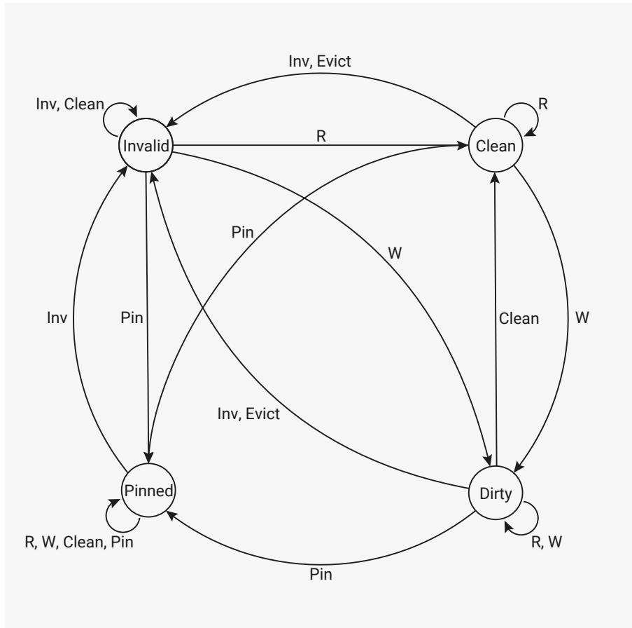
The changes to a cache line caused by cached accesses and maintenance operations can be summarised by a set of state transitions.
Figure 17. State transition diagram for each cache line. Inv , Clean and Pin represent invalidate/clean/pin maintenance operations, respectively. R and W represent cached reads and writes. Evict represents a cache line deallocation to make room for a new allocation due to a read/write cache miss.
graph TD
    Invalid((Invalid))
    Clean((Clean))
    Pinned((Pinned))
    Dirty((Dirty))

    Invalid -- "Inv, Clean" --> Invalid
    Invalid -- "Inv, Evict" --> Clean
    Invalid -- "Pin" --> Pinned
    Invalid -- "R" --> Clean
    Invalid -- "W" --> Dirty
    Clean -- "R" --> Clean
    Clean -- "W" --> Dirty
    Clean -- "Clean" --> Clean
    Clean -- "Inv, Evict" --> Invalid
    Pinned -- "Inv" --> Invalid
    Pinned -- "R, W, Clean, Pin" --> Pinned
    Dirty -- "R, W" --> Dirty
    Dirty -- "Pin" --> Pinned
    Dirty -- "Clean" --> Clean
    Dirty -- "Inv, Evict" --> Invalid
Initially, the state of all cache lines is undefined. When booting from flash, the bootrom performs an invalidate by set/way on every line of the cache to force them to a known state. In the diagram above, all states have an Inv arc to the invalid state.
A dirty cache line contains data not yet propagated to downstream memory.
A clean cache line contains data that matches the downstream memory contents.
Accessing an invalid cache line causes an allocation : the cache fetches the corresponding data from downstream memory, stores it in the cache, then marks the cache line as clean or dirty. The cache also stores part of the downstream address, known as the tag , to recall the downstream address stored in each cache line. Read allocations enter the clean state, so the cache line can be safely freed at any time. Write allocations enter the dirty state, so the cache line must propagate downstream before it can be freed.
Writing to a clean cache line marks it as dirty because the cache now contains write data that has not propagated downstream. The line can be explicitly returned to the clean state using a clean maintenance operation ( 0x1 or 0x3 ), but this is not required. Typically, the cache automatically propagates dirty cache lines downstream when it needs to reallocate them.
Evictions happen when a cached read or write needs to allocate a cache line that is already in the clean or dirty state. The eviction transitions the line momentarily to the invalid state, ready for allocation. For clean cache lines, this happens instantaneously. For dirty cache lines, the cache must first propagate the cache line contents downstream before it can safely enter the invalid state.
Cache lines enter the pinned state using a pin maintenance operation ( 0x7 ) and exit only by an invalidate maintenance operation ( 0x0 or 0x2 ).
NOTEThe pin maintenance operation only marks the line as pinned; it does not perform any copying of data. When pinning lines that exist in external memory devices, you must first pin the line, then copy the downstream data into the pinned line by reading from the uncached XIP window.
4.4.1.3. Cache-as-SRAMWhen you disabled the cache of RP2040, the cache would map the entire cache memory at
0x15000000
. RP2350 replaces this with the ability to pin individual cache lines. You can use this in the following ways:
- • Pin the entire cache at some address range to use the entire cache as SRAM
- • Pin one full cache way to make half of the cache available for cache-as-SRAM use (the remaining cache way still functions as usual)
- • Pin an address range that maps critical flash contents
Pinned cache lines are not accessible when the cache is disabled via the
CTRL
register (
CTRL.EN_SECURE
or
CTRL.EN_NONSECURE
depending on security level of the bus access).
Because the QMI only occupies the lower half of the 64 MB XIP address space, you can pin cache lines outside of the QMI address range (e.g. at the top of the XIP space) to avoid interfering with any QMI accesses. As a general rule, the more cache you pin, the lower the cache hit rate for other accesses.
Cache lines are pinned using the pin maintenance operation (
0x7
), which performs the following steps:
- 1. An implicit invalidate-by-address operation (
0x2) using the full address of the maintenance operation- ◦ This ensures that each address is allocated in only one cache way (required for correct cache operation)
- 2. Select the cache line to be pinned, using bit
13to select the cache way, and bits12:3to select the cache set (as with0x0/0x1invalidate/clean by set/way commands) - 3. Write the address to the cache line's tag entry
- 4. Change the cache line's state to pinned (as per the state diagram in Section 4.4.1.2 )
- 5. Update the cache line's tag with the full address of the maintenance operation
After a pin operation, cached reads and writes to the specified address always hit the cache until that cache line is either invalidated or pinned to a different address.
NOTEPinning two addresses that are equal modulo cache size pins the same cache line twice. It does not pin two different cache lines. The second pin will overwrite the first.
When a cached access hits a pinned cache line, it behaves the same as a dirty line. The cache reads and writes as if allocated in the cache by normal means.
Cache eviction policy is random, and the cache only makes one attempt to select an eviction way. If the cache selects to evict a pinned line, the eviction fails, and the access is demoted to an uncached access. As a result, a cache with one way pinned does not behave exactly the same as a direct-mapped 8 kB cache, but average-case performance is similar.
Cache line states are stored in the cache tag memory stored in the XIP memory power domain. This memory contents do not change on reset, so pinned lines remain pinned across resets. If the XIP memory power domain is not powered down, memory contents do not change across power cycles of the switched core reset domain. The bootrom clears the tag memory upon entering the flash boot or NSBOOT (USB boot) path, but watchdog scratch vector reboots can boot directly into pinned XIP cache lines.
4.4.2. QSPI Memory Interface (QMI)
Uncached accesses and cache misses require access to external memory. The QSPI memory interface (QMI) provides this access, as documented in Section 12.14 . The QMI supports:
- • Up to two external QSPI devices, with separate chip selects and shared clock/data pins
- ◦ Banked configuration registers, including different SCK frequencies and QSPI opcodes
- • Memory-mapped reads and writes (writes must be enabled via CTRL.WRITABLE_M0/CTRL.WRITABLE_M1 )
- • Serial/dual/quad-SPI transfer formats
- • SCK speeds as high as clk_sys
- • 8/16/32-bit accesses for uncached accesses, and 64-bit accesses for cache line fills
- • Automatic chaining of sequentially addressed accesses into a single QSPI transfer
- • Address translation (4 × 4 MB windows per QSPI device)
- ◦ Flash storage addresses can differ from runtime addresses, e.g. for multiple OTA upgrade image slots
- ◦ Allows code and data segments, or Secure and Non-secure images, to be mapped separately
- • Direct-mode FIFO interface for programming and configuring external QSPI devices
XIP accesses via the two cache AHB ports, and from the DMA streaming hardware, arbitrate for access to the QMI. A separate APB port configures the QMI.
The QMI is a new memory interface designed for RP2350, replacing the SSI peripheral on RP2040.
4.4.3. Streaming DMA interface
As the flash is generally much larger than on-chip SRAM, it's often useful to stream chunks of data into memory from flash. It's convenient to have the DMA stream this data in the background while software in the foreground does other things. It's even more convenient if code can continue to execute from flash whilst this takes place.
This doesn't interact well with standard XIP operation because QMI serial transfers force lengthy bus stalls on the DMA. These stalls are tolerable for a processor because an in-order processor tends to have nothing better to do while waiting for an instruction fetch to retire, and because typical code execution tends to have much higher cache hit rates than bulk streaming of infrequently accessed data. In contrast, stalling the DMA prevents any other active DMA channels from making progress during this time, slowing overall DMA throughput.
The STREAM_ADDR and STREAM_CTR registers are used to program a linear sequence of flash reads. The XIP subsystem performs these reads in the background in a best-effort fashion. To minimise impact on code executed from flash whilst the stream is ongoing, the streaming hardware has lower priority access to the QMI than regular XIP accesses, and there is a brief cooldown (9 cycles) between the last XIP cache miss and resuming streaming. This avoids increases in initial access latency on XIP cache misses.
Pico Examples: https://github.com/raspberrypi/pico-examples/blob/master/flash/xip_stream/flash_xip_stream.c Lines 45 - 48
45     while (!(xip_ctrl_hw->stat & XIP_STAT_FIFO_EMPTY))
46         (void) xip_ctrl_hw->stream_fifo;
47     xip_ctrl_hw->stream_addr = (uint32_t) &random_test_data[0];
48     xip_ctrl_hw->stream_ctr = count_of(random_test_data);
The streamed data is pushed to a small FIFO, which generates DREQ signals that tell the DMA to collect the streamed data. As the DMA does not initiate a read until after reading the data from flash, the DMA does not stall when accessing the data. The DMA can then retrieve this data through the auxiliary AHB port, which provides direct single-cycle access to the streaming data FIFO.
On RP2350, you can also use the auxiliary AHB port to access the QMI direct-mode FIFOs. This is faster than accessing
the FIFOs through the QMI APB configuration port. When QMI access chaining is enabled, the streaming XIP DMA is close to the maximum theoretical QSPI throughput, but the direct-mode FIFOs are available on AHB for situations that require 100% of the theoretical throughput.
Pico Examples: https://github.com/raspberrypi/pico-examples/blob/master/flash/xip_stream/flash_xip_stream.c Lines 58 - 70
58     const uint dma_chan = 0;
59     dma_channel_config cfg = dma_channel_get_default_config(dma_chan);
60     channel_config_set_read_increment(&cfg, false);
61     channel_config_set_write_increment(&cfg, true);
62     channel_config_set_dreq(&cfg, DREQ_XIP_STREAM);
63     dma_channel_configure(
64         dma_chan,
65         &cfg,
66         (void *) buf,           // Write addr
67         (const void *) XIP_AUX_BASE, // Read addr
68         count_of(random_test_data), // Transfer count
69         true                    // Start immediately!
70     );
4.4.4. Performance counters
The XIP subsystem provides two performance counters. These are 32 bits in size, saturate upon reaching 0xffffffff, and are cleared by writing any value. They count:
- 1. The total number of XIP accesses, to any alias
- 2. The number of XIP accesses that resulted in a cache hit
This provides a way to profile the cache hit rate for common use cases.
4.4.5. List of XIP_CTRL registers
The XIP control registers start at a base address of 0x400c8000 (defined as XIP_CTRL_BASE in SDK).
Table 439. List of XIP registers
| Offset | Name | Info |
|---|---|---|
| 0x00 | CTRL | Cache control register. Read-only from a Non-secure context. |
| 0x08 | STAT | |
| 0x0c | CTR_HIT | Cache Hit counter |
| 0x10 | CTR_ACC | Cache Access counter |
| 0x14 | STREAM_ADDR | FIFO stream address |
| 0x18 | STREAM_CTR | FIFO stream control |
| 0x1c | STREAM_FIFO | FIFO stream data |
XIP: CTRL Register
Offset: 0x00
Description
Cache control register. Read-only from a Non-secure context.
Table 440. CTRL Register
| Bits | Description | Type | Reset |
|---|---|---|---|
| 31:12 | Reserved. | - | - |
| 11 | WRITABLE_M1: If 1, enable writes to XIP memory window 1 (addresses 0x11000000 through 0x11ffffff, and their uncached mirrors). If 0, this region is read-only. XIP memory is read-only by default . This bit must be set to enable writes if a RAM device is attached on QSPI chip select 1. The default read-only behaviour avoids two issues with writing to a read-only QSPI device (e.g. flash). First, a write will initially appear to succeed due to caching, but the data will eventually be lost when the written line is evicted, causing unpredictable behaviour. Second, when a written line is evicted, it will cause a write command to be issued to the flash, which can break the flash out of its continuous read mode. After this point, flash reads will return garbage. This is a security concern, as it allows Non-secure software to break Secure flash reads if it has permission to write to any flash address. Note the read-only behaviour is implemented by downgrading writes to reads, so writes will still cause allocation of an address, but have no other effect. | RW | 0x0 |
| 10 | WRITABLE_M0: If 1, enable writes to XIP memory window 0 (addresses 0x10000000 through 0x10ffffff, and their uncached mirrors). If 0, this region is read-only. XIP memory is read-only by default . This bit must be set to enable writes if a RAM device is attached on QSPI chip select 0. The default read-only behaviour avoids two issues with writing to a read-only QSPI device (e.g. flash). First, a write will initially appear to succeed due to caching, but the data will eventually be lost when the written line is evicted, causing unpredictable behaviour. Second, when a written line is evicted, it will cause a write command to be issued to the flash, which can break the flash out of its continuous read mode. After this point, flash reads will return garbage. This is a security concern, as it allows Non-secure software to break Secure flash reads if it has permission to write to any flash address. Note the read-only behaviour is implemented by downgrading writes to reads, so writes will still cause allocation of an address, but have no other effect. | RW | 0x0 |
| 9 | SPLIT_WAYS: When 1, route all cached+Secure accesses to way 0 of the cache, and route all cached+Non-secure accesses to way 1 of the cache. This partitions the cache into two half-sized direct-mapped regions, such that Non-secure code can not observe cache line state changes caused by Secure execution. A full cache flush is required when changing the value of SPLIT_WAYS. The flush should be performed whilst SPLIT_WAYS is 0, so that both cache ways are accessible for invalidation. | RW | 0x0 |
| Bits | Description | Type | Reset |
|---|---|---|---|
| 8 | MAINT_NONSEC: When 0, Non-secure accesses to the cache maintenance address window ( \( \text{addr}[27] == 1, \text{addr}[26] == 0 \) ) will generate a bus error. When 1, Non-secure accesses can perform cache maintenance operations by writing to the cache maintenance address window. Cache maintenance operations may be used to corrupt Secure data by invalidating cache lines inappropriately, or map Secure content into a Non-secure region by pinning cache lines. Therefore this bit should generally be set to 0, unless Secure code is not using the cache. Care should also be taken to clear the cache data memory and tag memory before granting maintenance operations to Non-secure code. | RW | 0x0 |
| 7 | NO_UNTRANSLATED_NONSEC: When 1, Non-secure accesses to the uncached, untranslated window ( \( \text{addr}[27:26] == 3 \) ) will generate a bus error. | RW | 0x1 |
| 6 | NO_UNTRANSLATED_SEC: When 1, Secure accesses to the uncached, untranslated window ( \( \text{addr}[27:26] == 3 \) ) will generate a bus error. | RW | 0x0 |
| 5 | NO_UNCACHED_NONSEC: When 1, Non-secure accesses to the uncached window ( \( \text{addr}[27:26] == 1 \) ) will generate a bus error. This may reduce the number of SAU/MPU/PMP regions required to protect flash contents. Note this does not disable access to the uncached, untranslated window – see NO_UNTRANSLATED_SEC. | RW | 0x0 |
| 4 | NO_UNCACHED_SEC: When 1, Secure accesses to the uncached window ( \( \text{addr}[27:26] == 1 \) ) will generate a bus error. This may reduce the number of SAU/MPU/PMP regions required to protect flash contents. Note this does not disable access to the uncached, untranslated window – see NO_UNTRANSLATED_SEC. | RW | 0x0 |
| 3 | POWER_DOWN: When 1, the cache memories are powered down. They retain state, but can not be accessed. This reduces static power dissipation. Writing 1 to this bit forces CTRL_EN_SECURE and CTRL_EN_NONSECURE to 0, i.e. the cache cannot be enabled when powered down. | RW | 0x0 |
| 2 | Reserved. | - | - |
| 1 | EN_NONSECURE: When 1, enable the cache for Non-secure accesses. When enabled, Non-secure XIP accesses to the cached ( \( \text{addr}[26] == 0 \) ) window will query the cache, and QSPI accesses are performed only if the requested data is not present. When disabled, Secure access ignore the cache contents, and always access the QSPI interface. Accesses to the uncached ( \( \text{addr}[26] == 1 \) ) window will never query the cache, irrespective of this bit. | RW | 0x1 |
| Bits | Description | Type | Reset |
|---|---|---|---|
| 0 | EN_SECURE: When 1, enable the cache for Secure accesses. When enabled, Secure XIP accesses to the cached (addr[26] == 0) window will query the cache, and QSPI accesses are performed only if the requested data is not present. When disabled, Secure access ignore the cache contents, and always access the QSPI interface. Accesses to the uncached (addr[26] == 1) window will never query the cache, irrespective of this bit. There is no cache-as-SRAM address window. Cache lines are allocated for SRAM-like use by individually pinning them, and keeping the cache enabled. | RW | 0x1 |
XIP: STAT Register
Offset: 0x08
Table 441. STAT Register
| Bits | Description | Type | Reset |
|---|---|---|---|
| 31:3 | Reserved. | - | - |
| 2 | FIFO_FULL: When 1, indicates the XIP streaming FIFO is completely full. The streaming FIFO is 2 entries deep, so the full and empty flag allow its level to be ascertained. | RO | 0x0 |
| 1 | FIFO_EMPTY: When 1, indicates the XIP streaming FIFO is completely empty. | RO | 0x1 |
| 0 | Reserved. | - | - |
XIP: CTR_HIT Register
Offset: 0x0c
Description
Cache Hit counter
Table 442. CTR_HIT Register
| Bits | Description | Type | Reset |
|---|---|---|---|
| 31:0 | A 32 bit saturating counter that increments upon each cache hit, i.e. when an XIP access is serviced directly from cached data. Write any value to clear. | WC | 0x00000000 |
XIP: CTR_ACC Register
Offset: 0x10
Description
Cache Access counter
Table 443. CTR_ACC Register
| Bits | Description | Type | Reset |
|---|---|---|---|
| 31:0 | A 32 bit saturating counter that increments upon each XIP access, whether the cache is hit or not. This includes noncacheable accesses. Write any value to clear. | WC | 0x00000000 |
XIP: STREAM_ADDR Register
Offset: 0x14
Description
FIFO stream address
Table 444.
STREAM_ADDR
Register
| Bits | Description | Type | Reset |
|---|---|---|---|
| 31:2 | The address of the next word to be streamed from flash to the streaming FIFO. Increments automatically after each flash access. Write the initial access address here before starting a streaming read. | RW | 0x00000000 |
| 1:0 | Reserved. | - | - |
XIP: STREAM_CTR Register
Offset: 0x18
Description
FIFO stream control
Table 445.
STREAM_CTR Register
| Bits | Description | Type | Reset |
|---|---|---|---|
| 31:22 | Reserved. | - | - |
| 21:0 | Write a nonzero value to start a streaming read. This will then progress in the background, using flash idle cycles to transfer a linear data block from flash to the streaming FIFO. Decrements automatically (1 at a time) as the stream progresses, and halts on reaching 0. Write 0 to halt an in-progress stream, and discard any in-flight read, so that a new stream can immediately be started (after draining the FIFO and reinitialising STREAM_ADDR) | RW | 0x000000 |
XIP: STREAM_FIFO Register
Offset: 0x1c
Description
FIFO stream data
Table 446.
STREAM_FIFO
Register
| Bits | Description | Type | Reset |
|---|---|---|---|
| 31:0 | Streamed data is buffered here, for retrieval by the system DMA. This FIFO can also be accessed via the XIP_AUX slave, to avoid exposing the DMA to bus stalls caused by other XIP traffic. | RF | 0x00000000 |
4.4.6. List of XIP_AUX registers
The XIP_AUX port provides fast AHB access to the streaming FIFO and the QMI Direct Mode FIFOs, to reduce the cost of DMA access to these FIFOs.
Table 447. List of
XIP_AUX registers
| Offset | Name | Info |
|---|---|---|
| 0x0 | STREAM | Read the XIP stream FIFO (fast bus access to XIP_CTRL_STREAM_FIFO) |
| 0x4 | QMI_DIRECT_TX | Write to the QMI direct-mode TX FIFO (fast bus access to QMI_DIRECT_TX) |
| Offset | Name | Info |
|---|---|---|
| 0x8 | QMI_DIRECT_RX | Read from the QMI direct-mode RX FIFO (fast bus access to QMI_DIRECT_RX) |
XIP_AUX: STREAM Register
Offset: 0x0
Table 448. STREAM Register
| Bits | Description | Type | Reset |
|---|---|---|---|
| 31:0 | Read the XIP stream FIFO (fast bus access to XIP_CTRL_STREAM_FIFO) | RF | 0x00000000 |
XIP_AUX: QMI_DIRECT_TX Register
Offset: 0x4
Description
Write to the QMI direct-mode TX FIFO (fast bus access to QMI_DIRECT_TX)
Table 449. QMI_DIRECT_TX Register
| Bits | Description | Type | Reset |
|---|---|---|---|
| 31:21 | Reserved. | - | - |
| 20 | NOPUSH
: Inhibit the RX FIFO push that would correspond to this TX FIFO entry. Useful to avoid garbage appearing in the RX FIFO when pushing the command at the beginning of a SPI transfer. | WF | 0x0 |
| 19 | OE
: Output enable (active-high). For single width (SPI), this field is ignored, and SD0 is always set to output, with SD1 always set to input. For dual and quad width (DSPI/QSPI), this sets whether the relevant SDx pads are set to output whilst transferring this FIFO record. In this case the command/address should have OE set, and the data transfer should have OE set or clear depending on the direction of the transfer. | WF | 0x0 |
| 18 | DWIDTH : Data width. If 0, hardware will transmit the 8 LSBs of the DIRECT_TX DATA field, and return an 8-bit value in the 8 LSBs of DIRECT_RX. If 1, the full 16-bit width is used. 8-bit and 16-bit transfers can be mixed freely. | WF | 0x0 |
| 17:16 | IWIDTH : Configure whether this FIFO record is transferred with single/dual/quad interface width (0/1/2). Different widths can be mixed freely. | WF | 0x0 |
| Enumerated values: | |||
| 0x0 → S: Single width | |||
| 0x1 → D: Dual width | |||
| 0x2 → Q: Quad width | |||
| 15:0 | DATA
: Data pushed here will be clocked out falling edges of SCK (or before the very first rising edge of SCK, if this is the first pulse). For each byte clocked out, the interface will simultaneously sample one byte, on rising edges of SCK, and push this to the DIRECT_RX FIFO. For 16-bit data, the least-significant byte is transmitted first. | WF | 0x0000 |
XIP_AUX: QMI_DIRECT_RX Register
Offset: 0x8
Description
Read from the QMI direct-mode RX FIFO (fast bus access to QMI_DIRECT_RX)
Table 450.
QMI_DIRECT_RX
Register
| Bits | Description | Type | Reset |
|---|---|---|---|
| 31:16 | Reserved. | - | - |
| 15:0 | With each byte clocked out on the serial interface, one byte will simultaneously be clocked in, and will appear in this FIFO. The serial interface will stall when this FIFO is full, to avoid dropping data. When 16-bit data is pushed into the TX FIFO, the corresponding RX FIFO push will also contain 16 bits of data. The least-significant byte is the first one received. | RF | 0x0000 |
4.5. OTP
RP2350 contains 8 kB of one-time-programmable storage (OTP), which stores:
- • Manufacturing information such as unique device ID
- • Boot configuration such as non-default crystal oscillator frequency
- • Public key fingerprint(s) for boot signature enforcement
- • Symmetric keys for decryption of external flash contents into SRAM
- • User-defined contents, including bootable program images ( Section 5.10.7 )
The OTP storage is structured as 4096 × 24-bit rows. Each row contains 16 bits of data and 8 bits of parity information, providing 8 kB of data storage. OTP bit cells are initially 0 and can be programmed to 1. However, they cannot be cleared back to 0 under any circumstance. This ensures that security-critical flags, such as debug disables, are physically impossible to clear once set. However, you must also take care to program the correct values.
For more information about the OTP subsystem, see Chapter 13 .