6. Power
6.1. Power supplies
RP2350 requires five separate power supplies. However, in most applications, several of these can be combined and connected to a single power source. Typical applications only require a single 3.3 V supply. See Figure 19 .
The power supplies and a number of potential power supply schemes are described in the following sections. Detailed power supply parameters are provided in Section 14.9.5 .
6.1.1. Digital IO supply (IOVDD)
IOVDD provides the IO supply for the chip's GPIO, and should be powered at a nominal voltage between 1.8 V and 3.3 V. The supply voltage sets the external signal level for the digital IO, and should be chosen based on the level required, see Section 14.9 for details. All GPIOs share the same power supply and operate at the same signal level.
If the digital IO is powered at a nominal 1.8 V, the IO input thresholds should be adjusted by setting the VOLTAGE_SELECT register to 1. VOLTAGE_SELECT is set to 0 by default, which results in input thresholds that are valid for a nominal IO voltage between 2.5 V and 3.3 V. See Chapter 9 for details.
⚠ CAUTION
Powering the IOVDD at 1.8 V with input thresholds set for a 2.5 V to 3.3 V supply is a safe operating mode, but will result in input thresholds that do not meet specification. Powering the IO at voltages greater than 1.8 V with input thresholds set for a 1.8 V supply may result in damage to the chip.
6.1.2. QSPI IO supply (QSPI_IOVDD)
QSPI_IOVDD provides the IO supply for the chip's QSPI interface, and should be powered at a nominal voltage between 1.8 V and 3.3 V. The supply voltage sets the external signal level for the QSPI interface, and should be chosen based on the level required, see Section 14.9 for details. In most applications the QSPI interface will be connected to an external flash device, which will determine the required signal level.
If the QSPI interface is powered at a nominal 1.8 V, the IO input thresholds should be adjusted by setting the VOLTAGE_SELECT register to 1. VOLTAGE_SELECT is set to 0 by default, which results in input thresholds that are valid for a nominal IO voltage between 2.5 V and 3.3 V. See Chapter 9 for details.
⚠ CAUTION
Powering the IOVDD at 1.8 V with input thresholds set for a 2.5 V to 3.3 V supply is a safe operating mode, but will result in input thresholds that do not meet specification. Powering the IO at voltages greater than 1.8 V with input thresholds set for a 1.8 V supply may result in damage to the chip.
6.1.3. Digital core supply (DVDD)
The chip's core digital logic is powered by DVDD, which should be at a nominal 1.1 V. A dedicated on-chip core voltage regulator allows DVDD to be generated from a 2.7 V to 5.5 V input supply. See Section 6.3 for details. Alternatively, DVDD can be supplied directly from an off-chip power source.
If the on-chip core voltage regulator is used, the two DVDD pins closest to the regulator should be decoupled with a 100nF capacitor close to the pins. The DVDD pin furthest from the regulator should be decoupled with a 4.7μF capacitor close to
the pin.
6.1.4. USB PHY and OTP supply (USB_OTP_VDD)
USB_OTP_VDD supplies the chip's USB PHY and OTP memory, and should be powered at a nominal 3.3 V. To reduce the number of external power supplies, USB_OTP_VDD can use the same power source as the core voltage regulator analogue supply (VREG_AVDD), or digital IO supply (IOVDD), assuming IOVDD is also powered at 3.3 V. This supply must always be provided, even in applications where the USB PHY is never used.
USB_OTP_VDD should be decoupled with a 100nF capacitor close to the chip's USB_OTP_VDD pin.
6.1.5. ADC supply (ADC_AVDD)
ADC_AVDD supplies the chip's Analogue to Digital Converter (ADC). It can be powered at a nominal voltage between 1.8 V and 3.3 V, but the performance of the ADC will be compromised at voltages below 2.97 V. To reduce the number of external power supplies, ADC_AVDD can use the same power source as the core voltage regulator analogue supply (VREG_AVDD) or digital IO supply (IOVDD).
NOTE
It is safe to supply ADC_AVDD at a higher or lower voltage than IOVDD, e.g. to power the ADC at 3.3 V, for optimum performance, while supporting 1.8 V signal levels on the digital IO. But the voltage on the ADC analogue inputs must not exceed IOVDD, e.g. if IOVDD is powered at 1.8 V, the voltage on the ADC inputs should be limited to 1.8 V. Voltages greater than IOVDD will result in leakage currents through the ESD protection diodes. See Section 14.9 for details.
ADC_AVDD should be decoupled with a 100nF capacitor close to the chip's ADC_AVDD pin.
6.1.6. Core voltage regulator input supply (VREG_VIN)
VREG_VIN is the input supply for the on-chip core voltage regulator, and should be in the range 2.7 V to 5.5 V. To reduce the number of external power supplies, VREG_VIN can use the same power source as the voltage regulator analogue supply (VREG_AVDD), or digital IO supply (IOVDD). Though care should be taken to minimise the noise on VREG_AVDD.
A 4.7µF capacitor should be connected between VREG_VIN and ground close to the chip's VREG_VIN pin.
For more details on the on-chip voltage regulator see Section 6.3 .
6.1.7. On-chip voltage regulator analogue supply (VREG_AVDD)
VREG_AVDD supplies the on chip voltage regulator's analogue control circuits, and should be powered at a nominal 3.3 V. To reduce the number of external power supplies, VREG_AVDD can use the same power source as the voltage regulator input supply (VREG_VIN), or the digital IO supply (IOVDD). Though care should be taken to minimise the noise on VREG_AVDD. A passive low pass filter may be required, see Section 6.3.7 for details.
NOTE
VREG_AVDD also powers the chip's power-on reset and brownout detection blocks, so it must be powered even if the on-chip voltage regulator is not used.
6.1.8. Power supply sequencing
With the exception of the two voltage regulator supplies ( VREG_VIN and VREG_AVDD ), which should be powered up together, RP2350's power supplies may be powered up or down in any order. However, small transient currents may flow in the ADC supply ( ADC_AVDD ) if it is powered up before, or powered down after, the digital core supply (DVDD). This will not damage the chip, but can be avoided by powering up DVDD before or at the same time as ADC_AVDD , and powering down DVDD after or at the same time as ADC_AVDD . In the most common power supply scheme, where the chip is powered from a single 3.3 V supply, DVDD will be powered up shortly after ADC_AVDD due to the startup time of the on-chip voltage regulator. This is acceptable behaviour.
6.2. Power management
RP2350 retains the power control features of RP2040, but extends them by splitting the chip's digital core into a number of power domains, which can be selectively powered off. This allows significant power saving in applications where the chip is not continuously active. This section describes the core power domains and how they are controlled. The legacy RP2040 power control features still offer useful power savings, and are described in Section 6.5 .
Power domains, and transitions between power states, are controlled by a Power manager. The Power manager runs from either an internal low power oscillator lposc , or the reference clock clk_ref . The device may be configured to power down under software control and can wakeup on a GPIO or timer event. Configuration of the power manager is via the POWMAN registers in Section 6.4 .
6.2.1. Core power domains
RP2350's core logic is divided into five power domains. With some restrictions, these domains can be selectively powered off to reduce the chip's power consumption. The five domains are:
- • AON - Always On - a small amount of logic that is always powered on when chip's core supply ( DVDD ) is available
- • SWCORE - Switched Core - the remaining core logic functions, including processors, bus fabric, peripherals, etc.
- • XIP - XIP cache SRAM and Boot RAM
- • SRAM0 - SRAM Power Domain 0 - the lower half of the large SRAM banks
- • SRAM1 - SRAM Power Domain 1 - the upper half of the large SRAM banks, and the scratch SRAMs
Logic in the AON domain controls the power state of the other power domains, which can be powered on or off independently. The only exception is the XIP domain, which must always be powered when the SWCORE domain is powered. SRAMs that are powered on retain their contents when the switched core is powered off.
Figure 18 gives an overview of the core power domains.
Figure 18. core power domains
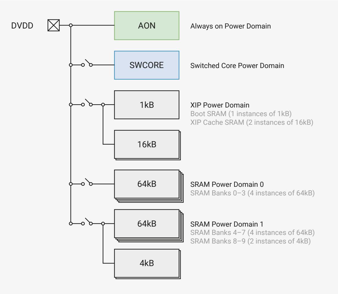
The diagram illustrates the core power domains of the RP2350. A DVDD supply line is shown on the left, branching into several domains:
- AON (Always on Power Domain): Represented by a green box.
- SWCORE (Switched Core Power Domain): Represented by a blue box.
- XIP Power Domain : Contains a 1kB Boot SRAM (1 instance of 1kB) and 16kB XIP Cache SRAM (2 instances of 16kB).
- SRAM Power Domain 0 : Contains 64kB SRAM Banks 0–3 (4 instances of 64kB).
- SRAM Power Domain 1 : Contains 64kB SRAM Banks 4–7 (4 instances of 64kB) and 4kB SRAM Banks 8–9 (2 instances of 4kB).
- 4kB : A separate domain at the bottom.
6.2.2. Power states
RP2350 can operate in a number of power states, depending on which domains are powered on or off. Power states have names in the form Pc.m where:
- • c indicates the state of the switched core (SWCORE) domain: 0 = on / 1 = off
- • m is a 3 bit binary representation of the memory power domains, in the order XIP, SRAM0, SRAM1
P0.m states, where the switched core is powered on, are Normal Operating states. P1.m states, where the switched core is powered off, are Low Power states
Table 475 shows the available power states.
Table 475. supported power states
| Power State | Description | AON | SWCORE | XIP | SRAM0 | SRAM1 |
|---|---|---|---|---|---|---|
| P0.0 | Normal Operation | on | on | on | on | on |
| P0.1 | Normal Operation (SRAM1 off) | on | on | on | on | off |
| P0.2 | Normal Operation (SRAM0 off) | on | on | on | off | on |
| P0.3 | Normal Operation (SRAM0 & SRAM1 off) | on | on | on | off | off |
| P1.0 | Low Power | on | off | on | on | on |
| P1.1 | Low Power (SRAM1 off) | on | off | on | on | off |
| P1.2 | Low Power (SRAM0 off) | on | off | on | off | on |
| Power State | Description | AON | SWCORE | XIP | SRAM0 | SRAM1 |
|---|---|---|---|---|---|---|
| P1.3 | Low Power (SRAM0 & SRAM1 off) | on | off | on | off | off |
| P1.4 | Low Power (XIP off) | on | off | off | on | on |
| P1.5 | Low Power (XIP & SRAM1 off) | on | off | off | on | off |
| P1.6 | Low Power (XIP & SRAM0 off) | on | off | off | off | on |
| P1.7 | Low Power (XIP & SRAM0 & SRAM1 off) | on | off | off | off | off |
| OFF | Not Powered | off | off | off | off | off |
In the OFF state, the chip has no external power and all domains are unpowered. The chip moves from OFF to P0.0 automatically as soon as external power is applied.
To determine the current power state, read the STATE.CURRENT field. CURRENT is a 4 bit field representing the power state of the switched core and memory power domains.
6.2.3. Power state transitions
Transitions between power states can be initiated by software, hardware, or via the chip's debug subsystem. After initiation, transitions are managed by autonomous power sequencers in the chip's AON power domain. The power sequencers can be configured, in a limited way, via the SEQ_CFG register. The sequencers can also be observed and controlled, again in a limited way, via the RP-AP registers in the chip's debug subsystem. These registers are described in Section 3.5.10 .
Valid power state transitions are as follows:
- all transitions from one P0.m state (switched core powered on) to another P0.m state (switched core powered on), if they increase or decrease the number of SRAM domains that are powered on
- all transitions from a P0.m state (switched core powered on) to a P1.m state (switched core powered off), except transitions that would result in a powered off SRAM domain becoming powered on
- all transitions from a P1.m state (switched core powered off) to a P0.m state (switched core powered on), except transitions that would result in a powered on SRAM domain becoming powered off
Transitions from one P1.m state (switched core powered off) to another P1.m state (switched core powered off) are not supported, and will be prevented by the hardware.
Valid transitions are shown in the table below.
Table 476. valid power state transitions
| From | To | |||||||||||
|---|---|---|---|---|---|---|---|---|---|---|---|---|
| P0.0 | P0.1 | P0.2 | P0.3 | P1.0 | P1.1 | P1.2 | P1.3 | P1.4 | P1.5 | P1.6 | P1.7 | |
| P0.1 | P0.0 | P0.3 | P1.1 | P1.3 | P1.5 | P1.7 | ||||||
| P0.2 | P0.0 | P0.3 | P1.2 | P1.3 | P1.6 | P1.7 | ||||||
| P0.3 | P0.0 | P0.1 | P0.2 | P1.3 | P1.7 | |||||||
| P1.0 | P0.0 | |||||||||||
| P1.1 | P0.0 | P0.1 | ||||||||||
| P1.2 | P0.0 | P0.2 | ||||||||||
| P1.3 | P0.0 | P0.1 | P0.2 | P0.3 | ||||||||
| P1.4 | P0.0 | |||||||||||
| P1.5 | P0.0 | P0.1 | ||||||||||
| From | To | |||||||||||
|---|---|---|---|---|---|---|---|---|---|---|---|---|
| P1.6 | P0.0 | P0.2 | ||||||||||
| P1.7 | P0.0 | P0.1 | P0.2 | P0.3 | ||||||||
6.2.3.1. Transitions from Normal Operating (P0.m) states
Transitions from a Normal Operating (P0.m) state to either a Low Power (P1.m) state, or another Normal Operating (P0.m) state, are initiated by writing to the STATE.REQ field. REQ is a 4-bit field representing the requested power state of the switched core and memory power domains. The STATE.WAITING field will be set immediately, followed by the STATE.CHANGING field, after the actual state change starts. If a transition to a Low Power (P1.m) state is requested, WAITING will remain set until the processors have gone into a low power state (via __wfi() ). In the WAITING state, writing to the STATE.REQ field can change or cancel the initial request. The requested state can't be changed when in the CHANGING state.
A request to move to an unsupported state, or a state that would result in an invalid transition, causes the STATE.BAD_SW_REQ field to be set.
If a hardware power up request is received while in the WAITING state, the transition requested via STATE.REQ will be halted and the power up request completed. The STATE.PWRUP_WHILE_WAITING and STATE.REQ_IGNORED fields will be set.
On writing to STATE.REQ :
- • If there is a pending power up request, STATE.REQ_IGNORED is set and no further action is taken
- • If the requested state is invalid, STATE.BAD_SW_REQ is set and no further action is taken
- • If the switched core is being powered off,
STATE.WAITING
is set until both processors enter
__wfi()
. After which
STATE.CHANGING
will be set, but no processors will be powered up to read the flag at this time
- ◦ If there is a power up request while in STATE.WAITING , STATE.PWRUP_WHILE_WAITING is set, which can also raise an interrupt to bring the processors out of __wfi() . No further action is taken
- ◦ You can get out of the WAITING state by writing a new request to STATE.REQ before both processors have gone into __wfi()
- • Any state request that isn't powering down the switched core, such as powering up or down SRAM domain 0 or 1 starts immediately. Software should wait until STATE.CHANGING has cleared to know the power down sequence. After the STATE.CHANGING flag is cleared STATE.CURRENT is updated.
- • If powering up, software should also wait for STATE.CHANGING to make sure everything is powered up before continuing. In practice this is handled by the RP2350 bootrom.
Invalid state transitions are:
- • any combination of power up and power down requests
- • any request which would result in power down of XIP/bootRAM and power up of SWCORE
If XIP, boot RAM, sram0, or sram1 remain powered while SWCORE is powered off, the sram will automatically switch to a low power state. Stored data will be retained.
Before transitioning to a switched-core power down state (P1.m), software needs to configure:
- • the GPIO wakeup conditions if required
- • the wakeup alarm if required
- • the return state of the SRAM0 & SRAM1 domains
6.2.3.2. Transitions from Low Power (P1.m) states
Transitions from P1.m to P0.m states are initiated by GPIO events or the timer alarm.
There are up to 5 wakeup sources:
- • up to 4 GPIO wakeups (level high/low or falling edge/rising edge)
- • 1 alarm wakeup
GPIO wakeups are configured by the PWRUP0-PWRUP3 registers. The wakeups are not enabled until the power sequencer completes the power down operation.
The alarm wakeup is configured by writing to the ALARM_TIME_15T00-ALARM_TIME_63T048 registers. The alarm wakeup has a resolution of 1ms. Once set, the alarm wakeup is armed by writing a 1 to both TIMER.PWRUP_ON_ALARM and TIMER.ALARM_ENAB . If the alarm fires during the power down sequence, a power up sequence will start when the power down sequence completes.
The LAST_SWCORE_PWRUP register indicates which event caused the most recent power up.
6.2.3.3. Debugger-initiated power state transitions
The debugger can be used to trigger a power up sequence via the CSYSPWRUPREQ output from the SW-DP CTRL/STAT register. This powers all domains (i.e. returns to state P0.0 ) and also inhibits any further software initiated power state transitions.
When CSYSPWRUPREQ is asserted, the power sequencer will:
- • complete any power state transitions that are in progress
- • return to power state P0.0
- • assert CSYSPWRUPACK to signal completion to the debug host
If CSYSPWRUPREQ is de-asserted then software initiated power transitions will be able to resume. The user can detect when a software requested transition is ignored because of CSYSPWRUPREQ using the following hints:
- • Getting a STATE.REQ_IGNORED after a write to STATE.REQ
- • CURRENT_PWRUP_REQ will have bit 5 (coresight) set
- • Either:
- ◦ Get the debugger to de-assert CSYSPWRUPREQ or
- ◦ Mask out CSYSPWRUPREQ by setting DBG_PWRCFG.IGNORE
i NOTE
DBG_PWRCFG.IGNORE is useful to test going to sleep with a debugger attached or ignoring CSYSPWRUPREQ . A debugger will likely leave CSYSPWRUPREQ set when disconnecting. It would be impossible to go to sleep after this without DBG_PWRCFG.IGNORE .
6.2.3.4. Power-mode-aware GPIO control
The power manager sequencer is able to switch the state of two GPIO outputs on entry to and exit from a P1.m state, i.e. one where the switched core is powered down. This allows external devices to be power-aware. The GPIOs switch to indicate the low power state after the core is powered down and switch to indicate the high power state before the core is powered up. This ensures the high power state of the external components always overlaps the high power state of the core. The GPIOs are configured by the EXT_CTRL0 and EXT_CTRL1 registers.
6.2.3.5. Isolation
When powering down SWCORE, the pad control and data signals are latched and isolated from the IO logic. This avoids transitions on pads which could potentially corrupt external components. On SWCORE power up, the isolation is not released automatically. The user releases the isolation by clearing the ISO field of the pad control register (for example
GPIO0.ISO
) after the IO logic has been configured.
6.3. Core voltage regulator
RP2350 provides an on-chip voltage regulator for its digital core supply (
DVDD
). The regulator requires a 2.7 V to 5.5 V input supply (
VREG_VIN
), allowing DVDD to be generated directly from a single lithium ion cell, or a USB power supply. A separate, nominally 3.3 V, low noise supply (
VREG_AVDD
) is required for the regulator's analogue control circuits. The regulator supports both switching and linear modes of regulation, allowing efficient operation at both high and low loads.
To allow the chip to start up, the regulator is enabled by default, and will power up as soon as its supplies are available. The regulator starts in switching mode, with a nominal 1.1 V output, but its operating mode and output voltage can be changed once the chip is out of reset. The output voltage can be set in the range 0.55 V to 3.30 V, and the regulator can supply up to 200mA.
Although intended for the chip's digital core supply (
DVDD
), the regulator can be used for other purposes if DVDD is powered directly from an external power supply.
6.3.1. Operating modes
The regulator has the following three modes of operation.
6.3.1.1. Normal mode
In normal mode, the regulator operates in a switching mode, and can supply up to 200mA. Normal mode is used for
P0.x
power states, when the chip's switched core is powered on. The regulator must be in normal mode
before
the core supply current is allowed to exceed 1mA. The regulator starts up in normal mode when its input supplies are first applied.
6.3.1.2. Low-power mode
In low-power mode, the regulator operates in a linear mode, and can only supply up to 1mA. Low-power mode can be used for
P1.x
power states, where the chip's switched core is powered off. The core supply current must be less than 1mA
before
the regulator is moved to low-power mode. The regulator's output voltage is limited to 1.3 V in low-power mode.
 CAUTION
In low-power mode, the output of the regulator is directly connected to
DVDD
. It isn't possible to disconnect the regulator from
DVDD
in this mode. Don't put the regulator into low-power mode if
DVDD
is being powered from an external supply.
6.3.1.3. High-impedance mode
In high-impedance mode, the regulator is disabled, its power consumption is minimised, and its outputs are set to a high-impedance state. This mode should only be used if the digital core supply (
DVDD
) is provided by an external
regulator. If the on-chip regulator is supplying DVDD, entering high-impedance mode causes a reset event, returning the on-chip regulator to Normal mode.
6.3.2. Software control
⚠ WARNING
The regulator can't be relocked after it's been unlocked. Avoid accidental writes to the VREG register.
The regulator can be directly controlled by software, but must first be unlocked by writing a 1 to the UNLOCK field in the VREG_CTRL register. Once unlocked, the regulator can be controlled via the VREG register.
The regulator's operating mode defaults to Normal, at initial power up or after a reset event, but can be switched to high impedance by writing a 1 to the VREG register's HIZ field. The regulator's output voltage can be set by writing to the register's VSEL field, see the VREG register description for details on available settings. To prevent accidental over-voltage, the output voltage is limited to 1.3 V unless the DISABLE_VOLTAGE_LIMIT field in the VREG_CTRL is set. The output voltage defaults to 1.1 V at initial power-on or after a reset event.
The UPDATE_IN_PROGRESS field in the VREG register is set while the regulator's operating mode or output voltage are being updated. When UPDATE_IN_PROGRESS is set, writes to the register are ignored.
It isn't possible to place the regulator in low-power mode under software control because the load current will exceed 1mA when software is running.
⚠ CAUTION
The regulator's output voltage can be varied between 0.55 V and 3.3 V, but RP2350 might not operate reliably with its digital core supply ( DVDD ) at a voltage other than 1.1 V.
6.3.3. Power Manager control
The regulator's operating mode and output voltage can also be controlled by the Power Manager. Power Manager control is typically used when the chip enters or exits a low-power ( P1.x ) state, when software might not be running.
In addition to normal and high-impedance modes, Power Manager control allows the regulator to be placed in low-power mode. By default, the regulator switches to low-power mode when entering a low-power ( P1.x ) state, and returns to Normal mode when returning to a normal ( P0.x ) state.
The operating mode and output voltage in the low-power state are set by the values in the VREG_LP_ENTRY register. And the operating mode and output voltage to be used when the chip has returned to a normal state are set by values in the VREG_LP_EXIT register. The registers contain an additional MODE field that allows low-power mode to be selected.
The values in the registers must be written by software before requesting a transition to a low-power state because software won't be running during or after the transition. The actual transitions to and from the low-power state are handled by the Power Manager. Once the chip has returned to a normal state, software can be run and the regulator controlled directly. The values in the VREG register reflect the regulator's current operating mode and output voltage once the chip has returned to a normal state.
⚠ CAUTIONLow-power mode should only be used when the regulator is providing the chip's digital core supply ( DVDD ) because the regulator's low-power output is connected to DVDD on chip.
6.3.4. Status
To determine the status of the regulator, read the VREG_STS register, which contains two fields:
- • VOUT_OK indicates whether the voltage regulator's output is being correctly regulated. At power-on, VOUT_OK remains low until the regulator has started up and the output voltage reaches the VOUT_OK assertion threshold ( VOUT_OK TH.ASSERT ). It then remains high until the voltage drops below the VOUT_OK de-assertion threshold ( VOUT_OK TH.DEASSERT ), remaining low until the output voltage is above the assertion threshold again. VOUT_OK TH.ASSERT is nominally 90% of the selected output voltage, 0.99 V if the selected output voltage is 1.1 V, and VOUT_OK TH.DEASSERT is nominally 87% of the selected output voltage, 0.957 V if the selected output voltage is 1.1 V. See Section 14.9.6 for details.
- • STARTUP is high when the regulator is starting up, and remains high until the regulator's operating mode or output voltage are changed, either by software or the Power Manager
Adjusting the output voltage to a higher voltage will cause VOUT_OK to go low until the assertion threshold for the higher voltage is reached. VOUT_OK will also go low if the regulator is placed in high-impedance mode.
6.3.5. Current limit
The voltage regulator includes a current limit to prevent the load current exceeding the maximum rated value. The output voltage won't be regulated and will drop below the selected value when the current limit is active. See Section 14.9.6 for details.
6.3.6. Over temperature protection
The voltage regulator will terminate regulation and disable its power transistors, if the transistor junction temperature rises above a threshold set by the HT_TH field in the VREG_CTRL register. The regulator will restart regulation when the transistor junction temperature drops to approximately 20°C below the temperature threshold.
6.3.7. Application circuit
The regulator requires two external power supplies, the input supply ( VREG_VIN ), and a separate low noise supply for its analogue control circuits ( VREG_AVDD ). VREG_VIN must be in the range 2.7 V to 5.5 V, and VREG_AVDD must be in the range 3.135 V to 3.63 V.
If VREG_VIN is limited to the range 3.135 V to 3.63 V, a single combined supply can be used for both VREG_VIN and VREG_AVDD . This approach is shown in Figure 19 . Take care to minimise noise on VREG_AVDD .
Figure 19. Core voltage regulator with combined supplies
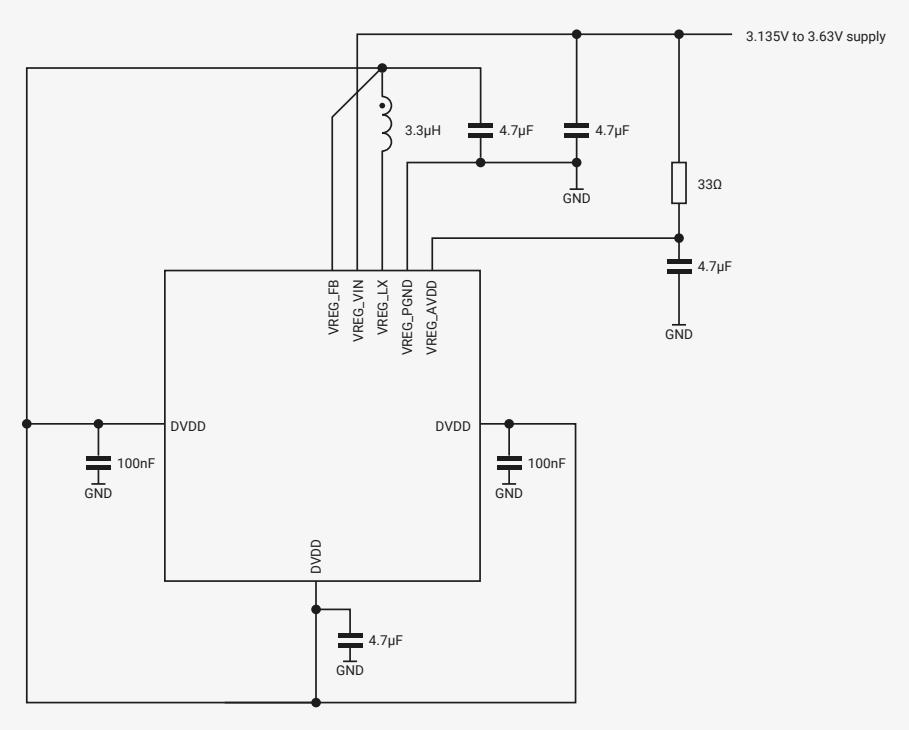
The diagram shows the internal structure of the core voltage regulator. It features a central block with pins labeled VREG_FB, VREG_VIN, VREG_LX, VREG_PGND, and VREG_AVDD. The VREG_VIN pin is connected to a 3.135V to 3.63V supply. The VREG_LX pin is connected to an inductor (3.3µH). The VREG_PGND pin is connected to ground. The VREG_AVDD pin is connected to a 33Ω resistor, which is then connected to ground. The VREG_FB pin is connected to a 100nF capacitor to ground. The output of the regulator is connected to a 4.7µF capacitor to ground. The output is also connected to a 3.135V to 3.63V supply. The output is also connected to a 4.7µF capacitor to ground. The output is also connected to a 3.135V to 3.63V supply. The output is also connected to a 4.7µF capacitor to ground.
Alternatively, to support input voltages above 3.63 V, VREG_VIN and VREG_AVDD can be powered separately. This is shown in Figure 20 .
Figure 20. Core voltage regulator with separate supplies
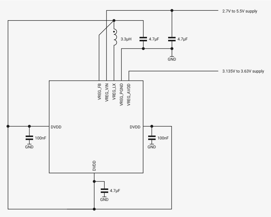
The diagram shows the internal structure of the core voltage regulator. It features a central block with pins labeled VREG_FB, VREG_VIN, VREG_LX, VREG_PGND, and VREG_AVDD. The VREG_VIN pin is connected to a 2.7V to 5.5V supply. The VREG_LX pin is connected to an inductor (3.3µH). The VREG_PGND pin is connected to ground. The VREG_AVDD pin is connected to a 3.135V to 3.63V supply. The VREG_FB pin is connected to a 100nF capacitor to ground. The output of the regulator is connected to a 4.7µF capacitor to ground. The output is also connected to a 3.135V to 3.63V supply. The output is also connected to a 4.7µF capacitor to ground.
If the digital core supply (DVDD) is powered from an external 1.1V supply, the on-chip regulator can be disabled and the application circuit simplified. Power must still be provided on the regulator's analogue supply ( VREG_AVDD ) and input supply ( VREG_VIN ) to power the chip's power-on reset and brown-out detection blocks. But the inductor can be omitted and only a single input capacitor is required. Connect VREG_FB directly to ground. This is shown in Figure 21 .
Figure 21. External core supply with on-chip regulator disabled.
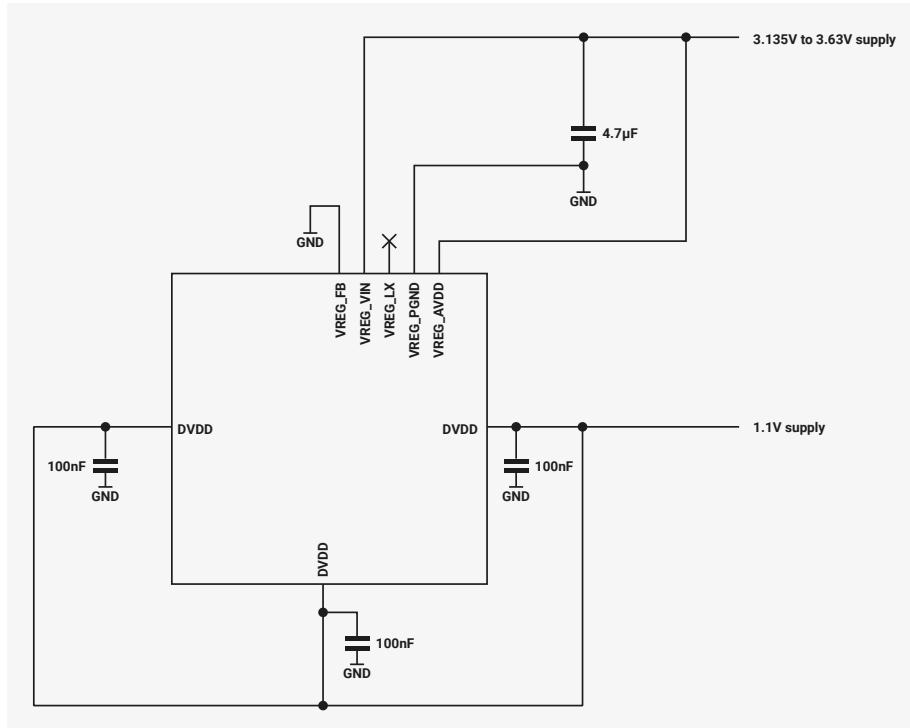
The diagram illustrates the external core supply configuration for the RP2350 when the on-chip regulator is disabled. A central chip is shown with several pins. A supply line labeled '3.135V to 3.63V supply' is connected to the VREG_VIN and VREG_AVDD pins. A 4.7µF capacitor is connected between this supply line and GND. Another supply line labeled '1.1V supply' is connected to the DVDD and VREG_PGND pins. There are three 100nF capacitors connected to GND: one between DVDD and GND on the left, one between DVDD and GND on the right, and one between DVDD and GND at the bottom. The chip pins are labeled VREG_FB, VREG_VIN, VREG_LX, VREG_PGND, and VREG_AVDD. A GND symbol is also shown near the top of the chip.
The on-chip regulator will still power on as soon as
VREG_VIN
and
VREG_AVDD
are available, but can be shut down under software control after the chip is out of reset. This is a safe mode of operation, though the regulator will consume approximately 400 µA until it's shut down. The regulator should be shut down by writing a 1 to the
VREG
register's HIZ field.
6.3.8. External components and PCB layout requirements
The most critical part of an RP2350 PCB layout is the core voltage regulator. This should be placed first on any board design and these guidelines must be strictly followed.
Figure 22. Regulator section of the Raspberry Pi Pico 2 schematic. The nets highlighted in bold show the high switching current paths
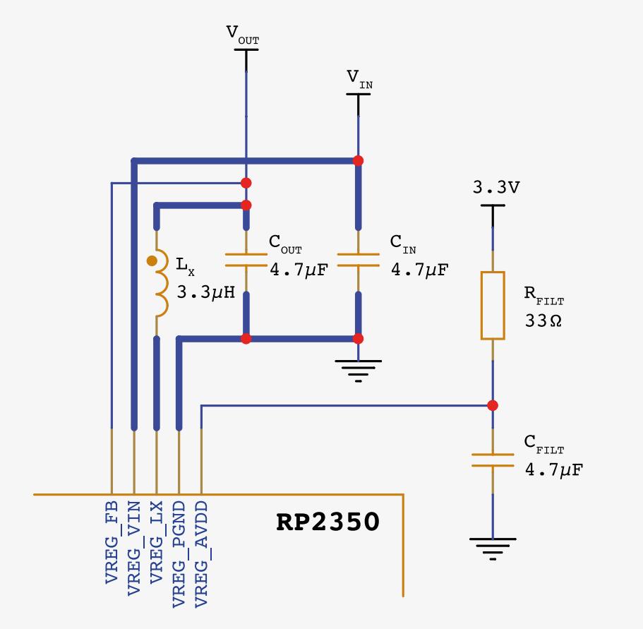
The diagram illustrates the regulator section of the RP2350, showing the internal circuitry and its connection to the Raspberry Pi Pico 2. The circuit is powered by a 3.3V input (V IN ) and provides a regulated output (V OUT ). The feedback path is connected to the VREG_FB pin. The input and output capacitors (C IN and C OUT ) are both 4.7μF. The output inductor (L x ) is 3.3μH. The feedback network consists of a resistor (R FILT ) and a capacitor (C FILT ), both 33Ω and 4.7μF respectively. The circuit is connected to the RP2350 pins VREG_FB, VREG_VIN, VREG_LX, VREG_PGND, and VREG_AVDD. The nets highlighted in bold show the high switching current paths.
Figure 23. Regulator section of the Raspberry Pi Pico 2 PCB layout showing the high current paths for each of the regulator's switching phases. The AOTA-B201610S3R3-101-T inductor's case size is 0806 (2016 metric), the resistor and capacitors are 0402 (1005 metric)
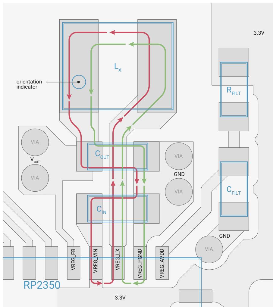
- For a multi-layer board (4 or more layers) please cut away any copper immediately underneath \( L_X/VREG\_LX \) node. For example, Figure 24 illustrates this.
- The GND via placement is critical.
- There must be a short-as-possible, low impedance GND path back to the Raspberry Pi Pico 2 QFN GND pad from the high-current GND at one single point (using 2 adjacent vias to reduce the impedance).
- \( C_{FILT} \) must also have a low impedance and short-as-possible path back to the QFN GND pad (don't share any GND vias with the \( C_{IN}/C_{OUT} \) high current GND).
- The VREG_FB pin should be fed from the output of \( C_{OUT} \) , avoiding routing directly underneath \( L_X \) .
- \(
C_{OUT}
\)
is critical for regulator performance and EMI. It must be placed between
\(
VREG\_VIN
\)
and
\(
VREG\_PGND
\)
as close to the pins as practically possible.
- In addition to \( C_{OUT} \) , for best performance we recommend a second 4.7 \( \mu \) F capacitor is used on the \( V_{OUT} \) net, located on the bottom edge of the package (DVDD pin 23 on the QFN-60). Don't place this near \( L_X/C_{OUT} \) .
Figure 24. Cut-out beneath \( L_X/VREG\_LX \) net on layer 2 of 4 (or more) layer PCBs
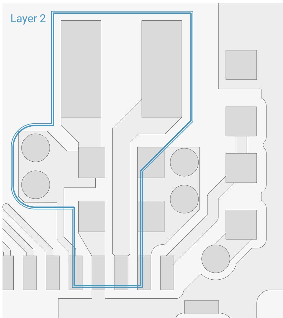
The diagram shows a top-down view of a PCB layout for Layer 2. A blue rectangular outline highlights a specific area where the copper must be cut out. This area is located beneath the LX/VREG_LX net. The layout includes various components represented by gray shapes: capacitors (circles), inductors (rectangles), and resistors (smaller rectangles). The cut-out is a rectangular area with rounded corners, following the general shape of the LX/VREG_LX net. The text 'Layer 2' is written in blue in the top left corner of the diagram area.
6.3.8.2. Component values
- \( C_{IN} \) should be at least 4.7 \( \mu \) F and have a maximum parasitic resistance of 50m \( \Omega \) .
- \( C_{OUT} \) must be 4.7 \( \mu \) F \( \pm \) 20% with a maximum parasitic resistance of 250m \( \Omega \) and a maximum inductance of 6nH.
- \( L_X \) must be fully shielded, 3.3 \( \mu \) H \( \pm \) 20% and with a maximum DC resistance of 250m \( \Omega \) . Saturation current should be at least 1.5A. The inductor must be marked for polarity (see Figure 25 ) and placed on the layout as indicated in Figure 23 . As discussed below, we recommend the AOTA-B201610S3R3-101-T .
6.3.8.3. Regulator sensitivities
The RP2350 regulator has a few sensitivities:
- • The
VREG_AVDDsupply is noise sensitive. - • Efficiency is quite sensitive to inductance roll-off with inductor current, so an inductor with low roll-off is required for best operation (generally the higher saturation current the better).
- • Even with nominally fully shielded inductors, leakage magnetic field coupling into the loop formed by the output
VREG_LXnode through the inductor and output capacitor ( \( C_{OUT} \) ) seems to affect the regulator control loop and output voltage. Field orientation (and hence inductor orientation) matters - the inductor has to be the right way around to make sure the regulator operates properly especially at higher output currents and for higher load transients. This necessitates an inductor with marked polarity.
To meet the above requirements, Raspberry Pi have worked with Abracon to create a custom 2.0×1.6mm 3.3μH polarity-marked inductor, part number
AOTA-B201610S3R3-101-T
(see
Figure 25
and
Figure 25
). These will be available in general distribution in time, but for now please contact Raspberry Pi to request samples / production volumes.
Raspberry Pi is still working with the regulator IP vendor to fully verify and qualify the regulator and custom inductor.
Figure 25.
AOTA-B201610S3R3-101-T
inductor with orientation marking, showing current and magnetic field directions
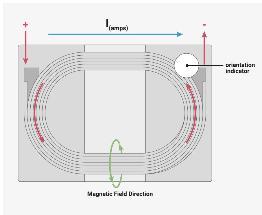
The diagram illustrates the internal structure of the inductor, which consists of multiple concentric elliptical turns. A blue arrow at the top indicates the current \( I \) (amps) flowing from the positive terminal (+) on the left to the negative terminal (-) on the right. Red arrows along the turns show the direction of current flow. A green circular arrow at the bottom indicates the 'Magnetic Field Direction'. A white circle on the right side is labeled 'orientation indicator'.
Figure 26. Dimensions of the AOTA-B201610S3R3-101-T inductor
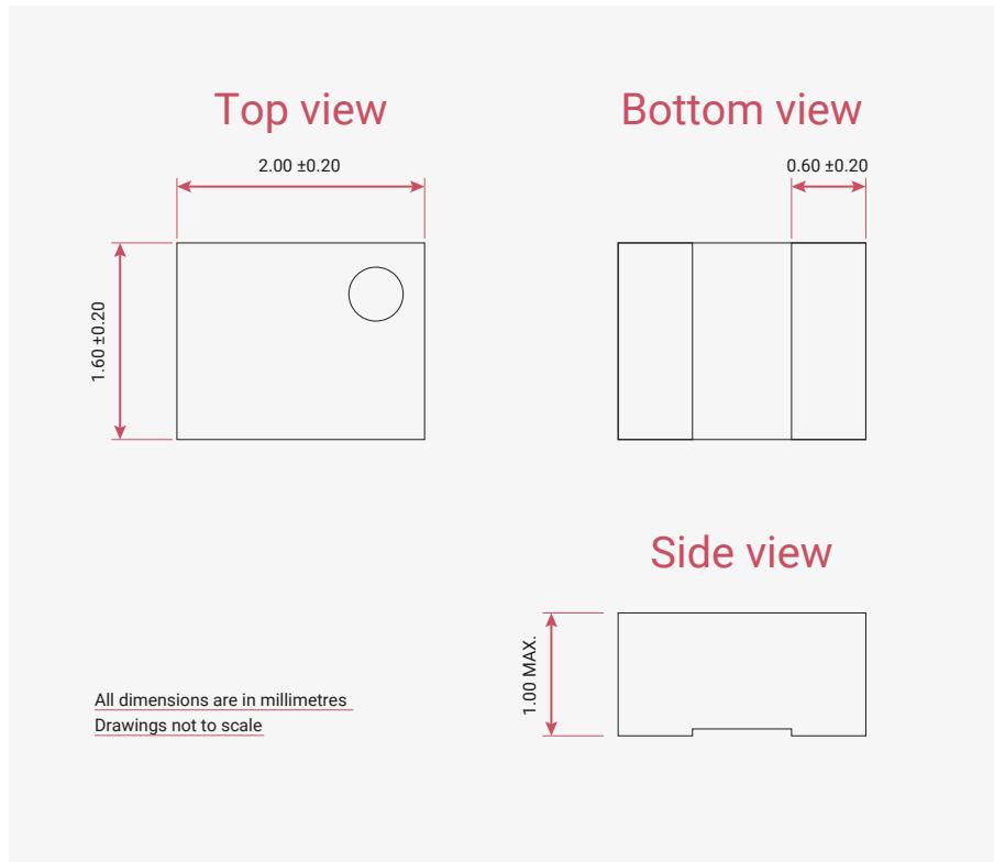
Top view
Bottom view
Side view
All dimensions are in millimetres
Drawings not to scale
6.3.9. List of registers
The voltage regulator shares a register address space with other power management subsystems in the always-on domain. This address space is referred to as POWMAN elsewhere in this document, and a complete list of POWMAN registers is provided in Section 6.4 . For reference information on POWMAN registers associated with the voltage regulator is repeated here.
The
POWMAN
registers start at a base address of
0x40100000
(defined as
POWMAN_BASE
in the SDK).
- • VREG_CTRL
- • VREG_STS
- • VREG
- • VREG_LP_ENTRY
- • VREG_LP_EXIT
6.4. Power management (POWMAN) registers
Password-protected
POWMAN
registers require a password (
0x5AFE
) to be written to the top 16 bits to enable the write operation. This protects against accidental writes that could crash the chip untraceably. Writes to protected registers that don't include the password are ignored, setting a flag in the
BADPASSWD
register. Reads from protected registers don't return the password, to protect against erroneous read-modify-write operations.
Protected registers obviously don't have writeable fields in the top 16 bits, however they may have read-only fields in that range.
All registers with address offsets up to and including
0x000000ac
are password protected. Therefore, the following writeable registers are unprotected and have 32-bit write access:
- • POWMAN_SCRATCH0 → POWMAN_SCRATCH7
- • POWMAN_BOOT0 → POWMAN_BOOT3
- • POWMAN_INTR
- • POWMAN_INTE
- • POWMAN_INTF
Table 477. List of POWMAN registers
| Offset | Name | Info |
|---|---|---|
| 0x00 | BADPASSWD | Indicates a bad password has been used |
| 0x04 | VREG_CTRL | Voltage Regulator Control |
| 0x08 | VREG_STS | Voltage Regulator Status |
| 0x0c | VREG | Voltage Regulator Settings |
| 0x10 | VREG_LP_ENTRY | Voltage Regulator Low Power Entry Settings |
| 0x14 | VREG_LP_EXIT | Voltage Regulator Low Power Exit Settings |
| 0x18 | BOD_CTRL | Brown-out Detection Control |
| 0x1c | BOD | Brown-out Detection Settings |
| 0x20 | BOD_LP_ENTRY | Brown-out Detection Low Power Entry Settings |
| 0x24 | BOD_LP_EXIT | Brown-out Detection Low Power Exit Settings |
| 0x28 | LPOSC | Low power oscillator control register. |
| 0x2c | CHIP_RESET | Chip reset control and status |
| 0x30 | WDSEL | Allows a watchdog reset to reset the internal state of powman in addition to the power-on state machine (PSM). Note that powman ignores watchdog resets that do not select at least the CLOCKS stage or earlier stages in the PSM. If using these bits, it's recommended to set PSM_WDSEL to all-ones in addition to the desired bits in this register. Failing to select CLOCKS or earlier will result in the POWMAN_WDSEL register having no effect. |
| 0x34 | SEQ_CFG | For configuration of the power sequencer Writes are ignored while POWMAN_STATE_CHANGING=1 |
| Offset | Name | Info |
|---|---|---|
| 0x38 | STATE | This register controls the power state of the 4 power domains. The current power state is indicated in POWMAN_STATE_CURRENT which is read-only. To change the state, write to POWMAN_STATE_REQ. The coding of POWMAN_STATE_CURRENT & POWMAN_STATE_REQ corresponds to the power states defined in the datasheet:
When POWMAN_STATE_REQ is written, the POWMAN_STATE_WAITING flag is set while the Power Manager determines what is required. If an invalid transition is requested the Power Manager will still register the request in POWMAN_STATE_REQ but will also set the POWMAN_BAD_REQ flag. It will then implement the power-up requests and ignore the power down requests. To do nothing would risk entering an unrecoverable lock-up state. Invalid requests are: any combination of power up and power down requests any request that results in swcore being powered and xip unpowered If the request is to power down the switched-core domain then POWMAN_STATE_WAITING stays active until the processors halt. During this time the POWMAN_STATE_REQ field can be re-written to change or cancel the request. When the power state transition begins the POWMAN_STATE_WAITING flag is cleared, the POWMAN_STATE_CHANGING flag is set and POWMAN register writes are ignored until the transition completes. |
| 0x3c | POW_FASTDIV | |
| 0x40 | POW_DELAY | power state machine delays |
| 0x44 | EXT_CTRL0 | Configures a gpio as a power mode aware control output |
| 0x48 | EXT_CTRL1 | Configures a gpio as a power mode aware control output |
| 0x4c | EXT_TIME_REF | Select a GPIO to use as a time reference, the source can be used to drive the low power clock at 32kHz, or to provide a 1ms tick to the timer, or provide a 1Hz tick to the timer. The tick selection is controlled by the POWMAN_TIMER register. |
| 0x50 | LPOSC_FREQ_KHZ_INT | Informs the AON Timer of the integer component of the clock frequency when running off the LPOSC. |
| 0x54 | LPOSC_FREQ_KHZ_FRAC | Informs the AON Timer of the fractional component of the clock frequency when running off the LPOSC. |
| 0x58 | XOSC_FREQ_KHZ_INT | Informs the AON Timer of the integer component of the clock frequency when running off the XOSC. |
| 0x5c | XOSC_FREQ_KHZ_FRAC | Informs the AON Timer of the fractional component of the clock frequency when running off the XOSC. |
| 0x60 | SET_TIME_63TO48 | |
| 0x64 | SET_TIME_47TO32 |
| Offset | Name | Info |
|---|---|---|
| 0x68 | SET_TIME_31TO16 | |
| 0x6c | SET_TIME_15TO0 | |
| 0x70 | READ_TIME_UPPER | |
| 0x74 | READ_TIME_LOWER | |
| 0x78 | ALARM_TIME_63TO48 | |
| 0x7c | ALARM_TIME_47TO32 | |
| 0x80 | ALARM_TIME_31TO16 | |
| 0x84 | ALARM_TIME_15TO0 | |
| 0x88 | TIMER | |
| 0x8c | PWRUP0 | 4 GPIO powerup events can be configured to wake the chip up from a low power state. The pwrups are level/edge sensitive and can be set to trigger on a high/rising or low/falling event The number of gpios available depends on the package option. An invalid selection will be ignored source = 0 selects gpio0 . . source = 47 selects gpio47 source = 48 selects qspi_ss source = 49 selects qspi_sd0 source = 50 selects qspi_sd1 source = 51 selects qspi_sd2 source = 52 selects qspi_sd3 source = 53 selects qspi_sclk level = 0 triggers the pwrup when the source is low level = 1 triggers the pwrup when the source is high |
| 0x90 | PWRUP1 | 4 GPIO powerup events can be configured to wake the chip up from a low power state. The pwrups are level/edge sensitive and can be set to trigger on a high/rising or low/falling event The number of gpios available depends on the package option. An invalid selection will be ignored source = 0 selects gpio0 . . source = 47 selects gpio47 source = 48 selects qspi_ss source = 49 selects qspi_sd0 source = 50 selects qspi_sd1 source = 51 selects qspi_sd2 source = 52 selects qspi_sd3 source = 53 selects qspi_sclk level = 0 triggers the pwrup when the source is low level = 1 triggers the pwrup when the source is high |
| Offset | Name | Info |
|---|---|---|
| 0x94 | PWRUP2 | 4 GPIO powerup events can be configured to wake the chip up from a low power state. The pwrups are level/edge sensitive and can be set to trigger on a high/rising or low/falling event The number of gpios available depends on the package option. An invalid selection will be ignored source = 0 selects gpio0 . . source = 47 selects gpio47 source = 48 selects qspi_ss source = 49 selects qspi_sd0 source = 50 selects qspi_sd1 source = 51 selects qspi_sd2 source = 52 selects qspi_sd3 source = 53 selects qspi_sclk level = 0 triggers the pwrup when the source is low level = 1 triggers the pwrup when the source is high |
| 0x98 | PWRUP3 | 4 GPIO powerup events can be configured to wake the chip up from a low power state. The pwrups are level/edge sensitive and can be set to trigger on a high/rising or low/falling event The number of gpios available depends on the package option. An invalid selection will be ignored source = 0 selects gpio0 . . source = 47 selects gpio47 source = 48 selects qspi_ss source = 49 selects qspi_sd0 source = 50 selects qspi_sd1 source = 51 selects qspi_sd2 source = 52 selects qspi_sd3 source = 53 selects qspi_sclk level = 0 triggers the pwrup when the source is low level = 1 triggers the pwrup when the source is high |
| 0x9c | CURRENT_PWRUP_REQ | Indicates current powerup request state pwrup events can be cleared by removing the enable from the pwrup register. The alarm pwrup req can be cleared by clearing timer.alarm_enab 0 = chip reset, for the source of the last reset see POWMAN_CHIP_RESET 1 = pwrup0 2 = pwrup1 3 = pwrup2 4 = pwrup3 5 = coresight_pwrup 6 = alarm_pwrup |
| Offset | Name | Info |
|---|---|---|
| 0xa0 | LAST_SWCORE_PWRUP | Indicates which pwrup source triggered the last switched-core power up 0 = chip reset, for the source of the last reset see POWMAN_CHIP_RESET 1 = pwrup0 2 = pwrup1 3 = pwrup2 4 = pwrup3 5 = coresight_pwrup 6 = alarm_pwrup |
| 0xa4 | DBG_PWRCFG | |
| 0xa8 | BOOTDIS | Tell the bootrom to ignore the BOOT0..3 registers following the next RSM reset (e.g. the next core power down/up). If an early boot stage has soft-locked some OTP pages in order to protect their contents from later stages, there is a risk that Secure code running at a later stage can unlock the pages by powering the core up and down. This register can be used to ensure that the bootloader runs as normal on the next power up, preventing Secure code at a later stage from accessing OTP in its unlocked state. Should be used in conjunction with the OTP BOOTDIS register. |
| 0xac | DBGCONFIG | |
| 0xb0 | SCRATCH0 | Scratch register. Information persists in low power mode |
| 0xb4 | SCRATCH1 | Scratch register. Information persists in low power mode |
| 0xb8 | SCRATCH2 | Scratch register. Information persists in low power mode |
| 0xbc | SCRATCH3 | Scratch register. Information persists in low power mode |
| 0xc0 | SCRATCH4 | Scratch register. Information persists in low power mode |
| 0xc4 | SCRATCH5 | Scratch register. Information persists in low power mode |
| 0xc8 | SCRATCH6 | Scratch register. Information persists in low power mode |
| 0xcc | SCRATCH7 | Scratch register. Information persists in low power mode |
| 0xd0 | BOOT0 | Scratch register. Information persists in low power mode |
| 0xd4 | BOOT1 | Scratch register. Information persists in low power mode |
| 0xd8 | BOOT2 | Scratch register. Information persists in low power mode |
| 0xdc | BOOT3 | Scratch register. Information persists in low power mode |
| 0xe0 | INTR | Raw Interrupts |
| 0xe4 | INTE | Interrupt Enable |
| 0xe8 | INTF | Interrupt Force |
| 0xec | INTS | Interrupt status after masking & forcing |
POWMAN: BADPASSWD Register
Offset: 0x00
Table 478.
BADPASSWD Register
| Bits 14:10 9:5 4:0 Bits | Description SHIFT Description | MASK_MSB : The most-significant bit allowed to pass by the mask (inclusive) MASK_LSB : The least-significant bit allowed to pass by the mask (inclusive) : Right-rotate applied to accumulator before masking. By appropriately | Type RW RW RW Type | Reset 0x00 0x00 0x00 Reset |
|---|---|---|---|---|
| 31:1 | Reserved. | - | - | |
| 0 | Indicates a bad password has been used | WC | 0x0 | |
| Table 479. Bits | Description | Type | Reset | |
| VREG_CTRL Register 31:16 | Reserved. | - | - | |
| 15 | RST_N 0 - reset | : returns the regulator to its startup settings | RW | 0x1 |
| 14 | Reserved. | - | - | |
| 13 | UNLOCK | : unlocks the VREG control interface after power up 0 - Locked (default) | RW | 0x0 |
| 12 | ISOLATE | It cannot be relocked when it is unlocked. : isolates the VREG control interface 0 - not isolated (default) | RW | 0x0 |
| 11:9 | 1 - isolated Reserved. | - | - | |
| 8 | DISABLE_VOLTAGE_LIMIT | : 0=not disabled, 1=enabled | RW | 0x0 |
| 7 | Reserved. | - | - | |
| 6:4 | HT_TH | : high temperature protection threshold | RW | 0x5 |
| 3:2 | 111 - 150C Reserved. | - | - | |
| 1:0 | RESERVED | : write 0 to this field | RW | 0x0 |
POWMAN: VREG_CTRL Register
Offset: 0x04
Description
Voltage Regulator Control
Table 479.
VREG_CTRL Register
POWMAN: VREG_STS Register
Offset: 0x08
Description
Voltage Regulator Status
Table 480. VREG_STS
Register
| Bits | Description | Type | Reset |
|---|---|---|---|
| 31:5 | Reserved. | - | - |
| 4 | VOUT_OK
: output regulation status 0=not in regulation, 1=in regulation | RO | 0x0 |
| 3:1 | Reserved. | - | - |
| 0 | STARTUP
: startup status 0=startup complete, 1=starting up | RO | 0x0 |
POWMAN: VREG Register
Offset: 0x0c
Description
Voltage Regulator Settings
Table 481. VREG Register
| Bits | Description | Type | Reset |
|---|---|---|---|
| 31:16 | Reserved. | - | - |
| 15 | UPDATE_IN_PROGRESS
: regulator state is being updated writes to the vreg register will be ignored when this field is set | RO | 0x0 |
| 14:9 | Reserved. | - | - |
| Bits | Description | Type | Reset |
|---|---|---|---|
| 8:4 | VSEL
: output voltage select the regulator output voltage is limited to 1.3V unless the voltage limit is disabled using the disable_voltage_limit field in the vreg_ctrl register 00000 - 0.55V 00001 - 0.60V 00010 - 0.65V 00011 - 0.70V 00100 - 0.75V 00101 - 0.80V 00110 - 0.85V 00111 - 0.90V 01000 - 0.95V 01001 - 1.00V 01010 - 1.05V 01011 - 1.10V (default) 01100 - 1.15V 01101 - 1.20V 01110 - 1.25V 01111 - 1.30V 10000 - 1.35V 10001 - 1.40V 10010 - 1.50V 10011 - 1.60V 10100 - 1.65V 10101 - 1.70V 10110 - 1.80V 10111 - 1.90V 11000 - 2.00V 11001 - 2.35V 11010 - 2.50V 11011 - 2.65V 11100 - 2.80V 11101 - 3.00V 11110 - 3.15V 11111 - 3.30V | RW | 0x0b |
| 3 | Reserved. | - | - |
| 2 | RESERVED : write 0 to this field | RW | 0x0 |
| 1 | HIZ
: high impedance mode select 0=not in high impedance mode, 1=in high impedance mode | RW | 0x0 |
| 0 | Reserved. | - | - |
POWMAN: VREG_LP_ENTRY Register
Offset: 0x10
Description
Voltage Regulator Low Power Entry Settings
Table 482.
VREG_LP_ENTRY
Register
| Bits | Description | Type | Reset |
|---|---|---|---|
| 31:9 | Reserved. | - | - |
| Bits | Description | Type | Reset |
|---|---|---|---|
| 8:4 | VSEL
: output voltage select the regulator output voltage is limited to 1.3V unless the voltage limit is disabled using the disable_voltage_limit field in the vreg_ctrl register 00000 - 0.55V 00001 - 0.60V 00010 - 0.65V 00011 - 0.70V 00100 - 0.75V 00101 - 0.80V 00110 - 0.85V 00111 - 0.90V 01000 - 0.95V 01001 - 1.00V 01010 - 1.05V 01011 - 1.10V (default) 01100 - 1.15V 01101 - 1.20V 01110 - 1.25V 01111 - 1.30V 10000 - 1.35V 10001 - 1.40V 10010 - 1.50V 10011 - 1.60V 10100 - 1.65V 10101 - 1.70V 10110 - 1.80V 10111 - 1.90V 11000 - 2.00V 11001 - 2.35V 11010 - 2.50V 11011 - 2.65V 11100 - 2.80V 11101 - 3.00V 11110 - 3.15V 11111 - 3.30V | RW | 0x0b |
| 3 | Reserved. | - | - |
| 2 | MODE
: selects either normal (switching) mode or low power (linear) mode low power mode can only be selected for output voltages up to 1.3V 0 = normal mode (switching) 1 = low power mode (linear) | RW | 0x1 |
| 1 | HIZ
: high impedance mode select 0=not in high impedance mode, 1=in high impedance mode | RW | 0x0 |
| 0 | Reserved. | - | - |
POWMAN: VREG_LP_EXIT Register
Offset: 0x14
Description
Voltage Regulator Low Power Exit Settings
Table 483.
VREG_LP_EXIT
Register
| Bits | Description | Type | Reset |
|---|---|---|---|
| 31:9 | Reserved. | - | - |
| 8:4 | VSEL
: output voltage select the regulator output voltage is limited to 1.3V unless the voltage limit is disabled using the disable_voltage_limit field in the vreg_ctrl register 00000 - 0.55V 00001 - 0.60V 00010 - 0.65V 00011 - 0.70V 00100 - 0.75V 00101 - 0.80V 00110 - 0.85V 00111 - 0.90V 01000 - 0.95V 01001 - 1.00V 01010 - 1.05V 01011 - 1.10V (default) 01100 - 1.15V 01101 - 1.20V 01110 - 1.25V 01111 - 1.30V 10000 - 1.35V 10001 - 1.40V 10010 - 1.50V 10011 - 1.60V 10100 - 1.65V 10101 - 1.70V 10110 - 1.80V 10111 - 1.90V 11000 - 2.00V 11001 - 2.35V 11010 - 2.50V 11011 - 2.65V 11100 - 2.80V 11101 - 3.00V 11110 - 3.15V 11111 - 3.30V | RW | 0x0b |
| 3 | Reserved. | - | - |
| 2 | MODE
: selects either normal (switching) mode or low power (linear) mode low power mode can only be selected for output voltages up to 1.3V 0 = normal mode (switching) 1 = low power mode (linear) | RW | 0x0 |
| 1 | HIZ
: high impedance mode select 0=not in high impedance mode, 1=in high impedance mode | RW | 0x0 |
| 0 | Reserved. | - | - |
POWMAN: BOD_CTRL Register
Offset: 0x18
Description
Brown-out Detection Control
Table 484. BOD_CTRL Register
| Bits | Description | Type | Reset |
|---|---|---|---|
| 31:13 | Reserved. | - | - |
| 12 | ISOLATE
: isolates the brown-out detection control interface 0 - not isolated (default) 1 - isolated | RW | 0x0 |
| 11:0 | Reserved. | - | - |
POWMAN: BOD Register
Offset: 0x1c
Description
Brown-out Detection Settings
Table 485. BOD Register
| Bits | Description | Type | Reset |
|---|---|---|---|
| 31:9 | Reserved. | - | - |
| 8:4 | VSEL
: threshold select 00000 - 0.473V 00001 - 0.516V 00010 - 0.559V 00011 - 0.602V 00100 - 0.645VS 00101 - 0.688V 00110 - 0.731V 00111 - 0.774V 01000 - 0.817V 01001 - 0.860V (default) 01010 - 0.903V 01011 - 0.946V 01100 - 0.989V 01101 - 1.032V 01110 - 1.075V 01111 - 1.118V 10000 - 1.161 10001 - 1.204V | RW | 0x0b |
| 3:1 | Reserved. | - | - |
| 0 | EN
: enable brown-out detection 0=not enabled, 1=enabled | RW | 0x1 |
POWMAN: BOD_LP_ENTRY Register
Offset: 0x20
Description
Brown-out Detection Low Power Entry Settings
Table 486. BOD_LP_ENTRY Register
| Bits | Description | Type | Reset |
|---|---|---|---|
| 31:9 | Reserved. | - | - |
| Bits | Description | Type | Reset |
|---|---|---|---|
| 8:4 | VSEL
: threshold select 00000 - 0.473V 00001 - 0.516V 00010 - 0.559V 00011 - 0.602V 00100 - 0.645VS 00101 - 0.688V 00110 - 0.731V 00111 - 0.774V 01000 - 0.817V 01001 - 0.860V (default) 01010 - 0.903V 01011 - 0.946V 01100 - 0.989V 01101 - 1.032V 01110 - 1.075V 01111 - 1.118V 10000 - 1.161 10001 - 1.204V | RW | 0x0b |
| 3:1 | Reserved. | - | - |
| 0 | EN
: enable brown-out detection 0=not enabled, 1=enabled | RW | 0x0 |
POWMAN: BOD_LP_EXIT Register
Offset: 0x24
Description
Brown-out Detection Low Power Exit Settings
Table 487.
BOD_LP_EXIT Register
| Bits | Description | Type | Reset |
|---|---|---|---|
| 31:9 | Reserved. | - | - |
| 8:4 | VSEL
: threshold select 00000 - 0.473V 00001 - 0.516V 00010 - 0.559V 00011 - 0.602V 00100 - 0.645VS 00101 - 0.688V 00110 - 0.731V 00111 - 0.774V 01000 - 0.817V 01001 - 0.860V (default) 01010 - 0.903V 01011 - 0.946V 01100 - 0.989V 01101 - 1.032V 01110 - 1.075V 01111 - 1.118V 10000 - 1.161 10001 - 1.204V | RW | 0x0b |
| 3:1 | Reserved. | - | - |
| Bits | Description | Type | Reset |
|---|---|---|---|
| 0 | EN
: enable brown-out detection 0=not enabled, 1=enabled | RW | 0x1 |
POWMAN: LPOSC Register
Offset: 0x28
Description
Low power oscillator control register.
Table 488. LPOSC Register
| Bits | Description | Type | Reset |
|---|---|---|---|
| 31:10 | Reserved. | - | - |
| 9:4 | TRIM : Frequency trim - the trim step is typically 1% of the reset frequency, but can be up to 3% | RW | 0x20 |
| 3:2 | Reserved. | - | - |
| 1:0 | MODE : This feature has been removed | RW | 0x3 |
POWMAN: CHIP_RESET Register
Offset: 0x2c
Description
Chip reset control and status
Table 489. CHIP_RESET Register
| Bits | Description | Type | Reset |
|---|---|---|---|
| 31:29 | Reserved. | - | - |
| 28 | HAD_WATCHDOG_RESET_PSM
: Last reset was a watchdog timeout which was configured to reset the power-on state machine This resets: double_tap flag no DP no RPAP no rescue_flag no timer no powman no swcore no psm yes and does not change the power state | RO | 0x0 |
| 27 | HAD_HZD_SYS_RESET_REQ
: Last reset was a system reset from the hazard debugger This resets: double_tap flag no DP no RPAP no rescue_flag no timer no powman no swcore no psm yes and does not change the power state | RO | 0x0 |
| Bits | Description | Type | Reset |
|---|---|---|---|
| 26 | HAD_GLITCH_DETECT:
Last reset was due to a power supply glitch This resets: double_tap flag no DP no RPAP no rescue_flag no timer no powman no swcore no psm yes and does not change the power state | RO | 0x0 |
| 25 | HAD_SWCORE_PD:
Last reset was a switched core powerdown This resets: double_tap flag no DP no RPAP no rescue_flag no timer no powman no swcore yes psm yes then starts the power sequencer | RO | 0x0 |
| 24 | HAD_WATCHDOG_RESET_SWCORE:
Last reset was a watchdog timeout which was configured to reset the switched-core This resets: double_tap flag no DP no RPAP no rescue_flag no timer no powman no swcore yes psm yes then starts the power sequencer | RO | 0x0 |
| 23 | HAD_WATCHDOG_RESET_POWMAN:
Last reset was a watchdog timeout which was configured to reset the power manager This resets: double_tap flag no DP no RPAP no rescue_flag no timer yes powman yes swcore yes psm yes then starts the power sequencer | RO | 0x0 |
| Bits | Description | Type | Reset |
|---|---|---|---|
| 22 | HAD_WATCHDOG_RESET_POWMAN_ASYNC:
Last reset was a watchdog timeout which was configured to reset the power manager asynchronously This resets: double_tap flag no DP no RPAP no rescue_flag no timer yes powman yes swcore yes psm yes then starts the power sequencer | RO | 0x0 |
| 21 | HAD_RESCUE:
Last reset was a rescue reset from the debugger This resets: double_tap flag no DP no RPAP no rescue_flag no, it sets this flag timer yes powman yes swcore yes psm yes then starts the power sequencer | RO | 0x0 |
| 20 | Reserved. | - | - |
| 19 | HAD_DP_RESET_REQ:
Last reset was an reset request from the arm debugger This resets: double_tap flag no DP no RPAP no rescue_flag yes timer yes powman yes swcore yes psm yes then starts the power sequencer | RO | 0x0 |
| 18 | HAD_RUN_LOW:
Last reset was from the RUN pin This resets: double_tap flag no DP yes RPAP yes rescue_flag yes timer yes powman yes swcore yes psm yes then starts the power sequencer | RO | 0x0 |
| Bits | Description | Type | Reset |
|---|---|---|---|
| 17 | HAD_BOR:
Last reset was from the brown-out detection block This resets: double_tap flag yes DP yes RPAP yes rescue_flag yes timer yes powman yes swcore yes psm yes then starts the power sequencer | RO | 0x0 |
| 16 | HAD_POR:
Last reset was from the power-on reset This resets: double_tap flag yes DP yes RPAP yes rescue_flag yes timer yes powman yes swcore yes psm yes then starts the power sequencer | RO | 0x0 |
| 15:5 | Reserved. | - | - |
| 4 | RESCUE_FLAG:
This is set by a rescue reset from the RP-AP. Its purpose is to halt before the bootrom before booting from flash in order to recover from a boot lock-up. The debugger can then attach once the bootrom has been halted and flash some working code that does not lock up. | WC | 0x0 |
| 3:1 | Reserved. | - | - |
| 0 | DOUBLE_TAP: This flag is set by double-tapping RUN. It tells bootcode to go into the bootloader. | RW | 0x0 |
POWMAN: WDSEL Register
Offset: 0x30
Description
Allows a watchdog reset to reset the internal state of powman in addition to the power-on state machine (PSM).
Note that powman ignores watchdog resets that do not select at least the CLOCKS stage or earlier stages in the PSM. If using these bits, it's recommended to set PSM_WDSEL to all-ones in addition to the desired bits in this register. Failing to select CLOCKS or earlier will result in the POWMAN_WDSEL register having no effect.
Table 490. WDSEL Register
| Bits | Description | Type | Reset |
|---|---|---|---|
| 31:13 | Reserved. | - | - |
| 12 | RESET_PSM:
If set to 1, a watchdog reset will run the full power-on state machine (PSM) sequence From a user perspective it is the same as setting RSM_WDSEL_PROC_COLD From a hardware debug perspective it has the same effect as a reset from a glitch detector | RW | 0x0 |
| 11:9 | Reserved. | - | - |
| Bits | Description | Type | Reset |
|---|---|---|---|
| 8 | RESET_SWCORE:
If set to 1, a watchdog reset will reset the switched core power domain and run the full power-on state machine (PSM) sequence From a user perspective it is the same as setting RSM_WDSEL_PROC_COLD From a hardware debug perspective it has the same effect as a power-on reset for the switched core power domain | RW | 0x0 |
| 7:5 | Reserved. | - | - |
| 4 | RESET_POWMAN:
If set to 1, a watchdog reset will restore powman defaults, reset the timer, reset the switched core power domain and run the full power-on state machine (PSM) sequence This relies on clk_ref running. Use reset_powman_async if that may not be true | RW | 0x0 |
| 3:1 | Reserved. | - | - |
| 0 | RESET_POWMAN_ASYNC:
If set to 1, a watchdog reset will restore powman defaults, reset the timer, reset the switched core domain and run the full power-on state machine (PSM) sequence This does not rely on clk_ref running | RW | 0x0 |
POWMAN: SEQ_CFG Register
Offset: 0x34
Description
For configuration of the power sequencer
Writes are ignored while POWMAN_STATE_CHANGING=1
Table 491. SEQ_CFG Register
| Bits | Description | Type | Reset |
|---|---|---|---|
| 31:21 | Reserved. | - | - |
| 20 | USING_FAST_POWCK:
0 indicates the POWMAN clock is running from the low power oscillator (32kHz) 1 indicates the POWMAN clock is running from the reference clock (2-50MHz) | RO | 0x1 |
| 19:18 | Reserved. | - | - |
| 17 | USING_BOD_LP:
Indicates the brown-out detector (BOD) mode 0 = BOD high power mode which is the default 1 = BOD low power mode | RO | 0x0 |
| 16 | USING_VREG_LP:
Indicates the voltage regulator (VREG) mode 0 = VREG high power mode which is the default 1 = VREG low power mode | RO | 0x0 |
| 15:13 | Reserved. | - | - |
| 12 | USE_FAST_POWCK:
selects the reference clock (clk_ref) as the source of the POWMAN clock when switched-core is powered. The POWMAN clock always switches to the slow clock (lposc) when switched-core is powered down because the fast clock stops running. 0 always run the POWMAN clock from the slow clock (lposc) 1 run the POWMAN clock from the fast clock when available This setting takes effect when a power up sequence is next run | RW | 0x1 |
| 11:9 | Reserved. | - | - |
| Bits | Description | Type | Reset |
|---|---|---|---|
| 8 | RUN_LPOSC_IN_LP
: Set to 0 to stop the low power osc when the switched-core is powered down, which is unwise if using it to clock the timer This setting takes effect when the swcore is next powered down | RW | 0x1 |
| 7 | USE_BOD_HP
: Set to 0 to prevent automatic switching to bod high power mode when switched-core is powered up This setting takes effect when the swcore is next powered up | RW | 0x1 |
| 6 | USE_BOD_LP
: Set to 0 to prevent automatic switching to bod low power mode when switched-core is powered down This setting takes effect when the swcore is next powered down | RW | 0x1 |
| 5 | USE_VREG_HP
: Set to 0 to prevent automatic switching to vreg high power mode when switched-core is powered up This setting takes effect when the swcore is next powered up | RW | 0x1 |
| 4 | USE_VREG_LP
: Set to 0 to prevent automatic switching to vreg low power mode when switched-core is powered down This setting takes effect when the swcore is next powered down | RW | 0x1 |
| 3:2 | Reserved. | - | - |
| 1 | HW_PWRUP_SRAM0
: Specifies the power state of SRAM0 when powering up swcore from a low power state (P1.xxx) to a high power state (P0.0xx). 0=power-up 1=no change | RW | 0x0 |
| 0 | HW_PWRUP_SRAM1
: Specifies the power state of SRAM1 when powering up swcore from a low power state (P1.xxx) to a high power state (P0.0xx). 0=power-up 1=no change | RW | 0x0 |
POWMAN: STATE Register
Offset: 0x38
Description
This register controls the power state of the 4 power domains.
The current power state is indicated in POWMAN_STATE_CURRENT which is read-only.
To change the state, write to POWMAN_STATE_REQ.
The coding of POWMAN_STATE_CURRENT & POWMAN_STATE_REQ corresponds to the power states defined in the datasheet:
bit 3 = SWCORE
bit 2 = XIP cache
bit 1 = SRAM0
bit 0 = SRAM1
0 = powered up
1 = powered down
When POWMAN_STATE_REQ is written, the POWMAN_STATE_WAITING flag is set while the Power Manager determines what is required. If an invalid transition is requested the Power Manager will still register the request in POWMAN_STATE_REQ but will also set the POWMAN_BAD_REQ flag. It will then implement the power-up requests and ignore the power down requests. To do nothing would risk entering an unrecoverable lock-up state. Invalid requests are: any combination of power up and power down requests any request that results in swcore being powered and xip unpowered If the request is to power down the switched-core domain then POWMAN_STATE_WAITING stays active until the processors halt. During this time the POWMAN_STATE_REQ field can be re-written to change or cancel the request. When the power state transition begins the POWMAN_STATE_WAITING_flag is cleared, the POWMAN_STATE_CHANGING flag is set and POWMAN register writes are ignored until the transition completes.
Table 492. STATE Register
| Bits 14:10 9:5 4:0 Bits | Description SHIFT Description | MASK_MSB : The most-significant bit allowed to pass by the mask (inclusive) MASK_LSB : The least-significant bit allowed to pass by the mask (inclusive) : Right-rotate applied to accumulator before masking. By appropriately | Type RW RW RW Type | Reset 0x00 0x00 0x00 Reset |
|---|---|---|---|---|
| 31:14 | Reserved. | - | - | |
| 13 | CHANGING | : Indicates a power state change is in progress | RO | 0x0 |
| 12 | WAITING | : Indicates the power manager has received a state change request and is waiting for other actions to complete before executing it | RO | 0x0 |
| 11 | BAD_HW_REQ | : Invalid hardware initiated state request, power up requests actioned, power down requests ignored | RO | 0x0 |
| 10 | BAD_SW_REQ | : Invalid software initiated state request ignored | RO | 0x0 |
| 9 | PWRUP_WHILE_WAITING | : Indicates that a power state change request was ignored because of a pending power state change request | WC | 0x0 |
| 8 | REQ_IGNORED | : Indicates that a software state change request was ignored because it clashed with an ongoing hardware or debugger request | WC | 0x0 |
| 7:4 | REQ : This is written by software or hardware to request a new power state | RW | 0x0 | |
| 3:0 | CURRENT POWMAN: | : Indicates the current power state POW_FASTDIV Register | RO | 0xf |
| Table 493. Offset Bits POW_FASTDIV | : 0x3c Description | Type | Reset | |
| Register 31:11 | Reserved. | - | - | |
| 10:0 | divides the POWMAN clock to provide a tick for the delay module and state machines | RW | 0x040 | |
| Table 494. Bits POW_DELAY Register | Description | Type | Reset | |
| 31:16 | Reserved. | - | - | |
| 15:8 | SRAM_STEP steps | : timing between the sram0 and sram1 power state machine | RW | 0x20 |
| 7:4 | XIP_STEP | : timing between the xip power state machine steps measured in units of the lposc period, 0 gives a delay of 1 unit | RW | 0x1 |
| 3:0 | SWCORE_STEP | : timing between the swcore power state machine steps measured in units of the lposc period, 0 gives a delay of 1 unit | RW | 0x1 |
POWMAN: POW_FASTDIV Register
Offset: 0x3c
Table 493. POW_FASTDIV Register
POWMAN: POW_DELAY Register
Offset: 0x40
Description
power state machine delays
Table 494. POW_DELAY Register
POWMAN: EXT_CTRL0 Register
Offset: 0x44
Description
Configures a gpio as a power mode aware control output
Table 495. EXT_CTRL0 Register
| Bits | Description | Type | Reset |
|---|---|---|---|
| 31:15 | Reserved. | - | - |
| 14 | LP_EXIT_STATE : output level when exiting the low power state | RW | 0x0 |
| 13 | LP_ENTRY_STATE : output level when entering the low power state | RW | 0x0 |
| 12 | INIT_STATE | RW | 0x0 |
| 11:9 | Reserved. | - | - |
| 8 | INIT | RW | 0x0 |
| 7:6 | Reserved. | - | - |
| 5:0 | GPIO_SELECT : selects from gpio 0 →30 set to 31 to disable this feature | RW | 0x3f |
| Table 496. EXT_CTRL1 Bits | Configures a gpio as a power mode aware control output Description | Type | Reset |
| Register 31:15 | Reserved. | - | - |
| 14 | LP_EXIT_STATE : output level when exiting the low power state | RW | 0x0 |
| 13 | LP_ENTRY_STATE : output level when entering the low power state | RW | 0x0 |
| 12 | INIT_STATE | RW | 0x0 |
| 11:9 | Reserved. | - | - |
| 8 | INIT | RW | 0x0 |
| 7:6 | Reserved. | - | - |
| 5:0 | GPIO_SELECT : selects from gpio 0 →30 set to 31 to disable this feature | RW | 0x3f |
| Table 497. Bits | POWMAN_TIMER register. Description | Type | Reset |
| EXT_TIME_REF Register 31:5 | Reserved. | - | - |
| 4 | DRIVE_LPCK : Use the selected GPIO to drive the 32kHz low power clock, in place of LPOSC. This field must only be written when | RW | 0x0 |
| 3:2 | POWMAN_TIMER_RUN=0 Reserved. | - | - |
POWMAN: EXT_CTRL1 Register
Offset: 0x48
Description
Configures a gpio as a power mode aware control output
Table 496. EXT_CTRL1 Register
POWMAN: EXT_TIME_REF Register
Offset: 0x4c
Description
Select a GPIO to use as a time reference, the source can be used to drive the low power clock at 32kHz, or to provide a 1ms tick to the timer, or provide a 1Hz tick to the timer. The tick selection is controlled by the POWMAN_TIMER register.
Table 497. EXT_TIME_REF Register
| Bits | Description | Type | Reset |
|---|---|---|---|
| 1:0 | SOURCE_SEL:
0 → gpio12 1 → gpio20 2 → gpio14 3 → gpio22 | RW | 0x0 |
| Enumerated values: | |||
| 0x0 → GPIO12 | |||
| 0x1 → GPIO20 | |||
| 0x2 → GPIO14 | |||
| 0x3 → GPIO22 |
POWMAN: LPOSC_FREQ_KHZ_INT Register
Offset: 0x50
Description
Inform the AON Timer of the integer component of the clock frequency when running off the LPOSC.
Table 498.
LPOSC_FREQ_KHZ_INT
Register
| Bits | Description | Type | Reset |
|---|---|---|---|
| 31:6 | Reserved. | - | - |
| 5:0 | Integer component of the LPOSC or GPIO clock source frequency in kHz. Default = 32 This field must only be written when POWMAN_TIMER_RUN=0 or POWMAN_TIMER_USING_XOSC=1 | RW | 0x20 |
POWMAN: LPOSC_FREQ_KHZ_FRAC Register
Offset: 0x54
Description
Inform the AON Timer of the fractional component of the clock frequency when running off the LPOSC.
Table 499.
LPOSC_FREQ_KHZ_FRAC
Register
| Bits | Description | Type | Reset |
|---|---|---|---|
| 31:16 | Reserved. | - | - |
| 15:0 | Fractional component of the LPOSC or GPIO clock source frequency in kHz. Default = 0.768 This field must only be written when POWMAN_TIMER_RUN=0 or POWMAN_TIMER_USING_XOSC=1 | RW | 0xc49c |
POWMAN: XOSC_FREQ_KHZ_INT Register
Offset: 0x58
Description
Inform the AON Timer of the integer component of the clock frequency when running off the XOSC.
Table 500.
XOSC_FREQ_KHZ_INT
Register
| Bits | Description | Type | Reset |
|---|---|---|---|
| 31:16 | Reserved. | - | - |
| 15:0 | Integer component of the XOSC frequency in kHz. Default = 12000 Must be >1 This field must only be written when POWMAN_TIMER_RUN=0 or POWMAN_TIMER_USING_XOSC=0 | RW | 0x2ee0 |
POWMAN: XOSC_FREQ_KHZ_FRAC Register
Offset: 0x5c
Description
Informs the AON Timer of the fractional component of the clock frequency when running off the XOSC.
Table 501.
XOSC_FREQ_KHZ_FRA
C Register
| Bits | Description | Type | Reset |
|---|---|---|---|
| 31:16 | Reserved. | - | - |
| 15:0 | Fractional component of the XOSC frequency in kHz. This field must only be written when POWMAN_TIMER_RUN=0 or POWMAN_TIMER_USING_XOSC=0 | RW | 0x0000 |
POWMAN: SET_TIME_63T048 Register
Offset: 0x60
Table 502.
SET_TIME_63T048
Register
| Bits | Description | Type | Reset |
|---|---|---|---|
| 31:16 | Reserved. | - | - |
| 15:0 | For setting the time, do not use for reading the time, use POWMAN_READ_TIME_UPPER and POWMAN_READ_TIME_LOWER. This field must only be written when POWMAN_TIMER_RUN=0 | RW | 0x0000 |
POWMAN: SET_TIME_47T032 Register
Offset: 0x64
Table 503.
SET_TIME_47T032
Register
| Bits | Description | Type | Reset |
|---|---|---|---|
| 31:16 | Reserved. | - | - |
| 15:0 | For setting the time, do not use for reading the time, use POWMAN_READ_TIME_UPPER and POWMAN_READ_TIME_LOWER. This field must only be written when POWMAN_TIMER_RUN=0 | RW | 0x0000 |
POWMAN: SET_TIME_31T016 Register
Offset: 0x68
Table 504.
SET_TIME_31T016
Register
| Bits | Description | Type | Reset |
|---|---|---|---|
| 31:16 | Reserved. | - | - |
| 15:0 | For setting the time, do not use for reading the time, use POWMAN_READ_TIME_UPPER and POWMAN_READ_TIME_LOWER. This field must only be written when POWMAN_TIMER_RUN=0 | RW | 0x0000 |
POWMAN: SET_TIME_15T00 Register
Offset: 0x6c
Table 505.
SET_TIME_15T00
Register
| Bits | Description | Type | Reset |
|---|---|---|---|
| 31:16 | Reserved. | - | - |
| 15:0 | For setting the time, do not use for reading the time, use POWMAN_READ_TIME_UPPER and POWMAN_READ_TIME_LOWER. This field must only be written when POWMAN_TIMER_RUN=0 | RW | 0x0000 |
POWMAN: READ_TIME_UPPER Register
Offset: 0x70
Table 506.
READ_TIME_UPPER
Register
| Bits | Description | Type | Reset |
|---|---|---|---|
| 31:0 | For reading bits 63:32 of the timer. When reading all 64 bits it is possible for the LOWER count to rollover during the read. It is recommended to read UPPER, then LOWER, then re-read UPPER and, if it has changed, re-read LOWER. | RO | 0x00000000 |
POWMAN: READ_TIME_LOWER Register
Offset: 0x74
Table 507.
READ_TIME_LOWER
Register
| Bits | Description | Type | Reset |
|---|---|---|---|
| 31:0 | For reading bits 31:0 of the timer. | RO | 0x00000000 |
POWMAN: ALARM_TIME_63T048 Register
Offset: 0x78
Table 508.
ALARM_TIME_63T048
Register
| Bits | Description | Type | Reset |
|---|---|---|---|
| 31:16 | Reserved. | - | - |
| 15:0 | This field must only be written when POWMAN_ALARM_ENAB=0 | RW | 0x0000 |
POWMAN: ALARM_TIME_47T032 Register
Offset: 0x7c
Table 509.
ALARM_TIME_47T032
Register
| Bits | Description | Type | Reset |
|---|---|---|---|
| 31:16 | Reserved. | - | - |
| 15:0 | This field must only be written when POWMAN_ALARM_ENAB=0 | RW | 0x0000 |
POWMAN: ALARM_TIME_31T016 Register
Offset: 0x80
Table 510.
ALARM_TIME_31T016
Register
| Bits | Description | Type | Reset |
|---|---|---|---|
| 31:16 | Reserved. | - | - |
| 15:0 | This field must only be written when POWMAN_ALARM_ENAB=0 | RW | 0x0000 |
POWMAN: ALARM_TIME_15T00 Register
Offset: 0x84
Table 511.
ALARM_TIME_15T00
Register
| Bits | Description | Type | Reset |
|---|---|---|---|
| 31:16 | Reserved. | - | - |
| 15:0 | This field must only be written when POWMAN_ALARM_ENAB=0 | RW | 0x0000 |
POWMAN: TIMER Register
Offset: 0x88
Table 512. TIMER
Register
| Bits | Description | Type | Reset |
|---|---|---|---|
| 31:20 | Reserved. | - | - |
| 19 | USING_GPIO_1HZ : Timer is synchronised to a 1hz gpio source | RO | 0x0 |
| 18 | USING_GPIO_1KHZ : Timer is running from a 1khz gpio source | RO | 0x0 |
| 17 | USING_LPOSC : Timer is running from lposc | RO | 0x0 |
| 16 | USING_XOSC : Timer is running from xosc | RO | 0x0 |
| 15:14 | Reserved. | - | - |
| 13 | USE_GPIO_1HZ : Selects the gpio source as the reference for the sec counter. The msec counter will continue to use the lposc or xosc reference. | RW | 0x0 |
| 12:11 | Reserved. | - | - |
| 10 | USE_GPIO_1KHZ : switch to gpio as the source of the 1kHz timer tick | SC | 0x0 |
| 9 | USE_XOSC : switch to xosc as the source of the 1kHz timer tick | SC | 0x0 |
| 8 | USE_LPOSC : Switch to lposc as the source of the 1kHz timer tick | SC | 0x0 |
| 7 | Reserved. | - | - |
| 6 | ALARM : Alarm has fired. Write to 1 to clear the alarm. | WC | 0x0 |
| 5 | PWRUP_ON_ALARM : Alarm wakes the chip from low power mode | RW | 0x0 |
| 4 | ALARM_ENAB : Enables the alarm. The alarm must be disabled while writing the alarm time. | RW | 0x0 |
| 3 | Reserved. | - | - |
| 2 | CLEAR : Clears the timer, does not disable the timer and does not affect the alarm. This control can be written at any time. | SC | 0x0 |
| 1 | RUN
: Timer enable. Setting this bit causes the timer to begin counting up from its current value. Clearing this bit stops the timer from counting. Before enabling the timer, set the POWMAN_LPOSC_FREQ* and POWMAN_XOSC_FREQ* registers to configure the count rate, and initialise the current time by writing to SET_TIME_63TO48 through SET_TIME_15T00. You must not write to the SET_TIME_x registers when the timer is running. Once configured, start the timer by setting POWMAN_TIMER_RUN=1. This will start the timer running from the LPOSC. When the XOSC is available switch the reference clock to XOSC then select it as the timer clock by setting POWMAN_TIMER_USE_XOSC=1 | RW | 0x0 |
| 0 | NONSEC_WRITE : Control whether Non-secure software can write to the timer registers. All other registers are hardwired to be inaccessible to Non-secure. | RW | 0x0 |
POWMAN: PWRUP0 Register
Offset: 0x8c Description4 GPIO powerup events can be configured to wake the chip up from a low power state.
The pwrups are level/edge sensitive and can be set to trigger on a high/rising or low/falling event
The number of gpios available depends on the package option. An invalid selection will be ignored
source = 0 selects gpio0
- 1. +
- 2. + source = 47 selects gpio47
source = 48 selects qspi_ss
source = 49 selects qspi_sd0
source = 50 selects qspi_sd1
source = 51 selects qspi_sd2
source = 52 selects qspi_sd3
source = 53 selects qspi_sclk
level = 0 triggers the pwrup when the source is low
level = 1 triggers the pwrup when the source is high
Table 513. PWRUP0 Register
| Bits | Description | Type | Reset |
|---|---|---|---|
| 31:11 | Reserved. | - | - |
| 10 | RAW_STATUS: Value of selected gpio pin (only if enable == 1) | RO | 0x0 |
| 9 | STATUS: Status of gpio wakeup. Write to 1 to clear a latched edge detect. | WC | 0x0 |
| 8 | MODE: Edge or level detect. Edge will detect a 0 to 1 transition (or 1 to 0 transition). Level will detect a 1 or 0. Both types of event get latched into the current_pwrup_req register. | RW | 0x0 |
| Enumerated values: | |||
| 0x0 → LEVEL | |||
| 0x1 → EDGE | |||
| 7 | DIRECTION | RW | 0x0 |
| Enumerated values: | |||
| 0x0 → LOW_FALLING | |||
| 0x1 → HIGH_RISING | |||
| 6 | ENABLE:
Set to 1 to enable the wakeup source. Set to 0 to disable the wakeup source and clear a pending wakeup event. If using edge detect a latched edge needs to be cleared by writing 1 to the status register also. | RW | 0x0 |
| 5:0 | SOURCE | RW | 0x3f |
4 GPIO powerup events can be configured to wake the chip up from a low power state.
The pwrups are level/edge sensitive and can be set to trigger on a high/rising or low/falling event
The number of gpios available depends on the package option. An invalid selection will be ignored
source = 0 selects gpio0
- 1. +
- 2. + source = 47 selects gpio47
- source = 48 selects qspi_ss
- source = 49 selects qspi_sd0
- source = 50 selects qspi_sd1
- source = 51 selects qspi_sd2
- source = 52 selects qspi_sd3
- source = 53 selects qspi_sclk
- level = 0 triggers the pwrup when the source is low
- level = 1 triggers the pwrup when the source is high
Table 514. PWRUP1 Register
| Bits | Description | Type | Reset |
|---|---|---|---|
| 31:11 | Reserved. | - | - |
| 10 | RAW_STATUS: Value of selected gpio pin (only if enable == 1) | RO | 0x0 |
| 9 | STATUS: Status of gpio wakeup. Write to 1 to clear a latched edge detect. | WC | 0x0 |
| 8 | MODE: Edge or level detect. Edge will detect a 0 to 1 transition (or 1 to 0 transition). Level will detect a 1 or 0. Both types of event get latched into the current_pwrup_req register. | RW | 0x0 |
| Enumerated values: | |||
| 0x0 → LEVEL | |||
| 0x1 → EDGE | |||
| 7 | DIRECTION | RW | 0x0 |
| Enumerated values: | |||
| 0x0 → LOW_FALLING | |||
| 0x1 → HIGH_RISING | |||
| 6 | ENABLE:
Set to 1 to enable the wakeup source. Set to 0 to disable the wakeup source and clear a pending wakeup event. If using edge detect a latched edge needs to be cleared by writing 1 to the status register also. | RW | 0x0 |
| 5:0 | SOURCE | RW | 0x3f |
POWMAN: PWRUP2 Register
Offset: 0x94
Description
4 GPIO powerup events can be configured to wake the chip up from a low power state. The pwrups are level/edge sensitive and can be set to trigger on a high/rising or low/falling event. The number of gpios available depends on the package option. An invalid selection will be ignored.
- source = 0 selects gpio0
- 1. +
- 2. + source = 47 selects gpio47
- source = 48 selects qspi_ss
- source = 49 selects qspi_sd0
- source = 50 selects qspi_sd1
- source = 51 selects qspi_sd2
- source = 52 selects qspi_sd3
- source = 53 selects qspi_sclk
- level = 0 triggers the pwrup when the source is low
level = 1 triggers the pwrup when the source is high
Table 515. PWRUP2 Register
| Bits | Description | Type | Reset |
|---|---|---|---|
| 31:11 | Reserved. | - | - |
| 10 | RAW_STATUS : Value of selected gpio pin (only if enable == 1) | RO | 0x0 |
| 9 | STATUS : Status of gpio wakeup. Write to 1 to clear a latched edge detect. | WC | 0x0 |
| 8 | MODE : Edge or level detect. Edge will detect a 0 to 1 transition (or 1 to 0 transition). Level will detect a 1 or 0. Both types of event get latched into the current_pwrup_req register. | RW | 0x0 |
| Enumerated values: | |||
| 0x0 → LEVEL | |||
| 0x1 → EDGE | |||
| 7 | DIRECTION | RW | 0x0 |
| Enumerated values: | |||
| 0x0 → LOW_FALLING | |||
| 0x1 → HIGH_RISING | |||
| 6 | ENABLE
: Set to 1 to enable the wakeup source. Set to 0 to disable the wakeup source and clear a pending wakeup event. If using edge detect a latched edge needs to be cleared by writing 1 to the status register also. | RW | 0x0 |
| 5:0 | SOURCE | RW | 0x3f |
POWMAN: PWRUP3 Register
Offset: 0x98
Description
4 GPIO powerup events can be configured to wake the chip up from a low power state.
The pwrups are level/edge sensitive and can be set to trigger on a high/rising or low/falling event
The number of gpios available depends on the package option. An invalid selection will be ignored
source = 0 selects gpio0
- 1. +
- 2. + source = 47 selects gpio47
source = 48 selects qspi_ss
source = 49 selects qspi_sd0
source = 50 selects qspi_sd1
source = 51 selects qspi_sd2
source = 52 selects qspi_sd3
source = 53 selects qspi_sclk
level = 0 triggers the pwrup when the source is low
level = 1 triggers the pwrup when the source is high
Table 516. PWRUP3 Register
| Bits | Description | Type | Reset |
|---|---|---|---|
| 31:11 | Reserved. | - | - |
| 10 | RAW_STATUS : Value of selected gpio pin (only if enable == 1) | RO | 0x0 |
| 9 | STATUS : Status of gpio wakeup. Write to 1 to clear a latched edge detect. | WC | 0x0 |
| Bits | Description | Type | Reset |
|---|---|---|---|
| 8 | MODE: Edge or level detect. Edge will detect a 0 to 1 transition (or 1 to 0 transition). Level will detect a 1 or 0. Both types of event get latched into the current_pwrup_req register. | RW | 0x0 |
| Enumerated values: | |||
| 0x0 → LEVEL | |||
| 0x1 → EDGE | |||
| 7 | DIRECTION | RW | 0x0 |
| Enumerated values: | |||
| 0x0 → LOW_FALLING | |||
| 0x1 → HIGH_RISING | |||
| 6 | ENABLE:
Set to 1 to enable the wakeup source. Set to 0 to disable the wakeup source and clear a pending wakeup event. If using edge detect a latched edge needs to be cleared by writing 1 to the status register also. | RW | 0x0 |
| 5:0 | SOURCE | RW | 0x3f |
POWMAN: CURRENT_PWRUP_REQ Register
Offset: 0x9c
Table 517.
CURRENT_PWRUP_REQ
Q Register
| Bits | Description | Type | Reset |
|---|---|---|---|
| 31:7 | Reserved. | - | - |
| 6:0 | Indicates current powerup request state pwrup events can be cleared by removing the enable from the pwrup register. The alarm pwrup req can be cleared by clearing timer.alarm_enab 0 = chip reset, for the source of the last reset see POWMAN_CHIP_RESET 1 = pwrup0 2 = pwrup1 3 = pwrup2 4 = pwrup3 5 = coresight_pwrup 6 = alarm_pwrup | RO | 0x00 |
POWMAN: LAST_SWCORE_PWRUP Register
Offset: 0xa0
Table 518.
LAST_SWCORE_PWRU
P Register
| Bits | Description | Type | Reset |
|---|---|---|---|
| 31:7 | Reserved. | - | - |
| 6:0 | Indicates which pwrup source triggered the last switched-core power up 0 = chip reset, for the source of the last reset see POWMAN_CHIP_RESET 1 = pwrup0 2 = pwrup1 3 = pwrup2 4 = pwrup3 5 = coresight_pwrup 6 = alarm_pwrup | RO | 0x00 |
POWMAN: DBG_PWRCFG Register
Offset: 0xa4
Table 519.
DBG_PWRCFG
Register
| Bits | Description | Type | Reset |
|---|---|---|---|
| 31:1 | Reserved. | - | - |
| 0 | IGNORE: Ignore pwrup req from debugger. If pwrup req is asserted then this will prevent power down and set powerdown blocked. Set ignore to stop paying attention to pwrup_req | RW | 0x0 |
POWMAN: BOOTDIS Register
Offset: 0xa8
Description
Tell the bootrom to ignore the BOOT0..3 registers following the next RSM reset (e.g. the next core power down/up).
If an early boot stage has soft-locked some OTP pages in order to protect their contents from later stages, there is a risk that Secure code running at a later stage can unlock the pages by powering the core up and down.
This register can be used to ensure that the bootloader runs as normal on the next power up, preventing Secure code at a later stage from accessing OTP in its unlocked state.
Should be used in conjunction with the OTP BOOTDIS register.
Table 520. BOOTDIS
Register
| Bits | Description | Type | Reset |
|---|---|---|---|
| 31:2 | Reserved. | - | - |
| 1 | NEXT:
This flag always ORs writes into its current contents. It can be set but not cleared by software. The BOOTDIS_NEXT bit is OR'd into the BOOTDIS_NOW bit when the core is powered down. Simultaneously, the BOOTDIS_NEXT bit is cleared. Setting this bit means that the BOOT0..3 registers will be ignored following the next reset of the RSM by powman. This flag should be set by an early boot stage that has soft-locked OTP pages, to prevent later stages from unlocking it by power cycling. | RW | 0x0 |
| Bits | Description | Type | Reset |
|---|---|---|---|
| 0 | NOW: When powman resets the RSM, the current value of BOOTDIS_NEXT is OR'd into BOOTDIS_NOW, and BOOTDIS_NEXT is cleared. The bootrom checks this flag before reading the BOOT0..3 registers. If it is set, the bootrom clears it, and ignores the BOOT registers. This prevents Secure software from diverting the boot path before a bootloader has had the chance to soft lock OTP pages containing sensitive data. | WC | 0x0 |
POWMAN: DBGCONFIG Register
Offset: 0xac
Table 521.
DBGCONFIG Register
| Bits | Description | Type | Reset |
|---|---|---|---|
| 31:4 | Reserved. | - | - |
| 3:0 | DP_INSTID: Configure DP instance ID for SWD multidrop selection. Recommend that this is NOT changed until you require debug access in multi-chip environment | RW | 0x0 |
POWMAN: SCRATCH0, SCRATCH1, ..., SCRATCH6, SCRATCH7 Registers
Offsets: 0xb0, 0xb4, ..., 0xc8, 0xcc
Table 522. SCRATCH0,
SCRATCH1, ...,
SCRATCH6,
SCRATCH7 Registers
| Bits | Description | Type | Reset |
|---|---|---|---|
| 31:0 | Scratch register. Information persists in low power mode | RW | 0x00000000 |
POWMAN: BOOT0, BOOT1, BOOT2, BOOT3 Registers
Offsets: 0xd0, 0xd4, 0xd8, 0xdc
Table 523. BOOT0,
BOOT1, BOOT2,
BOOT3 Registers
| Bits | Description | Type | Reset |
|---|---|---|---|
| 31:0 | Scratch register. Information persists in low power mode | RW | 0x00000000 |
POWMAN: INTR Register
Offset: 0xe0
Description
Raw Interrupts
Table 524. INTR
Register
| Bits | Description | Type | Reset |
|---|---|---|---|
| 31:4 | Reserved. | - | - |
| 3 | PWRUP_WHILE_WAITING: Source is state.pwrup_while_waiting | RO | 0x0 |
| 2 | STATE_REQ_IGNORED: Source is state.req_ignored | RO | 0x0 |
| 1 | TIMER | RO | 0x0 |
| 0 | VREG_OUTPUT_LOW | WC | 0x0 |
POWMAN: INTE Register
Offset: 0xe4
Description
Interrupt Enable
Table 525. INTE Register
| Bits | Description | Type | Reset |
|---|---|---|---|
| 31:4 | Reserved. | - | - |
| 3 | PWRUP_WHILE_WAITING : Source is state.pwrup_while_waiting | RW | 0x0 |
| 2 | STATE_REQ_IGNORED : Source is state.req_ignored | RW | 0x0 |
| 1 | TIMER | RW | 0x0 |
| 0 | VREG_OUTPUT_LOW | RW | 0x0 |
POWMAN: INTF Register
Offset: 0xe8
Description
Interrupt Force
Table 526. INTF Register
| Bits | Description | Type | Reset |
|---|---|---|---|
| 31:4 | Reserved. | - | - |
| 3 | PWRUP_WHILE_WAITING : Source is state.pwrup_while_waiting | RW | 0x0 |
| 2 | STATE_REQ_IGNORED : Source is state.req_ignored | RW | 0x0 |
| 1 | TIMER | RW | 0x0 |
| 0 | VREG_OUTPUT_LOW | RW | 0x0 |
POWMAN: INTS Register
Offset: 0xec
Description
Interrupt status after masking & forcing
Table 527. INTS Register
| Bits | Description | Type | Reset |
|---|---|---|---|
| 31:4 | Reserved. | - | - |
| 3 | PWRUP_WHILE_WAITING : Source is state.pwrup_while_waiting | RO | 0x0 |
| 2 | STATE_REQ_IGNORED : Source is state.req_ignored | RO | 0x0 |
| 1 | TIMER | RO | 0x0 |
| 0 | VREG_OUTPUT_LOW | RO | 0x0 |
6.5. Power reduction strategies
RP2350 retains the SLEEP and DORMANT states for dynamic power control from RP2040. It extends these states by introducing power domains (Section 6.2.1), which allow power to be removed from various components on chip, virtually eliminating the leakage currents, and allowing lower power modes to be supported.
6.5.1. Top-level clock gates
Each clock domain (for example, the system clock) may drive a large number of distinct hardware blocks, not all of which might be required at once. To avoid unnecessary power dissipation, each individual endpoint of each clock (for example, the UART system clock input) may be disabled at any time.
Enabling and disabling a clock gate is glitch-free. If a peripheral clock is temporarily disabled, and subsequently re-enabled, the peripheral will be in the same state as prior to the clock being disabled. No reset or reinitialisation should be required.
Clock gates are controlled by two sets of registers: the WAKE_ENx registers (starting at WAKE_EN0 ) and SLEEP_ENx registers (starting at SLEEP_EN0 ). These two sets of registers are identical at the bit level, each possessing a flag to control each clock endpoint. The WAKE_EN registers specify which clocks are enabled whilst the system is awake, and the SLEEP_ENx registers select which clocks are enabled while the processor is in the SLEEP state (Section 6.5.2).
The two processors do not have externally-controllable clock gates. Instead, the processors gate the clocks of their subsystems autonomously, based on execution of WFI/WFE instructions, and external Event and IRQ signals.
6.5.2. SLEEP state
RP2350 enters the SLEEP state when all of the following are true:
- • Both processors are asleep (e.g. in a WFE or WFI instruction)
- • The system DMA has no outstanding transfers on any channel
RP2350 exits the SLEEP state when either processor is awoken by an interrupt.
When in the SLEEP state, the top-level clock gates are masked by the SLEEP_ENx registers (starting at SLEEP_EN0 ), rather than the WAKE_ENx registers (starting at WAKE_EN0 ). This permits more aggressive pruning of the clock tree when the processors are asleep.
i NOTE
Though it is possible for a clock to be enabled during SLEEP and disabled outside of SLEEP, this is generally not useful.
For example, if the system is sleeping until a character interrupt from a UART, the entire system except for the UART can be clock-gated ( SLEEP_ENx = all-zeroes except for CLK_SYS_UART0 and CLK_PERI_UART0 ). This includes system infrastructure such as the bus fabric.
When the UART asserts its interrupt and wakes a processor, RP2350 leaves SLEEP mode and switches back to the WAKE_ENx clock mask. At the minimum, this should include the bus fabric and the memory devices containing the processor's stack and interrupt vectors.
A system-level clock request handshake holds the processors off the bus until the clocks are re-enabled.
6.5.3. DORMANT state
The DORMANT state is a true zero-dynamic-power sleep state, where all clocks (and all oscillators) are disabled. The system can awake from the DORMANT state upon a GPIO event (high/low level or rising/falling edge), or an AON Timer alarm: this restarts one of the oscillators (either ring oscillator or crystal oscillator) and ungates the oscillator output after it is stable. System state is retained, so code execution resumes immediately upon leaving the DORMANT state.
If relying on the AON Timer (Section 12.10) to wake from the DORMANT state, the AON Timer must run from the LPOSC or an external clock source. The AON Timer accepts clock frequencies as low as 1Hz.
DORMANT does not halt PLLs. To avoid unnecessary power dissipation, software should power down PLLs before entering the DORMANT state, and power up and reconfigure the PLLs again after exiting.
If you halt the crystal oscillator (XOSC), you must also halt the PLLs to prevent them losing lock when their input reference clock stops. The PLL VCO may behave erratically when the frequency reference is lost, such as increasing to a very high frequency. Reconfigure and re-enable the PLLs after the XOSC starts again. Do not attempt to run clocks from the PLLs while the XOSC is stopped.
The DORMANT state is entered by writing a keyword to the DORMANT register in whichever oscillator is active: ring oscillator (Section 8.3) or crystal oscillator (Section 8.2). If both are active, the one providing the processor clock must be stopped last because it will stop software from executing.
6.5.3.1. Waking from the DORMANT state
The system exits the DORMANT state on any of the following events:
- • an alarm from the AON Timer which causes
TIMER.ALARMto assert - • the assertion of an interrupt from GPIO Bank 0 to the
DORMANT_WAKEinterrupt destination - • the assertion of an interrupt from GPIO Bank 1 to the
DORMANT_WAKEinterrupt destination
When waking from the AON Timer you do not have to enable the IRQ output from POWMAN. It is sufficient for the timer to fire, without being mapped to an interrupt output. Any AON Timer alarm comparison event which causes
TIMER.ALARM
to assert causes the system to exit the DORMANT state. It is the actual alarm event which causes the exit, not the
TIMER.ALARM
status; if you enter the DORMANT state with the
TIMER.ALARM
status set to 1, but the timer alarm comparison logic
disabled
by
TIMER.ALARM_ENAB
, you will not exit the DORMANT state.
The GPIO Bank registers have interrupt enable registers for interrupts targeting the DORMANT mode wake logic, such as
DORMANT_WAKE_INTE0
. These are identical to the interrupt enable registers for interrupts targeting the processors, such as
PROCO_INTE0
.
Waking from the DORMANT state restarts the oscillator which was disabled by entry to the DORMANT state. It does not restart any other oscillators, or change any system-level clock configuration.
6.5.4. Memory peripheral power down
The main system memories (
SRAM0
→
SRAM9
, mapped to bus addresses
0x20000000
to
0x20081fff
), as well as the USB DPRAM, can be partially powered down via the
MEMPOWERDOWN
register in the SYSCFG registers (see Section 12.15.2). This powers down the analogue circuitry used to access the SRAM storage array (the
periphery
of the SRAM) but the storage array itself remains powered. Memories retain their current contents, but cannot be accessed. Static power is reduced.
 CAUTION
Memories must not be accessed when powered down. Doing so can corrupt memory contents.
When powering a memory back up, a 20ns delay is required before accessing the memory again.
The XIP cache (see Section 4.4) can also be powered down, with
CTRL.POWER_DOWN
. The XIP hardware will not generate cache accesses whilst the cache is powered down. Note that this is unlikely to produce a net power savings if code continues to execute from XIP, due to the comparatively high voltages and switching capacitances of the external QSPI bus.
6.5.5. Full memory power down
RP2350 can completely power down its internal SRAM. Unlike the memory peripheral power down described in Section 6.5.4, this completely disconnects the SRAM from the power supply, reducing static power to near zero.
Contents are lost when fully powering down memories. When you power memories up again following a power down,
the contents is completely undefined.
There are three distinct SRAM power domains:
SRAM0
Contains main system SRAM for addresses
0x20000000
through
0x2003ffff
(SRAM banks 0 through 3).
SRAM1
Contains main system SRAM for addresses
0x20040000
through
0x20081fff
(SRAM banks 4 through 9).
XIP
Contains the XIP cache and the boot RAM.
The XIP power domain is always powered when the switched core domain is powered. The switched core domain is the domain which includes all core logic, such as processors, bus fabric and peripherals. This means the memories in this domain are always powered whenever software is running.
Besides powering memory down to save power, you can also leave memories powered up whilst powering down the switched core domain. This retains program state in SRAM while eliminating static power dissipation in core logic.
For more information see:
- • Chapter 4 for a list of RP2350 memory resources, including main system SRAM, the XIP cache and boot RAM
- • Section 6.2.1 for the definition of core power domains, including the memory power domains enumerated above
- • Section 6.2.2 for the list of supported memory power states
- • Section 6.2.3 for information on initiating power state transitions to power memories up or down
- • Section 14.9.7.2 for typical power consumption in low-power states including memory power down
6.5.6. Programmer's model
6.5.6.1. Sleep
The
hello_sleep
example (
hello_sleep_aon.c in the pico-playground GitHub repository
) demonstrates sleep mode. The
hello_sleep
application (and underlying functions) takes the following steps:
- 1. Switches all clocks in the system to run from XOSC.
- 2. Configures an alarm in the AON Timer for 10 seconds in the future.
- 3. Sets the AON Timer clock as the only clock running in sleep mode using the
SLEEP_ENxregisters (seeSLEEP_EN0). - 4. Enables deep sleep in the processor.
- 5. Calls
__wfion processor, which will put the processor into deep sleep until woken by the AON Timer interrupt. - 6. After 10 seconds, the AON Timer interrupt clears the alarm and then calls a user supplied callback function.
- 7. The callback function ends the example application.
i NOTE
To enter sleep mode, you must enable deep sleep on both
proc0
and
proc1
, call
__wfi
, and ensure the DMA is stopped.
hello_sleep
makes use of functions in
pico_sleep
of the
Pico Extras
. In particular,
sleep_goto_sleep_until
puts the processor to sleep until woken up by an AON Timer time assumed to be in the future.
Pico Extras: https://github.com/raspberrypi/pico-extras/blob/master/src/rp2_common/pico_sleep/sleep.c Lines 159 - 183
159 void sleep_goto_sleep_until(struct timespec *ts, aon_timer_alarm_handler_t callback)
160 {
161
162     // We should have already called the sleep_run_from_dormant_source function
163     // This is only needed for dormancy although it saves power running from xosc while
    sleeping
164     //assert(dormant_source_valid(_dormant_source));
165
166     clocks_hw->sleep_en0 = CLOCKS_SLEEP_EN0_CLK_REF_POWMAN_BITS;
167     clocks_hw->sleep_en1 = 0x0;
168
169     aon_timer_enable_alarm(ts, callback, false);
170
171     stdio_flush();
172
173     // Enable deep sleep at the proc
174     processor_deep_sleep();
175
176     // Go to sleep
177     __wfi();
178 }
6.5.6.2. DORMANT
The
hello_dormant
example,
hello_dormant_gpio.c
in the
pico-playground GitHub repository
, demonstrates the DORMANT state. The example takes the following steps:
- 1. Switches all clocks in the system to run from XOSC.
- 2. Configures a GPIO interrupt for the
dormant_wakehardware, which can wake both the ROSC and XOSC from dormant mode. - 3. Puts the XOSC into dormant mode, which stops all processor execution (and all other clocked logic on the chip) immediately.
- 4. When GPIO 10 goes high, the XOSC restarts and program execution continues.
hello_dormant
uses
sleep_goto_dormant_until_pin
under the hood:
Pico Extras: https://github.com/raspberrypi/pico-extras/blob/master/src/rp2_common/pico_sleep/sleep.c Lines 258 - 282
258 void sleep_goto_dormant_until_pin(uint gpio_pin, bool edge, bool high) {
259     bool low = !high;
260     bool level = !edge;
261
262     // Configure the appropriate IRQ at IO bank 0
263     assert(gpio_pin < NUM_BANK0_GPIOS);
264
265     uint32_t event = 0;
266
267     if (level && low) event = IO_BANK0_DORMANT_WAKE_INTE0_GPIO0_LEVEL_LOW_BITS;
268     if (level && high) event = IO_BANK0_DORMANT_WAKE_INTE0_GPIO0_LEVEL_HIGH_BITS;
269     if (edge && high) event = IO_BANK0_DORMANT_WAKE_INTE0_GPIO0_EDGE_HIGH_BITS;
270     if (edge && low) event = IO_BANK0_DORMANT_WAKE_INTE0_GPIO0_EDGE_LOW_BITS;
271
272     gpio_init(gpio_pin);
273     gpio_set_input_enabled(gpio_pin, true);
274     gpio_set_dormant_irq_enabled(gpio_pin, event, true);
275 }
276     _go_dormant();
277     // Execution stops here until woken up
278
279     // Clear the irq so we can go back to dormant mode again if we want
280     gpio_acknowledge_irq(gpio_pin, event);
281     gpio_set_input_enabled(gpio_pin, false);
282 }