7. Resets
7.1. Overview
Resets are divided into three categories, each of which applies to a subset of RP2350:
Chip-level resets
apply to the entire chip. Used to put the entire chip into a default state. These are initiated by hardware events, the watchdog, or the debugger. When all chip level resets are de-asserted, the system resets are released and the processors boot.
System resets
apply to components essential to processor operation. System components have interdependencies, therefore their resets are de-asserted in sequence by the Power-on State Machine (PSM). The full PSM sequence is triggered by deassertion of chip-level resets. A full or partial sequence can be triggered by the watchdog or debugger. The sequence culminates in processor boot.
Subsystem resets
apply to components not essential for operation of the processors. The resets can be independently asserted by writing to the RESETS registers and de-asserted by software, the watchdog, or the debugger.
The watchdog can be programmed to trigger any of the above categories.
7.2. Changes from RP2040
RP2350 retains all RP2040 chip-level reset features.
RP2350 adds the following features:
- • new chip reset sources:
- ◦ glitch detector
- ◦ watchdog
- ◦ debugger
- • new destinations:
- ◦ new power management components
RP2350 makes the following modifications to existing features:
- • Modified the CHIP_RESET register, which records the source of the last chip level reset. In RP2040, CHIP_RESET was stored in the LDO_POR register block. In RP2350, CHIP_RESET was extended and moved to the POWMAN register block, which is in the new always-on power domain ( AON ).
- • Renamed the brownout reset ( BOR ) registers to brownout detect ( BOD ), added functionality, and moved them to the new POWIMAN register block.
- • Added more system reset stages. To support this, added additional Power-on State Machine fields and rearranged the existing fields.
- • Added additional RESETS registers and rearranged the existing fields.
- • Extended watchdog options to enable triggers for new resets.
NOTE
Watchdog scratch registers are not preserved when the watchdog triggers a chip-level reset. However, watchdog scratch registers are preserved after a system or subsystem reset. For general purpose scratch registers that do not reset after a chip-level reset, see the POWMAN register block Section 6.4, “Power management (POWMAN) registers” .
7.3. Chip-level resets
Chip-level resets put the entire chip into a default state. These resets are only initiated by hardware events, the debugger, or a watchdog timeout.
7.3.1. Chip-level reset table
Table 528, “List of chip-level reset causes” shows the components reset by each of the chip-level reset sources. A dash (–) indicates no change caused by this source.
Table 528. List of chip-level reset causes
| Reset Source | SW-DP | AON Scratch | POWMAN | Power State | Double Tap | Rescue |
|---|---|---|---|---|---|---|
| POR | reset | reset | hard reset | → P0.0 | reset | reset |
| BOR | reset | reset | hard reset | → P0.0 | reset | reset |
| EXTERNAL RESET (RUN) | reset | reset | hard reset | → P0.0 | – | reset |
| DEBUGGER RESET REQ | – | – | hard reset | → P0.0 | – | reset |
| DEBUGGER RESCUE | – | – | hard reset | → P0.0 | – | set |
| WATCHDOG POWMAN ASYNC RESET | – | – | hard reset | → P0.0 | – | – |
| WATCHDOG POWMAN RESET | – | – | soft reset | → P0.0 | – | – |
| WATCHDOG SWCORE RESET | – | – | – | → P0.0 | – | – |
| SWCORE POWERDOWN | – | – | – | → P0.x | – | – |
| GLITCH_DETECTOR | – | – | – | – | – | – |
| WATCHDOG RESET PSM | – | – | – | – | – | – |
All chip-level resets sources in the table also reset the Power-on State Machine (PSM). This asserts all of the system resets downstream of the PSM. System resets includes low-level chip infrastructure like the system-level clock generators, as well as the processor cold and warm reset domains.
All chip-level reset sources in the table also reset the system watchdog peripheral. This includes watchdog scratch registers SCRATCH0 → SCRATCH7 .
You can interpret the table columns as follows:
Reset Source
Indicates which of the events listed in Chip-level Reset Sources is responsible for this chip-level reset.
SW-DP
Indicates the SWD Debug Port and the RP-AP ( Section 3.5.10, “RP-AP” ) are reset.
AON Scratch
Indicates scratch register state in POWMAN SCRATCH0 → SCRATCH7 and BOOT0 → BOOT3 registers is lost. These registers are always-on, meaning they are preserved across power-down of the switched core domain.
POWMANIndicates some or all of the register state of the power manager (POWMAN) is reset.
Power StateIndicates a change to the powered/unpowered status of core voltage domains.
Double TapIndicates the CHIP_RESET.DOUBLE_TAP bit is reset.
RescueIndicates changes to the CHIP_RESET.RESCUE_FLAG bit.
7.3.2. Chip-level reset destinations
Chip-level resets apply to the following primary components:
- • the SW-DP and RP-AP debug components
- • power manager scratch and boot registers
- • power manager including the always-on timer
- • power state (restored to state P0.0 , in which all domains are powered, see Section 6.2.2, “Power states” )
- • system resets (any chip-level reset triggers the PSM (power-on state machine), which sequences the system resets, see Section 7.4, “System resets (Power-on State Machine)” )
- • watchdog (reset by any chip-level reset, including one triggered by the watchdog)
Chip-level resets also reset the following two CHIP_RESET register flags:
- • CHIP_RESET.DOUBLE_TAP : the bootrom can use this flag to detect a double-press of a button connected to the RUN pin, and enter the USB or UART bootloader. See the BOOT_FLAGS1.DOUBLE_TAP OTP flag.
- • CHIP_RESET.RESCUE_FLAG : this flag instructs the bootrom to halt the boot process. The bootrom clears the flag to acknowledge. You can use this to perform a full-system reset from almost any state (particularly ones where all system clocks are stopped), and catch the processors before they re-run the code that caused the bad state.
i NOTE
When the SW-DP and RP-AP are out of reset, you can use them to perform low-level debug operations like a rescue reset or a forced power-up over SWD. However accessing any other debug hardware, such as the Mem-APs, requires the system clock to be running.
i NOTE
These flags are located in the CHIP_RESET register in the POWMAN register space, so they are included in the always-on (AON) power domain.
7.3.3. Chip-level reset sources
In order of severity, the following events can trigger a chip-level reset:
Power-On Reset (POR)The power-on reset ensures the chip starts up cleanly when power is first applied by holding it in reset until the digital core supply (DVDD) reaches a voltage high enough to reliably power the chip's core logic. The POR component is described in detail in Section 7.6.1, “Power-on reset (POR)” .
Brownout Detection (BOD)
The brownout detector prevents unreliable operation when the digital core supply (DVDD) drops below a safe operating level. The BOD component is described in detail in Section 7.6.2, “Brownout detection (BOD)” . The reset asserted by the BOD is referred to as the brownout reset, or BOR.
External Reset
The chip can be reset by taking the RUN pin low. This holds the chip in reset irrespective of the state of the core power supply (DVDD), the power-on reset block, and brownout detection block. RUN can be used to extend the initial power-on reset, or can be driven from an external source to start and stop the chip as required. If RUN is not used, it should be tied high. Double-tapping the RUN low will set CHIP_RESET.DOUBLE_TAP . Boot code reads this flag and selects an alternate boot sequence if the flag is set.
Debugger Reset Request
The debugger is able to initiate a chip-level reset using the CDBGPWRUPREQ control. For more information, see Section 3.5, “Debug” .
Rescue Debug Port Reset
The chip can also be reset via the Rescue Debug Port. This allows the chip to be recovered from a locked-up state. In addition to resetting the chip, a Rescue Debug Port reset also sets CHIP_RESET.RESCUE_FLAG . This is checked by boot code at startup, causing it to enter a safe state if the bit is set. See Section 3.5.8, “Rescue reset” for more information.
Watchdog
The watchdog can trigger various levels of chip-level reset by setting appropriate bits in the WDSEL register. A chip-level reset triggered by a watchdog reset will reset the watchdog and the watchdog scratch registers. Additional general purpose scratch registers are available in POWMAN . These are not reset by a chip-level reset triggered by the watchdog.
SWCORE Powerdown
For a list of operations that power down the switched-core power domain (SWCORE) and trigger this reset, see Section 6.2, “Power management” .
Glitch Detector
This reset fires if a glitch is detected in SWCORE power supply. For more information, see Section 10.9, “Glitch detector” .
RISC-V Non-Debug-Module Reset
The dmcontrol.ndmreset bit in the RISC-V Debug Module resets all RISC-V harts in the system. It resets no other hardware. However, it is recorded as a chip-level reset reason in CHIP_RESET.HAD_HZD_SYS_RESET_REQ . See Section 3.5.3, “RISC-V debug” for details of the RISC-V debug subsystem.
The source of the last chip-level reset is recorded in the CHIP_RESET register.
A complete list of POWMAN registers is provided in Section 6.4, “Power management (POWMAN) registers” .
7.4. System resets (Power-on State Machine)
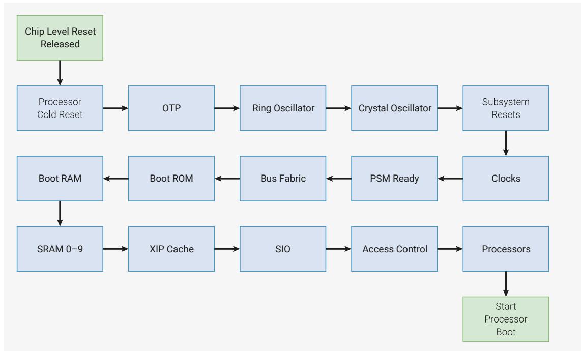
Figure 27. Power-on State Machine Sequence
graph TD
    A[Chip Level Reset Released] --> B[Processor Cold Reset]
    B --> C[OTP]
    C --> D[Ring Oscillator]
    D --> E[Crystal Oscillator]
    E --> F[Subsystem Resets]
    F --> G[Clocks]
    G --> H[PSM Ready]
    H --> I[Bus Fabric]
    I --> J[Boot ROM]
    J --> K[Boot RAM]
    K --> L[SRAM 0-9]
    L --> M[XIP Cache]
    M --> N[SIO]
    N --> O[Access Control]
    O --> P[Processors]
    P --> Q[Start Processor Boot]
System Resets apply to components essential to processor operation. System components have interdependencies, therefore their resets are de-asserted in sequence by the Power-on State Machine (PSM). Each stage of the sequencer outputs a reset done signal when complete,
rst_done
, which releases the reset input to the next stage. A partial sequence runs after a write to the
FRCE_OFF
register or a watchdog timeout. Note that the
FRCE_ON
register is intended for internal use only and is disabled in production devices.
The Power-on State Machine sequences system-level reset release following a power-up of the switched core power domain. It is distinct from the power manager (POWMAN) which controls power domain switching, see Section 6.2, “Power management” .
7.4.1. Reset sequence
Following a chip-level reset, the Power-on State Machine (PSM):
- 1. Removes cold reset to processors.
- 2. Takes OTP out of reset. OTP reads any content required to boot and asserts
rst_done. - 3. Starts the Ring Oscillator. Asserts
rst_doneonce the oscillator output is stable. - 4. Removes Crystal Oscillator (XOSC) controller reset. The XOSC does not start yet, so
rst_doneis asserted immediately. - 5. Deasserts the master subsystem reset, but does not remove individual subsystem resets.
- 6. Starts the
clk_refandclk_sysclock generators. In the initial configuration,clk_refruns from the ring oscillator with no divider andclk_sysruns fromclk_ref. - 7. The PSM confirms the clocks are active.
- 8. Removes Bus Fabric reset and initialises logic.
- 9. Removes various memory controllers' resets and initialises logic.
- 10. Removes Single-cycle IO subsystem (SIO) reset and initialises logic.
- 11. Removes Access Controller reset and initialises logic.
- 12. Deasserts Processor Complex reset. Both core 0 and core 1 start executing the boot code from ROM. The boot code reads the core id and core 1 sleeps, leaving core 0 to continue bootrom execution.
Following a watchdog reset trigger, the PSM restarts from a point selected by the PSM WDSEL register.
7.4.2. Register control
The PSM is a fully automated piece of hardware: it requires no input from the user to work. The debugger can trigger a full or partial sequence by writing to the FRCE_OFF register. The FRCE_ON register is a development feature that does nothing in production devices.
7.4.3. Interaction with watchdog
The watchdog can trigger a full or partial sequence by writing to the WDSEL register.
7.4.4. List of registers
The PSM registers start at a base address of 0x40018000 (defined as PSM_BASE in SDK).
Table 529. List of PSM registers
| Offset | Name | Info |
|---|---|---|
| 0x0 | FRCE_ON | Force block out of reset (i.e. power it on) |
| 0x4 | FRCE_OFF | Force into reset (i.e. power it off) |
| 0x8 | WDSEL | Set to 1 if the watchdog should reset this |
| 0xc | DONE | Is the subsystem ready? |
PSM: FRCE_ON Register
Offset: 0x0
Description
Force block out of reset (i.e. power it on)
Table 530. FRCE_ON Register
| Bits | Description | Type | Reset |
|---|---|---|---|
| 31:25 | Reserved. | - | - |
| 24 | PROC1 | RW | 0x0 |
| 23 | PROC0 | RW | 0x0 |
| 22 | ACCESSCTRL | RW | 0x0 |
| 21 | SIO | RW | 0x0 |
| 20 | XIP | RW | 0x0 |
| 19 | SRAM9 | RW | 0x0 |
| 18 | SRAM8 | RW | 0x0 |
| 17 | SRAM7 | RW | 0x0 |
| 16 | SRAM6 | RW | 0x0 |
| 15 | SRAM5 | RW | 0x0 |
| 14 | SRAM4 | RW | 0x0 |
| 13 | SRAM3 | RW | 0x0 |
| 12 | SRAM2 | RW | 0x0 |
| Bits | Description | Type | Reset |
|---|---|---|---|
| 11 | SRAM1 | RW | 0x0 |
| 10 | SRAM0 | RW | 0x0 |
| 9 | BOOTRAM | RW | 0x0 |
| 8 | ROM | RW | 0x0 |
| 7 | BUSFABRIC | RW | 0x0 |
| 6 | PSM_READY | RW | 0x0 |
| 5 | CLOCKS | RW | 0x0 |
| 4 | RESETS | RW | 0x0 |
| 3 | XOSC | RW | 0x0 |
| 2 | ROSC | RW | 0x0 |
| 1 | OTP | RW | 0x0 |
| 0 | PROC_COLD | RW | 0x0 |
PSM: FRCE_OFF Register
Offset: 0x4
Description
Force into reset (i.e. power it off)
Table 531. FRCE_OFF Register
| Bits | Description | Type | Reset |
|---|---|---|---|
| 31:25 | Reserved. | - | - |
| 24 | PROC1 | RW | 0x0 |
| 23 | PROC0 | RW | 0x0 |
| 22 | ACCESSCTRL | RW | 0x0 |
| 21 | SIO | RW | 0x0 |
| 20 | XIP | RW | 0x0 |
| 19 | SRAM9 | RW | 0x0 |
| 18 | SRAM8 | RW | 0x0 |
| 17 | SRAM7 | RW | 0x0 |
| 16 | SRAM6 | RW | 0x0 |
| 15 | SRAM5 | RW | 0x0 |
| 14 | SRAM4 | RW | 0x0 |
| 13 | SRAM3 | RW | 0x0 |
| 12 | SRAM2 | RW | 0x0 |
| 11 | SRAM1 | RW | 0x0 |
| 10 | SRAM0 | RW | 0x0 |
| 9 | BOOTRAM | RW | 0x0 |
| 8 | ROM | RW | 0x0 |
| Bits | Description | Type | Reset |
|---|---|---|---|
| 7 | BUSFABRIC | RW | 0x0 |
| 6 | PSM_READY | RW | 0x0 |
| 5 | CLOCKS | RW | 0x0 |
| 4 | RESETS | RW | 0x0 |
| 3 | XOSC | RW | 0x0 |
| 2 | ROSC | RW | 0x0 |
| 1 | OTP | RW | 0x0 |
| 0 | PROC_COLD | RW | 0x0 |
PSM: WDSEL Register
Offset: 0x8
Description
Set to 1 if the watchdog should reset this
Table 532. WDSEL Register
| Bits | Description | Type | Reset |
|---|---|---|---|
| 31:25 | Reserved. | - | - |
| 24 | PROC1 | RW | 0x0 |
| 23 | PROC0 | RW | 0x0 |
| 22 | ACCESSCTRL | RW | 0x0 |
| 21 | SIO | RW | 0x0 |
| 20 | XIP | RW | 0x0 |
| 19 | SRAM9 | RW | 0x0 |
| 18 | SRAM8 | RW | 0x0 |
| 17 | SRAM7 | RW | 0x0 |
| 16 | SRAM6 | RW | 0x0 |
| 15 | SRAM5 | RW | 0x0 |
| 14 | SRAM4 | RW | 0x0 |
| 13 | SRAM3 | RW | 0x0 |
| 12 | SRAM2 | RW | 0x0 |
| 11 | SRAM1 | RW | 0x0 |
| 10 | SRAM0 | RW | 0x0 |
| 9 | BOOTRAM | RW | 0x0 |
| 8 | ROM | RW | 0x0 |
| 7 | BUSFABRIC | RW | 0x0 |
| 6 | PSM_READY | RW | 0x0 |
| 5 | CLOCKS | RW | 0x0 |
| 4 | RESETS | RW | 0x0 |
| Bits | Description | Type | Reset |
|---|---|---|---|
| 3 | XOSC | RW | 0x0 |
| 2 | ROSC | RW | 0x0 |
| 1 | OTP | RW | 0x0 |
| 0 | PROC_COLD | RW | 0x0 |
PSM: DONE Register
Offset: 0xc
Description
Is the subsystem ready?
Table 533. DONE Register
| Bits | Description | Type | Reset |
|---|---|---|---|
| 31:25 | Reserved. | - | - |
| 24 | PROC1 | RO | 0x0 |
| 23 | PROC0 | RO | 0x0 |
| 22 | ACCESSCTRL | RO | 0x0 |
| 21 | SIO | RO | 0x0 |
| 20 | XIP | RO | 0x0 |
| 19 | SRAM9 | RO | 0x0 |
| 18 | SRAM8 | RO | 0x0 |
| 17 | SRAM7 | RO | 0x0 |
| 16 | SRAM6 | RO | 0x0 |
| 15 | SRAM5 | RO | 0x0 |
| 14 | SRAM4 | RO | 0x0 |
| 13 | SRAM3 | RO | 0x0 |
| 12 | SRAM2 | RO | 0x0 |
| 11 | SRAM1 | RO | 0x0 |
| 10 | SRAM0 | RO | 0x0 |
| 9 | BOOTRAM | RO | 0x0 |
| 8 | ROM | RO | 0x0 |
| 7 | BUSFABRIC | RO | 0x0 |
| 6 | PSM_READY | RO | 0x0 |
| 5 | CLOCKS | RO | 0x0 |
| 4 | RESETS | RO | 0x0 |
| 3 | XOSC | RO | 0x0 |
| 2 | ROSC | RO | 0x0 |
| 1 | OTP | RO | 0x0 |
| 0 | PROC_COLD | RO | 0x0 |
7.5. Subsystem resets
7.5.1. Overview
The reset controller allows software to reset non-critical components in RP2350. The reset controller can reset the following components:
- • USB Controller
- • PIO
- • Peripherals, including UART, I2C, SPI, PWM, Timer, ADC
- • PLLs
- • IO and Pad registers
For a full list of components that can be reset using the reset controller, see the register descriptions ( Section 7.5.3, “List of Registers” ).
When reset, components are held in reset at power-up. To use the component, software must deassert the reset.
 NOTE
NOTE
The SDK automatically deasserts some components after a reset.
7.5.2. Programmer’s model
The SDK uses the following struct to represent the resets registers:
SDK: https://github.com/raspberrypi/pico-sdk/blob/master/src/rp2350/hardware_structs/include/hardware/structs/resets.h Lines 63 - 159
63 typedef struct {
64     _REG_(RESETS_RESET_OFFSET) // RESETS_RESET
65     // 0x10000000 [28] USBCTRL      (1)
66     // 0x08000000 [27] UART1        (1)
67     // 0x04000000 [26] UART0        (1)
68     // 0x02000000 [25] TRNG         (1)
69     // 0x01000000 [24] TIMER1        (1)
70     // 0x00800000 [23] TIMER0        (1)
71     // 0x00400000 [22] TBMAN         (1)
72     // 0x00200000 [21] SYSINFO       (1)
73     // 0x00100000 [20] SYSCFG        (1)
74     // 0x00080000 [19] SPI1          (1)
75     // 0x00040000 [18] SPI0          (1)
76     // 0x00020000 [17] SHA256        (1)
77     // 0x00010000 [16] PWM           (1)
78     // 0x00008000 [15] PLL_USB       (1)
79     // 0x00004000 [14] PLL_SYS       (1)
80     // 0x00002000 [13] PIO2          (1)
81     // 0x00001000 [12] PIO1          (1)
82     // 0x00000800 [11] PIO0          (1)
83     // 0x00000400 [10] PADS_QSPI     (1)
84     // 0x00000200 [9]  PADS_BANK0    (1)
85     // 0x00000100 [8]  JTAG          (1)
86     // 0x00000080 [7]  IO_QSPI       (1)
87     // 0x00000040 [6]  IO_BANK0      (1)
88     // 0x00000020 [5]  I2C1          (1)
89     // 0x00000010 [4]  I2C0          (1)
90     // 0x00000008 [3]  HSTX          (1)
91 // 0x00000004 [2] DMA (1)
92 // 0x00000002 [1] BUSCTRL (1)
93 // 0x00000001 [0] ADC (1)
94 io_rw_32 reset;
95
96 _REG_(RESETS_WDSEL_OFFSET) // RESETS_WDSEL
97 // 0x10000000 [28] USBCTRL (0)
98 // 0x08000000 [27] UART1 (0)
99 // 0x04000000 [26] UART0 (0)
100 // 0x02000000 [25] TRNG (0)
101 // 0x01000000 [24] TIMER1 (0)
102 // 0x00800000 [23] TIMER0 (0)
103 // 0x00400000 [22] TBMAN (0)
104 // 0x00200000 [21] SYSINFO (0)
105 // 0x00100000 [20] SYSCFG (0)
106 // 0x00080000 [19] SPI1 (0)
107 // 0x00040000 [18] SPI0 (0)
108 // 0x00020000 [17] SHA256 (0)
109 // 0x00010000 [16] PWM (0)
110 // 0x00008000 [15] PLL_USB (0)
111 // 0x00004000 [14] PLL_SYS (0)
112 // 0x00002000 [13] PIO2 (0)
113 // 0x00001000 [12] PIO1 (0)
114 // 0x00000800 [11] PIO0 (0)
115 // 0x00000400 [10] PADS_QSPI (0)
116 // 0x00000200 [9] PADS_BANK0 (0)
117 // 0x00000100 [8] JTAG (0)
118 // 0x00000080 [7] IO_QSPI (0)
119 // 0x00000040 [6] IO_BANK0 (0)
120 // 0x00000020 [5] I2C1 (0)
121 // 0x00000010 [4] I2C0 (0)
122 // 0x00000008 [3] HSTX (0)
123 // 0x00000004 [2] DMA (0)
124 // 0x00000002 [1] BUSCTRL (0)
125 // 0x00000001 [0] ADC (0)
126 io_rw_32 wdsel;
127
128 _REG_(RESETS_RESET_DONE_OFFSET) // RESETS_RESET_DONE
129 // 0x10000000 [28] USBCTRL (0)
130 // 0x08000000 [27] UART1 (0)
131 // 0x04000000 [26] UART0 (0)
132 // 0x02000000 [25] TRNG (0)
133 // 0x01000000 [24] TIMER1 (0)
134 // 0x00800000 [23] TIMER0 (0)
135 // 0x00400000 [22] TBMAN (0)
136 // 0x00200000 [21] SYSINFO (0)
137 // 0x00100000 [20] SYSCFG (0)
138 // 0x00080000 [19] SPI1 (0)
139 // 0x00040000 [18] SPI0 (0)
140 // 0x00020000 [17] SHA256 (0)
141 // 0x00010000 [16] PWM (0)
142 // 0x00008000 [15] PLL_USB (0)
143 // 0x00004000 [14] PLL_SYS (0)
144 // 0x00002000 [13] PIO2 (0)
145 // 0x00001000 [12] PIO1 (0)
146 // 0x00000800 [11] PIO0 (0)
147 // 0x00000400 [10] PADS_QSPI (0)
148 // 0x00000200 [9] PADS_BANK0 (0)
149 // 0x00000100 [8] JTAG (0)
150 // 0x00000080 [7] IO_QSPI (0)
151 // 0x00000040 [6] IO_BANK0 (0)
152 // 0x00000020 [5] I2C1 (0)
153 // 0x00000010 [4] I2C0 (0)
154 // 0x00000008 [3] HSTX (0)
155 // 0x00000004 [2] DMA (0)
156 // 0x00000002 [1] BUSCTRL (0)
157 // 0x00000001 [0] ADC (0)
158 io_ro_32 reset_done;
159 } resets_hw_t;
This struct defines the following registers:
- • reset : This register contains a bit for each component that can be reset. When set to 1 , the reset is asserted. If the bit is cleared, the reset is deasserted.
- • wdset : This register contains a bit for each component that can be reset. When set to 1 , this component will reset if the watchdog fires. If you reset the power-on state machine, the entire reset controller will reset, which includes every component.
- • reset_done : This register contains a bit for each component that is automatically set when the component is out of reset. This allows software to wait for this status bit in case the component requires initialisation before use.
The SDK defines reset functions as follows:
SDK: https://github.com/raspberrypi/pico-sdk/blob/master/src/rp2_common/hardware_resets/include/hardware/resets.h Lines 159 - 161
159 static __force_inline void reset_block(uint32_t bits) {
160     reset_block_mask(bits);
161 }
SDK: https://github.com/raspberrypi/pico-sdk/blob/master/src/rp2_common/hardware_resets/include/hardware/resets.h Lines 163 - 165
163 static __force_inline void unreset_block(uint32_t bits) {
164     unreset_block_mask(bits);
165 }
SDK: https://github.com/raspberrypi/pico-sdk/blob/master/src/rp2_common/hardware_resets/include/hardware/resets.h Lines 167 - 169
167 static __force_inline void unreset_block_wait(uint32_t bits) {
168     return unreset_block_mask_wait_blocking(bits);
169 }
One example use of reset functions is the UART driver, which defines a uart_reset function that selects a different bit of the reset register depending on the UART specified:
SDK: https://github.com/raspberrypi/pico-sdk/blob/master/src/rp2_common/hardware_uart/uart.c Lines 32 - 38
32 static inline void uart_reset(uart_inst_t *uart) {
33     reset_block_num(uart_get_reset_num(uart));
34 }
35
36 static inline void uart_unreset(uart_inst_t *uart) {
37     unreset_block_num_wait_blocking(uart_get_reset_num(uart));
38 }
7.5.3. List of Registers
The reset controller registers start at a base address of 0x40020000 (defined as RESETS_BASE in SDK).
Table 534. List of RESETS registers
| Bits Register 31:28 27 26 25 24 | Description QSPI_SD QSPI_CSN QSPI_SCK USB_DM USB_DP | Type WO WO WO WO WO | Reset 0x0 0x0 0x0 0x0 0x0 |
|---|---|---|---|
| 31:29 | Reserved. | - | - |
| 28 | USBCTRL | RW | 0x1 |
| 27 | UART1 | RW | 0x1 |
| 26 | UART0 | RW | 0x1 |
| 25 | TRNG | RW | 0x1 |
| 24 | TIMER1 | RW | 0x1 |
| 23 | TIMER0 | RW | 0x1 |
| 22 | TBMAN | RW | 0x1 |
| 21 | SYSINFO | RW | 0x1 |
| 20 | SYSCFG | RW | 0x1 |
| 19 | SPI1 | RW | 0x1 |
| 18 | SPI0 | RW | 0x1 |
| 17 | SHA256 | RW | 0x1 |
| 16 | PWM | RW | 0x1 |
| 15 | PLL_USB | RW | 0x1 |
| 14 | PLL_SYS | RW | 0x1 |
| 13 | PIO2 | RW | 0x1 |
| 12 | PIO1 | RW | 0x1 |
| 11 | PIO0 | RW | 0x1 |
| 10 | PADS_QSPI | RW | 0x1 |
| 9 | PADS_BANK0 | RW | 0x1 |
| 8 | JTAG | RW | 0x1 |
| 7 | IO_QSPI | RW | 0x1 |
| 6 | IO_BANK0 | RW | 0x1 |
| 5 | I2C1 | RW | 0x1 |
| 4 | I2C0 | RW | 0x1 |
| 3 | HSTX | RW | 0x1 |
| 2 | DMA | RW | 0x1 |
| 1 | BUSCTRL | RW | 0x1 |
RESETS: RESET Register
Offset: 0x0
Table 535. RESET Register
| Bits Register 31:28 27 26 25 24 | Description QSPI_SD QSPI_CSN QSPI_SCK USB_DM USB_DP | Type WO WO WO WO WO | Reset 0x0 0x0 0x0 0x0 0x0 |
|---|---|---|---|
| 31:29 | Reserved. | - | - |
| 28 | USBCTRL | RW | 0x0 |
| 27 | UART1 | RW | 0x0 |
| 26 | UART0 | RW | 0x0 |
| 25 | TRNG | RW | 0x0 |
| 24 | TIMER1 | RW | 0x0 |
| 23 | TIMER0 | RW | 0x0 |
| 22 | TBMAN | RW | 0x0 |
| 21 | SYSINFO | RW | 0x0 |
| 20 | SYSCFG | RW | 0x0 |
| 19 | SPI1 | RW | 0x0 |
| 18 | SPI0 | RW | 0x0 |
| 17 | SHA256 | RW | 0x0 |
| 16 | PWM | RW | 0x0 |
| 15 | PLL_USB | RW | 0x0 |
| 14 | PLL_SYS | RW | 0x0 |
| 13 | PIO2 | RW | 0x0 |
| 12 | PIO1 | RW | 0x0 |
| 11 | PIO0 | RW | 0x0 |
| 10 | PADS_QSPI | RW | 0x0 |
| 9 | PADS_BANK0 | RW | 0x0 |
| 8 | JTAG | RW | 0x0 |
| 7 | IO_QSPI | RW | 0x0 |
| 6 | IO_BANK0 | RW | 0x0 |
| 5 | I2C1 | RW | 0x0 |
| 4 | I2C0 | RW | 0x0 |
| 3 | HSTX | RW | 0x0 |
| 2 | DMA | RW | 0x0 |
| 1 | BUSCTRL | RW | 0x0 |
| 0 | ADC | RW | 0x0 |
RESETS: WDSEL Register
Offset: 0x4
Table 536. WDSEL Register
RESETS: RESET_DONE Register
Offset: 0x8
Table 537.RESET_DONE Register
| Bits Register 31:28 27 26 25 24 | Description QSPI_SD QSPI_CSN QSPI_SCK USB_DM USB_DP | Type WO WO WO WO WO | Reset 0x0 0x0 0x0 0x0 0x0 |
|---|---|---|---|
| 31:29 | Reserved. | - | - |
| 28 | USBCTRL | RO | 0x0 |
| 27 | UART1 | RO | 0x0 |
| 26 | UART0 | RO | 0x0 |
| 25 | TRNG | RO | 0x0 |
| 24 | TIMER1 | RO | 0x0 |
| 23 | TIMER0 | RO | 0x0 |
| 22 | TBMAN | RO | 0x0 |
| 21 | SYSINFO | RO | 0x0 |
| 20 | SYSCFG | RO | 0x0 |
| 19 | SPI1 | RO | 0x0 |
| 18 | SPI0 | RO | 0x0 |
| 17 | SHA256 | RO | 0x0 |
| 16 | PWM | RO | 0x0 |
| 15 | PLL_USB | RO | 0x0 |
| 14 | PLL_SYS | RO | 0x0 |
| 13 | PIO2 | RO | 0x0 |
| 12 | PIO1 | RO | 0x0 |
| 11 | PIO0 | RO | 0x0 |
| 10 | PADS_QSPI | RO | 0x0 |
| 9 | PADS_BANK0 | RO | 0x0 |
| 8 | JTAG | RO | 0x0 |
| 7 | IO_QSPI | RO | 0x0 |
| 6 | IO_BANK0 | RO | 0x0 |
| 5 | I2C1 | RO | 0x0 |
| 4 | I2C0 | RO | 0x0 |
| 3 | HSTX | RO | 0x0 |
| 2 | DMA | RO | 0x0 |
| 1 | BUSCTRL | RO | 0x0 |
| 0 | ADC | RO | 0x0 |
7.6. Power-on resets and brownout detection
7.6.1. Power-on reset (POR)
The power-on reset block ensures the chip starts up cleanly when power is first applied. It accomplishes this by holding the chip in reset until the digital core supply ( DVDD ) reaches a voltage high enough to reliably power the chip’s core logic. The block holds its por_n output low until DVDD exceeds the power-on reset threshold ( \( DVDD_{TH,POR} \) ) for a period greater than the power-on reset assertion delay ( \( t_{POR,ASSERT} \) ). Once high, por_n remains high even if DVDD subsequently falls below \( DVDD_{TH,POR} \) . The behaviour of por_n when power is applied is shown in Figure 28, “A power-on reset cycle” .
Figure 28. A power-on reset cycle
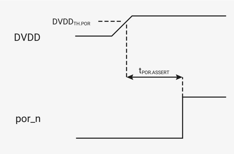
The diagram shows two signals over time. The top signal is DVDD , which starts at a low level, rises to a threshold level indicated by a dashed line labeled \( DVDD_{TH,POR} \) , and then continues to rise. The bottom signal is por_n , which is initially low. When DVDD reaches the threshold, por_n transitions to high. A horizontal double-headed arrow labeled \( t_{POR,ASSERT} \) indicates the time interval from when DVDD reaches the threshold to when por_n transitions high. After por_n goes high, it remains high even when DVDD subsequently falls below the threshold.
\( DVDD_{TH,POR} \) is fixed at a nominal 0.957V, which should result in a threshold between 0.924V and 0.99V. The threshold assumes a nominal DVDD of 1.1V at initial power-on, and por_n may never go high if a lower voltage is used. Once the chip is out of reset, DVDD can be reduced without por_n going low.
7.6.1.1. Detailed specifications
Table 538. Power-on Reset Parameters
| Parameter | Description | Min | Typ | Max | Units |
|---|---|---|---|---|---|
| \( DVDD_{TH,POR} \) | power-on reset threshold | 0.924 | 0.957 | 0.99 | V |
| \( t_{POR,ASSERT} \) | power-on reset assertion delay | 3 | 10 | µs |
7.6.2. Brownout detection (BOD)
The brownout detection block prevents unreliable operation when the digital core supply ( DVDD ) drops below a safe operating level. If enabled, the block resets the chip by taking its bor_n output low when DVDD drops below the brownout detection assertion threshold ( \( DVDD_{TH,BOD,ASSERT} \) ) for a period greater than the brownout detection assertion delay ( \( t_{BOD,ASSERT} \) ). If DVDD subsequently rises above the brownout detection de-assertion threshold ( \( DVDD_{TH,BOD,DEASSERT} \) ) for a period greater than the brownout detection de-assertion delay ( \( t_{BOD,DEASSERT} \) ), the block releases reset by taking bor_n high. A brownout, followed by supply recovery, is shown in Figure 29, “A brownout detection cycle” .
Figure 29. A brownout detection cycle
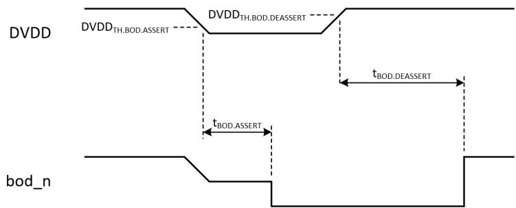
The diagram shows two signals: DVDD and bod_n. DVDD starts at a high level, drops to a low level, and then returns to high. The low level is between two thresholds: \( DVDD_{TH,BOD,ASSERT} \) and \( DVDD_{TH,BOD,DEASSERT} \) . The time DVDD is below \( DVDD_{TH,BOD,ASSERT} \) is labeled \( t_{BOD,ASSERT} \) . The time DVDD is below \( DVDD_{TH,BOD,DEASSERT} \) is labeled \( t_{BOD,DEASSERT} \) . The bod_n signal is high when DVDD is above \( DVDD_{TH,BOD,DEASSERT} \) and low when DVDD is below \( DVDD_{TH,BOD,DEASSERT} \) .
7.6.2.1. Detection enable
Brownout detection is always enabled at initial power-on. There is, however, a short delay, the brownout detection activation delay ( \( t_{BOD,ACTIVE} \) ), between por_n going high and detection becoming active. This is shown in Figure 30, “Activation of brownout detection at initial power-on and following a brownout event.”.
Figure 30. Activation of brownout detection at initial power-on and following a brownout event.
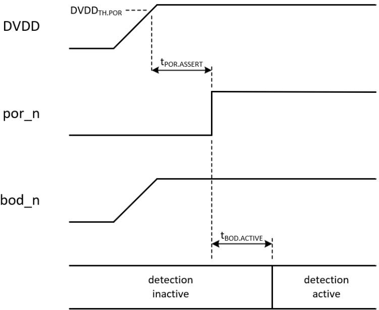
The diagram shows three signals: DVDD, por_n, and bod_n. DVDD starts at a low level, rises to a high level, and then drops to a low level before rising again. The high level is above \( DVDD_{TH,POR} \) . The time DVDD is below \( DVDD_{TH,POR} \) is labeled \( t_{POR,ASSERT} \) . The por_n signal is low when DVDD is below \( DVDD_{TH,POR} \) and high when DVDD is above \( DVDD_{TH,POR} \) . The bod_n signal is low when DVDD is below \( DVDD_{TH,POR} \) and high when DVDD is above \( DVDD_{TH,POR} \) . The time between por_n going high and bod_n becoming high is labeled \( t_{BOD,ACTIVE} \) . A table at the bottom shows the detection state: detection inactive when bod_n is low, and detection active when bod_n is high.
Once the chip is out of reset, detection can be disabled under software control. This saves a small amount of power. If detection is subsequently re-enabled, there will be another short delay, the brownout detection enable delay ( \( t_{BOD,ENABLE} \) ), before it becomes active again. This is shown in Figure 31, “Disabling and enabling brownout detection”.
Detection is disabled by writing a 0 to the EN field in the BOD register and is re-enabled by writing a 1 to the same field. The block’s bod_n output is high when detection is disabled.
Figure 31. Disabling and enabling brownout detection
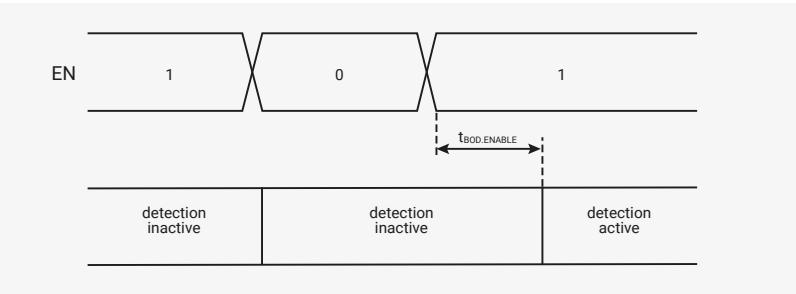
The diagram shows two signals: EN and bod_n. EN starts at 1, then drops to 0, and then returns to 1. The time EN is 0 is labeled \( t_{BOD,ENABLE} \) . The bod_n signal is high when EN is 0 and low when EN is 1. A table at the bottom shows the detection state: detection inactive when EN is 0, and detection active when EN is 1.
Detection is re-enabled if the BOD register is reset, as this sets the register’s EN field to 1. Again, detection will become
active after a delay equal to the brownout detection enable delay ( \( t_{\text{BOD,ENABLE}} \) ).
NOTE
If the BOD register is reset by a power-on or brownout-initiated reset, the delay between the register being reset and brownout detection becoming active will be equal to the brownout detection activation delay ( \( t_{\text{BOD,ACTIVE}} \) ). The delay will be equal to the brownout detection enable delay ( \( t_{\text{BOD,ENABLE}} \) ) for all other reset sources.
7.6.2.2. Adjusting the detection threshold
The brownout detection threshold ( \( \text{DVDD}_{\text{TH,BOD}} \) ) has a nominal value of 0.946V at initial power-on or after a reset event. This should result in a detection threshold between 0.913V and 0.979V. Once out of reset, the threshold can be adjusted under software control. The new detection threshold will take effect after the brownout detection programming delay ( \( t_{\text{BOD,PROG}} \) ). An example of this is shown in Figure 32, “Adjusting the brownout detection threshold” .
The threshold is adjusted by writing to the VSEL field in the BOD register. See the BOD register description for details.
NOTE
The nominal supply voltage for DVDD is 1.1 V. You should not increase the brownout detection threshold above the nominal supply voltage.
Figure 32. Adjusting the brownout detection threshold
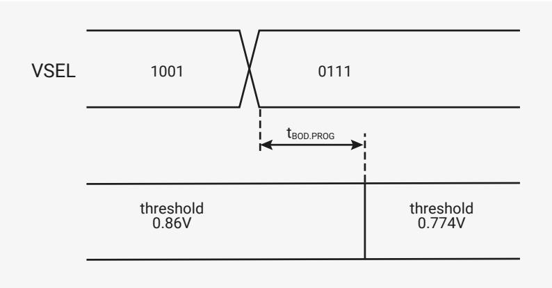
The diagram illustrates the process of adjusting the brownout detection threshold. It shows a signal labeled 'VSEL' that transitions from the value '1001' to '0111'. This transition is followed by a delay period labeled \( t_{\text{BOD,PROG}} \) . Below the VSEL signal, two horizontal lines represent the detection threshold. The first line, corresponding to the '1001' state, is labeled 'threshold 0.86V'. The second line, corresponding to the '0111' state after the programming delay, is labeled 'threshold 0.774V'.
7.6.2.3. Detailed specifications
Table 539. Brownout Detection Parameters
| Parameter | Description | Min | Typ | Max | Units |
|---|---|---|---|---|---|
| \( \text{DVDD}_{\text{TH,BOD,ASSERT}} \) | brownout detection assertion threshold | 96.5 | 100 | 103.5 | % of selected threshold voltage |
| \( \text{DVDD}_{\text{TH,BOD,DEASSERT}} \) | brownout detection de-assertion threshold | 97.4 | 101 | 105 | % of selected threshold voltage |
| \( t_{\text{BOD,ACTIVE}} \) | brownout detection activation delay | 55 | 80 | \( \mu\text{s} \) | |
| \( t_{\text{BOD,ASSERT}} \) | brownout detection assertion delay | 3 | 10 | \( \mu\text{s} \) |
| Parameter | Description | Min | Typ | Max | Units |
|---|---|---|---|---|---|
| \( t_{\text{BOD,DEASSERT}} \) | brownout detection de-assertion delay | 55 | 80 | \( \mu\text{s} \) | |
| \( t_{\text{BOD,ENABLE}} \) | brownout detection enable delay | 35 | 55 | \( \mu\text{s} \) | |
| \( t_{\text{BOD,PROG}} \) | brownout detection programming delay | 20 | 30 | \( \mu\text{s} \) |
7.6.3. Supply monitor
The power-on and brownout reset blocks are powered by the core voltage regulator’s analogue supply ( VREG_AVDD ). The blocks are initialised when power is first applied, but may not be reliably re-initialised if power is removed and then reapplied before VREG_AVDD has dropped to a sufficiently low level. To prevent this happening, VREG_AVDD is monitored and the power-on reset block is re-initialised if it drops below the VREG_AVDD activation threshold ( VREG_AVDD TH,ACTIVE ). VREG_AVDD TH,ACTIVE is fixed at a nominal 1.1V, which should result in a threshold between 0.87V and 1.26V. This threshold does not represent a safe operating voltage. Instead, it represents the voltage that VREG_AVDD must drop below to reliably re-initialise the power-on reset block. For safe operation, VREG_AVDD must be at a nominal voltage of 3.3V. See Table 1441, “Power Supply Specifications” .
7.6.3.1. Detailed specifications
Table 540. Voltage Regulator Input Supply Monitor Parameters
| Parameter | Description | Min | Typ | Max | Units |
|---|---|---|---|---|---|
| VREG_VIN TH,ACTIVE | VREG_VIN activation threshold | 0.87 | 1.1 | 1.26 | V |
7.6.4. List of registers
The chip-level reset subsystem shares a register address space with other power management subsystems in the always-on domain. The address space is referred to as POWMAN elsewhere in this document. A complete list of POWMAN registers is provided in Section 6.4, “Power management (POWMAN) registers” , but information on registers associated with the brownout detector are repeated here.
The POWMAN registers start at a base address of 0x40100000 (defined as POWMAN_BASE in SDK).