8. Clocks
8.1. Overview
The clocks block provides independent clocks to on-chip and external components. It takes inputs from a variety of clock sources, allowing the user to trade off performance against cost, board area and power consumption. From these sources it uses multiple clock generators to provide the required clocks. This architecture allows the user flexibility to start and stop clocks independently and to vary some clock frequencies whilst maintaining others at their optimum frequencies.
Figure 33. Clocks overview
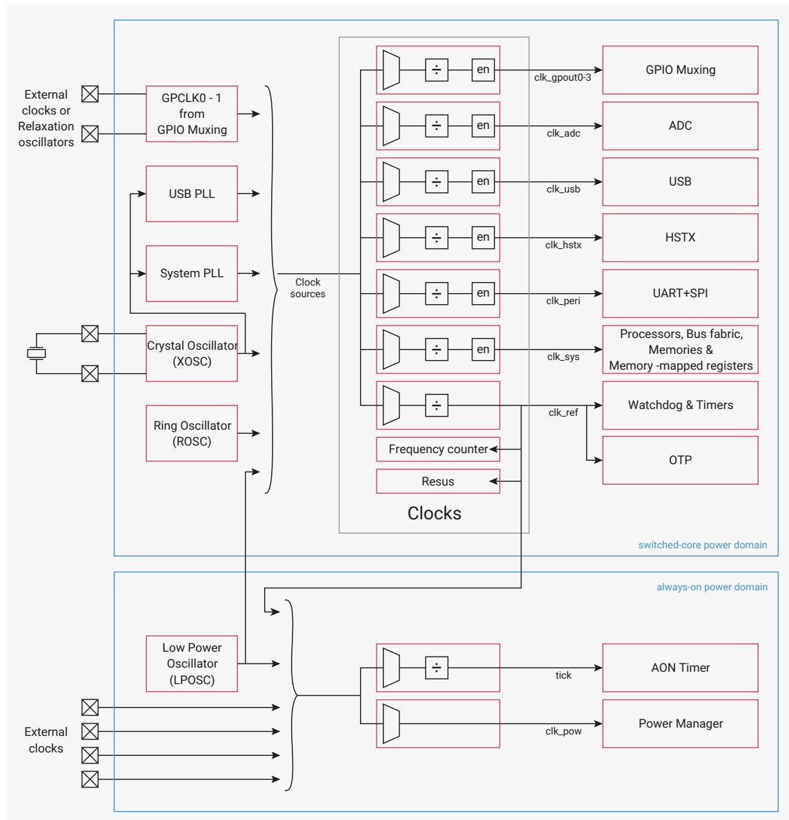
The diagram illustrates the clock system architecture, divided into two main power domains:
- switched-core power domain:
- Clock sources: External clocks or Relaxation oscillators feed into GPCLK0 - 1 from GPIO Muxing. The Crystal Oscillator (XOSC) and Ring Oscillator (ROSC) also provide inputs to the clock sources.
- PLLs: The clock sources feed into the USB PLL and System PLL.
- Clocks block:
The clock sources feed into a central 'Clocks' block, which contains:
- Seven clock dividers (represented by a trapezoid, a divider symbol, and an 'en' block) that output to:
- clk_gpout0-3 → GPIO Muxing
- clk_adc → ADC
- clk_usb → USB
- clk_hstx → HSTX
- clk_peri → UART+SPI
- clk_sys → Processors, Bus fabric, Memories & Memory-mapped registers
- clk_ref → Watchdog & Timers
- Frequency counter
- Resus
- Seven clock dividers (represented by a trapezoid, a divider symbol, and an 'en' block) that output to:
- always-on power domain:
- Low Power Oscillator (LPOSC): Receives external clocks and provides a reference to the clock sources.
- Clocks block:
The LPOSC feeds into a central 'Clocks' block, which contains:
- Two clock dividers (represented by a trapezoid and a divider symbol) that output to:
- tick → AON Timer
- clk_pow → Power Manager
- Two clock dividers (represented by a trapezoid and a divider symbol) that output to:
The crystal oscillator (XOSC) provides a reference to two PLLs, which provide high precision clocks to the processors and peripherals. These are slow to start when waking from the various low-power modes, so the on-chip ring oscillator (ROSC) is provided to boot the device until they are available. When the switched-core is powered down or the device is in DORMANT mode (see Section 6.5.3, "DORMANT state" ) the on-chip 32kHz low-power oscillator (LPOSC) provides a clock to the power manager and a tick to the Always-on Timer (AON Timer).
The clock generators select from the clock sources and optionally divide the selected clock before outputting through enable logic that provides automatic clock gating in sleep mode (see Section 8.1.3.5.2, “System sleep mode” ).
An on-chip frequency counter facilitates debugging of the clock setup and also allows measurement of the frequencies of LPOSC, ROSC and external clocks. If the system clock stops accidentally, the on-chip resus (short for resuscitate ) component restarts it from a known good clock. This allows the software debugger to access registers and debug the problem.
When the switched-core is powered, the power manager clock automatically switches to the reference clock ( clk_ref ). The user can optionally switch the AON Timer tick, though we recommend waiting until clk_ref is running from the XOSC, because the ROSC frequency is imprecise.
You can substitute the clock sources with up to 2 GPIO clock inputs. This helps avoid adding a second crystal into systems that already have an accurate clock source and enables replacement of the ROSC and LPOSC with more accurate external sources.
You can also output up to 4 generated clocks to GPIOs at up to 50MHz. This enables you to supply clocks to external devices, reducing the need for additional clock components that consume power and board area.
8.1.1. Changes between RP2350 revisions
RP2350 A3 changes the reset values of:
- • CLK_SYS_CTRL.SRC from 0 to 1 (select AUX source).
- • CLK_SYS_CTRL.AUXSRC from 0 to 2 (select ROSC as AUX source).
See Hardware changes for information about related changes made to the ROSC configuration at reset. See Bootrom changes for related changes made in the A3 boot ROM.
8.1.2. Clock sources
RP2350 can use a variety of clock sources. This flexibility allows the user to optimise the clock setup for performance, cost, board area and power consumption. RP2350 supports the following potential clock sources:
- • On-chip 32kHz low-power oscillator ( Section 8.4, “Low Power oscillator (LPOSC)” )
- • On-chip ring oscillator ( Section 8.3, “Ring oscillator (ROSC)” )
- • Crystal oscillator ( Section 8.2, “Crystal oscillator (XOSC)” )
- • External clocks from GPIOs ( Section 8.1.6.4, “Configuring a GPIO input clock” ) and PLLs ( Section 8.6, “PLL” )
The list of clock sources is different per clock generator and can be found as enumerated values in the CTRL register. See CLK_SYS_CTRL as an example.
8.1.2.1. Low-power oscillator
The on-chip 32kHz low-power oscillator ( Section 8.4, “Low Power oscillator (LPOSC)” ) requires no external components. It starts automatically when the always-on domain is powered, providing a clock for the power manager and a tick for the Always-on Timer (AON Timer) when the switched-core power domain is powered off.
The LPOSC can be tuned to 1% accuracy, and the divider in the AON Timer tick generator can further tune the 1ms tick. However, the LPOSC frequency varies with voltage and temperature, so fine-tuning is only useful in systems with stable voltage and temperature.
When the switched-core is powered, the LPOSC clock can drive the reference clock ( clk_ref ), which in turn can drive the system clock ( clk_sys ). This allows another low-power mode where the processors remain powered but, unlike the SLEEP and DORMANT modes, clocks are running. The LPOSC clock can also be sent to the frequency counter for calibration or output to a GPIO.
8.1.2.2. Ring oscillator
The on-chip ring oscillator ( Section 8.3, “Ring oscillator (ROSC)” ) requires no external components. It starts automatically when the switched-core domain is powered and is used to clock the chip during the initial boot stages. During boot, the ROSC runs at a nominal 11MHz, but varies with PVT (Process, Voltage, and Temperature). The ROSC frequency is guaranteed to be in the range 4.6MHz to 19.6MHz.
For low-cost applications where frequency accuracy is unimportant, the chip can continue to run from the ROSC. If your application requires greater performance, the frequency can be increased by programming the registers as described in Section 8.3, “Ring oscillator (ROSC)” . Because the frequency varies with PVT (Process, Voltage, and Temperature), the user must take care to avoid exceeding the maximum frequencies described in the clock generators section. For information about reducing this variation when running the ROSC at frequencies close to the maximum, see Section 8.1.2.2.1, “Mitigate ROSC frequency variation due to process” . Alternatively, use an external clock or the XOSC to provide a stable reference clock and use the PLLs to generate higher frequencies. However, this approach requires external components, which will cost board area and increase power consumption.
When using an external clock or the XOSC, you can stop the ROSC to save power. Before stopping the ROSC, you must switch the reference clock generator and the system clock generator to an alternate source.
The ROSC is unpowered when the switched-core domain is powered down, but starts immediately when the switched-core powers up. It is not affected by sleep mode. To save power, reduce the frequency before entering sleep mode. When entering DORMANT mode, the ROSC is automatically stopped. When exiting DORMANT mode, the ROSC restarts in the same configuration. If you drive clocks at close to their maximum frequencies with the ROSC, drop the frequency before entering SLEEP or DORMANT mode. This allows for frequency variation due to changes in environmental conditions during SLEEP or DORMANT mode.
To use ROSC clock externally, output it to a GPIO pin using one of the
clk_gpc1k0-3
generators.
The following sections describe techniques for mitigating PVT variation of the ROSC frequency. They also provide some interesting design challenges for use in teaching both the effects of PVT and writing software to control real time functions.
 TIP
TIP
Because the ROSC frequency varies with PVT (Process, Voltage, and Temperature), you can use the ROSC frequency to measure any one of the three PVT variables as long as you know the other two variables.
8.1.2.2.1. Mitigate ROSC frequency variation due to process
Process varies for the following reasons:
- • Chips leave the factory with a spread of process parameters. This causes variation in the ROSC frequency across chips.
- • Process parameters vary slightly as the chip ages. This is only observable over many thousands of hours of operation.
To mitigate process variation, the user can characterise individual chips and program the ROSC frequency accordingly. This is an adequate solution for small numbers of chips, but does not scale well to volume production. For high-volume applications, consider using automatic mitigation .
8.1.2.2.2. Mitigate ROSC frequency variation due to voltage
Supply voltage varies for the following reasons:
- • The power supply itself can vary.
- • As chip activity varies, on-chip IR varies.
To mitigate voltage variation, calibrate for the minimum performance target of your application, then adjust the ROSC
frequency to always exceed that minimum.
8.1.2.2.3. Mitigate ROSC frequency variation due to temperature
Temperature varies for the following reasons:
- • The ambient temperature can vary.
- • The chip temperature varies as chip activity varies due to self-heating.
To mitigate temperature variations, stabilise the temperature. You can use a temperature controlled environment, passive cooling, or active cooling. Alternatively, track the temperature using the on-chip temperature sensor and adjust the ROSC frequency so it remains within the required bounds.
8.1.2.2.4. Automatic mitigation of ROSC frequency variation due to PVT
Techniques for automatic ROSC frequency control avoid the need to calibrate individual chips, but require periodic access to a clock reference or to a time reference.
If a clock reference is available, you can use it to periodically measure the ROSC frequency and adjust accordingly. The on-chip XOSC is one potential clock reference. You can even run the XOSC intermittently to save power for very low-power application where it is too costly to run the XOSC continuously or use the PLLs to achieve high frequencies.
If a time reference is available, you can clock the on-chip AON Timer from the ROSC and periodically compare it against the time reference, adjusting the ROSC frequency as necessary. Using these techniques, the ROSC frequency still drifts due to voltage and temperature variation. As a result, you should also implement mitigations for voltage and temperature to ensure that variations do not allow the ROSC frequency to drift out of the acceptable range.
8.1.2.2.5. Automatic overclocking using the ROSC
The datasheet maximum frequencies for any digital device are quoted for worst case PVT. Most chips in most normal environments can run significantly faster than the quoted maximum, and therefore support overclocking. When RP2350 runs from the ROSC, PVT affects both the ROSC and the digital components. As the ROSC gets faster, the processors can also run faster. This means the user can overclock from the ROSC, then rely on the ROSC frequency tracking with PVT variations. The tracking of ROSC frequency and the processor capability is not perfect, and currently there is insufficient data to specify a safe ROSC setting for this mode of operation, so some experimentation is required.
This mode of operation maximises processor performance, but causes variations in the time taken to complete a task. Only use overclocking for applications where this variation is acceptable. If your application uses frequency sensitive interfaces such as USB or UART, you must use the XOSC and PLL to provide a precise clock for those components.
8.1.2.3. Crystal oscillator
The Crystal Oscillator ( Section 8.2, “Crystal oscillator (XOSC)” ) provides a precise, stable clock reference and should be used where accurate timing is required and no suitable external clocks are available. The XOSC requires an external crystal component. The external crystal determines the frequency. RP2350 supports 1MHz to 50MHz crystals and the RP2350 reference design (see Hardware design with RP2350, Minimal Design Example ) uses a 12MHz crystal. Using the XOSC and the PLLs, you can run on-chip components at their maximum frequencies. Appropriate margin is built into the design to tolerate up to 1000ppm variation in the XOSC frequency.
The XOSC is unpowered when the switched-core domain is powered down. It remains inactive when the switched-core is powered up. If required, you must enable it in software. XOSC startup takes several milliseconds, and software must wait for the
XOSC_STABLE
flag to be set before starting the PLLs and changing any clock generators. Before the XOSC completes startup, output might be non-existent or exhibit very short pulse widths; this will corrupt logic if used. When XOSC startup is complete, the reference clock (
clk_ref
) and the system clock (
clk_sys
) can run from the XOSC. If you
switch the system and reference clocks to run from the XOSC, you can stop the ROSC to save power.
The XOSC is not affected by sleep mode. It automatically stops and restarts in the same configuration when entering and exiting DORMANT mode.
To use the XOSC clock externally, output it to a GPIO pin using one of the
clk_gpc1k0-clk_gpc1k03
generators. You cannot take XOSC output directly from the XIN (XI) or XOUT (XO) pins.
8.1.2.4. External clocks
If external clocks exist in the hardware design, you can use them to clock RP2350. You can use clocks individually or in conjunction with the other (internal or external) clock sources. Use XIN and one of GPIN0-GPIN1 to input external clocks.
If you drive an external clock into XIN, you don't need an external crystal. When driving an external clock into XIN, you must configure the XOSC to pass through the XIN signal. When the switched-core powers down, this configuration will be lost, but the configuration is unaffected by SLEEP and DORMANT modes. The input is limited to 50MHz, but the on-chip PLLs can synthesise higher frequencies from the XIN input if required.
GPIN0-GPIN1 can provide system and peripherals clocks, but is limited to 50MHz. This can potentially save power and allows components on RP2350 to run synchronously with external components, which simplifies data transfer between chips. If the frequency accuracy of the external clocks is poorer than 1000ppm, the generated clocks should not run at their maximum frequencies since they could exceed their design margins. Once the external clocks begin to run, the reference clock (
clk_ref
) and the system clock (
clk_sys
) can run from the external clocks and you can stop the ROSC to save power. When the switched-core powers down, GPIN0-GPIN1 configuration will be lost, but the configuration is unaffected by SLEEP and DORMANT modes.
To provide a more accurate tick to the AON Timer, use one of the GPIN0-GPIN3 inputs to replace the clock from the LPOSC. These inputs are limited to 29MHz. GPIN0-GPIN3 configuration is unaffected by switched-core power down, sleep mode, and DORMANT mode.
8.1.2.5. Relaxation oscillators
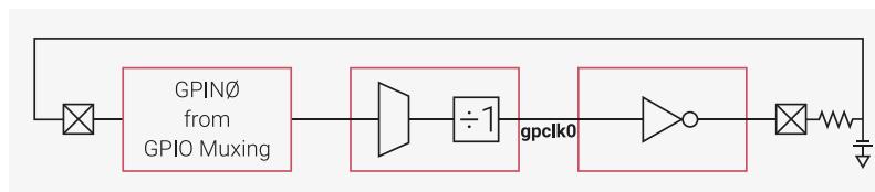
If there is no appropriate clock available, but you still want to replace or supplement external clocks with another clock source, you can construct one or two relaxation oscillators from external passive components. Send the clock source (GPIN0-GPIN1) to one of the
clk_gpc1k0-clk_gpc1k03
generators, invert it through the GPIO inverter
OUTOVER
, and connect back to the clock source input via an RC circuit:
Figure 34. Simple relaxation oscillator example
graph LR
    Input(( )) --> Mux[GPIN0 from GPIO Muxing]
    Mux --> Div[÷1]
    Div --> Inv[OUTOVER]
    Inv --> RC[RC Network]
    RC --> Input
The frequency of clocks generated from relaxation oscillators depend on the delay through the chip and the drive current from the GPIO output, both of which vary with PVT. The frequency and frequency accuracy depend on the quality and accuracy of the external components. More elaborate external components such as ceramic resonators, can improve performance, but also increase cost and complexity. Such an oscillator will not achieve 1000ppm, so they cannot drive internal clocks at their maximum frequencies. To drive internal clocks at the maximum possible frequency, use the XOSC.
The configuration of the relaxation oscillators will be lost when the switched-core powers down, but is not affected by sleep mode or DORMANT mode.
8.1.2.6. PLLs
The PLLs (Section 8.6, “PLL”) are used to provide fast clocks when running from the XOSC or an external clock source driven into the XIN pin. In a fully-featured application, the USB PLL provides a fixed 48MHz clock to the ADC and USB while
clk_ref
is driven from the XOSC or external clock source. This allows the user to drive
clk_sys
from the system PLL and vary the frequency according to demand to save power without having to change the setups of the other clocks.
clk_peri
can be driven either from the fixed frequency USB PLL or from the variable frequency system PLL. If
clk_sys
never needs to exceed 48MHz, one PLL can be used and the divider in the
clk_sys
clock generator can scale the
clk_sys
frequency according to demand.
When a PLL starts, you cannot use the output until the PLL locks as indicated by the
LOCK
bit in the
STATUS
register. As a result, the PLL output cannot be used during changes to the reference clock divider, the output dividers or the bypass mode. The output can be used during feedback divisor changes, though the output frequency might overshoot or undershoot during large changes to the feedback divisor. For more information, see Section 8.6, “PLL”.
The PLLs can drive clocks at their maximum frequency as long as the reference clock is accurate to 1000ppm, since this keeps the frequency of the generated clocks within design margins.
The PLLs are not affected by sleep mode. To save power in sleep mode, switch all clock generators away from the PLLs stop them in software before entering sleep mode.
The PLLs do not stop and restart automatically when entering and exiting DORMANT mode. If the PLLs are running when entering DORMANT mode, they will be corrupted because the reference clock in the XOSC stops. This generates out-of-control clocks that consume power unnecessarily. Before entering DORMANT mode, always switch all clock generators away from the PLLs and stop the PLLs in software.
8.1.3. Clock generators
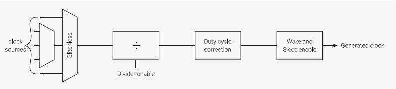
The clock generators are built on a standard design that incorporates clock source multiplexing, division, duty cycle correction, and sleep mode enabling. To save chip area and power, some individual clock generators omit certain features.
Figure 35. A generic clock generator
graph LR
    CS[clock sources] --> G[Glitchless]
    G --> D[Divider]
    DE[Divider enable] --> D
    D --> DCC[Duty cycle correction]
    DCC --> WSE[Wake and Sleep enable]
WSE --> GC[Generated clock]8.1.3.1. Instances
RP2350 has several clock generators, which are listed below.
Table 541. RP2350 clock generators
| Clock | Description | Nominal Frequency |
|---|---|---|
clk_gpout0 | Clock output to GPIO. Can be used to clock external devices or debug on chip clocks with a logic analyser or oscilloscope. | N/A |
clk_gpout1 | ||
clk_gpout2 | ||
clk_gpout3 | ||
clk_ref | Reference clock that is always running unless in DORMANT mode. Runs from ring oscillator (ROSC) at power-up but can be switched to crystal oscillator (XOSC) for more accuracy. | 6 - 12MHz |
| Clock | Description | Nominal Frequency |
|---|---|---|
clk_sys | System clock that is always running unless in DORMANT mode. Runs from
clk_ref
at power-up, but is typically switched to a PLL. | 150MHz |
clk_peri | Peripheral clock. Typically runs from
clk_sys
but allows peripherals to run at a consistent speed if
clk_sys
is changed by software. | 12 - 150MHz |
clk_usb | USB reference clock. Must be 48MHz. | 48MHz |
clk_adc | ADC reference clock. Must be 48MHz. | 48MHz |
clk_hstx | HSTX clock. | 150MHz |
For a full list of clock sources for each clock generator, see the appropriate
CTRL
register. For example,
CLK_SYS_CTRL
.
8.1.3.2. Multiplexers
All clock generators have a multiplexer referred to as the auxiliary (aux) mux. This mux has a conventional design whose output will glitch when changing the select control. The reference clock (
clk_ref
) and the system clock (
clk_sys
) have an additional multiplexer referred to as the
glitchless mux
. The glitchless mux can switch between clock sources without generating a glitch on the output.
Before switching the clock source of an auxiliary mux you must either:
- • Temporarily switch the glitchless mux away from aux (if a glitchless mux is available).
- • Temporarily disable the clock generator using its
CTRL_ENABLEbit. - • Hold the destination in reset so that a potential clock glitch doesn't cause undefined operation.
Failure to do at least one of the above can cause a glitch on the clock input of all hardware currently clocked by this clock generator. Avoid clock glitches at all costs; they can corrupt the logic running from the clock.
Clock generators require two cycles of the source clock to stop the output and two cycles of the new source to restart the output. Wait for the generator to stop before changing the auxiliary mux. When the destination clock is much slower than the system clock, there is a danger that software changes the aux mux source before the clock generator has come to a safe halt. Avoid this by polling the clock generator's
CTRL_ENABLED
status until it matches the value of
CTRL_ENABLE
.
The glitchless mux is only implemented for always-on clocks. On RP2350, the always-on clocks are the reference clock (
clk_ref
) and the system clock (
clk_sys
). Such clocks must run continuously unless the chip is in DORMANT mode. The glitchless mux has a status output (
SELECTED
) that indicates which source is selected. You can read this status output from software to confirm that a change of clock source has completed.
The recommended control sequences are as follows.
To switch between clock sources for the glitchless mux:
- 1. Switch the glitchless mux to an alternate source.
- 2. Poll the
SELECTEDregister until the switch completes.
To switch between clock sources for the aux mux when the generator has a glitchless mux:
- 1. Switch the glitchless mux to a source that isn't the aux mux.
- 2. Poll the
SELECTEDregister until the switch completes. - 3. Change the auxiliary mux select control.
- 4. Switch the glitchless mux back to the aux mux.
- 5. If required, poll the SELECTED register until the switch completes.
To switch between clock sources for the aux mux when the generator does not have a glitchless mux:
- 1. Disable the clock divider.
- 2. Wait for the generated clock to stop (two cycles of the clock source).
- 3. Change the auxiliary mux select control.
- 4. Enable the clock divider.
- 5. If required, wait for the clock generator to restart (two cycles of the clock source).
See Section 8.1.6.1, “Configuring a clock generator” for a code example of this.
8.1.3.3. Divider
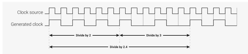
A fully featured divider divides by a fractional number in the range 1.0 to \( 2^{16} \) . Fractional division is achieved by toggling between 2 integer divisors; this yields a jittery clock that might be unsuitable for some applications. For example, when dividing by 2.4, the divider divides by 2 for 3 cycles and by 3 for 2 cycles. For divisors with large integer components, the jitter will be much smaller and less critical.
Figure 36. An example of fractional division.
All dividers support on-the-fly divisor changes : the output clock can switch cleanly from one divisor to another. The clock generator does not need to be stopped during clock divisor changes, because the dividers synchronise the divisor change to the end of the clock cycle. Similarly, dividers synchronise the enable to the end of the clock cycle to avoid glitches when the clock generator is enabled or disabled. Clock generators for always-on clocks are permanently enabled and therefore do not have an enable control.
In the event that a clock generator locks up and never completes the current clock cycle, it can be forced to stop using the KILL control. This can result in an output glitch, which can corrupt the logic driven by the clock. Always reset the destination logic before using the KILL control. Clock generators for always-on clocks are permanently active and therefore do not have a KILL control.
i NOTE
This clock generator design has been used in numerous chips and has never been known to lock up. The KILL control is inelegant and unnecessary and should not be used as an alternative to the enable.
8.1.3.4. Duty cycle correction
The divider operates on the rising edge of the input clock, so it does not generate an even duty cycle clock when dividing by odd numbers. For example, divide by 3 gives a duty cycle of 33.3%, and divide by 5 gives a duty cycle of 40%.
If enabled, duty cycle correction logic will shift the falling edge of the output clock to the falling edge of the input clock and restore a 50% duty cycle. The duty cycle correction can be enabled and disabled while the clock is running. It doesn't operate when dividing by an even number.
Figure 37. An example of duty_cycle_correction.
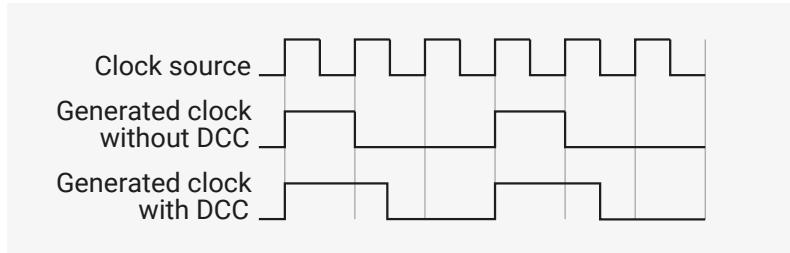
The figure is a timing diagram illustrating duty cycle correction. It contains three horizontal waveforms labeled on the left: 'Clock source', 'Generated clock without DCC', and 'Generated clock with DCC'. The 'Clock source' is a regular square wave. The 'Generated clock without DCC' has a lower duty cycle, with longer low periods. The 'Generated clock with DCC' has a higher duty cycle, with shorter low periods, demonstrating how DCC adjusts the generated clock's duty cycle to match the source.
8.1.3.5. Clock Enables
Each clock goes to multiple destinations. With a few exceptions, each destination has two enables. Use the
WAKE_EN
registers to enable the clocks when the system is awake. Use the
SLEEP_EN
registers to enable the clocks when the system is in sleep mode. Enables help reduce power in the clock distribution networks for unused components. Any component that isn't clocked will retain its configuration so it can restart quickly.
i NOTE
By default, the
WAKE_EN
and
SLEEP_EN
registers reset to
0x1
, which enables all clocks. Only use this feature for low-power designs.
8.1.3.5.1. Clock enable exceptions
The following destinations don't have clock enables:
- • The
clk_gpc1k0-clk_gpc1k03generators. - • The processor cores, because they require a clock at all times to manage their own power-saving features.
- •
clk_sys_busfabric(in wake mode), because that would prevent the cores from accessing any chip registers, including those that control the clock enables. - •
clk_sys_clocks(in wake mode), because that would prevent the cores from accessing the clocks control registers.
8.1.3.5.2. System sleep mode
System sleep mode is entered automatically when both cores are in sleep and the DMA has no outstanding transactions. In system sleep mode, the clock enables described in the previous paragraphs are switched from the
WAKE_EN
registers to the
SLEEP_EN
registers. Sleep mode helps reduce power consumed in the clock distribution networks when the chip is inactive. If the user hasn't configured the
WAKE_EN
and
SLEEP_EN
registers, system sleep does nothing.
There is little value in using system sleep without taking other measures to reduce power before the cores are put to sleep. Things to consider include:
- • Stop unused clock sources such as the PLLs and crystal oscillator.
- • Reduce the frequencies of generated clocks by increasing the clock divisors.
- • Stop external clocks.
For maximum power saving when the chip is inactive, the user should consider DORMANT (see Section 6.5.3, "DORMANT state" ) mode in which clocks are sourced from the crystal oscillator and/or the ring oscillator and those clock sources are stopped.
For more information about sleep, see Section 6.5.2, "SLEEP state" .
8.1.4. Frequency counter
The frequency counter measures the frequency of internal and external clocks by counting the clock edges seen over a test interval. The interval is defined by counting cycles of
clk_ref
, which must be driven either from XOSC or a stable external source of known frequency.
The user can pick between accuracy and test time using the
FC0_INTERVAL
register. Table 542, “Frequency Counter Test Interval vs Accuracy” shows this trade off:
Table 542. Frequency Counter Test Interval vs Accuracy
| Interval Register | Test Interval | Accuracy |
|---|---|---|
| Interval Register | shows this trade off: Test Interval | Accuracy |
| vs Accuracy 0 | 1μs | 2048kHz |
| 1 | 2μs | 1024kHz |
| 2 | 4μs | 512kHz |
| 3 | 8μs | 256kHz |
| 4 | 16μs | 128kHz |
| 5 | 32μs | 64kHz |
| 6 | 64μs | 32kHz |
| 7 | 125μs | 16kHz |
| 8 | 250μs | 8kHz |
| 9 | 500μs | 4kHz |
| 10 | 1ms | 2kHz |
| 11 | 2ms | 1kHz |
| 12 | 4ms | 500Hz |
| 13 | 8ms | 250Hz |
| 14 | 16ms | 125Hz |
| 15 | 32ms | 62.5Hz |
| It is possible to write software that inadvertently stops | clk_sys | . This normally causes an unrecoverable lock-up of the |
| lock-up, an automatic | resuscitation circuit is provided; this switches | clk_sys to a known good clock source ( clk_ref ) if it |
| detects no edges over a user-defined interval. | clk_ref can be driven from the XOSC, ROSC or an external source. The CLK_SYS_RESUS_CTRL. | |
| There is no way for resus to revive the chip if | clk_ref is also stopped. | |
| • Set the ENABLE bit in | CLK_SYS_RESUS_CTRL. | |
| • Enable the CLK_SYS_RESUS | interrupt by setting the interrupt enable bit in | INTE. |
| 8.1. Overview | 522 |
8.1.5. Resus
It is possible to write software that inadvertently stops
clk_sys
. This normally causes an unrecoverable lock-up of the cores and the on-chip debugger, leaving the user unable to trace the problem. To mitigate against unrecoverable core lock-up, an automatic
resuscitation circuit
is provided; this switches
clk_sys
to a known good clock source (
clk_ref
) if it detects no edges over a user-defined interval.
clk_ref
can be driven from the XOSC, ROSC or an external source. The interval is programmable via
CLK_SYS_RESUS_CTRL
.
 WARNING
There is no way for resus to revive the chip if
clk_ref
is also stopped.
To enable the resus:
- • Set the timeout interval.
- • Set the
ENABLEbit inCLK_SYS_RESUS_CTRL.
To detect a resus event:
- • Enable the
CLK_SYS_RESUSinterrupt by setting the interrupt enable bit inINTE.
- • Enable the
CLOCKS_DEFAULT_IRQprocessor interrupt (see Section 3.2, “Interrupts” ).
Resus is intended as a debugging aid, so the user can trace the software error that triggered the resus, then correct the error and reboot. It is possible to continue running after a resus event by reconfiguring
clk_sys
, then clearing the resus by writing the
CLEAR
bit in
CLK_SYS_RESUS_CTRL
.
⚠ WARNING
Only use resus for debugging. If
clk_sys
runs slower than expected, a resus could trigger. This could result in a
clk_sys
glitch, which could corrupt the chip.
8.1.6. Programmer’s model
8.1.6.1. Configuring a clock generator
The SDK defines an enum of clocks:
SDK: https://github.com/raspberrypi/pico-sdk/blob/master/src/rp2350/hardware_structs/include/hardware/structs/clocks.h Lines 30 - 42
30 typedef enum clock_num_rp2350 {
31     clk_gpout0 = 0, ///< Select CLK_GPOUT0 as clock source
32     clk_gpout1 = 1, ///< Select CLK_GPOUT1 as clock source
33     clk_gpout2 = 2, ///< Select CLK_GPOUT2 as clock source
34     clk_gpout3 = 3, ///< Select CLK_GPOUT3 as clock source
35     clk_ref = 4,   ///< Select CLK_REF as clock source
36     clk_sys = 5,   ///< Select CLK_SYS as clock source
37     clk_peri = 6,  ///< Select CLK_PERI as clock source
38     clk_hstx = 7,  ///< Select CLK_HSTX as clock source
39     clk_usb = 8,   ///< Select CLK_USB as clock source
40     clk_adc = 9,   ///< Select CLK_ADC as clock source
41     CLK_COUNT
42 } clock_num_t;
Additionally, the SDK defines a struct to describe the registers of a clock generator:
SDK: https://github.com/raspberrypi/pico-sdk/blob/master/src/rp2350/hardware_structs/include/hardware/structs/clocks.h Lines 116 - 137
116 typedef struct {
117     _REG_(CLOCKS_CLK_GPOUT0_CTRL_OFFSET) // CLOCKS_CLK_GPOUT0_CTRL
118     // Clock control, can be changed on-the-fly (except for auxsrc)
119     // 0x10000000 [28]  ENABLED      (0) clock generator is enabled
120     // 0x00100000 [20]  NUDGE        (0) An edge on this signal shifts the phase of the
121     //                   output by...
122     // 0x00300000 [17:16] PHASE       (0x0) This delays the enable signal by up to 3 cycles
123     //                   of the...
124     // 0x00010000 [12]   DC50        (0) Enables duty cycle correction for odd divisors, can
125     //                   be...
126     // 0x00000000 [11]   ENABLE      (0) Starts and stops the clock generator cleanly
127     // 0x00000400 [10]   KILL        (0) Asynchronously kills the clock generator, enable
128     //                   must be...
129     // 0x000001e0 [8:5]  AUXSRC      (0x0) Selects the auxiliary clock source, will glitch
130     //                   when switching
131     io_rw_32 ctrl;
132
133     _REG_(CLOCKS_CLK_GPOUT0_DIV_OFFSET) // CLOCKS_CLK_GPOUT0_DIV
134     // 0xffff0000 [31:16] INT        (0x0001) Integer part of clock divisor, 0 -> max+1, can
135     //                   be...
136     // 0x000fffff [15:0]  FRAC       (0x0000) Fractional component of the divisor, can be
    changed on-the-fly
131     io_rw_32 div;
132
133     _REG_(CLOCKS_CLK_GPOUT0_SELECTED_OFFSET) // CLOCKS_CLK_GPOUT0_SELECTED
134     // Indicates which src is currently selected (one-hot)
135     // 0x00000001 [0]     CLK_GPOUT0_SELECTED (1) This slice does not have a glitchless mux
    (only the...
136     io_ro_32 selected;
137 } clock_hw_t;
Clock configuration requires the following pieces of information:
- • The frequency of the clock source
- • The mux / aux mux position of the clock source
- • The desired output frequency
The SDK provides
clock_configure
to configure a clock:
SDK: https://github.com/raspberrypi/pico-sdk/blob/master/src/rp2_common/hardware_clocks/clocks.c Lines 40 - 133
40 static void clock_configure_internal(clock_handle_t clock, uint32_t src, uint32_t auxsrc,
    uint32_t actual_freq, uint32_t div) {
41     clock_hw_t *clock_hw = &clocks_hw->clk[clock];
42
43     // If increasing divisor, set divisor before source. Otherwise set source
44     // before divisor. This avoids a momentary overspeed when e.g. switching
45     // to a faster source and increasing divisor to compensate.
46     if (div > clock_hw->div)
47         clock_hw->div = div;
48
49     // If switching a glitchless slice (ref or sys) to an aux source, switch
50     // away from aux *first* to avoid passing glitches when changing aux mux.
51     // Assume (!!!) glitchless source 0 is no faster than the aux source.
52     if (has_glitchless_mux(clock) && src ==
        CLOCKS_CLK_SYS_CTRL_SRC_VALUE_CLKSRC_CLK_SYS_AUX) {
53         hw_clear_bits(&clock_hw->ctrl, CLOCKS_CLK_REF_CTRL_SRC_BITS);
54         while (!(clock_hw->selected & 1u))
55             tight_loop_contents();
56     }
57     // If no glitchless mux, cleanly stop the clock to avoid glitches
58     // propagating when changing aux mux. Note it would be a really bad idea
59     // to do this on one of the glitchless clocks (clk_sys, clk_ref).
60     else {
61         // Disable clock. On clk_ref and clk_sys this does nothing,
62         // all other clocks have the ENABLE bit in the same position.
63         hw_clear_bits(&clock_hw->ctrl, CLOCKS_CLK_GPOUT0_CTRL_ENABLE_BITS);
64         if (configured_freq[clock] > 0) {
65             // Delay for 3 cycles of the target clock, for ENABLE propagation.
66             // Note XOSC_COUNT is not helpful here because XOSC is not
67             // necessarily running, nor is timer...
68             uint delay_cyc = configured_freq[clk_sys] / configured_freq[clock] + 1;
69             busy_wait_at_least_cycles(delay_cyc * 3);
70         }
71     }
72
73     // Set aux mux first, and then glitchless mux if this clock has one
74     hw_write_masked(&clock_hw->ctrl,
75         (auxsrc << CLOCKS_CLK_SYS_CTRL_AUXSRC_LSB),
76         CLOCKS_CLK_SYS_CTRL_AUXSRC_BITS
77     );
78
79     if (has_glitchless_mux(clock)) {
80         hw_write_masked(&clock_hw->ctrl,
81             src << CLOCKS_CLK_REF_CTRL_SRC_LSB,
82             CLOCKS_CLK_REF_CTRL_SRC_BITS
83         );
84         while (!(clock_hw->selected & (1u << src)))
85             tight_loop_contents();
86     }
87
88     // Enable clock. On clk_ref and clk_sys this does nothing,
89     // all other clocks have the ENABLE bit in the same position.
90     hw_set_bits(&clock_hw->ctrl, CLOCKS_CLK_GPOUT0_CTRL_ENABLE_BITS);
91
92     // Now that the source is configured, we can trust that the user-supplied
93     // divisor is a safe value.
94     clock_hw->div = div;
95     configured_freq[clock] = actual_freq;
96 }
97
98 bool clock_configure(clock_handle_t clock, uint32_t src, uint32_t auxsrc, uint32_t src_freq,
99     uint32_t freq) {
100     assert(src_freq >= freq);
101
102     if (freq > src_freq)
103         return false;
104
105     uint64_t div64 = (((uint64_t) src_freq) << CLOCKS_CLK_GPOUT0_DIV_INT_LSB) / freq;
106     uint32_t div, actual_freq;
107     if (div64 >> 32) {
108         // set div to 0 for maximum clock divider
109         div = 0;
110         actual_freq = src_freq >> (32 - CLOCKS_CLK_GPOUT0_DIV_INT_LSB);
111     } else {
112         div = (uint32_t) div64;
113         actual_freq = (uint32_t) (((uint64_t) src_freq) << CLOCKS_CLK_GPOUT0_DIV_INT_LSB) /
114             div;
115     }
116     clock_configure_internal(clock, src, auxsrc, actual_freq, div);
117     // Store the configured frequency
118     return true;
119 }
120
121 void clock_configure_int_divider(clock_handle_t clock, uint32_t src, uint32_t auxsrc,
122     uint32_t src_freq, uint32_t int_divider) {
123     clock_configure_internal(clock, src, auxsrc, src_freq / int_divider, int_divider <<
124         CLOCKS_CLK_GPOUT0_DIV_INT_LSB);
125 }
126
127 void clock_configure_undivided(clock_handle_t clock, uint32_t src, uint32_t auxsrc, uint32_t
128     src_freq) {
129     clock_configure_internal(clock, src, auxsrc, src_freq, 1u <<
130         CLOCKS_CLK_GPOUT0_DIV_INT_LSB);
131 }
clocks_init
calls
clock_configure
for each clock. The following example shows the
clk_sys
configuration:
SDK: https://github.com/raspberrypi/pico-sdk/blob/master/src/rp2-common/pico_runtime_init/runtime_init_clocks.c Lines 100 - 104
100     // CLK SYS = PLL SYS (usually) 125MHz / 1 = 125MHz
101     clock_configure_undivided(clk_sys,
102         CLOCKS_CLK_SYS_CTRL_SRC_VALUE_CLKSRC_CLK_SYS_AUX,
103         CLOCKS_CLK_SYS_CTRL_AUXSRC_VALUE_CLKSRC_PLL_SYS,
104         SYS_CLK_HZ);
Once a clock is configured, call
clock_get_hz
to get the output frequency in Hz.
SDK: https://github.com/raspberrypi/pico-sdk/blob/master/src/rp2_common/hardware_clocks/clocks.c Lines 137 - 139
137 uint32_t clock_get_hz(clock_handle_t clock) {
138     return configured_freq[clock];
139 }
⚠ WARNING
The frequency returned by
clock_get_hz
will be inaccurate if the provided source frequency is incorrect.
8.1.6.2. Using the frequency counter
To use the frequency counter, the programmer must:
- 1. Set the reference frequency:
clk_ref. - 2. Set the mux position of the source they want to measure. See
FC0_SRC. - 3. Wait for the
DONEstatus bit inFC0_STATUSto be set. - 4. Read the result.
The SDK defines a
frequency_count
function that takes the source as an argument and returns the frequency in kHz:
SDK: https://github.com/raspberrypi/pico-sdk/blob/master/src/rp2_common/hardware_clocks/clocks.c Lines 147 - 174
147 uint32_t frequency_count_khz(uint src) {
148     fc_hw_t *fc = &clocks_hw->fc0;
149
150     // If frequency counter is running need to wait for it. It runs even if the source is NULL
151     while(fc->status & CLOCKS_FC0_STATUS_RUNNING_BITS) {
152         tight_loop_contents();
153     }
154
155     // Set reference freq
156     fc->ref_khz = clock_get_hz(clk_ref) / 1000;
157
158     // FIXME: Don't pick random interval. Use best interval
159     fc->interval = 10;
160
161     // No min or max
162     fc->min_khz = 0;
163     fc->max_khz = 0xffffffff;
164
165     // Set SRC which automatically starts the measurement
166     fc->src = src;
167
168     while(!(fc->status & CLOCKS_FC0_STATUS_DONE_BITS)) {
169         tight_loop_contents();
170     }
171
172     // Return the result
173     return fc->result >> CLOCKS_FC0_RESULT_KHZ_LSB;
174 }
There is also a wrapper function to change the unit to MHz:
SDK: https://github.com/raspberrypi/pico-sdk/blob/master/src/rp2_common/hardware_clocks/include/hardware/clocks.h Lines 377 - 379
377 static inline float frequency_count_mhz(uint src) {
378     return ((float) (frequency_count_khz(src))) / KHZ;
379 }
The frequency counter can also be used in a test mode. This allows the hardware to check if the frequency is between a minimum and a maximum frequency, set in
FC0_MIN_KHZ
and
FC0_MAX_KHZ
. This mode will set one of the following bits in
FC0_STATUS
when
DONE
is set:
- • SLOW : if the frequency is below the specified range
- • PASS : if the frequency is within the specified range
- • FAST : if the frequency is above the specified range
- • DIED : if the clock is stopped or stops running
Test mode will also set the FAIL bit if DIED , FAST , or SLOW are set.
8.1.6.3. Configuring a GPIO output clock
SDK: https://github.com/raspberrypi/pico-sdk/blob/master/src/rp2_common/hardware_clocks/clocks.c Lines 245 - 263
245 void clock_gpio_init_int_frac16(uint gpio, uint src, uint32_t div_int, uint16_t div_frac16)
246 {
247     // note this includes an invalid_params_if before defaulting to clk_gpout0
248     uint gpclk = gpio_to_gpout_clock_handle(gpio, clk_gpout0);
249     invalid_params_if(HARDWARE_CLOCKS, div_int >> REG_FIELD_WIDTH(
250         CLOCKS_CLK_GPOUT0_DIV_INT));
251     // Set up the gpclk generator
252     clocks_hw->clk[gpclk].ctrl = (src << CLOCKS_CLK_GPOUT0_CTRL_AUXSRC_LSB) |
253         CLOCKS_CLK_GPOUT0_CTRL_ENABLE_BITS;
254     #ifdef REG_FIELD_WIDTH(CLOCKS_CLK_GPOUT0_DIV_FRAC) == 16
255         clocks_hw->clk[gpclk].div = (div_int << CLOCKS_CLK_GPOUT0_DIV_INT_LSB) | (div_frac16 <<
256             CLOCKS_CLK_GPOUT0_DIV_FRAC_LSB);
257     #elif REG_FIELD_WIDTH(CLOCKS_CLK_GPOUT0_DIV_FRAC) == 8
258         clocks_hw->clk[gpclk].div = (div_int << CLOCKS_CLK_GPOUT0_DIV_INT_LSB) | ((div_frac16 <<
259             >>8u) << CLOCKS_CLK_GPOUT0_DIV_FRAC_LSB);
260     #else
261         #error unsupported number of fractional bits
262     #endif
263     // Set gpio pin to gpclock function
264     gpio_set_function(gpio, GPIO_FUNC_GPCK);
265 }
8.1.6.4. Configuring a GPIO input clock
SDK: https://github.com/raspberrypi/pico-sdk/blob/master/src/rp2_common/hardware_clocks/clocks.c Lines 300 - 330
300 bool clock_configure_gpin(clock_handle_t clock, uint gpio, uint32_t src_freq, uint32_t freq)
301 {
302     // Configure a clock to run from a GPIO input
303 }
302     uint gpin = 0;
303     if (gpio == 20) gpin = 0;
304     else if (gpio == 22) gpin = 1;
305     else if (gpio == 12) gpin = 0;
306     else if (gpio == 14) gpin = 1;
307     else {
308         invalid_params_if(HARDWARE_CLOCKS, true);
309     }
310
311     // Work out sources. GPIN is always an auxsrc
312     uint src = 0;
313
314     // GPIN1 == GPIN0 + 1
315     uint auxsrc = gpin0_src[clock] + gpin;
316
317     if (has_glitchless_mux(clock)) {
318         // AUX src is always 1
319         src = 1;
320     }
321
322     // Set the GPIO function
323     gpio_set_function(gpio, GPIO_FUNC_GPCK);
324
325     // Now we have the src, auxsrc, and configured the gpio input
326     // call clock configure to run the clock from a gpio
327     return clock_configure(clock, src, auxsrc, src_freq, freq);
328 }
8.1.6.5. Enabling resus
SDK: https://github.com/raspberrypi/pico-sdk/blob/master/src/rp2_common/hardware_clocks/clocks.c Lines 221 - 243
221 void clocks_enable_resus(resus_callback_t resus_callback) {
222     // Restart clk_sys if it is stopped by forcing it
223     // to the default source of clk_ref. If clk_ref stops running this will
224     // not work.
225
226     // Store user's resus callback
227     _resus_callback = resus_callback;
228
229     irq_set_exclusive_handler(CLOCKS_IRQ, clocks_irq_handler);
230
231     // Enable the resus interrupt in clocks
232     clocks_hw->inte = CLOCKS_INTE_CLK_SYS_RESUS_BITS;
233
234     // Enable the clocks irq
235     irq_set_enabled(CLOCKS_IRQ, true);
236
237     // 2 * clk_ref freq / clk_sys_min_freq;
238     // assume clk_ref is 3MHz and we want clk_sys to be no lower than 1MHz
239     uint timeout = 2 * 3 * 1;
240
241     // Enable resus with the maximum timeout
242     clocks_hw->resus.ctrl = CLOCKS_CLK_SYS_RESUS_CTRL_ENABLE_BITS | timeout;
243 }
8.1.6.6. Configuring sleep mode
Sleep mode is active when neither processor core nor the DMA are requesting clocks. For example, sleep mode is active when the DMA is not active and both core 0 and core 1 are waiting for an interrupt.
The
SLEEP_EN
registers set what clocks run in sleep mode. The
hello_sleep
example (
hello_sleep_aon.c
in the
pico-playground GitHub repository
) illustrates how to put the chip to sleep until the AON Timer fires.
NOTE
clk_sys
is always sent to
proc0
and
proc1
during sleep mode, as some logic must be clocked for the processor to wake up again.
Pico Extras: https://github.com/raspberrypi/pico-extras/blob/master/src/rp2_common/pico_sleep/sleep.c Lines 159 - 183
159 void sleep_goto_sleep_until(struct timespec *ts, aon_timer_alarm_handler_t callback)
160 {
161
162     // We should have already called the sleep_run_from_dormant_source function
163     // This is only needed for dormancy although it saves power running from xosc while
    sleeping
164     //assert(dormant_source_valid(_dormant_source));
165
166     clocks_hw->sleep_en0 = CLOCKS_SLEEP_EN0_CLK_REF_POWMAN_BITS;
167     clocks_hw->sleep_en1 = 0x0;
168
169     aon_timer_enable_alarm(ts, callback, false);
170
171     stdio_flush();
172
173     // Enable deep sleep at the proc
174     processor_deep_sleep();
175
176     // Go to sleep
177     __wfi();
178 }
8.1.7. List of registers
The clocks registers start at a base address of
0x40010000
(defined as
CLOCKS_BASE
in SDK).
Table 543. List of CLOCKS registers
| Offset | Name | Info |
|---|---|---|
| 0x00 | CLK_GPOUT0_CTRL | Clock control, can be changed on-the-fly (except for auxsrc) |
| 0x04 | CLK_GPOUT0_DIV | |
| 0x08 | CLK_GPOUT0_SELECTED | Indicates which src is currently selected (one-hot) |
| 0x0c | CLK_GPOUT1_CTRL | Clock control, can be changed on-the-fly (except for auxsrc) |
| 0x10 | CLK_GPOUT1_DIV | |
| 0x14 | CLK_GPOUT1_SELECTED | Indicates which src is currently selected (one-hot) |
| 0x18 | CLK_GPOUT2_CTRL | Clock control, can be changed on-the-fly (except for auxsrc) |
| 0x1c | CLK_GPOUT2_DIV | |
| 0x20 | CLK_GPOUT2_SELECTED | Indicates which src is currently selected (one-hot) |
| 0x24 | CLK_GPOUT3_CTRL | Clock control, can be changed on-the-fly (except for auxsrc) |
| Offset 0x42fc8 0x42fcc 0x42fd0 0x42fd4 0x42fd8 | Name DEVID DEVTYPE PIDR4 PIDR5 PIDR6 | Info Device Configuration register Device Type Identifier register CoreSight Periperal ID4 CoreSight Periperal ID5 CoreSight Periperal ID6 |
|---|---|---|
| 0x28 0x28 | CLK_GPOUT3_DIV CLK_GPOUT3_DIV | |
| 0x2c | CLK_GPOUT3_SELECTED | Indicates which src is currently selected (one-hot) |
| 0x30 | CLK_REF_CTRL | Clock control, can be changed on-the-fly (except for auxsrc) |
| 0x34 0x34 | CLK_REF_DIV CLK_REF_DIV | |
| 0x38 | CLK_REF_SELECTED | Indicates which src is currently selected (one-hot) |
| 0x3c | CLK_SYS_CTRL | Clock control, can be changed on-the-fly (except for auxsrc) |
| 0x40 0x40 | CLK_SYS_DIV CLK_SYS_DIV | |
| 0x44 | CLK_SYS_SELECTED | Indicates which src is currently selected (one-hot) |
| 0x48 | CLK_PERI_CTRL | Clock control, can be changed on-the-fly (except for auxsrc) |
| 0x4c 0x4c | CLK_PERI_DIV CLK_PERI_DIV | |
| 0x50 | CLK_PERI_SELECTED | Indicates which src is currently selected (one-hot) |
| 0x54 | CLK_HSTX_CTRL | Clock control, can be changed on-the-fly (except for auxsrc) |
| 0x58 0x58 | CLK_HSTX_DIV CLK_HSTX_DIV | |
| 0x5c | CLK_HSTX_SELECTED | Indicates which src is currently selected (one-hot) |
| 0x60 | CLK_USB_CTRL | Clock control, can be changed on-the-fly (except for auxsrc) |
| 0x64 0x64 | CLK_USB_DIV CLK_USB_DIV | |
| 0x68 | CLK_USB_SELECTED | Indicates which src is currently selected (one-hot) |
| 0x6c | CLK_ADC_CTRL | Clock control, can be changed on-the-fly (except for auxsrc) |
| 0x70 0x70 | CLK_ADC_DIV CLK_ADC_DIV | |
| 0x74 | CLK_ADC_SELECTED | Indicates which src is currently selected (one-hot) |
| 0x78 0x78 | DFTCLK_XOSC_CTRL DFTCLK_XOSC_CTRL | |
| 0x7c 0x7c | DFTCLK_ROSC_CTRL DFTCLK_ROSC_CTRL | |
| 0x80 0x80 | DFTCLK_LPOSC_CTRL DFTCLK_LPOSC_CTRL | |
| 0x84 0x84 | CLK_SYS_RESUS_CTRL CLK_SYS_RESUS_CTRL | |
| 0x88 0x88 | CLK_SYS_RESUS_STATUS CLK_SYS_RESUS_STATUS | |
| 0x8c | FC0_REF_KHZ | Reference clock frequency in kHz |
| 0x90 | FC0_MIN_KHZ | Minimum pass frequency in kHz. This is optional. Set to 0 if you are not using the pass/fail flags |
| 0x94 | FC0_MAX_KHZ | Maximum pass frequency in kHz. This is optional. Set to 0x1ffffff if you are not using the pass/fail flags |
| 0x98 | FC0_DELAY | Delays the start of frequency counting to allow the mux to settle Delay is measured in multiples of the reference clock period |
| 0x9c | FC0_INTERVAL | The test interval is 0.98us * 2**interval, but let’s call it 1us * 2**interval |
| 0xa0 | FC0_SRC | The default gives a test interval of 250us Clock sent to frequency counter, set to 0 when not required Writing to this register initiates the frequency count |
| 0xa4 | FC0_STATUS | Frequency counter status |
| Offset | Name | Info |
|---|---|---|
| 0xa8 | FC0_RESULT | Result of frequency measurement, only valid when status_done=1 |
| 0xac | WAKE_EN0 | enable clock in wake mode |
| 0xb0 | WAKE_EN1 | enable clock in wake mode |
| 0xb4 | SLEEP_EN0 | enable clock in sleep mode |
| 0xb8 | SLEEP_EN1 | enable clock in sleep mode |
| 0xbc | ENABLED0 | indicates the state of the clock enable |
| 0xc0 | ENABLED1 | indicates the state of the clock enable |
| 0xc4 | INTR | Raw Interrupts |
| 0xc8 | INTE | Interrupt Enable |
| 0xcc | INTF | Interrupt Force |
| 0xd0 | INTS | Interrupt status after masking & forcing |
CLOCKS: CLK_GPOUT0_CTRL Register
Offset: 0x00
Description
Clock control, can be changed on-the-fly (except for auxsrc)
Table 544.
CLK_GPOUT0_CTRL
Register
| Bits | Description | Type | Reset |
|---|---|---|---|
| 31:29 | Reserved. | - | - |
| 28 | ENABLED: clock generator is enabled | RO | 0x0 |
| 27:21 | Reserved. | - | - |
| 20 | NUDGE:
An edge on this signal shifts the phase of the output by 1 cycle of the input clock This can be done at any time | RW | 0x0 |
| 19:18 | Reserved. | - | - |
| 17:16 | PHASE:
This delays the enable signal by up to 3 cycles of the input clock This must be set before the clock is enabled to have any effect | RW | 0x0 |
| 15:13 | Reserved. | - | - |
| 12 | DC50: Enables duty cycle correction for odd divisors, can be changed on-the-fly | RW | 0x0 |
| 11 | ENABLE: Starts and stops the clock generator cleanly | RW | 0x0 |
| 10 | KILL: Asynchronously kills the clock generator, enable must be set low before deasserting kill | RW | 0x0 |
| 9 | Reserved. | - | - |
| 8:5 | AUXSRC: Selects the auxiliary clock source, will glitch when switching | RW | 0x0 |
| Enumerated values: | |||
| 0x0 → CLKSRC_PLL_SYS | |||
| 0x1 → CLKSRC_GPIN0 |
| Bits | Description | Type | Reset |
|---|---|---|---|
| 0x2 → CLKSRC_GPIN1 | |||
| 0x3 → CLKSRC_PLL_USB | |||
| 0x4 → CLKSRC_PLL_USB_PRIMARY_REF_OPCG | |||
| 0x5 → ROSC_CLKSRC | |||
| 0x6 → XOSC_CLKSRC | |||
| 0x7 → LPOSC_CLKSRC | |||
| 0x8 → CLK_SYS | |||
| 0x9 → CLK_USB | |||
| 0xa → CLK_ADC | |||
| 0xb → CLK_REF | |||
| 0xc → CLK_PERI | |||
| 0xd → CLK_HSTX | |||
| 0xe → OTP_CLK2FC | |||
| 4:0 | Reserved. | - | - |
CLOCKS: CLK_GPOUT0_DIV Register
Offset: 0x04
Table 545.
CLK_GPOUT0_DIV
Register
| Bits | Description | Type | Reset |
|---|---|---|---|
| 31:16 | INT: Integer part of clock divisor, 0 → max+1, can be changed on-the-fly | RW | 0x0001 |
| 15:0 | FRAC: Fractional component of the divisor, can be changed on-the-fly | RW | 0x0000 |
CLOCKS: CLK_GPOUT0_SELECTED Register
Offset: 0x08
Description
Indicates which src is currently selected (one-hot)
Table 546.
CLK_GPOUT0_SELECTED
Register
| Bits | Description | Type | Reset |
|---|---|---|---|
| 31:1 | Reserved. | - | - |
| 0 | This slice does not have a glitchless mux (only the AUX_SRC field is present, not SRC) so this register is hardwired to 0x1. | RO | 0x1 |
CLOCKS: CLK_GPOUT1_CTRL Register
Offset: 0x0c
Description
Clock control, can be changed on-the-fly (except for auxsrc)
Table 547.
CLK_GPOUT1_CTRL
Register
| Bits | Description | Type | Reset |
|---|---|---|---|
| 31:29 | Reserved. | - | - |
| 28 | ENABLED: clock generator is enabled | RO | 0x0 |
| Bits | Description | Type | Reset |
|---|---|---|---|
| 27:21 | Reserved. | - | - |
| 20 | NUDGE
: An edge on this signal shifts the phase of the output by 1 cycle of the input clock This can be done at any time | RW | 0x0 |
| 19:18 | Reserved. | - | - |
| 17:16 | PHASE
: This delays the enable signal by up to 3 cycles of the input clock This must be set before the clock is enabled to have any effect | RW | 0x0 |
| 15:13 | Reserved. | - | - |
| 12 | DC50 : Enables duty cycle correction for odd divisors, can be changed on-the-fly | RW | 0x0 |
| 11 | ENABLE : Starts and stops the clock generator cleanly | RW | 0x0 |
| 10 | KILL : Asynchronously kills the clock generator, enable must be set low before deasserting kill | RW | 0x0 |
| 9 | Reserved. | - | - |
| 8:5 | AUXSRC : Selects the auxiliary clock source, will glitch when switching | RW | 0x0 |
| Enumerated values: | |||
| 0x0 → CLKSRC_PLL_SYS | |||
| 0x1 → CLKSRC_GPIN0 | |||
| 0x2 → CLKSRC_GPIN1 | |||
| 0x3 → CLKSRC_PLL_USB | |||
| 0x4 → CLKSRC_PLL_USB_PRIMARY_REF_OPCG | |||
| 0x5 → ROSC_CLKSRC | |||
| 0x6 → XOSC_CLKSRC | |||
| 0x7 → LPOSC_CLKSRC | |||
| 0x8 → CLK_SYS | |||
| 0x9 → CLK_USB | |||
| 0xa → CLK_ADC | |||
| 0xb → CLK_REF | |||
| 0xc → CLK_PERI | |||
| 0xd → CLK_HSTX | |||
| 0xe → OTP_CLK2FC | |||
| 4:0 | Reserved. | - | - |
CLOCKS: CLK_GPOUT1_DIV Register
Offset: 0x10
Table 548.
CLK_GPOUT1_DIV
Register
| Bits | Description | Type | Reset |
|---|---|---|---|
| 31:16 | INT : Integer part of clock divisor, 0 → max+1, can be changed on-the-fly | RW | 0x0001 |
| Bits 31:0 Bits 31:0 Bits 31:28 | column_2 | Description Description Input value for GPIO0…31. Description QSPI_SD : Input value on QSPI SD0 (MOSI), SD1 (MISO), SD2 and SD3 pins | Type RO Type RO Type RO | Reset - Reset 0x00000000 Reset 0x0 |
|---|---|---|---|---|
| ED Register 31:1 | Reserved. | - | - | |
| 0 | This slice does not have a glitchless mux (only the AUX_SRC field is present, | RO | 0x1 | |
| CLOCK Offset | S : CLK_GPOUT2_CTRL Register : 0x18 | |||
| Table 550. Bits CLK_GPOUT2_CTRL | Description | Type | Reset | |
| Register 31:29 | Reserved. | - | - | |
| 28 | ENABLED | : clock generator is enabled | RO | 0x0 |
| 27:21 | Reserved. | - | - | |
| 20 | NUDGE | : An edge on this signal shifts the phase of the output by 1 cycle of the input clock This can be done at any time | RW | 0x0 |
| 19:18 | Reserved. | - | - | |
| 17:16 | PHASE | : This delays the enable signal by up to 3 cycles of the input clock This must be set before the clock is enabled to have any effect | RW | 0x0 |
| 15:13 | Reserved. | - | - | |
| 12 | DC50 fly | : Enables duty cycle correction for odd divisors, can be changed on-the- | RW | 0x0 |
| 11 | ENABLE | : Starts and stops the clock generator cleanly | RW | 0x0 |
| 10 | KILL | : Asynchronously kills the clock generator, enable must be set low before deasserting kill | RW | 0x0 |
| 9 | Reserved. | - | - | |
| 8:5 | AUXSRC | : Selects the auxiliary clock source, will glitch when switching Enumerated values: | RW | 0x0 |
CLOCKS: CLK_GPOUT1_SELECTED Register
Offset: 0x14
Description
Indicates which src is currently selected (one-hot)
Table 549.
CLK_GPOUT1_SELECTED Register
CLOCKS: CLK_GPOUT2_CTRL Register
Offset: 0x18
Description
Clock control, can be changed on-the-fly (except for auxsrc)
Table 550.
CLK_GPOUT2_CTRL Register
| Bits | Description | Type | Reset |
|---|---|---|---|
| 0x5 → ROSC_CLKSRC_PH | |||
| 0x6 → XOSC_CLKSRC | |||
| 0x7 → LPOSC_CLKSRC | |||
| 0x8 → CLK_SYS | |||
| 0x9 → CLK_USB | |||
| 0xa → CLK_ADC | |||
| 0xb → CLK_REF | |||
| 0xc → CLK_PERI | |||
| 0xd → CLK_HSTX | |||
| 0xe → OTP_CLK2FC | |||
| 4:0 | Reserved. | - | - |
CLOCKS: CLK_GPOUT2_DIV Register
Offset: 0x1c
Table 551.
CLK_GPOUT2_DIV
Register
| Bits | Description | Type | Reset |
|---|---|---|---|
| 31:16 | INT : Integer part of clock divisor, 0 → max+1, can be changed on-the-fly | RW | 0x0001 |
| 15:0 | FRAC : Fractional component of the divisor, can be changed on-the-fly | RW | 0x0000 |
CLOCKS: CLK_GPOUT2_SELECTED Register
Offset: 0x20
Description
Indicates which src is currently selected (one-hot)
Table 552.
CLK_GPOUT2_SELECT
ED Register
| Bits | Description | Type | Reset |
|---|---|---|---|
| 31:1 | Reserved. | - | - |
| 0 | This slice does not have a glitchless mux (only the AUX_SRC field is present, not SRC) so this register is hardwired to 0x1. | RO | 0x1 |
CLOCKS: CLK_GPOUT3_CTRL Register
Offset: 0x24
Description
Clock control, can be changed on-the-fly (except for auxsrc)
Table 553.
CLK_GPOUT3_CTRL
Register
| Bits | Description | Type | Reset |
|---|---|---|---|
| 31:29 | Reserved. | - | - |
| 28 | ENABLED : clock generator is enabled | RO | 0x0 |
| 27:21 | Reserved. | - | - |
| Bits | Description | Type | Reset |
|---|---|---|---|
| 20 | NUDGE
: An edge on this signal shifts the phase of the output by 1 cycle of the input clock This can be done at any time | RW | 0x0 |
| 19:18 | Reserved. | - | - |
| 17:16 | PHASE
: This delays the enable signal by up to 3 cycles of the input clock This must be set before the clock is enabled to have any effect | RW | 0x0 |
| 15:13 | Reserved. | - | - |
| 12 | DC50 : Enables duty cycle correction for odd divisors, can be changed on-the-fly | RW | 0x0 |
| 11 | ENABLE : Starts and stops the clock generator cleanly | RW | 0x0 |
| 10 | KILL : Asynchronously kills the clock generator, enable must be set low before deasserting kill | RW | 0x0 |
| 9 | Reserved. | - | - |
| 8:5 | AUXSRC : Selects the auxiliary clock source, will glitch when switching | RW | 0x0 |
| Enumerated values: | |||
| 0x0 → CLKSRC_PLL_SYS | |||
| 0x1 → CLKSRC_GPIN0 | |||
| 0x2 → CLKSRC_GPIN1 | |||
| 0x3 → CLKSRC_PLL_USB | |||
| 0x4 → CLKSRC_PLL_USB_PRIMARY_REF_OPCG | |||
| 0x5 → ROOSC_CLKSRC_PH | |||
| 0x6 → XOOSC_CLKSRC | |||
| 0x7 → LPOSC_CLKSRC | |||
| 0x8 → CLK_SYS | |||
| 0x9 → CLK_USB | |||
| 0xa → CLK_ADC | |||
| 0xb → CLK_REF | |||
| 0xc → CLK_PERI | |||
| 0xd → CLK_HSTX | |||
| 0xe → OTP_CLK2FC | |||
| 4:0 | Reserved. | - | - |
CLOCKS: CLK_GPOUT3_DIV Register
Offset: 0x28
Table 554.
CLK_GPOUT3_DIV
Register
| Bits | Description | Type | Reset |
|---|---|---|---|
| 31:16 | INT : Integer part of clock divisor, 0 → max+1, can be changed on-the-fly | RW | 0x0001 |
| 15:0 | FRAC : Fractional component of the divisor, can be changed on-the-fly | RW | 0x0000 |
CLOCKS: CLK_GPOUT3_SELECTED Register
Offset: 0x2c
Description
Indicates which src is currently selected (one-hot)
Table 555.
CLK_GPOUT3_SELECT
ED Register
| Bits | Description | Type | Reset |
|---|---|---|---|
| 31:1 | Reserved. | - | - |
| 0 | This slice does not have a glitchless mux (only the AUX_SRC field is present, not SRC) so this register is hardwired to 0x1. | RO | 0x1 |
CLOCKS: CLK_REF_CTRL Register
Offset: 0x30
Description
Clock control, can be changed on-the-fly (except for auxsrc)
Table 556.
CLK_REF_CTRL
Register
| Bits | Description | Type | Reset |
|---|---|---|---|
| 31:7 | Reserved. | - | - |
| 6:5 | AUXSRC : Selects the auxiliary clock source, will glitch when switching | RW | 0x0 |
| Enumerated values: | |||
| 0x0 → CLKSRC_PLL_USB | |||
| 0x1 → CLKSRC_GPIN0 | |||
| 0x2 → CLKSRC_GPIN1 | |||
| 0x3 → CLKSRC_PLL_USB_PRIMARY_REF_OPCG | |||
| 4:2 | Reserved. | - | - |
| 1:0 | SRC : Selects the clock source glitchlessly, can be changed on-the-fly | RW | - |
| Enumerated values: | |||
| 0x0 → ROSC_CLKSRC_PH | |||
| 0x1 → CLKSRC_CLK_REF_AUX | |||
| 0x2 → XOSC_CLKSRC | |||
| 0x3 → LPOSC_CLKSRC |
CLOCKS: CLK_REF_DIV Register
Offset: 0x34
Table 557.
CLK_REF_DIV Register
| Bits | Description | Type | Reset |
|---|---|---|---|
| 31:24 | Reserved. | - | - |
| 23:16 | INT : Integer part of clock divisor, 0 → max+1, can be changed on-the-fly | RW | 0x01 |
| Bits | Description | Type | Reset |
|---|---|---|---|
| 15:0 | Reserved. | - | - |
CLOCKS: CLK_REF_SELECTED Register
Offset: 0x38
Description
Indicates which src is currently selected (one-hot)
Table 558.
CLK_REF_SELECTED
Register
| Bits | Description | Type | Reset |
|---|---|---|---|
| 31:4 | Reserved. | - | - |
| 3:0 | The glitchless multiplexer does not switch instantaneously (to avoid glitches), so software should poll this register to wait for the switch to complete. This register contains one decoded bit for each of the clock sources enumerated in the CTRL SRC field. At most one of these bits will be set at any time, indicating that clock is currently present at the output of the glitchless mux. Whilst switching is in progress, this register may briefly show all-0s. | RO | 0x1 |
CLOCKS: CLK_SYS_CTRL Register
Offset: 0x3c
Description
Clock control, can be changed on-the-fly (except for auxsrc)
Table 559.
CLK_SYS_CTRL
Register
| Bits | Description | Type | Reset |
|---|---|---|---|
| 31:8 | Reserved. | - | - |
| 7:5 | AUXSRC: Selects the auxiliary clock source, will glitch when switching | RW | 0x2 |
| Enumerated values: | |||
| 0x0 → CLKSRC_PLL_SYS | |||
| 0x1 → CLKSRC_PLL_USB | |||
| 0x2 → ROSC_CLKSRC | |||
| 0x3 → XOSC_CLKSRC | |||
| 0x4 → CLKSRC_GPIN0 | |||
| 0x5 → CLKSRC_GPIN1 | |||
| 4:1 | Reserved. | - | - |
| 0 | SRC: Selects the clock source glitchlessly, can be changed on-the-fly | RW | 0x1 |
| Enumerated values: | |||
| 0x0 → CLK_REF | |||
| 0x1 → CLKSRC_CLK_SYS_AUX |
CLOCKS: CLK_SYS_DIV Register
Offset: 0x40
Table 560.
CLK_SYS_DIV Register
| Bits | Description | Type | Reset |
|---|---|---|---|
| 31:16 | INT : Integer part of clock divisor, \( 0 \rightarrow \text{max}+1 \) , can be changed on-the-fly | RW | 0x0001 |
| 15:0 | FRAC : Fractional component of the divisor, can be changed on-the-fly | RW | 0x0000 |
CLOCKS: CLK_SYS_SELECTED Register
Offset: 0x44
Description
Indicates which src is currently selected (one-hot)
Table 561.
CLK_SYS_SELECTED
Register
| Bits | Description | Type | Reset |
|---|---|---|---|
| 31:2 | Reserved. | - | - |
| 1:0 | The glitchless multiplexer does not switch instantaneously (to avoid glitches), so software should poll this register to wait for the switch to complete. This register contains one decoded bit for each of the clock sources enumerated in the CTRL SRC field. At most one of these bits will be set at any time, indicating that clock is currently present at the output of the glitchless mux. Whilst switching is in progress, this register may briefly show all-0s. | RO | 0x1 |
CLOCKS: CLK_PERI_CTRL Register
Offset: 0x48
Description
Clock control, can be changed on-the-fly (except for auxsrc)
Table 562.
CLK_PERI_CTRL
Register
| Bits | Description | Type | Reset |
|---|---|---|---|
| 31:29 | Reserved. | - | - |
| 28 | ENABLED : clock generator is enabled | RO | 0x0 |
| 27:12 | Reserved. | - | - |
| 11 | ENABLE : Starts and stops the clock generator cleanly | RW | 0x0 |
| 10 | KILL : Asynchronously kills the clock generator, enable must be set low before deasserting kill | RW | 0x0 |
| 9:8 | Reserved. | - | - |
| 7:5 | AUXSRC : Selects the auxiliary clock source, will glitch when switching | RW | 0x0 |
| Enumerated values: | |||
| 0x0 \( \rightarrow \) CLK_SYS | |||
| 0x1 \( \rightarrow \) CLKSRC_PLL_SYS | |||
| 0x2 \( \rightarrow \) CLKSRC_PLL_USB | |||
| 0x3 \( \rightarrow \) ROSC_CLKSRC_PH | |||
| 0x4 \( \rightarrow \) XOSC_CLKSRC | |||
| 0x5 \( \rightarrow \) CLKSRC_GPIN0 | |||
| 0x6 \( \rightarrow \) CLKSRC_GPIN1 | |||
| 4:0 | Reserved. | - | - |
CLOCKS: CLK_PERI_DIV Register
Offset: 0x4c
Table 563.
CLK_PERI_DIV
Register
| Bits | Description | Type | Reset |
|---|---|---|---|
| 31:18 | Reserved. | - | - |
| 17:16 | INT : Integer part of clock divisor, 0 → max+1, can be changed on-the-fly | RW | 0x1 |
| 15:0 | Reserved. | - | - |
CLOCKS: CLK_PERI_SELECTED Register
Offset: 0x50
Description
Indicates which src is currently selected (one-hot)
Table 564.
CLK_PERI_SELECTED
Register
| Bits | Description | Type | Reset |
|---|---|---|---|
| 31:1 | Reserved. | - | - |
| 0 | This slice does not have a glitchless mux (only the AUX_SRC field is present, not SRC) so this register is hardwired to 0x1. | RO | 0x1 |
CLOCKS: CLK_HSTX_CTRL Register
Offset: 0x54
Description
Clock control, can be changed on-the-fly (except for auxsrc)
Table 565.
CLK_HSTX_CTRL
Register
| Bits | Description | Type | Reset |
|---|---|---|---|
| 31:29 | Reserved. | - | - |
| 28 | ENABLED : clock generator is enabled | RO | 0x0 |
| 27:21 | Reserved. | - | - |
| 20 | NUDGE
: An edge on this signal shifts the phase of the output by 1 cycle of the input clock This can be done at any time | RW | 0x0 |
| 19:18 | Reserved. | - | - |
| 17:16 | PHASE
: This delays the enable signal by up to 3 cycles of the input clock This must be set before the clock is enabled to have any effect | RW | 0x0 |
| 15:12 | Reserved. | - | - |
| 11 | ENABLE : Starts and stops the clock generator cleanly | RW | 0x0 |
| 10 | KILL : Asynchronously kills the clock generator, enable must be set low before deasserting kill | RW | 0x0 |
| 9:8 | Reserved. | - | - |
| 7:5 | AUXSRC : Selects the auxiliary clock source, will glitch when switching | RW | 0x0 |
| Enumerated values: | |||
| 0x0 → CLK_SYS | |||
| 0x1 → CLKSRC_PLL_SYS |
| Bits | Description | Type | Reset |
|---|---|---|---|
| 0x2 → CLKSRC_PLL_USB | |||
| 0x3 → CLKSRC_GPIN0 | |||
| 0x4 → CLKSRC_GPIN1 | |||
| 4:0 | Reserved. | - | - |
CLOCKS: CLK_HSTX_DIV Register
Offset: 0x58
Table 566.
CLK_HSTX_DIV
Register
| Bits | Description | Type | Reset |
|---|---|---|---|
| 31:18 | Reserved. | - | - |
| 17:16 | INT : Integer part of clock divisor, 0 → max+1, can be changed on-the-fly | RW | 0x1 |
| 15:0 | Reserved. | - | - |
CLOCKS: CLK_HSTX_SELECTED Register
Offset: 0x5c
Description
Indicates which src is currently selected (one-hot)
Table 567.
CLK_HSTX_SELECTED
Register
| Bits | Description | Type | Reset |
|---|---|---|---|
| 31:1 | Reserved. | - | - |
| 0 | This slice does not have a glitchless mux (only the AUX_SRC field is present, not SRC) so this register is hardwired to 0x1. | RO | 0x1 |
CLOCKS: CLK_USB_CTRL Register
Offset: 0x60
Description
Clock control, can be changed on-the-fly (except for auxsrc)
Table 568.
CLK_USB_CTRL
Register
| Bits | Description | Type | Reset |
|---|---|---|---|
| 31:29 | Reserved. | - | - |
| 28 | ENABLED : clock generator is enabled | RO | 0x0 |
| 27:21 | Reserved. | - | - |
| 20 | NUDGE
: An edge on this signal shifts the phase of the output by 1 cycle of the input clock This can be done at any time | RW | 0x0 |
| 19:18 | Reserved. | - | - |
| 17:16 | PHASE
: This delays the enable signal by up to 3 cycles of the input clock This must be set before the clock is enabled to have any effect | RW | 0x0 |
| 15:12 | Reserved. | - | - |
| 11 | ENABLE : Starts and stops the clock generator cleanly | RW | 0x0 |
| Bits | Description | Type | Reset |
|---|---|---|---|
| 10 | KILL : Asynchronously kills the clock generator, enable must be set low before deasserting kill | RW | 0x0 |
| 9:8 | Reserved. | - | - |
| 7:5 | AUXSRC : Selects the auxiliary clock source, will glitch when switching | RW | 0x0 |
| Enumerated values: | |||
| 0x0 → CLKSRC_PLL_USB | |||
| 0x1 → CLKSRC_PLL_SYS | |||
| 0x2 → ROSC_CLKSRC_PH | |||
| 0x3 → XOSC_CLKSRC | |||
| 0x4 → CLKSRC_GPIN0 | |||
| 0x5 → CLKSRC_GPIN1 | |||
| 4:0 | Reserved. | - | - |
CLOCKS: CLK_USB_DIV Register
Offset: 0x64
Table 569.
CLK_USB_DIV Register
| Bits | Description | Type | Reset |
|---|---|---|---|
| 31:20 | Reserved. | - | - |
| 19:16 | INT : Integer part of clock divisor, 0 → max+1, can be changed on-the-fly | RW | 0x1 |
| 15:0 | Reserved. | - | - |
CLOCKS: CLK_USB_SELECTED Register
Offset: 0x68
Description
Indicates which src is currently selected (one-hot)
Table 570.
CLK_USB_SELECTED Register
| Bits | Description | Type | Reset |
|---|---|---|---|
| 31:1 | Reserved. | - | - |
| 0 | This slice does not have a glitchless mux (only the AUX_SRC field is present, not SRC) so this register is hardwired to 0x1. | RO | 0x1 |
CLOCKS: CLK_ADC_CTRL Register
Offset: 0x6c
Description
Clock control, can be changed on-the-fly (except for auxsrc)
Table 571.
CLK_ADC_CTRL Register
| Bits | Description | Type | Reset |
|---|---|---|---|
| 31:29 | Reserved. | - | - |
| 28 | ENABLED : clock generator is enabled | RO | 0x0 |
| 27:21 | Reserved. | - | - |
| Bits | Description | Type | Reset |
|---|---|---|---|
| 20 | NUDGE
: An edge on this signal shifts the phase of the output by 1 cycle of the input clock This can be done at any time | RW | 0x0 |
| 19:18 | Reserved. | - | - |
| 17:16 | PHASE
: This delays the enable signal by up to 3 cycles of the input clock This must be set before the clock is enabled to have any effect | RW | 0x0 |
| 15:12 | Reserved. | - | - |
| 11 | ENABLE : Starts and stops the clock generator cleanly | RW | 0x0 |
| 10 | KILL : Asynchronously kills the clock generator, enable must be set low before deasserting kill | RW | 0x0 |
| 9:8 | Reserved. | - | - |
| 7:5 | AUXSRC : Selects the auxiliary clock source, will glitch when switching | RW | 0x0 |
| Enumerated values: | |||
| 0x0 → CLKSRC_PLL_USB | |||
| 0x1 → CLKSRC_PLL_SYS | |||
| 0x2 → ROOSC_CLKSRC_PH | |||
| 0x3 → XOOSC_CLKSRC | |||
| 0x4 → CLKSRC_GPIN0 | |||
| 0x5 → CLKSRC_GPIN1 | |||
| 4:0 | Reserved. | - | - |
CLOCKS: CLK_ADC_DIV Register
Offset: 0x70
Table 572.
CLK_ADC_DIV Register
| Bits | Description | Type | Reset |
|---|---|---|---|
| 31:20 | Reserved. | - | - |
| 19:16 | INT : Integer part of clock divisor, 0 → max+1, can be changed on-the-fly | RW | 0x1 |
| 15:0 | Reserved. | - | - |
CLOCKS: CLK_ADC_SELECTED Register
Offset: 0x74
Description
Indicates which src is currently selected (one-hot)
Table 573.
CLK_ADC_SELECTED
Register
| Bits | Description | Type | Reset |
|---|---|---|---|
| 31:1 | Reserved. | - | - |
| 0 | This slice does not have a glitchless mux (only the AUX_SRC field is present, not SRC) so this register is hardwired to 0x1. | RO | 0x1 |
CLOCKS: DFTCLK_XOSC_CTRL Register
Offset: 0x78
Table 574.
DFTCLK_XOSC_CTRL
Register
| Bits | Description | Type | Reset |
|---|---|---|---|
| 31:2 | Reserved. | - | - |
| 1:0 | SRC | RW | 0x0 |
| Enumerated values: | |||
| 0x0 → NULL | |||
| 0x1 → CLKSRC_PLL_USB_PRIMARY | |||
| 0x2 → CLKSRC_GPIN0 |
CLOCKS: DFTCLK_ROSC_CTRL Register
Offset: 0x7c
Table 575.
DFTCLK_ROSC_CTRL
Register
| Bits | Description | Type | Reset |
|---|---|---|---|
| 31:2 | Reserved. | - | - |
| 1:0 | SRC | RW | 0x0 |
| Enumerated values: | |||
| 0x0 → NULL | |||
| 0x1 → CLKSRC_PLL_SYS_PRIMARY_ROSC | |||
| 0x2 → CLKSRC_GPIN1 |
CLOCKS: DFTCLK_LPOSC_CTRL Register
Offset: 0x80
Table 576.
DFTCLK_LPOSC_CTRL
Register
| Bits | Description | Type | Reset |
|---|---|---|---|
| 31:2 | Reserved. | - | - |
| 1:0 | SRC | RW | 0x0 |
| Enumerated values: | |||
| 0x0 → NULL | |||
| 0x1 → CLKSRC_PLL_USB_PRIMARY_LPOSC | |||
| 0x2 → CLKSRC_GPIN1 |
CLOCKS: CLK_SYS_RESUS_CTRL Register
Offset: 0x84
Table 577.
CLK_SYS_RESUS_CTL Register
| Bits | Description | Type | Reset |
|---|---|---|---|
| 31:17 | Reserved. | - | - |
| 16 | CLEAR : For clearing the resus after the fault that triggered it has been corrected | RW | 0x0 |
| 15:13 | Reserved. | - | - |
| 12 | FRCE : Force a resus, for test purposes only | RW | 0x0 |
| 11:9 | Reserved. | - | - |
| 8 | ENABLE : Enable resus | RW | 0x0 |
| 7:0 | TIMEOUT : This is expressed as a number of clk_ref cycles and must be \( \geq 2 \times \text{clk\_ref\_freq}/\text{min\_clk\_tst\_freq} \) | RW | 0xff |
CLOCKS: CLK_SYS_RESUS_STATUS Register
Offset: 0x88
Table 578.
CLK_SYS_RESUS_STATUS Register
| Bits | Description | Type | Reset |
|---|---|---|---|
| 31:1 | Reserved. | - | - |
| 0 | RESUSSED : Clock has been resuscitated, correct the error then send ctrl_clear=1 | RO | 0x0 |
CLOCKS: FC0_REF_KHZ Register
Offset: 0x8c
Table 579.
FC0_REF_KHZ Register
| Bits | Description | Type | Reset |
|---|---|---|---|
| 31:20 | Reserved. | - | - |
| 19:0 | Reference clock frequency in kHz | RW | 0x00000 |
CLOCKS: FC0_MIN_KHZ Register
Offset: 0x90
Table 580.
FC0_MIN_KHZ Register
| Bits | Description | Type | Reset |
|---|---|---|---|
| 31:25 | Reserved. | - | - |
| 24:0 | Minimum pass frequency in kHz. This is optional. Set to 0 if you are not using the pass/fail flags | RW | 0x0000000 |
CLOCKS: FC0_MAX_KHZ Register
Offset: 0x94
Table 581.
FC0_MAX_KHZ Register
| Bits | Description | Type | Reset |
|---|---|---|---|
| 31:25 | Reserved. | - | - |
| 24:0 | Maximum pass frequency in kHz. This is optional. Set to 0x1ffffff if you are not using the pass/fail flags | RW | 0x1ffffff |
CLOCKS: FC0_DELAY Register
Offset: 0x98
Table 582. FC0_DELAY Register
| Bits | Description | Type | Reset |
|---|---|---|---|
| 31:3 | Reserved. | - | - |
| 2:0 | Delays the start of frequency counting to allow the mux to settle Delay is measured in multiples of the reference clock period | RW | 0x1 |
CLOCKS: FC0_INTERVAL Register
Offset: 0x9c
Table 583. FC0_INTERVAL Register
| Bits | Description | Type | Reset |
|---|---|---|---|
| 31:4 | Reserved. | - | - |
| 3:0 | The test interval is
\(
0.98\mu s * 2^{**interval}
\)
, but let's call it
\(
1\mu s * 2^{**interval}
\) The default gives a test interval of 250us | RW | 0x8 |
CLOCKS: FC0_SRC Register
Offset: 0xa0
Table 584. FC0_SRC Register
| Bits | Description | Type | Reset |
|---|---|---|---|
| 31:8 | Reserved. | - | - |
| 7:0 | Clock sent to frequency counter, set to 0 when not required Writing to this register initiates the frequency count | RW | 0x00 |
| Enumerated values: | |||
| 0x00 → NULL | |||
| 0x01 → PLL_SYS_CLKSRC_PRIMARY | |||
| 0x02 → PLL_USB_CLKSRC_PRIMARY | |||
| 0x03 → ROSC_CLKSRC | |||
| 0x04 → ROSC_CLKSRC_PH | |||
| 0x05 → XOSC_CLKSRC | |||
| 0x06 → CLKSRC_GPIN0 | |||
| 0x07 → CLKSRC_GPIN1 | |||
| 0x08 → CLK_REF | |||
| 0x09 → CLK_SYS | |||
| 0x0a → CLK_PERI | |||
| 0x0b → CLK_USB | |||
| 0x0c → CLK_ADC | |||
| 0x0d → CLK_HSTX | |||
| 0x0e → LPOSC_CLKSRC | |||
| 0x0f → OTP_CLK2FC | |||
| 0x10 → PLL_USB_CLKSRC_PRIMARY_DFT |
CLOCKS: FC0_STATUS Register
Offset: 0xa4
Description
Frequency counter status
Table 585.
FC0_STATUS Register
| Bits | Description | Type | Reset |
|---|---|---|---|
| 31:29 | Reserved. | - | - |
| 28 | DIED : Test clock stopped during test | RO | 0x0 |
| 27:25 | Reserved. | - | - |
| 24 | FAST : Test clock faster than expected, only valid when status_done=1 | RO | 0x0 |
| 23:21 | Reserved. | - | - |
| 20 | SLOW : Test clock slower than expected, only valid when status_done=1 | RO | 0x0 |
| 19:17 | Reserved. | - | - |
| 16 | FAIL : Test failed | RO | 0x0 |
| 15:13 | Reserved. | - | - |
| 12 | WAITING : Waiting for test clock to start | RO | 0x0 |
| 11:9 | Reserved. | - | - |
| 8 | RUNNING : Test running | RO | 0x0 |
| 7:5 | Reserved. | - | - |
| 4 | DONE : Test complete | RO | 0x0 |
| 3:1 | Reserved. | - | - |
| 0 | PASS : Test passed | RO | 0x0 |
CLOCKS: FC0_RESULT Register
Offset: 0xa8
Description
Result of frequency measurement, only valid when status_done=1
Table 586.
FC0_RESULT Register
| Bits | Description | Type | Reset |
|---|---|---|---|
| 31:30 | Reserved. | - | - |
| 29:5 | KHZ | RO | 0x0000000 |
| 4:0 | FRAC | RO | 0x00 |
CLOCKS: WAKE_EN0 Register
Offset: 0xac
Description
enable clock in wake mode
Table 587. WAKE_EN0 Register
| Bits | Description | Type | Reset |
|---|---|---|---|
| 31 | CLK_SYS_SIO | RW | 0x1 |
| 30 | CLK_SYS_SHA256 | RW | 0x1 |
| 29 | CLK_SYS_PSM | RW | 0x1 |
| 28 | CLK_SYS_ROSC | RW | 0x1 |
| Bits | Description | Type | Reset |
|---|---|---|---|
| 27 | CLK_SYS_ROM | RW | 0x1 |
| 26 | CLK_SYS_RESETS | RW | 0x1 |
| 25 | CLK_SYS_PWM | RW | 0x1 |
| 24 | CLK_SYS_POWMAN | RW | 0x1 |
| 23 | CLK_REF_POWMAN | RW | 0x1 |
| 22 | CLK_SYS_PLL_USB | RW | 0x1 |
| 21 | CLK_SYS_PLL_SYS | RW | 0x1 |
| 20 | CLK_SYS_PIO2 | RW | 0x1 |
| 19 | CLK_SYS_PIO1 | RW | 0x1 |
| 18 | CLK_SYS_PIO0 | RW | 0x1 |
| 17 | CLK_SYS_PADS | RW | 0x1 |
| 16 | CLK_SYS_OTP | RW | 0x1 |
| 15 | CLK_REF_OTP | RW | 0x1 |
| 14 | CLK_SYS_JTAG | RW | 0x1 |
| 13 | CLK_SYS_IO | RW | 0x1 |
| 12 | CLK_SYS_I2C1 | RW | 0x1 |
| 11 | CLK_SYS_I2C0 | RW | 0x1 |
| 10 | CLK_SYS_HSTX | RW | 0x1 |
| 9 | CLK_HSTX | RW | 0x1 |
| 8 | CLK_SYS_GLITCH_DETECTOR | RW | 0x1 |
| 7 | CLK_SYS_DMA | RW | 0x1 |
| 6 | CLK_SYS_BUSFABRIC | RW | 0x1 |
| 5 | CLK_SYS_BUSCTRL | RW | 0x1 |
| 4 | CLK_SYS_BOOTRAM | RW | 0x1 |
| 3 | CLK_SYS_ADC | RW | 0x1 |
| 2 | CLK_ADC_ADC | RW | 0x1 |
| 1 | CLK_SYS_ACCESSCTRL | RW | 0x1 |
| 0 | CLK_SYS_CLOCKS | RW | 0x1 |
CLOCKS: WAKE_EN1 Register
Offset: 0xb0
Description
enable clock in wake mode
Table 588. WAKE_EN1 Register
| Bits | Description | Type | Reset |
|---|---|---|---|
| 31 | Reserved. | - | - |
| 30 | CLK_SYS_XOSC | RW | 0x1 |
| Bits | Description | Type | Reset |
|---|---|---|---|
| 29 | CLK_SYS_XIP | RW | 0x1 |
| 28 | CLK_SYS_WATCHDOG | RW | 0x1 |
| 27 | CLK_USB | RW | 0x1 |
| 26 | CLK_SYS_USBCtrl | RW | 0x1 |
| 25 | CLK_SYS_UART1 | RW | 0x1 |
| 24 | CLK_PERI_UART1 | RW | 0x1 |
| 23 | CLK_SYS_UART0 | RW | 0x1 |
| 22 | CLK_PERI_UART0 | RW | 0x1 |
| 21 | CLK_SYS_TRNG | RW | 0x1 |
| 20 | CLK_SYS_TIMER1 | RW | 0x1 |
| 19 | CLK_SYS_TIMER0 | RW | 0x1 |
| 18 | CLK_SYS_TICKS | RW | 0x1 |
| 17 | CLK_REF_TICKS | RW | 0x1 |
| 16 | CLK_SYS_TBMAN | RW | 0x1 |
| 15 | CLK_SYS_SYSINFO | RW | 0x1 |
| 14 | CLK_SYS_SYSCFG | RW | 0x1 |
| 13 | CLK_SYS_SRAM9 | RW | 0x1 |
| 12 | CLK_SYS_SRAM8 | RW | 0x1 |
| 11 | CLK_SYS_SRAM7 | RW | 0x1 |
| 10 | CLK_SYS_SRAM6 | RW | 0x1 |
| 9 | CLK_SYS_SRAM5 | RW | 0x1 |
| 8 | CLK_SYS_SRAM4 | RW | 0x1 |
| 7 | CLK_SYS_SRAM3 | RW | 0x1 |
| 6 | CLK_SYS_SRAM2 | RW | 0x1 |
| 5 | CLK_SYS_SRAM1 | RW | 0x1 |
| 4 | CLK_SYS_SRAM0 | RW | 0x1 |
| 3 | CLK_SYS_SPI1 | RW | 0x1 |
| 2 | CLK_PERI_SPI1 | RW | 0x1 |
| 1 | CLK_SYS_SPI0 | RW | 0x1 |
| 0 | CLK_PERI_SPI0 | RW | 0x1 |
CLOCKS: SLEEP_EN0 Register
Offset: 0xb4
Description
enable clock in sleep mode
Table 589. SLEEP_EN0 Register
| Bits | Description | Type | Reset |
|---|---|---|---|
| 31 | CLK_SYS_SIO | RW | 0x1 |
| 30 | CLK_SYS_SHA256 | RW | 0x1 |
| 29 | CLK_SYS_PSM | RW | 0x1 |
| 28 | CLK_SYS_ROSC | RW | 0x1 |
| 27 | CLK_SYS_ROM | RW | 0x1 |
| 26 | CLK_SYS_RESETS | RW | 0x1 |
| 25 | CLK_SYS_PWM | RW | 0x1 |
| 24 | CLK_SYS_POWMAN | RW | 0x1 |
| 23 | CLK_REF_POWMAN | RW | 0x1 |
| 22 | CLK_SYS_PLL_USB | RW | 0x1 |
| 21 | CLK_SYS_PLL_SYS | RW | 0x1 |
| 20 | CLK_SYS_PIO2 | RW | 0x1 |
| 19 | CLK_SYS_PIO1 | RW | 0x1 |
| 18 | CLK_SYS_PIO0 | RW | 0x1 |
| 17 | CLK_SYS_PADS | RW | 0x1 |
| 16 | CLK_SYS_OTP | RW | 0x1 |
| 15 | CLK_REF_OTP | RW | 0x1 |
| 14 | CLK_SYS_JTAG | RW | 0x1 |
| 13 | CLK_SYS_IO | RW | 0x1 |
| 12 | CLK_SYS_I2C1 | RW | 0x1 |
| 11 | CLK_SYS_I2C0 | RW | 0x1 |
| 10 | CLK_SYS_HSTX | RW | 0x1 |
| 9 | CLK_HSTX | RW | 0x1 |
| 8 | CLK_SYS_GLITCH_DETECTOR | RW | 0x1 |
| 7 | CLK_SYS_DMA | RW | 0x1 |
| 6 | CLK_SYS_BUSFABRIC | RW | 0x1 |
| 5 | CLK_SYS_BUSCTRL | RW | 0x1 |
| 4 | CLK_SYS_BOOTRAM | RW | 0x1 |
| 3 | CLK_SYS_ADC | RW | 0x1 |
| 2 | CLK_ADC_ADC | RW | 0x1 |
| 1 | CLK_SYS_ACCESSCTRL | RW | 0x1 |
| 0 | CLK_SYS_CLOCKS | RW | 0x1 |
enable clock in sleep mode
Table 590. SLEEP_EN1 Register
| Bits | Description | Type | Reset |
|---|---|---|---|
| 31 | Reserved. | - | - |
| 30 | CLK_SYS_XOSC | RW | 0x1 |
| 29 | CLK_SYS_XIP | RW | 0x1 |
| 28 | CLK_SYS_WATCHDOG | RW | 0x1 |
| 27 | CLK_USB | RW | 0x1 |
| 26 | CLK_SYS_USBCTRL | RW | 0x1 |
| 25 | CLK_SYS_UART1 | RW | 0x1 |
| 24 | CLK_PERI_UART1 | RW | 0x1 |
| 23 | CLK_SYS_UART0 | RW | 0x1 |
| 22 | CLK_PERI_UART0 | RW | 0x1 |
| 21 | CLK_SYS_TRNG | RW | 0x1 |
| 20 | CLK_SYS_TIMER1 | RW | 0x1 |
| 19 | CLK_SYS_TIMER0 | RW | 0x1 |
| 18 | CLK_SYS_TICKS | RW | 0x1 |
| 17 | CLK_REF_TICKS | RW | 0x1 |
| 16 | CLK_SYS_TBMAN | RW | 0x1 |
| 15 | CLK_SYS_SYSINFO | RW | 0x1 |
| 14 | CLK_SYS_SYSCFG | RW | 0x1 |
| 13 | CLK_SYS_SRAM9 | RW | 0x1 |
| 12 | CLK_SYS_SRAM8 | RW | 0x1 |
| 11 | CLK_SYS_SRAM7 | RW | 0x1 |
| 10 | CLK_SYS_SRAM6 | RW | 0x1 |
| 9 | CLK_SYS_SRAM5 | RW | 0x1 |
| 8 | CLK_SYS_SRAM4 | RW | 0x1 |
| 7 | CLK_SYS_SRAM3 | RW | 0x1 |
| 6 | CLK_SYS_SRAM2 | RW | 0x1 |
| 5 | CLK_SYS_SRAM1 | RW | 0x1 |
| 4 | CLK_SYS_SRAM0 | RW | 0x1 |
| 3 | CLK_SYS_SPI1 | RW | 0x1 |
| 2 | CLK_PERI_SPI1 | RW | 0x1 |
| 1 | CLK_SYS_SPI0 | RW | 0x1 |
| 0 | CLK_PERI_SPI0 | RW | 0x1 |
Offset: 0xbc
Descriptionindicates the state of the clock enable
Table 591. ENABLED0 Register
| Bits | Description | Type | Reset |
|---|---|---|---|
| 31 | CLK_SYS_SIO | RO | 0x0 |
| 30 | CLK_SYS_SHA256 | RO | 0x0 |
| 29 | CLK_SYS_PSM | RO | 0x0 |
| 28 | CLK_SYS_ROSC | RO | 0x0 |
| 27 | CLK_SYS_ROM | RO | 0x0 |
| 26 | CLK_SYS_RESETS | RO | 0x0 |
| 25 | CLK_SYS_PWM | RO | 0x0 |
| 24 | CLK_SYS_POWMAN | RO | 0x0 |
| 23 | CLK_REF_POWMAN | RO | 0x0 |
| 22 | CLK_SYS_PLL_USB | RO | 0x0 |
| 21 | CLK_SYS_PLL_SYS | RO | 0x0 |
| 20 | CLK_SYS_PIO2 | RO | 0x0 |
| 19 | CLK_SYS_PIO1 | RO | 0x0 |
| 18 | CLK_SYS_PIO0 | RO | 0x0 |
| 17 | CLK_SYS_PADS | RO | 0x0 |
| 16 | CLK_SYS_OTP | RO | 0x0 |
| 15 | CLK_REF_OTP | RO | 0x0 |
| 14 | CLK_SYS_JTAG | RO | 0x0 |
| 13 | CLK_SYS_IO | RO | 0x0 |
| 12 | CLK_SYS_I2C1 | RO | 0x0 |
| 11 | CLK_SYS_I2C0 | RO | 0x0 |
| 10 | CLK_SYS_HSTX | RO | 0x0 |
| 9 | CLK_HSTX | RO | 0x0 |
| 8 | CLK_SYS_GLITCH_DETECTOR | RO | 0x0 |
| 7 | CLK_SYS_DMA | RO | 0x0 |
| 6 | CLK_SYS_BUSFABRIC | RO | 0x0 |
| 5 | CLK_SYS_BUSCTRL | RO | 0x0 |
| 4 | CLK_SYS_BOOTRAM | RO | 0x0 |
| 3 | CLK_SYS_ADC | RO | 0x0 |
| 2 | CLK_ADC_ADC | RO | 0x0 |
| 1 | CLK_SYS_ACCESSCTRL | RO | 0x0 |
| 0 | CLK_SYS_CLOCKS | RO | 0x0 |
Offset: 0xc0
Descriptionindicates the state of the clock enable
Table 592. ENABLED1 Register
| Bits | Description | Type | Reset |
|---|---|---|---|
| 31 | Reserved. | - | - |
| 30 | CLK_SYS_XOSC | RO | 0x0 |
| 29 | CLK_SYS_XIP | RO | 0x0 |
| 28 | CLK_SYS_WATCHDOG | RO | 0x0 |
| 27 | CLK_USB | RO | 0x0 |
| 26 | CLK_SYS_USBCtrl | RO | 0x0 |
| 25 | CLK_SYS_UART1 | RO | 0x0 |
| 24 | CLK_PERI_UART1 | RO | 0x0 |
| 23 | CLK_SYS_UART0 | RO | 0x0 |
| 22 | CLK_PERI_UART0 | RO | 0x0 |
| 21 | CLK_SYS_TRNG | RO | 0x0 |
| 20 | CLK_SYS_TIMER1 | RO | 0x0 |
| 19 | CLK_SYS_TIMER0 | RO | 0x0 |
| 18 | CLK_SYS_TICKS | RO | 0x0 |
| 17 | CLK_REF_TICKS | RO | 0x0 |
| 16 | CLK_SYS_TBMAN | RO | 0x0 |
| 15 | CLK_SYS_SYSINFO | RO | 0x0 |
| 14 | CLK_SYS_SYSCFG | RO | 0x0 |
| 13 | CLK_SYS_SRAM9 | RO | 0x0 |
| 12 | CLK_SYS_SRAM8 | RO | 0x0 |
| 11 | CLK_SYS_SRAM7 | RO | 0x0 |
| 10 | CLK_SYS_SRAM6 | RO | 0x0 |
| 9 | CLK_SYS_SRAM5 | RO | 0x0 |
| 8 | CLK_SYS_SRAM4 | RO | 0x0 |
| 7 | CLK_SYS_SRAM3 | RO | 0x0 |
| 6 | CLK_SYS_SRAM2 | RO | 0x0 |
| 5 | CLK_SYS_SRAM1 | RO | 0x0 |
| 4 | CLK_SYS_SRAM0 | RO | 0x0 |
| 3 | CLK_SYS_SPI1 | RO | 0x0 |
| 2 | CLK_PERI_SPI1 | RO | 0x0 |
| 1 | CLK_SYS_SPI0 | RO | 0x0 |
| 0 | CLK_PERI_SPI0 | RO | 0x0 |
Offset: 0xc4
Description
Raw Interrupts
Table 593. INTR Register
| Bits | Description | Type | Reset |
|---|---|---|---|
| 31:1 | Reserved. | - | - |
| 0 | CLK_SYS_RESUS | RO | 0x0 |
CLOCKS: INTE Register
Offset: 0xc8
Description
Interrupt Enable
Table 594. INTE Register
| Bits | Description | Type | Reset |
|---|---|---|---|
| 31:1 | Reserved. | - | - |
| 0 | CLK_SYS_RESUS | RW | 0x0 |
CLOCKS: INTF Register
Offset: 0xcc
Description
Interrupt Force
Table 595. INTF Register
| Bits | Description | Type | Reset |
|---|---|---|---|
| 31:1 | Reserved. | - | - |
| 0 | CLK_SYS_RESUS | RW | 0x0 |
CLOCKS: INTS Register
Offset: 0xd0
Description
Interrupt status after masking & forcing
Table 596. INTS Register
| Bits | Description | Type | Reset |
|---|---|---|---|
| 31:1 | Reserved. | - | - |
| 0 | CLK_SYS_RESUS | RO | 0x0 |
8.2. Crystal oscillator (XOSC)
8.2.1. Overview
Figure 38. The XOSC is an amplifier. When a piezoelectric crystal is connected across XIN and XOUT, the amplified feedback drives the crystal into mechanical resonance. This creates a precise reference for on-chip clock generation. External signals can also be driven directly into XIN.
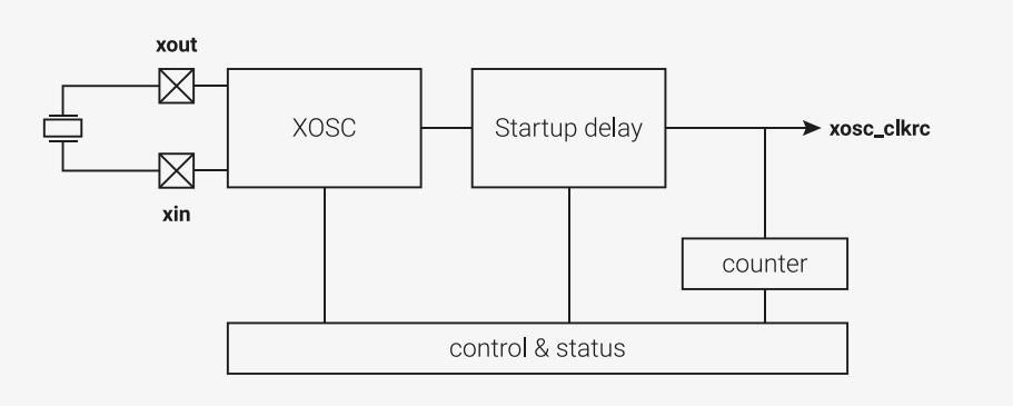
The Crystal Oscillator (XOSC) uses an external crystal to produce an accurate reference clock. RP2350 supports 1 MHz to 50 MHz crystals and the RP2350 reference design (see Hardware design with RP2350, Minimal Design Example ) uses a 12 MHz crystal. The reference clock is distributed to the PLLs, which can be used to multiply the XOSC frequency to provide accurate high speed clocks. For example, they can generate a 48 MHz clock which meets the frequency accuracy requirement of the USB interface and a 150 MHz maximum speed system clock. The XOSC clock is also a clock source for the clock generators and can be used directly if required.
If the user already has an accurate clock source, it is possible to drive an external clock directly into XIN (aka XI), and disable the oscillator circuit. In this mode XIN can be driven at up to 50 MHz.
To use XOSC clock externally, output it to a GPIO pin using one of the
clk_gpclk0-clk_gpclk3
generators. You cannot take XOSC output directly from the XIN (XI) or XOUT (XO) pins.
NOTE
A minimum crystal frequency of 5 MHz is needed for the PLL. See Section 8.6, "PLL" .
8.2.1.1. Recommended crystals
For the best performance and stability across typical operating temperature ranges, it is recommended to use the Abracon ABM8-272-T3. You can source the ABM8-272-T3 directly from Abracon or from an authorised reseller. The Abracon ABM8-272-T3 has the following specifications:
Table 597. Key Crystal Specifications.
| Parameters | Minimum | Typical | Maximum | Units | Notes |
|---|---|---|---|---|---|
| Center Frequency | 12.000 | 12.000 | 12.000 | MHz | |
| Operation Mode | Fundamental-AT | Fundamental-AT | Fundamental-AT | ||
| Operating Temperature | -40 | +85 | °C | ||
| Storage Temperature | -55 | +125 | °C | ||
| Frequency Tolerance (25 °C) | -30 | +30 | ppm | ||
| Frequency Stability (25 °C) | -30 | +30 | ppm | ||
| Equivalent Series Resistance (R1) | 50 | Ω | |||
| Shunt Capacitance (C0) | 3.0 | pF | |||
| Load Capacitance (CL) | 10 | 10 | 10 | pF | |
| Drive Level | 10 | 200 | μW | ||
| Aging | -5 | +5 | ppm | @25±3 °C, 1st year | |
| Insulation Resistance | 500 | MΩ | @100 Vdc±15 V |
Even if you use a crystal with similar specifications, you will need to test the circuit over a range of temperatures to
ensure stability.
The crystal oscillator is powered from the VDDIO voltage. As a result, the Abracon crystal and that particular damping resistor are tuned for 3.3V operation. If you use a different IO voltage, you will need to re-tune.
Any changes to crystal parameters risk instability across any components connected to the crystal circuit.
If you can't source the recommended crystal directly from Abracon or a reseller, contact applications@raspberrypi.com .
Raspberry Pi Pico 2 has been specifically tuned for the specifications of the Abracon ABM8-272-T3 crystal. For an example of how to use a crystal with RP2350, see the Raspberry Pi Pico 2 board schematic in Appendix B of Raspberry Pi Pico 2 Datasheet and the Raspberry Pi Pico 2 design files .
8.2.2. Changes from RP2040
- Maximum crystal frequency increased from 15 MHz to 50 MHz, when appropriate range is selected in
CTRL.FREQ_RANGE
NOTE
The above change applies when using the XOSC as a crystal oscillator, with a crystal connected between the
XIN
and
XOUT
pins. When using the XOSC
XIN
pin as a CMOS clock input from an external oscillator, the maximum is always 50 MHz. You do not have to configure
CTRL.FREQ_RANGE
for the CMOS input case. The CMOS input behaviour is the same as RP2040.
NOTE
The maximum
clk_ref
frequency is 25 MHz. If you use a >25 MHz crystal as the source of
clk_ref
, you must divide the XOSC output using the
clk_ref
divider.
8.2.3. Usage
The XOSC is disabled on chip startup and RP2350 boots using the Ring Oscillator (ROSC). To start the XOSC, the programmer must set the
CTRL_ENABLE
register. The XOSC is not immediately usable because it takes time for the oscillations to build to sufficient amplitude. This time will be dependent on the chosen crystal but will be of the order of a few milliseconds. The XOSC incorporates a timer controlled by the
STARTUP_DELAY
register to automatically manage this, which sets a flag (
STATUS_STABLE
) when the XOSC clock is usable.
8.2.4. Startup delay
The
STARTUP_DELAY
register specifies how many clock cycles must be seen from the crystal before it can be used. This is specified in multiples of 256. The SDK
xosc_init
function sets this value. The 1 ms default is sufficient for the RP2350 reference design (see
Hardware design with RP2350, Minimal Design Example
) which runs the XOSC at 12 MHz. When the timer expires, the
STATUS_STABLE
flag will be set to indicate the XOSC output can be used.
Before starting the XOSC the programmer must ensure the
STARTUP_DELAY
register is correctly configured. The required value can be calculated by:
So with a 12 MHz crystal and a 1 ms wait time, the calculation is:
The value is rounded up to the nearest integer, so the wait time will be just over 1 ms.
8.2.5. XOSC counter
The COUNT register provides a method of managing short software delays. To use this method:
- 1. Write a value to the COUNT register. The register automatically begins to count down to zero at the XOSC frequency.
- 2. Poll the register until it reaches zero.
This is preferable to using NOPs in software loops because it is independent of the core clock frequency, the compiler, and the execution time of the compiled code.
8.2.6. DORMANT mode
In DORMANT mode (see Section 6.5.3, “DORMANT state” ), all of the on-chip clocks can be paused to save power. This is particularly useful in battery-powered applications. RP2350 wakes from DORMANT mode by interrupt: either from an external event, such as an edge on a GPIO pin, or from the AON Timer. This must be configured before entering DORMANT mode. To use the AON Timer to trigger a wake from DORMANT mode, it must be clocked from the LPOSC or from an external source.
To enter DORMANT mode:
- 1. Switch all internal clocks to be driven from XOSC or ROSC and stop the PLLs.
- 2. Choose an oscillator (XOSC or ROSC). Write a specific 32-bit value to the DORMANT register of the chosen oscillator to stop it.
When exiting DORMANT mode, the chosen oscillator will restart. If you chose XOSC, the frequency will be more precise, but the restart will take more time due to startup delay (>1 ms on the RP2350 reference design (see Hardware design with RP2350, Minimal Design Example )). If you chose ROSC, the frequency will be less precise, but the start-up time is very short (approximately 1µs). See Section 6.5.3.1, “Waking from the DORMANT state” for the events which cause the system to exit DORMANT mode.
NOTEYou must stop the PLLs before entering DORMANT mode.
SDK: https://github.com/raspberrypi/pico-sdk/blob/master/src/rp2_common/hardware_xosc/xosc.c Lines 56 - 63
56 void xosc_dormant(void) {
57     // WARNING: This stops the xosc until woken up by an irq
58     xosc_hw->dormant = XOSC_DORMANT_VALUE_DORMANT;
59     // Wait for it to become stable once woken up
60     while(!(xosc_hw->status & XOSC_STATUS_STABLE_BITS)) {
61         tight_loop_contents();
62     }
63 }
⚠ WARNING
If you do not configure IRQ before entering DORMANT mode, neither oscillator will restart.
See Section 6.5.6.2, “DORMANT” for a complete example of DORMANT mode using the XOSC.
8.2.7. Programmer’s model
SDK: https://github.com/raspberrypi/pico-sdk/blob/master/src/rp2350/hardware_structs/include/hardware/structs/xosc.h Lines 27 - 57
27 typedef struct {
28     _REG_(XOSC_CTRL_OFFSET) // XOSC_CTRL
29     // Crystal Oscillator Control
30     // 0x00fff000 [23:12] ENABLE      (-) On power-up this field is initialised to DISABLE and
    the...
31     // 0x00000fff [11:0]  FREQ_RANGE  (-) The 12-bit code is intended to give some
    protection...
32     io_rw_32 ctrl;
33
34     _REG_(XOSC_STATUS_OFFSET) // XOSC_STATUS
35     // Crystal Oscillator Status
36     // 0x80000000 [31]   STABLE      (0) Oscillator is running and stable
37     // 0x01000000 [24]   BADWRITE    (0) An invalid value has been written to CTRL_ENABLE
    or...
38     // 0x00010000 [12]   ENABLED     (-) Oscillator is enabled but not necessarily running
    and...
39     // 0x00000003 [1:0]  FREQ_RANGE  (-) The current frequency range setting
40     io_rw_32 status;
41
42     _REG_(XOSC_DORMANT_OFFSET) // XOSC_DORMANT
43     // Crystal Oscillator pause control
44     // 0xffffffff [31:0] DORMANT     (-) This is used to save power by pausing the XOSC +
45     io_rw_32 dormant;
46
47     _REG_(XOSC_STARTUP_OFFSET) // XOSC_STARTUP
48     // Controls the startup delay
49     // 0x00100000 [20]   X4          (-) Multiplies the startup_delay by 4, just in case
50     // 0x00003fff [13:0] DELAY      (-) in multiples of 256*xtal_period
51     io_rw_32 startup;
52
53     _REG_(XOSC_COUNT_OFFSET) // XOSC_COUNT
54     // A down counter running at the XOSC frequency which counts to zero and stops.
55     // 0x0000ffff [15:0] COUNT      (0x0000)
56     io_rw_32 count;
57 } xosc_hw_t;
SDK: https://github.com/raspberrypi/pico-sdk/blob/master/src/rp2_common/hardware_xosc/xosc.c Lines 29 - 43
29 void xosc_init(void) {
30     // Assumes 1-15 MHz input, checked above.
31     xosc_hw->ctrl = XOSC_CTRL_FREQ_RANGE_VALUE_1_15MHZ;
32
33     // Set xosc startup delay
34     xosc_hw->startup = STARTUP_DELAY;
35
36     // Set the enable bit now that we have set freq range and startup delay
37     hw_set_bits(&xosc_hw->ctrl, XOSC_CTRL_ENABLE_VALUE_ENABLE << XOSC_CTRL_ENABLE_LSB);
38
39 // Wait for XOSC to be stable
40 while(!(xosc_hw->status & XOSC_STATUS_STABLE_BITS)) {
41     tight_loop_contents();
42 }
43 }
8.2.8. List of registers
The XOSC registers start at a base address of 0x40048000 (defined as XOSC_BASE in SDK).
Table 598. List of XOSC registers
| Offset | Name | Info |
|---|---|---|
| 0x00 | CTRL | Crystal Oscillator Control |
| 0x04 | STATUS | Crystal Oscillator Status |
| 0x08 | DORMANT | Crystal Oscillator pause control |
| 0x0c | STARTUP | Controls the startup delay |
| 0x10 | COUNT | A down counter running at the XOSC frequency which counts to zero and stops. |
XOSC: CTRL Register
Offset: 0x00
Description
Crystal Oscillator Control
Table 599. CTRL Register
| Bits | Description | Type | Reset |
|---|---|---|---|
| 31:24 | Reserved. | - | - |
| 23:12 | ENABLE:
On power-up this field is initialised to DISABLE and the chip runs from the ROSC. If the chip has subsequently been programmed to run from the XOSC then setting this field to DISABLE may lock-up the chip. If this is a concern then run the clk_ref from the ROSC and enable the clk_sys RESUS feature. The 12-bit code is intended to give some protection against accidental writes. An invalid setting will retain the previous value. The actual value being used can be read from STATUS_ENABLED | RW | - |
| Enumerated values: | |||
| 0xd1e → DISABLE | |||
| 0xfab → ENABLE | |||
| 11:0 | FREQ_RANGE: The 12-bit code is intended to give some protection against accidental writes. An invalid setting will retain the previous value. The actual value being used can be read from STATUS_FREQ_RANGE | RW | - |
| Enumerated values: | |||
| 0xaa0 → 1_15MHZ | |||
| 0xaa1 → 10_30MHZ | |||
| 0xaa2 → 25_60MHZ | |||
| 0xaa3 → 40_100MHZ |
XOSC: STATUS Register
Offset: 0x04
Description
Crystal Oscillator Status
Table 600. STATUS Register
| Bits | Description | Type | Reset |
|---|---|---|---|
| 31 | STABLE : Oscillator is running and stable | RO | 0x0 |
| 30:25 | Reserved. | - | - |
| 24 | BADWRITE : An invalid value has been written to CTRL_ENABLE or CTRL_FREQ_RANGE or DORMANT | WC | 0x0 |
| 23:13 | Reserved. | - | - |
| 12 | ENABLED : Oscillator is enabled but not necessarily running and stable, resets to 0 | RO | - |
| 11:2 | Reserved. | - | - |
| 1:0 | FREQ_RANGE : The current frequency range setting | RO | - |
| Enumerated values: | |||
| 0x0 → 1_15MHZ | |||
| 0x1 → 10_30MHZ | |||
| 0x2 → 25_60MHZ | |||
| 0x3 → 40_100MHZ |
XOSC: DORMANT Register
Offset: 0x08
Description
Crystal Oscillator pause control
Table 601. DORMANT Register
| Bits | Description | Type | Reset |
|---|---|---|---|
| 31:0 | This is used to save power by pausing the XOSC On power-up this field is initialised to WAKE An invalid write will also select WAKE WARNING: stop the PLLs before selecting dormant mode WARNING: setup the irq before selecting dormant mode | RW | - |
| Enumerated values: | |||
| 0x636f6d61 → DORMANT | |||
| 0x77616b65 → WAKE |
XOSC: STARTUP Register
Offset: 0x0c
Description
Controls the startup delay
Table 602. STARTUP Register
| Bits | Description | Type | Reset |
|---|---|---|---|
| 31:21 | Reserved. | - | - |
| Bits | Description | Type | Reset |
|---|---|---|---|
| 20 | X4 : Multiplies the startup_delay by 4, just in case. The reset value is controlled by a mask-programmable tiecell and is provided in case we are booting from XOSC and the default startup delay is insufficient | RW | 0x0 |
| 19:14 | Reserved. | - | - |
| 13:0 | DELAY : in multiples of 256*xtal_period. The reset value of 0xc4 corresponds to approx 50 000 cycles. | RW | 0x00c4 |
XOSC: COUNT Register
Offset: 0x10
Table 603. COUNT Register
| Bits | Description | Type | Reset |
|---|---|---|---|
| 31:16 | Reserved. | - | - |
| 15:0 | A down counter running at the xosc frequency which counts to zero and stops. Can be used for short software pauses when setting up time sensitive hardware. To start the counter, write a non-zero value. Reads will return 1 while the count is running and 0 when it has finished. Minimum count value is 4. Count values <4 will be treated as count value =4. Note that synchronisation to the register clock domain costs 2 register clock cycles and the counter cannot compensate for that. | RW | 0x0000 |
8.3. Ring oscillator (ROSC)
8.3.1. Overview
The Ring Oscillator (ROSC) is an on-chip oscillator built from a ring of inverters. It requires no external components and is started automatically during RP2350 power up. It provides the clock to the cores during boot. The frequency of the ROSC is programmable and it can directly provide a high speed clock to the cores, but the frequency varies with Process, Voltage, and Temperature (PVT) so it cannot provide clocks for components that require an accurate frequency such as the AON Timer, USB, and ADC. The frequency can be randomised to provide some protection against attempts to recover the system clock from power traces. Methods for mitigating unwanted frequency variation are discussed in Section 8.1, “Overview” , but these are only relevant to very low power designs. For most applications requiring accurate clock frequencies, switch to the XOSC and PLLs. During boot, the ROSC runs at a nominal 11MHz and is guaranteed to be in the range 4.6MHz to 19.6MHz without randomisation and 4.6MHz to 24.0MHz with randomisation.
i NOTE
RP2350 A3 and later enable randomisation by default, and the bootrom quadruples the ROSC base frequency by reducing
DIV
to 2. As a result,
clk_sys
is guaranteed to range between 18.4 MHz and 96.0 MHz.
clk_ref
is maintained at a nominal 11 MHz by increasing its divisor. This change increases the sensitivity of the glitch detectors, which have an inverse relationship with clock period, consequently better protecting the ROM’s early boot paths.
After the chip has booted, the programmer can choose to continue running from the ROSC and increase its frequency or start the Crystal Oscillator (XOSC) and PLLs. You can disable the ROSC when you’ve switched the system clocks to the XOSC. Each oscillator has advantages; switch between them to achieve the best solution for your application.
Figure 39. ROSC overview.
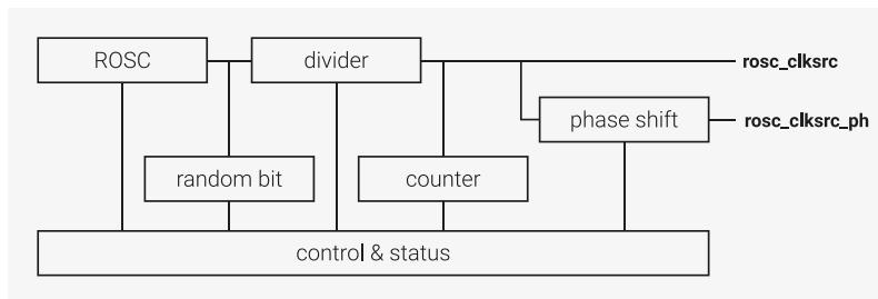
graph TD
    ROSC[ROSC] --- Div[divisor]
    Div --- Random[random bit]
    Div --- Counter[counter]
    Counter --- Phase[phase shift]
    Phase --- ROSC_Clksrc[rosc_clksrc]
    Phase --- ROSC_Clksrc_ph[rosc_clksrc_ph]
    Div --- CS[control & status]
    Random --- CS
    Counter --- CS
    Phase --- CS
    ROSC --- CS
8.3.2. Changes from RP2040
Frequency randomisation feature added.
8.3.3. Changes between RP2350 revisions
RP2350 A3 changes the reset values of FREQA.DS0_RANDOM and FREQA.DS1_RANDOM from 0 to 1. See Hardware changes for information about related changes made to the clock configuration at reset. See Bootrom changes for related changes made in the A3 boot ROM.
8.3.4. ROSC/XOSC trade-offs
The ROSC has several advantages:
- • Flexibility due to programmable frequency
- • Low power requirements
- • No need for internal or external components
- • Optional frequency randomisation improves security
Because the ROSC has programmable frequency, it can provide a fast core clock without starting the PLLs and can generate slower peripheral clocks by dividing by clock generators ( Section 8.1, “Overview” ). The ROSC starts immediately and responds immediately to frequency controls. It retains the frequency setting when entering and exiting the DORMANT state (see Section 6.5.3, “DORMANT state” ). However, the user must be aware that the frequency may have drifted when exiting the DORMANT state due to changes in the supply voltage and the chip temperature.
The disadvantage of the ROSC is its frequency variation with PVT (Process, Voltage, and Temperature), which makes it unsuitable for generating precise clocks or for applications where software execution timing is important. However, the PVT frequency variation can be exploited to provide automatic frequency scaling to maximise performance. This is discussed in Section 8.1, “Overview” .
The only advantage of the XOSC is its accurate frequency, but this is an overriding requirement in many applications.
The XOSC has the following disadvantages:
- • the requirement for external components (a crystal, etc.)
- • higher power consumption
- • slow startup time (>1ms)
- • fixed, low frequency
PLLs are required to produce higher-frequency clocks. They consume more power and take significant time to start up or change frequency. Exiting DORMANT mode is much slower than for ROSC because the XOSC must restart and the PLLs must be reconfigured.
8.3.5. Modifying the frequency
The ROSC is arranged as 8 stages, each with programmable drive. The ROSC provides two methods of controlling the frequency. The frequency range controls the number of stages in the ROSC loop and the
FREQA
&
FREQB
registers control the drive strength of the stages.
To change the frequency range, write to the
FREQ_RANGE
register, which controls the number of stages in the ROSC loop. The
FREQ_RANGE
register supports the following configurations:
Table 604. ROSC stage ranges
| Name | Number of stages | Range (stages) |
|---|---|---|
| LOW | 8 | 0-7 |
| MEDIUM | 6 | 2-7 |
| HIGH | 4 | 4-7 |
| TOOHIGH | 2 | 6-7 |
Change
FREQ_RANGE
one step at a time until you reach the desired range. When increasing the frequency range, ROSC output will not glitch, so the output clock can continue to be used. When decreasing the frequency range, ROSC output
will
glitch, so you must select an alternate clock source for the modules clocked by ROSC or hold them in reset during the transition.
The behaviour has not been fully characterised, but the
MEDIUM
range will be approximately 1.33 times the
LOW
range, the
HIGH
range will be 2 times the
LOW
range and the
TOOHIGH
range will be 4 times the
LOW
range. The
TOOHIGH
range is aptly named. It should not be used because the internal logic of the ROSC will not run at that frequency.
The
FREQA
and
FREQB
registers control the drive strength of the stages in the ROSC loop. As the drive strength increases, the delay through the stage decreases and the oscillation frequency increases. Each stage has 3 drive strength control bits. Each bit turns on an additional drive, therefore each stage has 4 drive strength settings equal to the number of bits set, with 0 being the default, 1 being double drive, 2 being triple drive and 3 being quadruple drive. Extra drives do not have a linear effect on frequency: the second has less impact than the first, the third has less impact than the second, and so on. To ensure smooth transitions, change one drive strength bit at a time. When
FREQ_RANGE
shortens the ROSC loop, the bypassed stages still propagate the signal and therefore their drive strengths must be set to at least the same level as the lowest drive strength in the stages that are in the loop. This will not affect the oscillation frequency.
8.3.6. Randomising the frequency
Randomisation is enabled by setting the drive strength controls for the first two stages of the ROSC loop to
DS0_RANDOM
and
DS1_RANDOM
. An LFSR then provides the drive strength controls for those two stages which are always included in the loop regardless of the
FREQ_RANGE
setting. It is recommended to randomise both stages. When the low
FREQ_RANGE
is selected the randomiser will increase the frequency by up to 22% of the default. The increase will be approximately half of that if only one stage is randomised. The LFSR can be seeded by writing to the
RANDOM
register. This can be done at any time but will restart the randomiser.
8.3.7. ROSC divider
The ROSC frequency is too fast to be used directly, so it is divided in an integer divider controlled by the
DIV
register. You can change
DIV
while the ROSC is running, and the output clock will change frequency without glitching. The default divisor is 8, which ensures the output clock is in the specified range on chip startup.
The divider has two outputs,
rosc_clksrc
and
rosc_clksrc_ph
.
rosc_clksrc_ph
is a phase shifted version of
rosc_clksrc
. This is primarily intended for use during product development; the outputs are identical if the
PHASE
register is left in its default state.
8.3.8. Random number generator
When the system clocks are running from the XOSC, you can use the ROSC to generate random numbers. Enable the ROSC and read the
RANDOMBIT
register to get a 1-bit random number; to get an
n
-bit value, read it
n
times. This does not meet the requirements of randomness for security systems because it can be compromised, but it may be useful in less critical applications. If the cores are running from the ROSC, the value will not be random because the timing of the register read will be correlated to the phase of the ROSC.
8.3.9. ROSC counter
The
COUNT
register provides a method of managing short software delays. To use this method:
- 1. Write a value to the
COUNTregister. The register automatically begins to count down to zero at the ROSC frequency. - 2. Poll the register until it reaches zero.
This is preferable to using NOPs in software loops because it is independent of the core clock frequency, the compiler, and the execution time of the compiled code.
8.3.10. DORMANT mode
In DORMANT mode (see Section 6.5.3, “DORMANT state” ), all of the on-chip clocks can be paused to save power. This is particularly useful in battery-powered applications. RP2350 wakes from DORMANT mode by interrupt: either from an external event, such as an edge on a GPIO pin, or from the AON Timer. This must be configured before entering DORMANT mode. To use the AON Timer to trigger a wake from DORMANT mode, it must be clocked from the LPOSC or from an external source.
To enter DORMANT mode:
- 1. Switch all internal clocks to be driven from XOSC or ROSC and stop the PLLs.
- 2. Choose an oscillator (XOSC or ROSC). Write a specific 32-bit value to the
DORMANTregister of the chosen oscillator to stop it.
When exiting DORMANT mode, the chosen oscillator will restart. If you chose XOSC, the frequency will be more precise, but the restart will take more time due to startup delay (>1ms on the RP2350 reference design (see Hardware design with RP2350, Minimal Design Example )). If you chose ROSC, the frequency will be less precise, but the start-up time is very short (approximately 1µs). See Section 6.5.3.1, “Waking from the DORMANT state” for the events which cause the system to exit DORMANT mode.
i NOTE
You must stop the PLLs before entering DORMANT mode.
Pico Extras: https://github.com/raspberrypi/pico-extras/blob/master/src/rp2_common/hardware_rosc/rosc.c Lines 56 - 61
56 void rosc_set_dormant(void) {
57 // WARNING: This stops the rosc until woken up by an irq
58 rosc_write(&rosc_hw->dormant, ROSC_DORMANT_VALUE_DORMANT);
59 // Wait for it to become stable once woken up
60 while(!(rosc_hw->status & ROSC_STATUS_STABLE_BITS));
61 } WARNING
If you do not configure IRQ before entering DORMANT mode, neither oscillator will restart.
See Section 6.5.6.2, “DORMANT” for a some examples of dormant mode.
8.3.11. List of registers
The ROSC registers start at a base address of
0x400e8000
(defined as
ROSC_BASE
in SDK).
Table 605. List of ROSC registers
| Offset | Name | Info |
|---|---|---|
| 0x00 | CTRL | Ring Oscillator control |
| 0x04 | FREQA | Ring Oscillator frequency control A |
| 0x08 | FREQB | Ring Oscillator frequency control B |
| 0x0c | RANDOM | Loads a value to the LFSR randomiser |
| 0x10 | DORMANT | Ring Oscillator pause control |
| 0x14 | DIV | Controls the output divider |
| 0x18 | PHASE | Controls the phase shifted output |
| 0x1c | STATUS | Ring Oscillator Status |
| 0x20 | RANDOMBIT | Returns a 1 bit random value |
| 0x24 | COUNT | A down counter running at the ROSC frequency which counts to zero and stops. |
ROSC: CTRL Register
Offset: 0x00
Description
Ring Oscillator control
Table 606. CTRL Register
| Bits | Description | Type | Reset |
|---|---|---|---|
| 31:24 | Reserved. | - | - |
| 23:12 | ENABLE:
On power-up this field is initialised to ENABLE The system clock must be switched to another source before setting this field to DISABLE otherwise the chip will lock up The 12-bit code is intended to give some protection against accidental writes. An invalid setting will enable the oscillator. | RW | - |
| Enumerated values: | |||
| 0xd1e → DISABLE | |||
| 0xfab → ENABLE |
| Bits | Description | Type | Reset |
|---|---|---|---|
| 11:0 | FREQ_RANGE
: Controls the number of delay stages in the ROSC ring LOW uses stages 0 to 7 MEDIUM uses stages 0 to 5 HIGH uses stages 0 to 3 TOOHIGH uses stages 0 to 1 and should not be used because its frequency exceeds design specifications The clock output will not glitch when changing the range up one step at a time The clock output will glitch when changing the range down Note: the values here are gray coded which is why HIGH comes before TOOHIGH | RW | 0xaa0 |
| Enumerated values: | |||
| 0xfa4 → LOW | |||
| 0xfa5 → MEDIUM | |||
| 0xfa7 → HIGH | |||
| 0xfa6 → TOOHIGH |
ROSC: FREQA Register
Offset: 0x04
Description
The FREQA & FREQB registers control the frequency by controlling the drive strength of each stage
The drive strength has 4 levels determined by the number of bits set
Increasing the number of bits set increases the drive strength and increases the oscillation frequency
0 bits set is the default drive strength
1 bit set doubles the drive strength
2 bits set triples drive strength
3 bits set quadruples drive strength
For frequency randomisation set both DS0_RANDOM=1 & DS1_RANDOM=1
Table 607. FREQA Register
| Bits | Description | Type | Reset |
|---|---|---|---|
| 31:16 | PASSWD
: Set to 0x9696 to apply the settings Any other value in this field will set all drive strengths to 0 | RW | 0x0000 |
| Enumerated values: | |||
| 0x9696 → PASS | |||
| 15 | Reserved. | - | - |
| 14:12 | DS3 : Stage 3 drive strength | RW | 0x0 |
| 11 | Reserved. | - | - |
| 10:8 | DS2 : Stage 2 drive strength | RW | 0x0 |
| 7 | DS1_RANDOM : Randomises the stage 1 drive strength | RW | 0x1 |
| 6:4 | DS1 : Stage 1 drive strength | RW | 0x0 |
| 3 | DS0_RANDOM : Randomises the stage 0 drive strength | RW | 0x1 |
| 2:0 | DS0 : Stage 0 drive strength | RW | 0x0 |
ROSC: FREQB Register
Offset: 0x08
DescriptionFor a detailed description see freqa register
Table 608. FREQB Register
| Bits | Description | Type | Reset |
|---|---|---|---|
| 31:16 | PASSWD
: Set to 0x9696 to apply the settings Any other value in this field will set all drive strengths to 0 | RW | 0x0000 |
| Enumerated values: | |||
| 0x9696 → PASS | |||
| 15 | Reserved. | - | - |
| 14:12 | DS7 : Stage 7 drive strength | RW | 0x0 |
| 11 | Reserved. | - | - |
| 10:8 | DS6 : Stage 6 drive strength | RW | 0x0 |
| 7 | Reserved. | - | - |
| 6:4 | DS5 : Stage 5 drive strength | RW | 0x0 |
| 3 | Reserved. | - | - |
| 2:0 | DS4 : Stage 4 drive strength | RW | 0x0 |
Offset: 0x0c
DescriptionLoads a value to the LFSR randomiser
Table 609. RANDOM Register
| Bits | Description | Type | Reset |
|---|---|---|---|
| 31:0 | SEED | RW | 0x3f04b16d |
Offset: 0x10
DescriptionRing Oscillator pause control
Table 610. DORMANT Register
| Bits | Description | Type | Reset |
|---|---|---|---|
| 31:0 | This is used to save power by pausing the ROSC On power-up this field is initialised to WAKE An invalid write will also select WAKE Warning: setup the irq before selecting dormant mode | RW | - |
| Enumerated values: | |||
| 0x636f6d61 → DORMANT | |||
| 0x77616b65 → WAKE |
Offset: 0x14
DescriptionControls the output divider
Table 611. DIV Register
| Bits | Description | Type | Reset |
|---|---|---|---|
| 31:16 | Reserved. | - | - |
| 15:0 | set to 0xaa00 + div where div = 0 divides by 128 div = 1-127 divides by div any other value sets div=128 this register resets to div=32 | RW | - |
| Enumerated values: | |||
| 0xaa00 → PASS |
ROSC: PHASE Register
Offset: 0x18
Description
Controls the phase shifted output
Table 612. PHASE Register
| Bits | Description | Type | Reset |
|---|---|---|---|
| 31:12 | Reserved. | - | - |
| 11:4 | PASSWD
: set to 0xaa any other value enables the output with shift=0 | RW | 0x00 |
| 3 | ENABLE
: enable the phase-shifted output this can be changed on-the-fly | RW | 0x1 |
| 2 | FLIP
: invert the phase-shifted output this is ignored when div=1 | RW | 0x0 |
| 1:0 | SHIFT
: phase shift the phase-shifted output by SHIFT input clocks this can be changed on-the-fly must be set to 0 before setting div=1 | RW | 0x0 |
ROSC: STATUS Register
Offset: 0x1c
Description
Ring Oscillator Status
Table 613. STATUS Register
| Bits | Description | Type | Reset |
|---|---|---|---|
| 31 | STABLE : Oscillator is running and stable | RO | 0x0 |
| 30:25 | Reserved. | - | - |
| 24 | BADWRITE : An invalid value has been written to CTRL_ENABLE or CTRL_FREQ_RANGE or FREQA or FREQB or DIV or PHASE or DORMANT | WC | 0x0 |
| 23:17 | Reserved. | - | - |
| 16 | DIV_RUNNING
: post-divider is running this resets to 0 but transitions to 1 during chip startup | RO | - |
| 15:13 | Reserved. | - | - |
| 12 | ENABLED
: Oscillator is enabled but not necessarily running and stable this resets to 0 but transitions to 1 during chip startup | RO | - |
| 11:0 | Reserved. | - | - |
ROSC: RANDOMBIT Register
Offset: 0x20
Table 614.
RANDOMBIT Register
| Bits | Description | Type | Reset |
|---|---|---|---|
| 31:1 | Reserved. | - | - |
| 0 | This just reads the state of the oscillator output so randomness is compromised if the ring oscillator is stopped or run at a harmonic of the bus frequency | RO | 0x1 |
ROSC: COUNT Register
Offset: 0x24
Table 615. COUNT
Register
| Bits | Description | Type | Reset |
|---|---|---|---|
| 31:16 | Reserved. | - | - |
| 15:0 | A down counter running at the ROSC frequency which counts to zero and stops. To start the counter write a non-zero value. Can be used for short software pauses when setting up time sensitive hardware. | RW | 0x0000 |
8.4. Low Power oscillator (LPOSC)
The Low Power Oscillator (LPOSC) provides a clock signal to the always-on logic when the main crystal oscillator is powered down in a low power (P1.x) state. It operates at a nominal 32.768kHz and is an RC oscillator, requiring no external components. The oscillator’s output clock is used to sequence initial chip start up and transition to and from low-power states. It can also be used by the AON Timer, see Section 12.10, “Always-on timer” .
The oscillator starts up as soon as the core power supply is available and power-on reset has been released. If brownout detection is enabled, the oscillator will be disabled when a core supply brownout is detected, but will restart as soon as the core supply has recovered and brownout reset has been released. The oscillator’s frequency takes around 1ms to stabilise, and the chip will be held in reset during this period.
8.4.1. Frequency accuracy and calibration
The low power oscillator has an initial frequency accuracy of \( \pm 20\% \) . However, it can be trimmed to \( \pm 1.5\% \) using the TRIM field in the LPOSC register. 63 trim steps are available, each between 1% and 3% of the oscillator’s initial frequency. The frequency can be trimmed down by 32 steps or up by 31 steps. See Table 616, “low power oscillator output frequency and trimming” and Section 8.4.3, “List of registers” for details.
Table 616. low power
oscillator output
frequency and
trimming
| Parameter | Description | Min | Typ | Max | Units |
|---|---|---|---|---|---|
| F 0.initial | initial output frequency | 26.2144 | 32.768 | 39.3216 | kHz |
| trim STEP | frequency trim step | - | 1 | 3 | % of initial output frequency |
| F 0.trimmed | trimmed output frequency | 32.27648 | 32.768 | 33.25952 | kHz |
Frequency drift with temperature: \( \pm 14\% \) .
Frequency drift with power supply voltage: \( \pm 20\% \) .
8.4.2. Using an external low-power clock
Instead of using the low-power RC oscillator, an external 32.768 kHz low power clock signal can be provided on one of GPIO 12, 14, 20, or 22. Alternatively, those GPIOs can be used to provide a 1 kHz or 1 Hz tick. See Section 12.10.5.2, “Using an external clock in place of LPOSC” and Section 12.10.7, “Using an external clock or tick from GPIO” for more details.
8.4.3. List of registers
The low power oscillator shares register address space with other power management subsystems in the always-on domain. The address space is referred to as POWMAN elsewhere in this document. A complete list of POWMAN registers is provided in Section 6.4, “Power management (POWMAN) registers” , but information on registers associated with the low power oscillator is repeated here.
The POWMAN registers start at a base address of
0x40100000
(defined as
POWMAN_BASE
in SDK).
8.5. Tick generators
8.5.1. Overview
The tick generators provide time references for several blocks:
- • System timers: TIMER0 and TIMER1 ( Section 12.8, “System timers” )
- • RISC-V platform timer ( Section 3.1.8, “RISC-V platform timer” )
- • Arm Cortex-M33 SysTick timers for core 0 and core 1
- • The watchdog timer ( Section 12.9, “Watchdog” )
A tick is a periodic signal which provides a timebase for a timer or counter. These signals are similar to clocks, although they do not drive the clock inputs of any registers on the chip. The use of ticks as opposed to clocks makes it simpler to distribute timebase information that is independent of any subsystem clocks. For example, the system timers (TIMER0 and TIMER1) should continue to count once per microsecond even as the system clock varies according to processor demand.
The tick generators use
clk_ref
as their reference clock (see
Section 8.1, “Overview”
for an overview of system-level clocks including
clk_ref
). Ideally,
clk_ref
will be configured to use the crystal oscillator (
Section 8.2, “Crystal oscillator (XOSC)”
) to provide an accurate reference. The generators divide
clk_ref
internally to generate a tick signal for each destination.
The SDK expects a nominal 1
\(
\mu
\)
s timebase for the system timers and the RISC-V platform timer. Similarly the Cortex-M33 SysTick timers require a 1
\(
\mu
\)
s timebase to match the hardwired value of 100,000 in the
SYST_CALIB
register, which standard Arm software uses to scale SysTick delays. However, you may need to scale these timebases differently if your software has specific requirements such as a longer maximum delay on the 24-bit SysTick peripherals. The tick generator can scale each destination’s tick timebase independently of the others.
For a 12 MHz reference clock, set the cycle count to 12 to generate a 1 \( \mu \) s tick. A 1 MHz clock has a period of 1 \( \mu \) s, so
the hardware needs to count for 12 times as many clock cycles to get a 1 \( \mu \) s tick from a reference running at 12 \( \times \) 1 MHz.
Before changing the cycle count, always stop the tick generator with the
TIMER0_CTRL.ENABLE
bit. You can re-enable once the tick generator is configured.
8.5.2. List of registers
The tick generator registers start at a base address of
0x40108000
(defined as
TICKS_BASE
in SDK).
Table 617. List of TICKS registers
| Offset | Name | Info |
|---|---|---|
| 0x00 | PROC0_CTRL | Controls the tick generator |
| 0x04 | PROC0_CYCLES | |
| 0x08 | PROC0_COUNT | |
| 0x0c | PROC1_CTRL | Controls the tick generator |
| 0x10 | PROC1_CYCLES | |
| 0x14 | PROC1_COUNT | |
| 0x18 | TIMER0_CTRL | Controls the tick generator |
| 0x1c | TIMER0_CYCLES | |
| 0x20 | TIMER0_COUNT | |
| 0x24 | TIMER1_CTRL | Controls the tick generator |
| 0x28 | TIMER1_CYCLES | |
| 0x2c | TIMER1_COUNT | |
| 0x30 | WATCHDOG_CTRL | Controls the tick generator |
| 0x34 | WATCHDOG_CYCLES | |
| 0x38 | WATCHDOG_COUNT | |
| 0x3c | RISCV_CTRL | Controls the tick generator |
| 0x40 | RISCV_CYCLES | |
| 0x44 | RISCV_COUNT |
TICKS: PROC0_CTRL Register
Offset: 0x00
Description
Controls the tick generator
Table 618. PROC0_CTRL Register
| Bits | Description | Type | Reset |
|---|---|---|---|
| 31:2 | Reserved. | - | - |
| 1 | RUNNING : Is the tick generator running? | RO | - |
| 0 | ENABLE : start / stop tick generation | RW | 0x0 |
TICKS: PROC0_CYCLES Register
Offset: 0x04
Table 619.
PROC0_CYCLES
Register
| Bits | Description | Type | Reset |
|---|---|---|---|
| 31:9 | Reserved. | - | - |
| 8:0 | Total number of clk_tick cycles before the next tick. | RW | 0x000 |
TICKS: PROC0_COUNT Register
Offset: 0x08
Table 620.
PROC0_COUNT
Register
| Bits | Description | Type | Reset |
|---|---|---|---|
| 31:9 | Reserved. | - | - |
| 8:0 | Count down timer: the remaining number clk_tick cycles before the next tick is generated. | RO | - |
TICKS: PROC1_CTRL Register
Offset: 0x0c
Description
Controls the tick generator
Table 621.
PROC1_CTRL Register
| Bits | Description | Type | Reset |
|---|---|---|---|
| 31:2 | Reserved. | - | - |
| 1 | RUNNING: Is the tick generator running? | RO | - |
| 0 | ENABLE: start / stop tick generation | RW | 0x0 |
TICKS: PROC1_CYCLES Register
Offset: 0x10
Table 622.
PROC1_CYCLES
Register
| Bits | Description | Type | Reset |
|---|---|---|---|
| 31:9 | Reserved. | - | - |
| 8:0 | Total number of clk_tick cycles before the next tick. | RW | 0x000 |
TICKS: PROC1_COUNT Register
Offset: 0x14
Table 623.
PROC1_COUNT
Register
| Bits | Description | Type | Reset |
|---|---|---|---|
| 31:9 | Reserved. | - | - |
| 8:0 | Count down timer: the remaining number clk_tick cycles before the next tick is generated. | RO | - |
TICKS: TIMER0_CTRL Register
Offset: 0x18
Description
Controls the tick generator
Table 624.
TIMER0_CTRL Register
| Bits | Description | Type | Reset |
|---|---|---|---|
| 31:2 | Reserved. | - | - |
| Bits | Description | Type | Reset |
|---|---|---|---|
| 1 | RUNNING: Is the tick generator running? | RO | - |
| 0 | ENABLE: start / stop tick generation | RW | 0x0 |
TICKS: TIMER0_CYCLES Register
Offset: 0x1c
Table 625.
TIMER0_CYCLES
Register
| Bits | Description | Type | Reset |
|---|---|---|---|
| 31:9 | Reserved. | - | - |
| 8:0 | Total number of clk_tick cycles before the next tick. | RW | 0x000 |
TICKS: TIMER0_COUNT Register
Offset: 0x20
Table 626.
TIMER0_COUNT
Register
| Bits | Description | Type | Reset |
|---|---|---|---|
| 31:9 | Reserved. | - | - |
| 8:0 | Count down timer: the remaining number clk_tick cycles before the next tick is generated. | RO | - |
TICKS: TIMER1_CTRL Register
Offset: 0x24
Description
Controls the tick generator
Table 627.
TIMER1_CTRL Register
| Bits | Description | Type | Reset |
|---|---|---|---|
| 31:2 | Reserved. | - | - |
| 1 | RUNNING: Is the tick generator running? | RO | - |
| 0 | ENABLE: start / stop tick generation | RW | 0x0 |
TICKS: TIMER1_CYCLES Register
Offset: 0x28
Table 628.
TIMER1_CYCLES
Register
| Bits | Description | Type | Reset |
|---|---|---|---|
| 31:9 | Reserved. | - | - |
| 8:0 | Total number of clk_tick cycles before the next tick. | RW | 0x000 |
TICKS: TIMER1_COUNT Register
Offset: 0x2c
Table 629.
TIMER1_COUNT
Register
| Bits | Description | Type | Reset |
|---|---|---|---|
| 31:9 | Reserved. | - | - |
| 8:0 | Count down timer: the remaining number clk_tick cycles before the next tick is generated. | RO | - |
TICKS: WATCHDOG_CTRL Register
Offset: 0x30
Description
Controls the tick generator
Table 630.
WATCHDOG_CTRL
Register
| Bits | Description | Type | Reset |
|---|---|---|---|
| 31:2 | Reserved. | - | - |
| 1 | RUNNING: Is the tick generator running? | RO | - |
| 0 | ENABLE: start / stop tick generation | RW | 0x0 |
TICKS: WATCHDOG_CYCLES Register
Offset: 0x34
Table 631.
WATCHDOG_CYCLES
Register
| Bits | Description | Type | Reset |
|---|---|---|---|
| 31:9 | Reserved. | - | - |
| 8:0 | Total number of clk_tick cycles before the next tick. | RW | 0x000 |
TICKS: WATCHDOG_COUNT Register
Offset: 0x38
Table 632.
WATCHDOG_COUNT
Register
| Bits | Description | Type | Reset |
|---|---|---|---|
| 31:9 | Reserved. | - | - |
| 8:0 | Count down timer: the remaining number clk_tick cycles before the next tick is generated. | RO | - |
TICKS: RISC_V_CTRL Register
Offset: 0x3c
Description
Controls the tick generator
Table 633.
RISC_V_CTRL Register
| Bits | Description | Type | Reset |
|---|---|---|---|
| 31:2 | Reserved. | - | - |
| 1 | RUNNING: Is the tick generator running? | RO | - |
| 0 | ENABLE: start / stop tick generation | RW | 0x0 |
TICKS: RISC_V_CYCLES Register
Offset: 0x40
Table 634.
RISCV_CYCLES
Register
| Bits | Description | Type | Reset |
|---|---|---|---|
| 31:9 | Reserved. | - | - |
| 8:0 | Total number of clk_tick cycles before the next tick. | RW | 0x000 |
TICKS: RISCV_COUNT Register
Offset: 0x44
Table 635.
RISCV_COUNT
Register
| Bits | Description | Type | Reset |
|---|---|---|---|
| 31:9 | Reserved. | - | - |
| 8:0 | Count down timer: the remaining number clk_tick cycles before the next tick is generated. | RO | - |
8.6. PLL
8.6.1. Overview
The PLL takes a reference clock and multiplies it using a Voltage Controlled Oscillator (VCO) with a feedback loop. The VCO runs at high frequencies: between 750 MHz and 1600 MHz. As a result, there are two post dividers that can divide the VCO frequency before it is distributed to the clock generators on the chip.
There are two PLLs in RP2350. They are:
- • pll_sys - used to generate up to a 150 MHz system clock
- • pll_usb - used to generate a 48 MHz USB reference clock
Figure 40. On both PLLs, the FREF (reference) input is connected to the crystal oscillator's XIN (XI) input. The PLL contains a VCO, which is locked to a constant ratio of the reference clock via the feedback loop (phase-frequency detector and loop filter). This can synthesise very high frequencies, which may be divided down by the post-dividers.
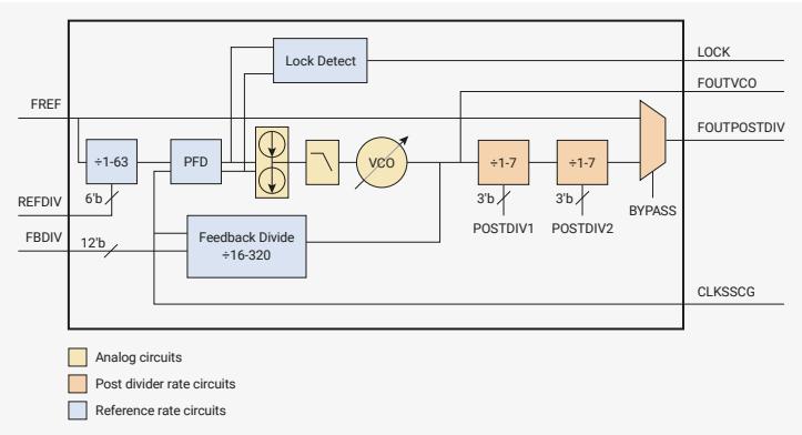
8.6.3. Calculating PLL parameters
To configure the PLL, you must know the frequency of the reference clock, which is routed directly from the crystal oscillator. This will often be a 12 MHz crystal, for compatibility with RP2350's USB bootrom. The PLL's final output frequency \( F_{OUTPOSTDIV} \) can then be calculated as \( (F_{REF} / REF_{DIV}) \times F_{BDIV} / (POSTDIV1 \times POSTDIV2) \) . With a desired output frequency in mind, you must select PLL parameters according to the following constraints of the PLL design:
- • minimum reference frequency ( \( F_{REF} / REF_{DIV} \) ) is 5 MHz
- • oscillator frequency ( \( F_{OUTVCO} \) ) must be in the range 750 MHz-1600 MHz
- • feedback divider ( \( F_{BDIV} \) ) must be in the range 16-320
- • the post dividers \( POSTDIV1 \) and \( POSTDIV2 \) must be in the range 1-7
- • maximum input frequency ( \( F_{REF} / REF_{DIV} \) ) is VCO frequency divided by 16, due to minimum feedback divisor
You must also respect the maximum frequencies of the chip's clock generators (attached to \( F_{OUTPOSTDIV} \) ). For the system PLL this is 150 MHz, and for the USB PLL, 48 MHz. If using a crystal oscillator with a frequency of less than 75 MHz, \( REF_{DIV} \) should be 1 assuming a VCO of 1200 MHz-1600 MHz. If using a fast crystal with a low VCO frequency, the reference divisor may need to be increased to keep the PLL input within a suitable range.
 TIP
TIP
When two different values are required for \( POSTDIV1 \) and \( POSTDIV2 \) , assign the higher value to \( POSTDIV1 \) for lower power consumption.
In the RP2350 reference design (see Hardware design with RP2350, Minimal Design Example ), which attaches a 12 MHz crystal to the crystal oscillator, the minimum VCO frequency is \( 12 \text{ MHz} \times 63 = 756 \text{ MHz} \) , and the maximum VCO frequency is \( 12 \text{ MHz} \times 133 = 1596 \text{ MHz} \) . As a result, \( F_{BDIV} \) must remain in the range 63 to 133 to avoid leaving the supported range of VCO frequencies. Setting \( F_{BDIV} \) to 100 would synthesise a 1200 MHz VCO frequency. A \( POSTDIV1 \) value of 6 and a \( POSTDIV2 \) value of 2 would divide this by 12 in total, producing a clean 100 MHz at the PLL's final output.
8.6.3.1. Jitter versus power consumption
Often, several sets of PLL configuration parameters achieve the desired output frequency (or a close approximation). You decide whether to prioritise lower power consumption or lower jitter : cycle-to-cycle variation in the PLL's output clock period. Jitter decreases as VCO frequency increases, because you can use higher post-divide values. Consider the following scenarios:
- • \( 1500 \text{ MHz VCO} / 6 / 2 = 125 \text{ MHz} \)
- • \( 750 \text{ MHz VCO} / 6 / 1 = 125 \text{ MHz} \)
The 1500 MHz configuration uses the most power, but produces the least jitter. The 750 MHz configuration uses the least power, but produces the most jitter.
You can slightly adjust the desired output frequency to allow for a much lower VCO frequency by bringing the output to a closer rational multiple of the input. Some frequencies are not achievable at all with a possible VCO frequency and combination of divisors.
Because RP2350's digital logic compensates for the worst possible jitter on the system clock, this doesn't affect system stability. However, applications often require a highly accurate clock for data transfers that follow the USB specification, which defines a maximum amount of allowable jitter.
8.6.3.2. Calculating parameters with vcocalc.py
SDK provides a Python script that searches for the best VCO and post divider options for a desired output frequency:
SDK: https://github.com/raspberrypi/pico-sdk/blob/master/src/rp2_common/hardware_clocks/scripts/vccalc.py
1  #!/usr/bin/env python3
2
3  import argparse
4  import sys
5
6  # Fixed hardware parameters
7  fbdiv_range = range(16, 320 + 1)
8  postdiv_range = range(1, 7 + 1)
9  ref_min = 5
10 refdiv_min = 1
11 refdiv_max = 63
12
13 def validRefdiv(string):
14     if ((int(string) < refdiv_min) or (int(string) > refdiv_max)):
15         raise ValueError("REFDIV must be in the range {} to {}".format(refdiv_min,
16                                 refdiv_max))
17     return int(string)
18
19 parser = argparse.ArgumentParser(description="PLL parameter calculator")
20 parser.add_argument("--input", "-i", default=12, help="Input (reference) frequency. Default 12 MHz", type=float)
21 parser.add_argument("--ref-min", default=5, help="Override minimum reference frequency. Default 5 MHz", type=float)
22 parser.add_argument("--vco-max", default=1600, help="Override maximum VCO frequency. Default 1600 MHz", type=float)
23 parser.add_argument("--vco-min", default=750, help="Override minimum VCO frequency. Default 750 MHz", type=float)
24 parser.add_argument("--cmake", action="store_true", help="Print out a CMake snippet to apply the selected PLL parameters to your program")
25 parser.add_argument("--cmake-only", action="store_true", help="Same as --cmake, but do not print anything other than the CMake output")
26 parser.add_argument("--cmake-executable-name", default="<program>", help="Set the executable name to use in the generated CMake output")
27 parser.add_argument("--lock-refdiv", help="Lock REFDIV to specified number in the range {} to {}".format(refdiv_min, refdiv_max), type=validRefdiv)
28 parser.add_argument("--low-vco", "-l", action="store_true", help="Use a lower VCO frequency when possible. This reduces power consumption, at the cost of increased jitter")
29 args = parser.parse_args()
30
31 refdiv_range = range(refdiv_min, max(refdiv_min, min(refdiv_max, int(args.input / args.ref_min))) + 1)
32 if args.lock_refdiv:
33     print("Locking REFDIV to", args.lock_refdiv)
34     refdiv_range = [args.lock_refdiv]
35
36 best = (0, 0, 0, 0, 0, 0)
37 best_margin = args.output
38
39 for refdiv in refdiv_range:
40     for fbdiv in fbdiv_range:
41         vco = args.input / refdiv * fbdiv
42         if vco < args.vco_min or vco > args.vco_max:
43             continue
44         # pd1 is inner loop so that we prefer higher ratios of pd1:pd2
45         for pd2 in postdiv_range:
46             for pd1 in postdiv_range:
47                 out = vco / pd1 / pd2
48                 margin = abs(out - args.output)
49                 vco_is_better = vco < best[5] if args.low_vco else vco > best[5]
50                 if ((vco * 1000) % (pd1 * pd2)):
51         continue
52         if margin < best_margin or (abs(margin - best_margin) < 1e-9 and
vco_is_better):
53             best = (out, fbdiv, pd1, pd2, refdiv, vco)
54             best_margin = margin
55
56 best_out, best_fbdiv, best_pd1, best_pd2, best_refdiv, best_vco = best
57
58 if best[0] > 0:
59     cmake_output = \
60 f"""target_compile_definitions({args.cmake_executable_name} PRIVATE
61     PLL_SYS_REFDIV={best_refdiv}
62     PLL_SYS_VCO_FREQ_HZ={int((args.input * 1_000_000) / best_refdiv * best_fbdiv)}
63     PLL_SYS_POSTDIV1={best_pd1}
64     PLL_SYS_POSTDIV2={best_pd2}
65     SYS_CLK_HZ={int((args.input * 1_000_000) / (best_refdiv * best_pd1 * best_pd2) *
best_fbdiv)}
66 )
67 """
68     if not args.cmake_only:
69         print("Requested: {} MHz".format(args.output))
70         print("Achieved: {} MHz".format(best_out))
71         print("REFDIV: {}".format(best_refdiv))
72         print("FBDIV: {} (VCO = {} MHz)".format(best_fbdiv, args.input / best_refdiv *
best_fbdiv))
73         print("PD1: {}".format(best_pd1))
74         print("PD2: {}".format(best_pd2))
75         if best_refdiv != 1:
76             print(
77                 "\nThis requires a non-default REFDIV value.\n"
78                 "Add the following to your CMakeLists.txt to apply the REFDIV:\n"
79             )
80         elif args.cmake or args.cmake_only:
81             print("")
82         if args.cmake or args.cmake_only or best_refdiv != 1:
83             print(cmake_output)
84     else:
85         sys.exit("No solution found")
Given an input and output frequency, this script finds the best possible set of PLL parameters. When the script finds multiple equally good combinations, it returns the parameters which yield the highest VCO frequency, for the best output stability. Pass the
-l
or
--low-vco
flag to prefer lower frequencies, which reduce power consumption. Pass the
--vco-max
flag to limit the maximum VCO frequency. If the script cannot find an exact match given the provided constraints, it outputs the closest reasonable match instead.
The following example uses the script to request a 48 MHz output with the best output stability:
$ ./vcocalc.py 48
Requested: 48.0 MHz
Achieved: 48.0 MHz
REFDIV: 1
FBDIV: 120 (VCO = 1440.0 MHz)
PD1: 6
PD2: 5
This can also be output as CMake for configuring an SDK application:
$ ./vcocalc.py 48 --cmake
Requested: 48.0 MHz
Achieved: 48.0 MHz
REFDIV: 1
FBDIV: 120 (VCO = 1440.0 MHz)
PD1: 6
PD2: 5

target_compile_definitions(<program> PRIVATE
    PLL_SYS_REFDIV=1
    PLL_SYS_VCO_FREQ_HZ=1440000000
    PLL_SYS_POSTDIV1=6
    PLL_SYS_POSTDIV2=5
)
You can also pass
--cmake-only
to get just the CMake output, and
--cmake-executable-name
to replace the
<program>
with the name of the target program you are configuring.
The following example uses the script to request a 48 MHz output with the lowest power consumption:
$ ./vcocalc.py -l 48
Requested: 48.0 MHz
Achieved: 48.0 MHz
REFDIV: 1
FBDIV: 64 (VCO = 768.0 MHz)
PD1: 4
PD2: 4
The following example uses the script to request a 125 MHz output with the lowest power consumption, with the reference divisor REFDIV fixed at a value of 1. Even though we stated a preference for slower VCO frequencies, the resulting frequency remains quite high:
$ ./vcocalc.py -l 125 --lock-refdiv=1
Requested: 125.0 MHz
Achieved: 125.0 MHz
REFDIV: 1
FBDIV: 125 (VCO = 1500.0 MHz)
PD1: 6
PD2: 2
This happens when the best match for your requested output requires a high VCO frequency. The script always returns the best match, preferring lower VCO frequencies only when there are multiple, equally good matches.
You can work around this by restricting the upper VCO frequency. The following example uses the script to request a 125 MHz system clock, restricting the search to VCO frequencies below 800 MHz. There is no exact match, so the script considers near (but not exact) frequency matches. Relaxing the search to allow nearby non-exact matches significantly reduces the minimum VCO frequency compared to the previous example:
$ ./vcocalc.py -l 125 --lock-refdiv=1 --vco-max=800
Locking REFDIV to 1
Requested: 125.0 MHz
Achieved: 126.0 MHz
REFDIV: 1
FBDIV: 63 (VCO = 756.0 MHz)
PD1: 6
PD2: 1
A 126 MHz system clock may be a tolerable deviation from the desired 125 MHz, and generating this clock consumes less power at the PLL.
By default the script also searches reference divisors, which may give a closer match to your requested output, or enable higher or lower VCO frequencies (depending on preference). The following example allows the script to search FBDIV values:
$ ./vcocalc.py -l 125
Requested: 125.0 MHz
Achieved: 125.0 MHz
REFDIV:   2
FBDIV:    125 (VCO = 750.0 MHz)
PD1:      6
PD2:      1

This requires a non-default REFDIV value.
Add the following to your CMakeLists.txt to apply the REFDIV:

target_compile_definitions(<program> PRIVATE
    PLL_SYS_REFDIV=2
    PLL_SYS_VCO_FREQ_HZ=750000000
    PLL_SYS_POSTDIV1=6
    PLL_SYS_POSTDIV2=1
)
This finds a solution with exactly the requested output, at exactly the minimum VCO frequency of 750 MHz.
All of the above assume a 12 MHz crystal. RP2350 supports a range of XOSC frequencies documented in Section 8.2, “Crystal oscillator (XOSC)” . Suppose we had a 32 MHz crystal, and required a 150 MHz system clock, the maximum supported on RP2350. You can specify the input frequency with the --input or -i flag, as shown in the following example:
$. /vcocalc.py 150 -i 32
Requested: 150.0 MHz
Achieved: 150.0 MHz
REFDIV:   2
FBDIV:    75 (VCO = 1200.0 MHz)
PD1:      4
PD2:      2

This requires a non-default REFDIV value.
Add the following to your CMakeLists.txt to apply the REFDIV:

target_compile_definitions(<program> PRIVATE
    PLL_SYS_REFDIV=2
    PLL_SYS_VCO_FREQ_HZ=1200000000
    PLL_SYS_POSTDIV1=4
    PLL_SYS_POSTDIV2=2
)
8.6.4. Configuration
The SDK uses the following PLL settings:
SDK: https://github.com/raspberrypi/pico-sdk/blob/master/src/rp2-common/hardware_clocks/include/hardware/clocks.h Lines 143 - 164
143 // There are two PLLs in RP-series microcontrollers:
144 // 1. The 'SYS PLL' generates the system clock, the frequency is defined by `SYS_CLK_KHZ`.
145 // 2. The 'USB PLL' generates the USB clock, the frequency is defined by `USB_CLK_KHZ`.
146 //
147 // The two PLLs use the crystal oscillator output directly as their reference frequency input;
    the PLLs reference
148 // frequency cannot be reduced by the dividers present in the clocks block. The crystal
    frequency is defined by `XOSC_HZ` (or
149 // `XOSC_KHZ` or `XOSC_MHZ`).
150 //
151 // The system's default definitions are correct for the above frequencies with a 12MHz
152 // crystal frequency. If different frequencies are required, these must be defined in
153 // the board configuration file together with the revised PLL settings
154 // Use `vcocalc.py` to check and calculate new PLL settings if you change any of these
    frequencies.
155 //
156 // Default PLL configuration RP2040:
157 //          REF      FBDIV VCO          POSTDIV
158 // PLL SYS: 12 / 1 = 12MHz * 125 = 1500MHz / 6 / 2 = 125MHz
159 // PLL USB: 12 / 1 = 12MHz * 100 = 1200MHz / 5 / 5 = 48MHz
160 //
161 // Default PLL configuration RP2350:
162 //          REF      FBDIV VCO          POSTDIV
163 // PLL SYS: 12 / 1 = 12MHz * 125 = 1500MHz / 5 / 2 = 150MHz
164 // PLL USB: 12 / 1 = 12MHz * 100 = 1200MHz / 5 / 5 = 48MHz
The
pll_init
function in the SDK (examined below) asserts that all of these conditions are true before attempting to configure the PLL.
The SDK defines the PLL control registers as a struct. It then maps them into memory for each instance of the PLL.
SDK: https://github.com/raspberrypi/pico-sdk/blob/master/src/rp2350/hardware_structs/include/hardware/structs/pll.h Lines 27 - 74
27 typedef struct {
28     _REG_(PLL_CS_OFFSET) // PLL_CS
29     // Control and Status
30     // 0x80000000 [31] LOCK          (0) PLL is locked
31     // 0x40000000 [30] LOCK_N       (0) PLL is not locked +
32     // 0x00000100 [8]  BYPASS       (0) Passes the reference clock to the output instead of
    the...
33     // 0x0000003f [5:0] REFDIV      (0x01) Divides the PLL input reference clock
34     io_rw_32 cs;
35
36     _REG_(PLL_PWR_OFFSET) // PLL_PWR
37     // Controls the PLL power modes
38     // 0x00000020 [5]  VCOPD        (1) PLL VCO powerdown +
39     // 0x00000008 [3]  POSTDIVPD    (1) PLL post divider powerdown +
40     // 0x00000004 [2]  DSMPD        (1) PLL DSM powerdown +
41     // 0x00000001 [0]  PD           (1) PLL powerdown +
42     io_rw_32 pwr;
43
44     _REG_(PLL_FBDIV_INT_OFFSET) // PLL_FBDIV_INT
45     // Feedback divisor
46     // 0x00000fff [11:0] FBDIV_INT  (0x000) see ctrl reg description for constraints
47     io_rw_32 fbdiv_int;
48
49     _REG_(PLL_PRIM_OFFSET) // PLL_PRIM
50     // Controls the PLL post dividers for the primary output
51     // 0x00070000 [18:16] POSTDIV1   (0x7) divide by 1-7
52     // 0x00070000 [14:12] POSTDIV2   (0x7) divide by 1-7
53     io_rw_32 prim;
54
55     _REG_(PLL_INTR_OFFSET) // PLL_INTR
56     // Raw Interrupts
57     // 0x00000001 [0]     LOCK_N_STICKY (0)
58     io_rw_32 intr;
59
60     _REG_(PLL_INTE_OFFSET) // PLL_INTE
61     // Interrupt Enable
62     // 0x00000001 [0]     LOCK_N_STICKY (0)
63     io_rw_32 inte;
64
65     _REG_(PLL_INTF_OFFSET) // PLL_INTF
66     // Interrupt Force
67     // 0x00000001 [0]     LOCK_N_STICKY (0)
68     io_rw_32 intf;
69
70     _REG_(PLL_INTS_OFFSET) // PLL_INTS
71     // Interrupt status after masking & forcing
72     // 0x00000001 [0]     LOCK_N_STICKY (0)
73     io_ro_32 ints;
74 } pll_hw_t;
The SDK defines
pll_init
, which is used to configure or reconfigure a PLL. It starts by clearing any previous power state in the PLL, then calculates the appropriate feedback divider value. There are assertions to check that these values satisfy the constraints above.
SDK: https://github.com/raspberrypi/pico-sdk/blob/master/src/rp2_common/hardware_pll/pll.c Lines 13 - 21
13 void pll_init(PLL pll, uint refdiv, uint vco_freq, uint post_div1, uint post_div2) {
14     uint32_t ref_freq = XOSC_HZ / refdiv;
15
16     // Check vco freq is in an acceptable range
17     assert(vco_freq >= PICO_PLL_VCO_MIN_FREQ_HZ && vco_freq <= PICO_PLL_VCO_MAX_FREQ_HZ);
18
19     // What are we multiplying the reference clock by to get the vco freq
20     // (The regs are called div, because you divide the vco output and compare it to the
21     // refclk)
22     uint32_t fbdiv = vco_freq / ref_freq;
The programming sequence for the PLL is as follows:
- 1. Program the reference clock divider (is a divide by 1 in the RP2350 case).
- 2. Program the feedback divider.
- 3. Turn on the main power and VCO.
- 4. Wait for the VCO to achieve a stable frequency, as indicated by the
LOCKstatus flag. - 5. Set up post dividers and turn them on.
SDK: https://github.com/raspberrypi/pico-sdk/blob/master/src/rp2_common/hardware_pll/pll.c Lines 42 - 69
42     if ((pll->cs & PLL_CS_LOCK_BITS) &&
43         (refdiv == (pll->cs & PLL_CS_REFDIV_BITS)) &&
44         (fbdiv == (pll->fbdiv_int & PLL_FBDIV_INT_BITS)) &&
45         (pdv == (pll->prim & (PLL_PRIM_POSTDIV1_BITS | PLL_PRIM_POSTDIV2_BITS)))) {
46         // do not disrupt PLL that is already correctly configured and operating
47         return;
48     }
49
50     reset_unreset_block_num_wait_blocking(PLL_RESET_NUM(p11));
51
52     // Load VCO-related dividers before starting VCO
53     pll->cs = refdiv;
54     pll->fbdiv_int = fbdiv;
55
56     // Turn on PLL
57     uint32_t power = PLL_PWR_PD_BITS | // Main power
58                   PLL_PWR_VCPD_BITS; // VCO Power
59
60     hw_clear_bits(&pll->pwr, power);
61
62     // Wait for PLL to lock
63     while (!(pll->cs & PLL_CS_LOCK_BITS)) tight_loop_contents();
64
65     // Set up post dividers
66     pll->prim = pdiv;
67
68     // Turn on post divider
69     hw_clear_bits(&pll->pwr, PLL_PWR_POSTDIVPD_BITS);
The VCO turns on first, followed by the post dividers, so the PLL does not output a dirty clock while waiting for the VCO to lock.
8.6.5. List of Registers
The PLL_SYS and PLL_USB registers start at base addresses of 0x40050000 and 0x40058000 respectively (defined as PLL_SYS_BASE and PLL_USB_BASE in SDK).
Table 636. List of PLL registers
| Offset | Name | Info |
|---|---|---|
| 0x00 | CS | Control and Status |
| 0x04 | PWR | Controls the PLL power modes. |
| 0x08 | FBDIV_INT | Feedback divisor |
| 0x0c | PRIM | Controls the PLL post dividers for the primary output |
| 0x10 | INTR | Raw Interrupts |
| 0x14 | INTE | Interrupt Enable |
| 0x18 | INTF | Interrupt Force |
| 0x1c | INTS | Interrupt status after masking & forcing |
PLL: CS Register
Offset: 0x00
Description
Control and Status
GENERAL CONSTRAINTS:
Reference clock frequency min=5MHz, max=800MHz
Feedback divider min=16, max=320
VCO frequency min=400MHz, max=1600MHz
Table 637. CS Register
| Bits | Description | Type | Reset |
|---|---|---|---|
| 31 | LOCK: PLL is locked | RO | 0x0 |
| Bits | Description | Type | Reset |
|---|---|---|---|
| 30 | LOCK_N
: PLL is not locked Ideally this is cleared when PLL lock is seen and this should never normally be set | WC | 0x0 |
| 29:9 | Reserved. | - | - |
| 8 | BYPASS : Passes the reference clock to the output instead of the divided VCO. The VCO continues to run so the user can switch between the reference clock and the divided VCO but the output will glitch when doing so. | RW | 0x0 |
| 7:6 | Reserved. | - | - |
| 5:0 | REFDIV
: Divides the PLL input reference clock. Behaviour is undefined for div=0. PLL output will be unpredictable during reldiv changes, wait for lock=1 before using it. | RW | 0x01 |
PLL: PWR Register
Offset: 0x04
Description
Controls the PLL power modes.
Table 638. PWR Register
| Bits | Description | Type | Reset |
|---|---|---|---|
| 31:6 | Reserved. | - | - |
| 5 | VCOPD
: PLL VCO powerdown To save power set high when PLL output not required or bypass=1. | RW | 0x1 |
| 4 | Reserved. | - | - |
| 3 | POSTDIVPD
: PLL post divider powerdown To save power set high when PLL output not required or bypass=1. | RW | 0x1 |
| 2 | DSMPD
: PLL DSM powerdown Nothing is achieved by setting this low. | RW | 0x1 |
| 1 | Reserved. | - | - |
| 0 | PD
: PLL powerdown To save power set high when PLL output not required. | RW | 0x1 |
PLL: FBDIV_INT Register
Offset: 0x08
Description
Feedback divisor
(note: this PLL does not support fractional division)
Table 639. FBDIV_INT Register
| Bits | Description | Type | Reset |
|---|---|---|---|
| 31:12 | Reserved. | - | - |
| 11:0 | see ctrl reg description for constraints | RW | 0x000 |
PLL: PRIM Register
Offset: 0x0c
DescriptionControls the PLL post dividers for the primary output
(note: this PLL does not have a secondary output)
the primary output is driven from VCO divided by
\(
\text{postdiv1} * \text{postdiv2}
\)
Table 640. PRIM
Register
| Bits | Description | Type | Reset |
|---|---|---|---|
| 31:19 | Reserved. | - | - |
| 18:16 | POSTDIV1 : divide by 1-7 | RW | 0x7 |
| 15 | Reserved. | - | - |
| 14:12 | POSTDIV2 : divide by 1-7 | RW | 0x7 |
| 11:0 | Reserved. | - | - |
Offset: 0x10
DescriptionRaw Interrupts
Table 641. INTR
Register
| Bits | Description | Type | Reset |
|---|---|---|---|
| 31:1 | Reserved. | - | - |
| 0 | LOCK_N_STICKY | WC | 0x0 |
Offset: 0x14
DescriptionInterrupt Enable
Table 642. INTE
Register
| Bits | Description | Type | Reset |
|---|---|---|---|
| 31:1 | Reserved. | - | - |
| 0 | LOCK_N_STICKY | RW | 0x0 |
Offset: 0x18
DescriptionInterrupt Force
Table 643. INTF
Register
| Bits | Description | Type | Reset |
|---|---|---|---|
| 31:1 | Reserved. | - | - |
| 0 | LOCK_N_STICKY | RW | 0x0 |
Offset: 0x1c
DescriptionInterrupt status after masking & forcing
Table 644. INTS
Register
| Bits | Description | Type | Reset |
|---|---|---|---|
| 31:1 | Reserved. | - | - |
| 0 | LOCK_N_STICKY | RO | 0x0 |