9. GPIO
 CAUTION
Under certain conditions, pull-down does not function as expected. For more information, see RP2350-E9 .
9.1. Overview
RP2350 has up to 54 multi-functional General Purpose Input / Output (GPIO) pins, divided into two banks:
Bank 0
30 user GPIOs in the QFN-60 package (RP2350A), or 48 user GPIOs in the QFN-80 package
Bank 1
six QSPI IOs, and the USB DP/DM pins
You can control each GPIO from software running on the processors, or by a number of other functional blocks. To meet USB rise and fall specifications, the analogue characteristics of the USB pins differ from the GPIO pads. As a result, we do not include them in the 54 GPIO total. However, you can still use them for UART, I2C, or processor-controlled GPIO through the single-cycle IO subsystem (SIO).
In a typical use case, the QSPI IOs are used to execute code from an external flash device, leaving 30 or 48 Bank 0 GPIOs for the programmer to use. The QSPI pins might become available for general purpose use when booting the chip from internal OTP, or controlling the chip externally through SWD in an IO expander application.
All GPIOs support digital input and output. Several Bank 0 GPIOs can also be used as inputs to the chip's Analogue to Digital Converter (ADC):
- • GPIOs 26 through 29 inclusive (four total) in the QFN-60 package
- • GPIOs 40 through 47 (eight total) in the QFN-80 package
Bank 0 supports the following functions:
- • Software control via SIO — Section 3.1.3, “GPIO control”
- • Programmable IO (PIO) — Chapter 11, PIO
- • 2 × SPI — Section 12.3, “SPI”
- • 2 × UART — Section 12.1, “UART”
- • 2 × I2C (two-wire serial interface) — Section 12.2, “I2C”
- • 8 × two-channel PWM in the QFN-60 package, or 12 × in QFN-80 — Section 12.5, “PWM”
- • 2 × external clock inputs — Section 8.1.2.4, “External clocks”
- • 4 × general purpose clock output — Section 8.1, “Overview”
- • 4 × input to ADC in the QFN-60 package, or 8 × in QFN-80 — Section 12.4, “ADC and Temperature Sensor”
- • 1 × HSTX high-speed interface — Section 12.11, “HSTX”
- • 1 × auxiliary QSPI chip select, for a second XIP device — Section 12.14, “QSPI memory interface (QMI)”
- • CoreSight execution trace output — Section 3.5.7, “Trace”
- • USB VBUS management — Section 12.7.3.10, “VBUS control”
- • External interrupt requests, level or edge-sensitive — Section 9.5, “Interrupts”
Bank 1 contains the QSPI and USB DP/DM pins and supports the following functions:
- • Software control via SIO — Section 3.1.3, “GPIO control”
- • Flash execute in place ( Section 4.4, “External flash and PSRAM (XIP)” ) via QSPI Memory Interface (QMI) — Section 12.14, “QSPI memory interface (QMI)”
- • UART — Section 12.1, “UART”
- • I2C (two-wire serial interface) — Section 12.2, “I2C”
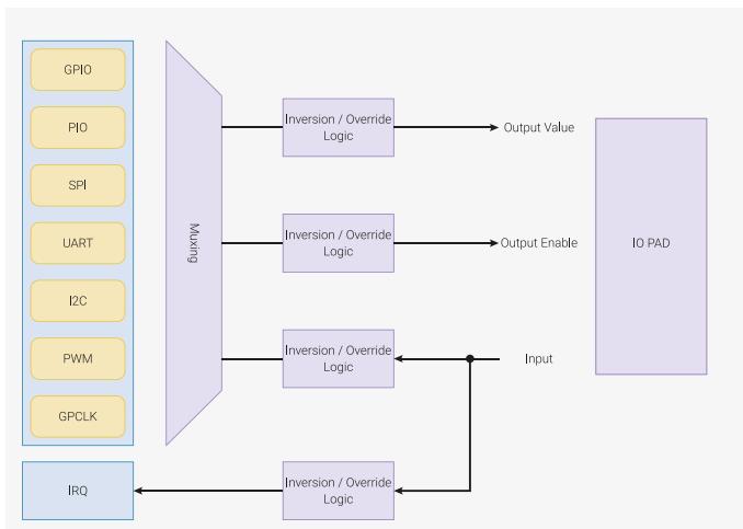
The logical structure of an example IO is shown in Figure 41 .
Figure 41. Logical structure of a GPIO. Each GPIO can be controlled by one of a number of peripherals, or by software control registers in the SIO. The function select (FSEL) selects which peripheral output is in control of the GPIO's direction and output level, and which peripheral input can see this GPIO's input level. These three signals (output level, output enable, input level) can also be inverted or forced high or low, using the GPIO control registers.
9.2. Changes from RP2040
RP2350 GPIO differs from RP2040 in the following ways:
- • 18 more GPIOs in the QFN-80 package
- • Addition of a third PIO to GPIO functions
- • USB DP/DM pins can be used as GPIO
- • Addition of isolation register to pad registers (preserves pad state while in a low power state, cleared by software on power up)
- • Changed default reset state of pad controls
- • Both Secure and Non-secure access to GPIOs (see Section 10.6 )
- • Double the number of GPIO interrupts to differentiate between Secure and Non-secure
- • Interrupt summary registers added so you can quickly see which GPIOs have pending interrupts
9.3. Reset state
At first power up, Bank 0 IOs (GPIOs 0 through 29 in the QFN-60 package, and GPIOs 0 through 47 in the QFN-80 package) assume the following state:
- • Output buffer is high-impedance
- • Input buffer is disabled
- • Pulled low
- • Isolation latches are set to latched ( Section 9.7 )
The pad output disable bit ( GPIO0.OD ) for each pad is clear at reset, but the IO muxing is reset to the null function,
which ensures that the output buffer is high-impedance.
! IMPORTANT
The pad reset state is different from RP2040, which only disables digital inputs on GPIOs 26 through 29 (as of version B2) and does not have isolation latches. Applications must enable the pad input (
GPIO0.IE = 1
) and disable pad isolation latches (
GPIO0.ISO = 0
) before using the pads for digital I/O. The
gpio_set_function()
SDK function performs these tasks automatically.
Bank 1 IOs have the same reset state as Bank 0 GPIOs, except for the input enable (IE) resetting to 1, and different pull-up/pull-down states: SCK, SD0 and SD1 are pull-down, but SD2, SD3 and CSn are pull-up.
i NOTE
To use a Bank 0 GPIO as a second chip select, you need an external pull-up to ensure the second QSPI device does not power up with its chip select asserted.
The pads return to the reset state on any of the following:
- • A brownout reset
- • Asserting the RUN pin low
- • Setting SW-DP CDBGSTREQ via SWD
- • Setting RP-AP rescue reset via SWD
If a pad's isolation latches are in the latched state ( Section 9.7 ) then resetting the PADS and IO registers does not physically return the pad to its reset state. The isolation latches prevent upstream signals from propagating to the pad. Clear the ISO bit to allow signals to propagate.
9.4. Function select
To allocate a function to a GPIO, write to the
FUNCSEL
field in the
CTRL
register corresponding to the pin. For a list of GPIOs and corresponding registers, see
Table 645
. For an example, see
GPIO0_CTRL
. The descriptions for the functions listed in this table can be found in
Table 646
.
Each GPIO can only select one function at a time. Each peripheral input (e.g. UART0 RX) should only be selected by one GPIO at a time. If you connect the same peripheral input to multiple GPIOs, the peripheral sees the logical OR of these GPIO inputs.
Table 645. General Purpose Input/Output (GPIO) Bank 0 Functions
| GPIO | F0 | F1 | F2 | F3 | F4 | F5 | F6 | F7 | F8 | F9 | F10 | F11 |
|---|---|---|---|---|---|---|---|---|---|---|---|---|
| 0 | SPI0 RX | UART0 TX | I2C0 SDA | PWM0 A | SIO | PI00 | PI01 | PI02 | QMI CS1n | USB OVCUR DET | ||
| 1 | SPI0 CSn | UART0 RX | I2C0 SCL | PWM0 B | SIO | PI00 | PI01 | PI02 | TRACECLK | USB VBUS DET | ||
| 2 | SPI0 SCK | UART0 CTS | I2C1 SDA | PWM1 A | SIO | PI00 | PI01 | PI02 | TRACEDATA0 | USB VBUS EN | UART0 TX | |
| 3 | SPI0 TX | UART0 RTS | I2C1 SCL | PWM1 B | SIO | PI00 | PI01 | PI02 | TRACEDATA1 | USB OVCUR DET | UART0 RX | |
| 4 | SPI0 RX | UART1 TX | I2C0 SDA | PWM2 A | SIO | PI00 | PI01 | PI02 | TRACEDATA2 | USB VBUS DET | ||
| 5 | SPI0 CSn | UART1 RX | I2C0 SCL | PWM2 B | SIO | PI00 | PI01 | PI02 | TRACEDATA3 | USB VBUS EN | ||
| 6 | SPI0 SCK | UART1 CTS | I2C1 SDA | PWM3 A | SIO | PI00 | PI01 | PI02 | USB OVCUR DET | UART1 TX | ||
| 7 | SPI0 TX | UART1 RTS | I2C1 SCL | PWM3 B | SIO | PI00 | PI01 | PI02 | USB VBUS DET | UART1 RX | ||
| 8 | SPI1 RX | UART1 TX | I2C0 SDA | PWM4 A | SIO | PI00 | PI01 | PI02 | QMI CS1n | USB VBUS EN | ||
| 9 | SPI1 CSn | UART1 RX | I2C0 SCL | PWM4 B | SIO | PI00 | PI01 | PI02 | USB OVCUR DET | |||
| 10 | SPI1 SCK | UART1 CTS | I2C1 SDA | PWM5 A | SIO | PI00 | PI01 | PI02 | USB VBUS DET | UART1 TX | ||
| 11 | SPI1 TX | UART1 RTS | I2C1 SCL | PWM5 B | SIO | PI00 | PI01 | PI02 | USB VBUS EN | UART1 RX | ||
| 12 | HSTX | SPI1 RX | UART0 TX | I2C0 SDA | PWM6 A | SIO | PI00 | PI01 | PI02 | CLOCK GPIN0 | USB OVCUR DET | |
| 13 | HSTX | SPI1 CSn | UART0 RX | I2C0 SCL | PWM6 B | SIO | PI00 | PI01 | PI02 | CLOCK GPOUT0 | USB VBUS DET | |
| 14 | HSTX | SPI1 SCK | UART0 CTS | I2C1 SDA | PWM7 A | SIO | PI00 | PI01 | PI02 | CLOCK GPIN1 | USB VBUS EN | UART0 TX |
| 15 | HSTX | SPI1 TX | UART0 RTS | I2C1 SCL | PWM7 B | SIO | PI00 | PI01 | PI02 | CLOCK GPOUT1 | USB OVCUR DET | UART0 RX |
| 16 | HSTX | SPI0 RX | UART0 TX | I2C0 SDA | PWM0 A | SIO | PI00 | PI01 | PI02 | USB VBUS DET | ||
| 17 | HSTX | SPI0 CSn | UART0 RX | I2C0 SCL | PWM0 B | SIO | PI00 | PI01 | PI02 | USB VBUS EN | ||
| 18 | HSTX | SPI0 SCK | UART0 CTS | I2C1 SDA | PWM1 A | SIO | PI00 | PI01 | PI02 | USB OVCUR DET | UART0 TX | |
| 19 | HSTX | SPI0 TX | UART0 RTS | I2C1 SCL | PWM1 B | SIO | PI00 | PI01 | PI02 | QMI CS1n | USB VBUS DET | UART0 RX |
| 20 | SPI0 RX | UART1 TX | I2C0 SDA | PWM2 A | SIO | PI00 | PI01 | PI02 | CLOCK GPIN0 | USB VBUS EN | ||
| 21 | SPI0 CSn | UART1 RX | I2C0 SCL | PWM2 B | SIO | PI00 | PI01 | PI02 | CLOCK GPOUT0 | USB OVCUR DET | ||
| 22 | SPI0 SCK | UART1 CTS | I2C1 SDA | PWM3 A | SIO | PI00 | PI01 | PI02 | CLOCK GPIN1 | USB VBUS DET | UART1 TX |
| GPIO | F0 | F1 | F2 | F3 | F4 | F5 | F6 | F7 | F8 | F9 | F10 | F11 |
|---|---|---|---|---|---|---|---|---|---|---|---|---|
| 23 | SPI0 TX | UART1 RTS | I2C1 SCL | PWM3 B | SIO | PI00 | PI01 | PI02 | CLOCK GPOUT1 | USB VBUS EN | UART1 RX | |
| 24 | SPI1 RX | UART1 TX | I2C0 SDA | PWM4 A | SIO | PI00 | PI01 | PI02 | CLOCK GPOUT2 | USB OVCCR DET | ||
| 25 | SPI1 CSn | UART1 RX | I2C0 SCL | PWM4 B | SIO | PI00 | PI01 | PI02 | CLOCK GPOUT3 | USB VBUS DET | ||
| 26 | SPI1 SCK | UART1 CTS | I2C1 SDA | PWM5 A | SIO | PI00 | PI01 | PI02 | USB VBUS EN | UART1 TX | ||
| 27 | SPI1 TX | UART1 RTS | I2C1 SCL | PWM5 B | SIO | PI00 | PI01 | PI02 | USB OVCCR DET | UART1 RX | ||
| 28 | SPI1 RX | UART0 TX | I2C0 SDA | PWM6 A | SIO | PI00 | PI01 | PI02 | USB VBUS DET | |||
| 29 | SPI1 CSn | UART0 RX | I2C0 SCL | PWM6 B | SIO | PI00 | PI01 | PI02 | USB VBUS EN | |||
| GPIOs 30 through 47 are QFN-80 only: | ||||||||||||
| 30 | SPI1 SCK | UART0 CTS | I2C1 SDA | PWM7 A | SIO | PI00 | PI01 | PI02 | USB OVCCR DET | UART0 TX | ||
| 31 | SPI1 TX | UART0 RTS | I2C1 SCL | PWM7 B | SIO | PI00 | PI01 | PI02 | USB VBUS DET | UART0 RX | ||
| 32 | SPI0 RX | UART0 TX | I2C0 SDA | PWM8 A | SIO | PI00 | PI01 | PI02 | USB VBUS EN | |||
| 33 | SPI0 CSn | UART0 RX | I2C0 SCL | PWM8 B | SIO | PI00 | PI01 | PI02 | USB OVCCR DET | |||
| 34 | SPI0 SCK | UART0 CTS | I2C1 SDA | PWM9 A | SIO | PI00 | PI01 | PI02 | USB VBUS DET | UART0 TX | ||
| 35 | SPI0 TX | UART0 RTS | I2C1 SCL | PWM9 B | SIO | PI00 | PI01 | PI02 | USB VBUS EN | UART0 RX | ||
| 36 | SPI0 RX | UART1 TX | I2C0 SDA | PWM10 A | SIO | PI00 | PI01 | PI02 | USB OVCCR DET | |||
| 37 | SPI0 CSn | UART1 RX | I2C0 SCL | PWM10 B | SIO | PI00 | PI01 | PI02 | USB VBUS DET | |||
| 38 | SPI0 SCK | UART1 CTS | I2C1 SDA | PWM11 A | SIO | PI00 | PI01 | PI02 | USB VBUS EN | UART1 TX | ||
| 39 | SPI0 TX | UART1 RTS | I2C1 SCL | PWM11 B | SIO | PI00 | PI01 | PI02 | USB OVCCR DET | UART1 RX | ||
| 40 | SPI1 RX | UART1 TX | I2C0 SDA | PWM8 A | SIO | PI00 | PI01 | PI02 | USB VBUS DET | |||
| 41 | SPI1 CSn | UART1 RX | I2C0 SCL | PWM8 B | SIO | PI00 | PI01 | PI02 | USB VBUS EN | |||
| 42 | SPI1 SCK | UART1 CTS | I2C1 SDA | PWM9 A | SIO | PI00 | PI01 | PI02 | USB OVCCR DET | UART1 TX | ||
| 43 | SPI1 TX | UART1 RTS | I2C1 SCL | PWM9 B | SIO | PI00 | PI01 | PI02 | USB VBUS DET | UART1 RX | ||
| 44 | SPI1 RX | UART0 TX | I2C0 SDA | PWM10 A | SIO | PI00 | PI01 | PI02 | USB VBUS EN | |||
| GPIO | F0 | F1 | F2 | F3 | F4 | F5 | F6 | F7 | F8 | F9 | F10 | F11 |
|---|---|---|---|---|---|---|---|---|---|---|---|---|
| 45 | SPI1 CSn | UART0 RX | I2C0 SCL | PWM10 B | SIO | PI00 | PI01 | PI02 | USB OVCUR DET | |||
| 46 | SPI1 SCK | UART0 CTS | I2C1 SDA | PWM11 A | SIO | PI00 | PI01 | PI02 | USB VBUS DET | UART0 TX | ||
| 47 | SPI1 TX | UART0 RTS | I2C1 SCL | PWM11 B | SIO | PI00 | PI01 | PI02 | QMI CS1n | USB VBUS EN | UART0 RX |
Table 646. GPIO User Bank function descriptions
| Function Name | Description |
|---|---|
| SPIx | Connect one of the internal PL022 SPI peripherals to GPIO. |
| UARTx | Connect one of the internal PL011 UART peripherals to GPIO. |
| I2Cx | Connect one of the internal DW I2C peripherals to GPIO. |
| PWMx A/B | Connect a PWM slice to GPIO. There are twelve PWM slices, each with two output channels (A/B). The B pin can also be used as an input, for frequency and duty cycle measurement. |
| SIO | Software control of GPIO from the Single-cycle IO (SIO) block. The SIO function (F5) must be selected for the processors to drive a GPIO, but the input is always connected, so software can check the state of GPIOs at any time. |
| PIOx | Connect one of the programmable IO blocks (PIO) to GPIO. PIO can implement a wide variety of interfaces, and has its own internal pin mapping hardware, allowing flexible placement of digital interfaces on Bank 0 GPIOs. The PIO function (F6, F7, F8) must be selected for PIO to drive a GPIO, but the input is always connected, so the PIOs can always see the state of all pins. |
| HSTX | Connect the high-speed transmit peripheral (HSTX) to GPIO. |
| CLOCK GPINx | General purpose clock inputs. Can be routed to a number of internal clock domains on RP2350, e.g. to provide a 1Hz clock for the AON Timer, or can be connected to an internal frequency counter. |
| CLOCK GPOUTx | General purpose clock outputs. Can drive a number of internal clocks (including PLL outputs) onto GPIOs, with optional integer divide. |
| TRACECLK, TRACEDATAx | CoreSight execution trace output from Cortex-M33 processors (Arm-only). |
| USB OVCUR DET/VBUS DET/VBUS EN | USB power control signals to/from the internal USB controller. |
| QMI CS1n | Auxiliary chip select for QSPI bus, to allow execute-in-place from an additional flash or PSRAM device. |
Bank 1 function select operates identically to Bank 0, but its registers are in a different register block, starting with USBPHY_DP_CTRL .
Table 647. GPIO Bank 1 Functions
| Pin | F0 | F1 | F2 | F3 | F4 | F5 | F6 | F7 | F8 | F9 | F10 | F11 |
|---|---|---|---|---|---|---|---|---|---|---|---|---|
| USB DP | UART1 TX | I2C0 SDA | SIO | |||||||||
| USB DM | UART1 RX | I2C0 SCL | SIO | |||||||||
| QSPI SCK | QMI SCK | UART1 CTS | I2C1 SDA | SIO | UART1 TX | |||||||
| QSPI CSn | QMI CS0n | UART1 RTS | I2C1 SCL | SIO | UART1 RX | |||||||
| QSPI SD0 | QMI SD0 | UART0 TX | I2C0 SDA | SIO | ||||||||
| QSPI SD1 | QMI SD1 | UART0 RX | I2C0 SCL | SIO | ||||||||
| QSPI SD2 | QMI SD2 | UART0 CTS | I2C1 SDA | SIO | UART0 TX | |||||||
| QSPI SD3 | QMI SD3 | UART0 RTS | I2C1 SCL | SIO | UART0 RX |
Table 648. GPIO bank 1 function descriptions
| Function Name | Description |
|---|---|
| UARTx | Connect one of the internal PL011 UART peripherals to GPIO. |
| I2Cx | Connect one of the internal DW I2C peripherals to GPIO. |
| Function Name | Description |
|---|---|
| SIO | Software control of GPIO, from the single-cycle IO (SIO) block. The SIO function (F5) must be selected for the processors to drive a GPIO, but the input is always connected, so software can check the state of GPIOs at any time. |
| QMI | QSPI memory interface peripheral, used for execute-in-place from external QSPI flash or PSRAM memory devices. |
The six QSPI Bank GPIO pins are typically used by the XIP peripheral to communicate with an external flash device. However, there are two scenarios where the pins can be used as software-controlled GPIOs:
- • If a SPI or Dual-SPI flash device is used for execute-in-place, then the SD2 and SD3 pins are not used for flash access, and can be used for other GPIO functions on the circuit board.
- • If RP2350 is used in a flashless configuration (USB and OTP boot only), then all six pins can be used for software-controlled GPIO functions.
9.5. Interrupts
An interrupt can be generated for every GPIO pin in four scenarios:
- • Level High: the GPIO pin is a logical 1
- • Level Low: the GPIO pin is a logical 0
- • Edge High: the GPIO has transitioned from a logical 0 to a logical 1
- • Edge Low: the GPIO has transitioned from a logical 1 to a logical 0
The level interrupts are not latched. This means that if the pin is a logical 1 and the level high interrupt is active, it will become inactive as soon as the pin changes to a logical 0. The edge interrupts are stored in the INTR register and can be cleared by writing to the INTR register.
There are enable, status, and force registers for three interrupt destinations: proc 0, proc 1, and dormant_wake. For proc 0 the registers are enable ( PROC0_INTE0 ), status ( PROC0_INTS0 ), and force ( PROC0_INTF0 ). Dormant wake is used to wake the ROSC or XOSC up from dormant mode. See Section 6.5.6.2 for more information on dormant mode.
There is an interrupt output for each combination of IO bank, IRQ destination, and security domain. In total there are twelve such outputs:
- • IO Bank 0 to dormant wake (Secure and Non-secure)
- • IO Bank 0 to proc 0 (Secure and Non-secure)
- • IO Bank 0 to proc 1 (Secure and Non-secure)
- • IO QSPI to dormant wake (Secure and Non-secure)
- • IO QSPI to proc 0 (Secure and Non-secure)
- • IO QSPI to proc 1 (Secure and Non-secure)
Each interrupt output has its own array of enable registers (INTE) that configures which GPIO events cause the interrupt to assert. The interrupt asserts when at least one enabled event occurs, and de-asserts when all enabled events have been acknowledged via the relevant INTR register.
This means the user can watch for several GPIO events at once.
Summary registers can be used to quickly check for pending GPIO interrupts. See IRQSUMMARY_PROC0_NONSECURE0 for an example.
9.6. Pads
⚠ CAUTION
Under certain conditions, pull-down does not function as expected. For more information, see RP2350-E9 .
Each GPIO is connected off-chip via a pad . Pads are the electrical interface between the chip's internal logic and external circuitry. They translate signal voltage levels, support higher currents and offer some protection against electrostatic discharge (ESD) events. You can adjust pad electrical behaviour to meet the requirements of external circuitry in the following ways:
- • Output drive strength can be set to 2mA, 4mA, 8mA or 12mA.
- • Output slew rate can be set to slow or fast.
- • Input hysteresis (Schmitt trigger mode) can be enabled.
- • A pull-up or pull-down can be enabled, to set the output signal level when the output driver is disabled.
- • The input buffer can be disabled, to reduce current consumption when the pad is unused, unconnected or connected to an analogue signal.
An example pad is shown in Figure 42 .
Figure 42. Diagram of a single IO pad.
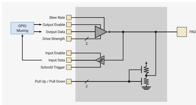
The diagram illustrates the internal structure of a single IO pad. On the left, a 'GPIO Muxing' block is connected to several control signals: Slew Rate, Output Enable, Output Data, Drive Strength, Input Enable, Input Data, Schmitt Trigger, and Pull Up / Pull Down. These signals are routed through a series of multiplexers (indicated by boxes with a '2' and a diagonal line) to the pad's internal logic. The pad's internal logic includes an output driver (a PMOS and NMOS transistor pair) and an input buffer (a PMOS and NMOS transistor pair). The output driver is controlled by the Output Enable, Output Data, and Drive Strength signals. The input buffer is controlled by the Input Enable, Input Data, and Schmitt Trigger signals. The Pull Up / Pull Down signal controls a pull-up or pull-down resistor connected to the pad's input/output node. The pad's input/output node is connected to the external circuitry via a 'PAD' block, represented by a yellow box with a grid pattern.
The pad's Output Enable, Output Data and Input Data ports connect, via the IO mux, to the function controlling the pad. All other ports are controlled from the pad control register. You can use this register to disable the pad's output driver by overriding the Output Enable signal from the function controlling the pad. See GPIO0 for an example of a pad control register.
Both the output signal level and acceptable input signal level at the pad are determined by the digital IO supply (IOVDD). IOVDD can be any nominal voltage between 1.8V and 3.3V, but to meet specification when powered at 1.8V, the pad input thresholds must be adjusted by writing a 1 to the pad VOLTAGE_SELECT registers. By default, the pad input thresholds are valid for an IOVDD voltage between 2.5V and 3.3V. Using a voltage of 1.8V with the default input thresholds is a safe operating mode, but it will result in input thresholds that don't meet specification.
⚠ WARNING
Using IOVDD voltages greater than 1.8V, with the input thresholds set for 1.8V may result in damage to the chip.
Pad input threshold are adjusted on a per bank basis, with separate VOLTAGE_SELECT registers for the pads associated with the User IO bank (IO Bank 0) and the QSPI IO bank. However, both banks share the same digital IO supply (IOVDD), so both register should always be set to the same value.
Pad register details are available in Section 9.11.3, "Pad Control - User Bank" and Section 9.11.4, "Pad Control - QSPI Bank" .
9.6.1. Bus keeper mode
For each pad, only the pull-up or the pull-down resistor can be enabled at any given time. It is impossible to enable both simultaneously. Instead, if you set both the
GPIO0.PDE
and
GPIO0.PUE
bits simultaneously then you enable
bus keeper
mode, where the pad is:
- • Pulled up when its input is high.
- • Pulled down when its input is low.
When the output buffer is disabled, and the pad is not driven by any external source, this mode weakly retains the pad's current logical state. The pad does not float to mid-rail.
Bus keeper mode relies on control logic in the switched core domain, so does not function when the core is powered down. Rather, powering down the core when bus keeper mode is enabled latches the current output controls (pull-up or pull-down) in the pad isolation latches, as described in Section 9.7 .
9.7. Pad isolation latches
RP2350 features extended low-power states that allow all internal logic, with the exception of POWMAN and some CoreSight debug logic, to fully power down under software control. This includes powering down all peripherals, the IO muxing, and the pad control registers, which brings with it the risk that pad signals may experience unwanted transitions when entering and exiting low-power states.
To ensure that pad states are well-defined at all times, all signals passing from the switched core power domain to the pads pass through
isolation latches
. In normal operation, the latches are transparent, so the pads are controlled fully by logic inside the switched core power domain, such as UARTs or the processors. However, when the ISO bit for each pad is set (e.g.
GPIO0.ISO
) or the switched core domain is powered down, the control signals currently presented to that pad are
latched
until the isolation is disabled. This includes the output enable state, output high/low level, and pull-up/pull-down resistor enable. The input signal from the pad back into the switched core domain is not isolated.
Consequently, when switched core logic is powered down, all Bank 0 and Bank 1 pads maintain the output state they held immediately before the power down, unless overridden by always-on logic in POWMAN. When the switched core power domain powers back up, all the GPIO ISO bits reset to 1, so the pre-power down state continues to be maintained until user software starts up and clears the ISO bit to indicate it is ready to use the pad again. Pads whose IO muxing has not yet been set up can be left isolated indefinitely, and will maintain their pre-power down state.
when software has finished setting up the IO muxing for a given pad, and the peripheral that is to be muxed in, the ISO bit should be cleared. At this point the isolation latches will become transparent again: output signals passing through the IO muxing block are now reflected in the pad output state, so peripherals can communicate with the outside world. This process allows the switched core domain to be power cycled without causing any transitions on the pad outputs that may interfere with the operation of external hardware connected to the pads.
 NOTE
NOTE
Non-SDK applications ported from RP2040 must clear the ISO bit before using a GPIO, as this feature was not present on RP2040. The SDK automatically clears the ISO bit when
gpio_set_function()
is called.
The isolation latches themselves are reset by the always-on power domain reset, namely any one of:
- • Power-on reset
- • Brownout reset
- • RUN pin being asserted low
- • SW-DP CDBGSTREQ
- • RP-AP rescue reset
The latches reset to the reset value of the signal being isolated. For example, on Bank 0 GPIOs, the input enable control
(GPIO0.IE) resets to 0 (input-disabled), so the isolation latches for these signals also take a reset value of 0. Resetting the isolation latch forces the pad to assume its reset state even if it is currently isolated .
The ISO control bits (e.g. GPIO0.ISO) are reset by the top-level switched core domain isolation signal, which is asserted by POWMAN before powering down the switched core domain and de-asserted after it is powered up. This means that entering and exiting a sleep state where the switched core domain is unpowered leaves all GPIOs isolated after power up; you can then re-engage them individually. The ISO control bits are not reset by the PADS register block reset driven by the RESETS control registers: resetting the PADS register block returns non-isolated pads to their reset state, but has no effect on isolated pads.
9.8. Processor GPIO controls (SIO)
The single-cycle IO subsystem (Section 3.1) contains memory-mapped GPIO registers. The processors can use these to perform input/output operations on GPIOs:
- • The GPIO_OUT and GPIO_HI_OUT registers set the output level: 1 = high, 0 = low
- • The GPIO_OE and GPIO_HI_OE registers set the output enable: 1 = output, 0 = input
- • The GPIO_IN and GPIO_HI_IN registers read the GPIO inputs
These registers are all 32 bits in size. The low registers (e.g. GPIO_OUT) connect to GPIOs 0 through 31, and the high registers (e.g. GPIO_HI_OUT) connect to GPIOs 32 through 47, the QSPI pads, and the USB DM/DP pads.
For the output and output enable registers to take effect, the SIO function must be selected on each GPIO (function 5). However, the GPIO input registers read back the GPIO input values even when the SIO function is not selected, so the processor can always check the input state of any pin.
The SIO GPIO registers are shared between the two processors and between the Secure and Non-secure security domains. This avoids programming errors introduced by selecting multiple GPIO functions for access from different contexts.
Non-secure code's view of the SIO registers is restricted by the Non-secure GPIO mask defined in GPIO_NSMASK0 and GPIO_NSMASK1. Non-secure writes to Secure GPIOs are ignored. Non-secure reads of Secure GPIOs return 0.
These registers are documented in more detail in the SIO GPIO register section (Section 3.1.3).
The DMA cannot access registers in the SIO subsystem. The recommended method to DMA to GPIOs is a PIO program that continuously transfers TX FIFO data to the GPIO outputs, which provides more consistent timing than DMA directly into GPIO registers.
9.9. GPIO coprocessor port
Coprocessor port 0 on each Cortex-M33 processor connects to a GPIO coprocessor interface. These coprocessor instructions provide fast access to the SIO GPIO registers from Arm software:
- • The equivalent of any SIO GPIO register access is a single instruction, without having to materialise a 32-bit register address beforehand
- • An indexed write operation on any single GPIO is a single instruction
- • 64 bits can be read/written in a single instruction
This reduces the timing impact of GPIO accesses on surrounding software, for example when GPIO tracing has been added to interrupt handlers diagnose complex timing issues.
Both Secure and Non-secure code may access the coprocessor. Non-secure code sees a restricted view of the GPIO registers, defined by ACCESSCTRL GPIO_NSMASK0/1.
The GPIO coprocessor instruction set is documented in Section 3.6.1.
9.10. Software examples
9.10.1. Select an IO function
An IO pin can perform many different functions and must be configured before use. For example, you may want it to be a
UART_TX
pin, or a
PWM
output. The SDK provides
gpio_set_function
for this purpose. Many SDK examples call
gpio_set_function
early on to enable printing to a UART.
The SDK starts by defining a structure to represent the registers of IO Bank 0, the User IO bank. Each IO has a status register, followed by a control register. For
N
IOs, the SDK instantiates the structure containing a status and control register as
io[N]
to repeat it
N
times.
SDK: https://github.com/raspberrypi/pico-sdk/blob/master/src/rp2350/hardware_structs/include/hardware/structs/io_bank0.h Lines 179 - 445
179 typedef struct {
180     io_bank0_status_ctrl_hw_t io[48];
181
182     uint32_t _pad0[32];
183
184     // (Description copied from array index 0 register IO_BANK0_IRQSUMMARY_PROC0_SECURE0
185     // applies similarly to other array indexes)
186     _REG_(IO_BANK0_IRQSUMMARY_PROC0_SECURE0_OFFSET) // IO_BANK0_IRQSUMMARY_PROC0_SECURE0
187     // 0x80000000 [31] GPIO31 (0)
188     // 0x40000000 [30] GPIO30 (0)
189     // 0x20000000 [29] GPIO29 (0)
190     // 0x10000000 [28] GPIO28 (0)
191     // 0x08000000 [27] GPIO27 (0)
192     // 0x04000000 [26] GPIO26 (0)
193     // 0x02000000 [25] GPIO25 (0)
194     // 0x01000000 [24] GPIO24 (0)
195     // 0x00800000 [23] GPIO23 (0)
196     // 0x00400000 [22] GPIO22 (0)
197     // 0x00200000 [21] GPIO21 (0)
198     // 0x00100000 [20] GPIO20 (0)
199     // 0x00080000 [19] GPIO19 (0)
200     // 0x00040000 [18] GPIO18 (0)
201     // 0x00020000 [17] GPIO17 (0)
202     // 0x00010000 [16] GPIO16 (0)
203     // 0x00008000 [15] GPIO15 (0)
204     // 0x00004000 [14] GPIO14 (0)
205     // 0x00002000 [13] GPIO13 (0)
206     // 0x00001000 [12] GPIO12 (0)
207     // 0x00000800 [11] GPIO11 (0)
208     // 0x00000400 [10] GPIO10 (0)
209     // 0x00000200 [9] GPIO9 (0)
210     // 0x00000100 [8] GPIO8 (0)
211     // 0x00000080 [7] GPIO7 (0)
212     // 0x00000040 [6] GPIO6 (0)
213     // 0x00000020 [5] GPIO5 (0)
214     // 0x00000010 [4] GPIO4 (0)
215     // 0x00000008 [3] GPIO3 (0)
216     // 0x00000004 [2] GPIO2 (0)
217     // 0x00000002 [1] GPIO1 (0)
218     // 0x00000001 [0] GPIO0 (0)
219     io_ro_32 irqsummary_proc0_secure[2];
220
221     // (Description copied from array index 0 register IO_BANK0_IRQSUMMARY_PROC0_NONSECURE0
222     // applies similarly to other array indexes)
223     _REG_(IO_BANK0_IRQSUMMARY_PROC0_NONSECURE0_OFFSET) //
224     IO_BANK0_IRQSUMMARY_PROC0_NONSECURE0
225     // 0x80000000 [31] GPIO31 (0)
223 // 0x40000000 [30] GPIO30 (0)
224 // 0x20000000 [29] GPIO29 (0)
225 // 0x10000000 [28] GPIO28 (0)
226 // 0x08000000 [27] GPIO27 (0)
227 // 0x04000000 [26] GPIO26 (0)
228 // 0x02000000 [25] GPIO25 (0)
229 // 0x01000000 [24] GPIO24 (0)
230 // 0x00800000 [23] GPIO23 (0)
231 // 0x00400000 [22] GPIO22 (0)
232 // 0x00200000 [21] GPIO21 (0)
233 // 0x00100000 [20] GPIO20 (0)
234 // 0x00080000 [19] GPIO19 (0)
235 // 0x00040000 [18] GPIO18 (0)
236 // 0x00020000 [17] GPIO17 (0)
237 // 0x00010000 [16] GPIO16 (0)
238 // 0x00008000 [15] GPIO15 (0)
239 // 0x00004000 [14] GPIO14 (0)
240 // 0x00002000 [13] GPIO13 (0)
241 // 0x00001000 [12] GPIO12 (0)
242 // 0x00000800 [11] GPIO11 (0)
243 // 0x00000400 [10] GPIO10 (0)
244 // 0x00000200 [9] GPIO9 (0)
245 // 0x00000100 [8] GPIO8 (0)
246 // 0x00000080 [7] GPIO7 (0)
247 // 0x00000040 [6] GPIO6 (0)
248 // 0x00000020 [5] GPIO5 (0)
249 // 0x00000010 [4] GPIO4 (0)
250 // 0x00000008 [3] GPIO3 (0)
251 // 0x00000004 [2] GPIO2 (0)
252 // 0x00000002 [1] GPIO1 (0)
253 // 0x00000001 [0] GPIO0 (0)
254 io_ro_32 irqsummary_proc0_nonsecure[2];
255
256 // (Description copied from array index 0 register IO_BANK0_IRQSUMMARY_PROC1_SECURE0
    applies similarly to other array indexes)
257 _REG( (IO_BANK0_IRQSUMMARY_PROC1_SECURE0_OFFSET) // IO_BANK0_IRQSUMMARY_PROC1_SECURE0
258 // 0x80000000 [31] GPIO31 (0)
259 // 0x40000000 [30] GPIO30 (0)
260 // 0x20000000 [29] GPIO29 (0)
261 // 0x10000000 [28] GPIO28 (0)
262 // 0x08000000 [27] GPIO27 (0)
263 // 0x04000000 [26] GPIO26 (0)
264 // 0x02000000 [25] GPIO25 (0)
265 // 0x01000000 [24] GPIO24 (0)
266 // 0x00800000 [23] GPIO23 (0)
267 // 0x00400000 [22] GPIO22 (0)
268 // 0x00200000 [21] GPIO21 (0)
269 // 0x00100000 [20] GPIO20 (0)
270 // 0x00080000 [19] GPIO19 (0)
271 // 0x00040000 [18] GPIO18 (0)
272 // 0x00020000 [17] GPIO17 (0)
273 // 0x00010000 [16] GPIO16 (0)
274 // 0x00008000 [15] GPIO15 (0)
275 // 0x00004000 [14] GPIO14 (0)
276 // 0x00002000 [13] GPIO13 (0)
277 // 0x00001000 [12] GPIO12 (0)
278 // 0x00000800 [11] GPIO11 (0)
279 // 0x00000400 [10] GPIO10 (0)
280 // 0x00000200 [9] GPIO9 (0)
281 // 0x00000100 [8] GPIO8 (0)
282 // 0x00000080 [7] GPIO7 (0)
283 // 0x00000040 [6] GPIO6 (0)
284 // 0x00000020 [5] GPIO5 (0)
285 // 0x00000010 [4] GPIO4 (0)
286 // 0x00000008 [3]   GPIO3      (0)
287 // 0x00000004 [2]   GPIO2      (0)
288 // 0x00000002 [1]   GPIO1      (0)
289 // 0x00000001 [0]   GPIO0      (0)
290 io_ro_32 irqsummary_proc1_secure[2];
291
292 // (Description copied from array index 0 register IO_BANK0_IRQSUMMARY_PROC1_NONSECURE0
    applies similarly to other array indexes)
293 _REG_(IO_BANK0_IRQSUMMARY_PROC1_NONSECURE0_OFFSET) //
    IO_BANK0_IRQSUMMARY_PROC1_NONSECURE0
294 // 0x80000000 [31]   GPIO31      (0)
295 // 0x40000000 [30]   GPIO30      (0)
296 // 0x20000000 [29]   GPIO29      (0)
297 // 0x10000000 [28]   GPIO28      (0)
298 // 0x08000000 [27]   GPIO27      (0)
299 // 0x04000000 [26]   GPIO26      (0)
300 // 0x02000000 [25]   GPIO25      (0)
301 // 0x01000000 [24]   GPIO24      (0)
302 // 0x00800000 [23]   GPIO23      (0)
303 // 0x00400000 [22]   GPIO22      (0)
304 // 0x00200000 [21]   GPIO21      (0)
305 // 0x00100000 [20]   GPIO20      (0)
306 // 0x00080000 [19]   GPIO19      (0)
307 // 0x00040000 [18]   GPIO18      (0)
308 // 0x00020000 [17]   GPIO17      (0)
309 // 0x00010000 [16]   GPIO16      (0)
310 // 0x00008000 [15]   GPIO15      (0)
311 // 0x00004000 [14]   GPIO14      (0)
312 // 0x00002000 [13]   GPIO13      (0)
313 // 0x00001000 [12]   GPIO12      (0)
314 // 0x00000800 [11]   GPIO11      (0)
315 // 0x00000400 [10]   GPIO10      (0)
316 // 0x00000200 [9]    GPIO9       (0)
317 // 0x00000100 [8]    GPIO8       (0)
318 // 0x00000080 [7]    GPIO7       (0)
319 // 0x00000040 [6]    GPIO6       (0)
320 // 0x00000020 [5]    GPIO5       (0)
321 // 0x00000010 [4]    GPIO4       (0)
322 // 0x00000008 [3]    GPIO3       (0)
323 // 0x00000004 [2]    GPIO2       (0)
324 // 0x00000002 [1]    GPIO1       (0)
325 // 0x00000001 [0]    GPIO0       (0)
326 io_ro_32 irqsummary_proc1_nonsecure[2];
327
328 // (Description copied from array index 0 register
    IO_BANK0_IRQSUMMARY_DORMANT_WAKE_SECURE0 applies similarly to other array indexes)
329 _REG_(IO_BANK0_IRQSUMMARY_DORMANT_WAKE_SECURE0_OFFSET) //
    IO_BANK0_IRQSUMMARY_DORMANT_WAKE_SECURE0
330 // 0x80000000 [31]   GPIO31      (0)
331 // 0x40000000 [30]   GPIO30      (0)
332 // 0x20000000 [29]   GPIO29      (0)
333 // 0x10000000 [28]   GPIO28      (0)
334 // 0x08000000 [27]   GPIO27      (0)
335 // 0x04000000 [26]   GPIO26      (0)
336 // 0x02000000 [25]   GPIO25      (0)
337 // 0x01000000 [24]   GPIO24      (0)
338 // 0x00800000 [23]   GPIO23      (0)
339 // 0x00400000 [22]   GPIO22      (0)
340 // 0x00200000 [21]   GPIO21      (0)
341 // 0x00100000 [20]   GPIO20      (0)
342 // 0x00080000 [19]   GPIO19      (0)
343 // 0x00040000 [18]   GPIO18      (0)
344 // 0x00020000 [17]   GPIO17      (0)
345 // 0x00010000 [16]   GPIO16      (0)
346 // 0x00008000 [15] GPIO15 (0)
347 // 0x00004000 [14] GPIO14 (0)
348 // 0x00002000 [13] GPIO13 (0)
349 // 0x00001000 [12] GPIO12 (0)
350 // 0x00000800 [11] GPIO11 (0)
351 // 0x00000400 [10] GPIO10 (0)
352 // 0x00000200 [9] GPIO9 (0)
353 // 0x00000100 [8] GPIO8 (0)
354 // 0x00000080 [7] GPIO7 (0)
355 // 0x00000040 [6] GPIO6 (0)
356 // 0x00000020 [5] GPIO5 (0)
357 // 0x00000010 [4] GPIO4 (0)
358 // 0x00000008 [3] GPIO3 (0)
359 // 0x00000004 [2] GPIO2 (0)
360 // 0x00000002 [1] GPIO1 (0)
361 // 0x00000001 [0] GPIO0 (0)
362 io_ro_32 irqsummary_dormant_wake_secure[2];
363
364 // (Description copied from array index 0 register
IO_BANK0_IRQSUMMARY_DORMANT_WAKE_NONSECURE0 applies similarly to other array indexes)
365 _REG(IO_BANK0_IRQSUMMARY_DORMANT_WAKE_NONSECURE0_OFFSET) //
IO_BANK0_IRQSUMMARY_DORMANT_WAKE_NONSECURE0
366 // 0x80000000 [31] GPIO31 (0)
367 // 0x40000000 [30] GPIO30 (0)
368 // 0x20000000 [29] GPIO29 (0)
369 // 0x10000000 [28] GPIO28 (0)
370 // 0x08000000 [27] GPIO27 (0)
371 // 0x04000000 [26] GPIO26 (0)
372 // 0x02000000 [25] GPIO25 (0)
373 // 0x01000000 [24] GPIO24 (0)
374 // 0x00800000 [23] GPIO23 (0)
375 // 0x00400000 [22] GPIO22 (0)
376 // 0x00200000 [21] GPIO21 (0)
377 // 0x00100000 [20] GPIO20 (0)
378 // 0x00080000 [19] GPIO19 (0)
379 // 0x00040000 [18] GPIO18 (0)
380 // 0x00020000 [17] GPIO17 (0)
381 // 0x00010000 [16] GPIO16 (0)
382 // 0x00008000 [15] GPIO15 (0)
383 // 0x00004000 [14] GPIO14 (0)
384 // 0x00002000 [13] GPIO13 (0)
385 // 0x00001000 [12] GPIO12 (0)
386 // 0x00000800 [11] GPIO11 (0)
387 // 0x00000400 [10] GPIO10 (0)
388 // 0x00000200 [9] GPIO9 (0)
389 // 0x00000100 [8] GPIO8 (0)
390 // 0x00000080 [7] GPIO7 (0)
391 // 0x00000040 [6] GPIO6 (0)
392 // 0x00000020 [5] GPIO5 (0)
393 // 0x00000010 [4] GPIO4 (0)
394 // 0x00000008 [3] GPIO3 (0)
395 // 0x00000004 [2] GPIO2 (0)
396 // 0x00000002 [1] GPIO1 (0)
397 // 0x00000001 [0] GPIO0 (0)
398 io_ro_32 irqsummary_dormant_wake_nonsecure[2];
399
400 // (Description copied from array index 0 register IO_BANK0_INTR0 applies similarly to
other array indexes)
401 _REG(IO_BANK0_INTR0_OFFSET) // IO_BANK0_INTR0
402 // Raw Interrupts
403 // 0x80000000 [31] GPIO7_EDGE_HIGH (0)
404 // 0x40000000 [30] GPIO7_EDGE_LOW (0)
405 // 0x20000000 [29] GPIO7_LEVEL_HIGH (0)
406 // 0x10000000 [28] GPIO7_LEVEL_LOW (0)
407 // 0x08000000 [27] GPIO6_EDGE_HIGH (0)
408 // 0x04000000 [26] GPIO6_EDGE_LOW (0)
409 // 0x02000000 [25] GPIO6_LEVEL_HIGH (0)
410 // 0x01000000 [24] GPIO6_LEVEL_LOW (0)
411 // 0x00800000 [23] GPIO5_EDGE_HIGH (0)
412 // 0x00400000 [22] GPIO5_EDGE_LOW (0)
413 // 0x00200000 [21] GPIO5_LEVEL_HIGH (0)
414 // 0x00100000 [20] GPIO5_LEVEL_LOW (0)
415 // 0x00080000 [19] GPIO4_EDGE_HIGH (0)
416 // 0x00040000 [18] GPIO4_EDGE_LOW (0)
417 // 0x00020000 [17] GPIO4_LEVEL_HIGH (0)
418 // 0x00010000 [16] GPIO4_LEVEL_LOW (0)
419 // 0x00008000 [15] GPIO3_EDGE_HIGH (0)
420 // 0x00004000 [14] GPIO3_EDGE_LOW (0)
421 // 0x00002000 [13] GPIO3_LEVEL_HIGH (0)
422 // 0x00001000 [12] GPIO3_LEVEL_LOW (0)
423 // 0x00000800 [11] GPIO2_EDGE_HIGH (0)
424 // 0x00000400 [10] GPIO2_EDGE_LOW (0)
425 // 0x00000200 [9] GPIO2_LEVEL_HIGH (0)
426 // 0x00000100 [8] GPIO2_LEVEL_LOW (0)
427 // 0x00000080 [7] GPIO1_EDGE_HIGH (0)
428 // 0x00000040 [6] GPIO1_EDGE_LOW (0)
429 // 0x00000020 [5] GPIO1_LEVEL_HIGH (0)
430 // 0x00000010 [4] GPIO1_LEVEL_LOW (0)
431 // 0x00000008 [3] GPIO0_EDGE_HIGH (0)
432 // 0x00000004 [2] GPIO0_EDGE_LOW (0)
433 // 0x00000002 [1] GPIO0_LEVEL_HIGH (0)
434 // 0x00000001 [0] GPIO0_LEVEL_LOW (0)
435 io_rw_32 intr[6];
436
437 union {
438     struct {
439         io_bank0_irq_ctrl_hw_t proc0_irq_ctrl;
440         io_bank0_irq_ctrl_hw_t proc1_irq_ctrl;
441         io_bank0_irq_ctrl_hw_t dormant_wake_irq_ctrl;
442     };
443     io_bank0_irq_ctrl_hw_t irq_ctrl[3];
444 };
445 } io_bank0_hw_t;
A similar structure is defined for the pad control registers for IO bank 1. By default, all pads come out of reset ready to use, with input enabled and output disable set to 0. Regardless,
gpio_set_function
in the SDK sets the input enable and clears the output disable to engage the pad's IO buffers and connect internal signals to the outside world. Finally, the desired function select is written to the IO control register (see
GPIO0_CTRL
for an example of an IO control register).
SDK: https://github.com/raspberrypi/pico-sdk/blob/master/src/rp2_common/hardware_gpio/gpio.c Lines 36 - 53
36 // Select function for this GPIO, and ensure input/output are enabled at the pad.
37 // This also clears the input/output/irq override bits.
38 void gpio_set_function(uint gpio, gpio_function_t fn) {
39     check_gpio_param(gpio);
40     invalid_params_if(HARDWARE_GPIO, ((uint32_t)fn << IO_BANK0_GPIO0_CTRL_FUNCSEL_LSB) &
~IO_BANK0_GPIO0_CTRL_FUNCSEL_BITS);
41     // Set input enable on, output disable off
42     hw_write_masked(&pads_bank0_hw->io[gpio],
43                     PADS_BANK0_GPIO0_IE_BITS,
44                     PADS_BANK0_GPIO0_IE_BITS | PADS_BANK0_GPIO0_OD_BITS
45 );
46     // Zero all fields apart from fsel; we want this IO to do what the peripheral tells it.
47     // This doesn't affect e.g. pullup/pulldown, as these are in pad controls.
48     io_bank0_hw->io[gpio].ctrl = fn << IO_BANK0_GPIO0_CTRL_FUNCSEL_LSB;
49     // Remove pad isolation now that the correct peripheral is in control of the pad
50     hw_clear_bits(&pads_bank0_hw->io[gpio], PADS_BANK0_GPIO0_ISO_BITS);
51 }
9.10.2. Enable a GPIO interrupt
The SDK provides a method of being interrupted when a GPIO pin changes state:
SDK: https://github.com/raspberrypi/pico-sdk/blob/master/src/rp2-common/hardware_gpio/gpio.c Lines 186 - 196
186 void gpio_set_irq_enabled(uint gpio, uint32_t events, bool enabled) {
187     // either this call disables the interrupt or callback should already be set.
188     // this protects against enabling the interrupt without callback set
189     assert(!enabled || irq_has_handler(IO_IRQ_BANK0));
190
191     // Separate mask/force/status per-core, so check which core called, and
192     // set the relevant IRQ controls.
193     io_bank0_irq_ctrl_hw_t *irq_ctrl_base = get_core_num() ?
194                                         &io_bank0_hw->proc1_irq_ctrl : &io_bank0_hw-
195                                         >proc0_irq_ctrl;
196     _gpio_set_irq_enabled(gpio, events, enabled, irq_ctrl_base);
197 }
gpio_set_irq_enabled
uses a lower level function
_gpio_set_irq_enabled
:
SDK: https://github.com/raspberrypi/pico-sdk/blob/master/src/rp2-common/hardware_gpio/gpio.c Lines 173 - 184
173 static void _gpio_set_irq_enabled(uint gpio, uint32_t events, bool enabled,
174     io_bank0_irq_ctrl_hw_t *irq_ctrl_base) {
175     // Clear stale events which might cause immediate spurious handler entry
176     gpio_acknowledge_irq(gpio, events);
177
178     io_rw_32 *en_reg = &irq_ctrl_base->inte[gpio / 8];
179     events <= 4 * (gpio % 8);
180
181     if (enabled)
182         hw_set_bits(en_reg, events);
183     else
184         hw_clear_bits(en_reg, events);
185 }
The user provides a pointer to a callback function that is called when the GPIO event happens. An example application that uses this system is
hello_gpio_irq
:
Pico Examples: https://github.com/raspberrypi/pico-examples/blob/master/gpio/hello_gpio_irq/hello_gpio_irq.c
1  /**
2   * Copyright (c) 2020 Raspberry Pi (Trading) Ltd.
3   *
4   * SPDX-License-Identifier: BSD-3-Clause
5   */
6
7  #include <stdio.h>
8  #include "pico/stdlib.h"
9  #include "hardware/gpio.h"
10
11 #define GPIO_WATCH_PIN 2
12
13 static char event_str[128];
14
15 void gpio_event_string(char *buf, uint32_t events);
16
17 void gpio_callback(uint gpio, uint32_t events) {
18     // Put the GPIO event(s) that just happened into event_str
19     // so we can print it
20     gpio_event_string(event_str, events);
21     printf("GPIO %d %s\n", gpio, event_str);
22 }
23
24 int main() {
25     stdio_init_all();
26
27     printf("Hello GPIO IRQ\n");
28     gpio_init(GPIO_WATCH_PIN);
29     gpio_set_irq_enabled_with_callback(GPIO_WATCH_PIN, GPIO_IRQ_EDGE_RISE |
        GPIO_IRQ_EDGE_FALL, true, &gpio_callback);
30
31     // Wait forever
32     while (1);
33 }
34
35
36 static const char *gpio_irq_str[] = {
37     "LEVEL_LOW", // 0x1
38     "LEVEL_HIGH", // 0x2
39     "EDGE_FALL", // 0x4
40     "EDGE_RISE" // 0x8
41 };
42
43 void gpio_event_string(char *buf, uint32_t events) {
44     for (uint i = 0; i < 4; i++) {
45         uint mask = (1 << i);
46         if (events & mask) {
47             // Copy this event string into the user string
48             const char *event_str = gpio_irq_str[i];
49             while (*event_str != '\0') {
50                 *buf++ = *event_str++;
51             }
52             events &= ~mask;
53
54             // If more events add ", "
55             if (events) {
56                 *buf++ = ',';
57                 *buf++ = ' ';
58             }
59         }
60     }
61     *buf++ = '\0';
62 }
9.11. List of registers
9.11.1. IO - User Bank
The User Bank IO registers start at a base address of
0x40028000
(defined as
IO_BANK0_BASE
in SDK).
Table 649. List of IO_BANK0 registers
| Offset | Name | Info |
|---|---|---|
| 0x000 | GPIO0_STATUS | |
| 0x004 | GPIO0_CTRL | |
| 0x008 | GPIO1_STATUS | |
| 0x00c | GPIO1_CTRL | |
| 0x010 | GPIO2_STATUS | |
| 0x014 | GPIO2_CTRL | |
| 0x018 | GPIO3_STATUS | |
| 0x01c | GPIO3_CTRL | |
| 0x020 | GPIO4_STATUS | |
| 0x024 | GPIO4_CTRL | |
| 0x028 | GPIO5_STATUS | |
| 0x02c | GPIO5_CTRL | |
| 0x030 | GPIO6_STATUS | |
| 0x034 | GPIO6_CTRL | |
| 0x038 | GPIO7_STATUS | |
| 0x03c | GPIO7_CTRL | |
| 0x040 | GPIO8_STATUS | |
| 0x044 | GPIO8_CTRL | |
| 0x048 | GPIO9_STATUS | |
| 0x04c | GPIO9_CTRL | |
| 0x050 | GPIO10_STATUS | |
| 0x054 | GPIO10_CTRL | |
| 0x058 | GPIO11_STATUS | |
| 0x05c | GPIO11_CTRL | |
| 0x060 | GPIO12_STATUS | |
| 0x064 | GPIO12_CTRL | |
| 0x068 | GPIO13_STATUS | |
| 0x06c | GPIO13_CTRL | |
| 0x070 | GPIO14_STATUS | |
| 0x074 | GPIO14_CTRL | |
| 0x078 | GPIO15_STATUS | |
| 0x07c | GPIO15_CTRL | |
| 0x080 | GPIO16_STATUS | |
| 0x084 | GPIO16_CTRL | |
| 0x088 | GPIO17_STATUS | |
| 0x08c | GPIO17_CTRL |
| Offset | Name | Info |
|---|---|---|
| 0x090 | GPIO18_STATUS | |
| 0x094 | GPIO18_CTRL | |
| 0x098 | GPIO19_STATUS | |
| 0x09c | GPIO19_CTRL | |
| 0x0a0 | GPIO20_STATUS | |
| 0x0a4 | GPIO20_CTRL | |
| 0x0a8 | GPIO21_STATUS | |
| 0x0ac | GPIO21_CTRL | |
| 0x0b0 | GPIO22_STATUS | |
| 0x0b4 | GPIO22_CTRL | |
| 0x0b8 | GPIO23_STATUS | |
| 0x0bc | GPIO23_CTRL | |
| 0x0c0 | GPIO24_STATUS | |
| 0x0c4 | GPIO24_CTRL | |
| 0x0c8 | GPIO25_STATUS | |
| 0x0cc | GPIO25_CTRL | |
| 0x0d0 | GPIO26_STATUS | |
| 0x0d4 | GPIO26_CTRL | |
| 0x0d8 | GPIO27_STATUS | |
| 0x0dc | GPIO27_CTRL | |
| 0x0e0 | GPIO28_STATUS | |
| 0x0e4 | GPIO28_CTRL | |
| 0x0e8 | GPIO29_STATUS | |
| 0x0ec | GPIO29_CTRL | |
| 0x0f0 | GPIO30_STATUS | |
| 0x0f4 | GPIO30_CTRL | |
| 0x0f8 | GPIO31_STATUS | |
| 0x0fc | GPIO31_CTRL | |
| 0x100 | GPIO32_STATUS | |
| 0x104 | GPIO32_CTRL | |
| 0x108 | GPIO33_STATUS | |
| 0x10c | GPIO33_CTRL | |
| 0x110 | GPIO34_STATUS | |
| 0x114 | GPIO34_CTRL | |
| 0x118 | GPIO35_STATUS | |
| 0x11c | GPIO35_CTRL |
| Offset | Name | Info |
|---|---|---|
| 0x120 | GPIO36_STATUS | |
| 0x124 | GPIO36_CTRL | |
| 0x128 | GPIO37_STATUS | |
| 0x12c | GPIO37_CTRL | |
| 0x130 | GPIO38_STATUS | |
| 0x134 | GPIO38_CTRL | |
| 0x138 | GPIO39_STATUS | |
| 0x13c | GPIO39_CTRL | |
| 0x140 | GPIO40_STATUS | |
| 0x144 | GPIO40_CTRL | |
| 0x148 | GPIO41_STATUS | |
| 0x14c | GPIO41_CTRL | |
| 0x150 | GPIO42_STATUS | |
| 0x154 | GPIO42_CTRL | |
| 0x158 | GPIO43_STATUS | |
| 0x15c | GPIO43_CTRL | |
| 0x160 | GPIO44_STATUS | |
| 0x164 | GPIO44_CTRL | |
| 0x168 | GPIO45_STATUS | |
| 0x16c | GPIO45_CTRL | |
| 0x170 | GPIO46_STATUS | |
| 0x174 | GPIO46_CTRL | |
| 0x178 | GPIO47_STATUS | |
| 0x17c | GPIO47_CTRL | |
| 0x200 | IRQSUMMARY_PROC0_SECURE0 | |
| 0x204 | IRQSUMMARY_PROC0_SECURE1 | |
| 0x208 | IRQSUMMARY_PROC0_NONSECURE0 | |
| 0x20c | IRQSUMMARY_PROC0_NONSECURE1 | |
| 0x210 | IRQSUMMARY_PROC1_SECURE0 | |
| 0x214 | IRQSUMMARY_PROC1_SECURE1 | |
| 0x218 | IRQSUMMARY_PROC1_NONSECURE0 | |
| 0x21c | IRQSUMMARY_PROC1_NONSECURE1 | |
| 0x220 | IRQSUMMARY_COMA_WAKE_SECURE0 | |
| 0x224 | IRQSUMMARY_COMA_WAKE_SECURE1 |
| Offset | Name | Info |
|---|---|---|
| 0x228 | IRQSUMMARY_COMA_WAKE_NONSE CURE0 | |
| 0x22c | IRQSUMMARY_COMA_WAKE_NONSE CURE1 | |
| 0x230 | INTR0 | Raw Interrupts |
| 0x234 | INTR1 | Raw Interrupts |
| 0x238 | INTR2 | Raw Interrupts |
| 0x23c | INTR3 | Raw Interrupts |
| 0x240 | INTR4 | Raw Interrupts |
| 0x244 | INTR5 | Raw Interrupts |
| 0x248 | PROC0_INTE0 | Interrupt Enable for proc0 |
| 0x24c | PROC0_INTE1 | Interrupt Enable for proc0 |
| 0x250 | PROC0_INTE2 | Interrupt Enable for proc0 |
| 0x254 | PROC0_INTE3 | Interrupt Enable for proc0 |
| 0x258 | PROC0_INTE4 | Interrupt Enable for proc0 |
| 0x25c | PROC0_INTE5 | Interrupt Enable for proc0 |
| 0x260 | PROC0_INTF0 | Interrupt Force for proc0 |
| 0x264 | PROC0_INTF1 | Interrupt Force for proc0 |
| 0x268 | PROC0_INTF2 | Interrupt Force for proc0 |
| 0x26c | PROC0_INTF3 | Interrupt Force for proc0 |
| 0x270 | PROC0_INTF4 | Interrupt Force for proc0 |
| 0x274 | PROC0_INTF5 | Interrupt Force for proc0 |
| 0x278 | PROC0_INTS0 | Interrupt status after masking & forcing for proc0 |
| 0x27c | PROC0_INTS1 | Interrupt status after masking & forcing for proc0 |
| 0x280 | PROC0_INTS2 | Interrupt status after masking & forcing for proc0 |
| 0x284 | PROC0_INTS3 | Interrupt status after masking & forcing for proc0 |
| 0x288 | PROC0_INTS4 | Interrupt status after masking & forcing for proc0 |
| 0x28c | PROC0_INTS5 | Interrupt status after masking & forcing for proc0 |
| 0x290 | PROC1_INTE0 | Interrupt Enable for proc1 |
| 0x294 | PROC1_INTE1 | Interrupt Enable for proc1 |
| 0x298 | PROC1_INTE2 | Interrupt Enable for proc1 |
| 0x29c | PROC1_INTE3 | Interrupt Enable for proc1 |
| 0x2a0 | PROC1_INTE4 | Interrupt Enable for proc1 |
| 0x2a4 | PROC1_INTE5 | Interrupt Enable for proc1 |
| 0x2a8 | PROC1_INTF0 | Interrupt Force for proc1 |
| 0x2ac | PROC1_INTF1 | Interrupt Force for proc1 |
| Offset | Name | Info |
|---|---|---|
| 0x2b0 | PROC1_INTF2 | Interrupt Force for proc1 |
| 0x2b4 | PROC1_INTF3 | Interrupt Force for proc1 |
| 0x2b8 | PROC1_INTF4 | Interrupt Force for proc1 |
| 0x2bc | PROC1_INTF5 | Interrupt Force for proc1 |
| 0x2c0 | PROC1_INTS0 | Interrupt status after masking & forcing for proc1 |
| 0x2c4 | PROC1_INTS1 | Interrupt status after masking & forcing for proc1 |
| 0x2c8 | PROC1_INTS2 | Interrupt status after masking & forcing for proc1 |
| 0x2cc | PROC1_INTS3 | Interrupt status after masking & forcing for proc1 |
| 0x2d0 | PROC1_INTS4 | Interrupt status after masking & forcing for proc1 |
| 0x2d4 | PROC1_INTS5 | Interrupt status after masking & forcing for proc1 |
| 0x2d8 | DORMANT_WAKE_INTE0 | Interrupt Enable for dormant_wake |
| 0x2dc | DORMANT_WAKE_INTE1 | Interrupt Enable for dormant_wake |
| 0x2e0 | DORMANT_WAKE_INTE2 | Interrupt Enable for dormant_wake |
| 0x2e4 | DORMANT_WAKE_INTE3 | Interrupt Enable for dormant_wake |
| 0x2e8 | DORMANT_WAKE_INTE4 | Interrupt Enable for dormant_wake |
| 0x2ec | DORMANT_WAKE_INTE5 | Interrupt Enable for dormant_wake |
| 0x2f0 | DORMANT_WAKE_INTF0 | Interrupt Force for dormant_wake |
| 0x2f4 | DORMANT_WAKE_INTF1 | Interrupt Force for dormant_wake |
| 0x2f8 | DORMANT_WAKE_INTF2 | Interrupt Force for dormant_wake |
| 0x2fc | DORMANT_WAKE_INTF3 | Interrupt Force for dormant_wake |
| 0x300 | DORMANT_WAKE_INTF4 | Interrupt Force for dormant_wake |
| 0x304 | DORMANT_WAKE_INTF5 | Interrupt Force for dormant_wake |
| 0x308 | DORMANT_WAKE_INTS0 | Interrupt status after masking & forcing for dormant_wake |
| 0x30c | DORMANT_WAKE_INTS1 | Interrupt status after masking & forcing for dormant_wake |
| 0x310 | DORMANT_WAKE_INTS2 | Interrupt status after masking & forcing for dormant_wake |
| 0x314 | DORMANT_WAKE_INTS3 | Interrupt status after masking & forcing for dormant_wake |
| 0x318 | DORMANT_WAKE_INTS4 | Interrupt status after masking & forcing for dormant_wake |
| 0x31c | DORMANT_WAKE_INTS5 | Interrupt status after masking & forcing for dormant_wake |
IO_BANK0: GPIO0_STATUS Register
Offset: 0x000
Table 650.
GPIO0_STATUS
Register
| Bits | Description | Type | Reset |
|---|---|---|---|
| 31:27 | Reserved. | - | - |
| 26 | IRQTOPROC : interrupt to processors, after override is applied | RO | 0x0 |
| 25:18 | Reserved. | - | - |
| 17 | INFROMPAD : input signal from pad, before filtering and override are applied | RO | 0x0 |
| Bits | Description | Type | Reset |
|---|---|---|---|
| 16:14 | Reserved. | - | - |
| 13 | OETOPAD : output enable to pad after register override is applied | RO | 0x0 |
| 12:10 | Reserved. | - | - |
| 9 | OUTTOPAD : output signal to pad after register override is applied | RO | 0x0 |
| 8:0 | Reserved. | - | - |
IO_BANK0: GPIO0_CTRL Register
Offset: 0x004
Table 651.
GPIO0_CTRL Register
| Bits | Description | Type | Reset |
|---|---|---|---|
| 31:30 | Reserved. | - | - |
| 29:28 | IRQOVER | RW | 0x0 |
| Enumerated values: | |||
| 0x0 → NORMAL: don't invert the interrupt | |||
| 0x1 → INVERT: invert the interrupt | |||
| 0x2 → LOW: drive interrupt low | |||
| 0x3 → HIGH: drive interrupt high | |||
| 27:18 | Reserved. | - | - |
| 17:16 | INOVER | RW | 0x0 |
| Enumerated values: | |||
| 0x0 → NORMAL: don't invert the peri input | |||
| 0x1 → INVERT: invert the peri input | |||
| 0x2 → LOW: drive peri input low | |||
| 0x3 → HIGH: drive peri input high | |||
| 15:14 | OEOVER | RW | 0x0 |
| Enumerated values: | |||
| 0x0 → NORMAL: drive output enable from peripheral signal selected by funcsel | |||
| 0x1 → INVERT: drive output enable from inverse of peripheral signal selected by funcsel | |||
| 0x2 → DISABLE: disable output | |||
| 0x3 → ENABLE: enable output | |||
| 13:12 | OUTOVER | RW | 0x0 |
| Enumerated values: | |||
| 0x0 → NORMAL: drive output from peripheral signal selected by funcsel | |||
| 0x1 → INVERT: drive output from inverse of peripheral signal selected by funcsel |
| Bits | Description | Type | Reset |
|---|---|---|---|
| 0x2 → LOW: drive output low | |||
| 0x3 → HIGH: drive output high | |||
| 11:5 | Reserved. | - | - |
| 4:0 | FUNCSEL
: 0-31 → selects pin function according to the gpio table 31 == NULL | RW | 0x1f |
| Enumerated values: | |||
| 0x00 → JTAG_TCK | |||
| 0x01 → SPI0_RX | |||
| 0x02 → UART0_TX | |||
| 0x03 → I2C0_SDA | |||
| 0x04 → PWM_A_0 | |||
| 0x05 → SIO_0 | |||
| 0x06 → PIO0_0 | |||
| 0x07 → PIO1_0 | |||
| 0x08 → PIO2_0 | |||
| 0x09 → XIP_SS_N_1 | |||
| 0x0a → USB_MUXING_OVERCURR_DETECT | |||
| 0x1f → NULL |
IO_BANK0: GPIO1_STATUS Register
Offset: 0x008
Table 652.
GPIO1_STATUS
Register
| Bits | Description | Type | Reset |
|---|---|---|---|
| 31:27 | Reserved. | - | - |
| 26 | IRQTOPROC : interrupt to processors, after override is applied | RO | 0x0 |
| 25:18 | Reserved. | - | - |
| 17 | INFROMPAD : input signal from pad, before filtering and override are applied | RO | 0x0 |
| 16:14 | Reserved. | - | - |
| 13 | OETOPAD : output enable to pad after register override is applied | RO | 0x0 |
| 12:10 | Reserved. | - | - |
| 9 | OUTTOPAD : output signal to pad after register override is applied | RO | 0x0 |
| 8:0 | Reserved. | - | - |
IO_BANK0: GPIO1_CTRL Register
Offset: 0x00c
Table 653.
GPIO1_CTRL Register
| Bits | Description | Type | Reset |
|---|---|---|---|
| 31:30 | Reserved. | - | - |
| Bits | Description | Type | Reset |
|---|---|---|---|
| 29:28 | IRQOVER | RW | 0x0 |
| Enumerated values: | |||
| 0x0 → NORMAL: don't invert the interrupt | |||
| 0x1 → INVERT: invert the interrupt | |||
| 0x2 → LOW: drive interrupt low | |||
| 0x3 → HIGH: drive interrupt high | |||
| 27:18 | Reserved. | - | - |
| 17:16 | INOVER | RW | 0x0 |
| Enumerated values: | |||
| 0x0 → NORMAL: don't invert the peri input | |||
| 0x1 → INVERT: invert the peri input | |||
| 0x2 → LOW: drive peri input low | |||
| 0x3 → HIGH: drive peri input high | |||
| 15:14 | OEOVER | RW | 0x0 |
| Enumerated values: | |||
| 0x0 → NORMAL: drive output enable from peripheral signal selected by funcsel | |||
| 0x1 → INVERT: drive output enable from inverse of peripheral signal selected by funcsel | |||
| 0x2 → DISABLE: disable output | |||
| 0x3 → ENABLE: enable output | |||
| 13:12 | OUTOVER | RW | 0x0 |
| Enumerated values: | |||
| 0x0 → NORMAL: drive output from peripheral signal selected by funcsel | |||
| 0x1 → INVERT: drive output from inverse of peripheral signal selected by funcsel | |||
| 0x2 → LOW: drive output low | |||
| 0x3 → HIGH: drive output high | |||
| 11:5 | Reserved. | - | - |
| 4:0 | FUNCSEL
: 0-31 → selects pin function according to the gpio table 31 == NULL | RW | 0x1f |
| Enumerated values: | |||
| 0x00 → JTAG_TMS | |||
| 0x01 → SPI0_SS_N | |||
| 0x02 → UART0_RX | |||
| 0x03 → I2C0_SCL | |||
| 0x04 → PWM_B_0 |
| Bits | Description | Type | Reset |
|---|---|---|---|
| 0x05 → SIO_1 | |||
| 0x06 → PIO0_1 | |||
| 0x07 → PIO1_1 | |||
| 0x08 → PIO2_1 | |||
| 0x09 → CORESIGHT_TRACECLK | |||
| 0x0a → USB_MUXING_VBUS_DETECT | |||
| 0x1f → NULL |
IO_BANK0: GPIO2_STATUS Register
Offset: 0x010
Table 654.
GPIO2_STATUS
Register
| Bits | Description | Type | Reset |
|---|---|---|---|
| 31:27 | Reserved. | - | - |
| 26 | IRQTOPROC : interrupt to processors, after override is applied | RO | 0x0 |
| 25:18 | Reserved. | - | - |
| 17 | INFROMPAD : input signal from pad, before filtering and override are applied | RO | 0x0 |
| 16:14 | Reserved. | - | - |
| 13 | OETOPAD : output enable to pad after register override is applied | RO | 0x0 |
| 12:10 | Reserved. | - | - |
| 9 | OUTTOPAD : output signal to pad after register override is applied | RO | 0x0 |
| 8:0 | Reserved. | - | - |
IO_BANK0: GPIO2_CTRL Register
Offset: 0x014
Table 655.
GPIO2_CTRL Register
| Bits | Description | Type | Reset |
|---|---|---|---|
| 31:30 | Reserved. | - | - |
| 29:28 | IRQOVER | RW | 0x0 |
| Enumerated values: | |||
| 0x0 → NORMAL: don't invert the interrupt | |||
| 0x1 → INVERT: invert the interrupt | |||
| 0x2 → LOW: drive interrupt low | |||
| 0x3 → HIGH: drive interrupt high | |||
| 27:18 | Reserved. | - | - |
| 17:16 | INOVER | RW | 0x0 |
| Enumerated values: | |||
| 0x0 → NORMAL: don't invert the peri input | |||
| 0x1 → INVERT: invert the peri input |
| Bits | Description | Type | Reset |
|---|---|---|---|
| 0x2 → LOW: drive peri input low | |||
| 0x3 → HIGH: drive peri input high | |||
| 15:14 | OEOVER | RW | 0x0 |
| Enumerated values: | |||
| 0x0 → NORMAL: drive output enable from peripheral signal selected by funcsel | |||
| 0x1 → INVERT: drive output enable from inverse of peripheral signal selected by funcsel | |||
| 0x2 → DISABLE: disable output | |||
| 0x3 → ENABLE: enable output | |||
| 13:12 | OUTOVER | RW | 0x0 |
| Enumerated values: | |||
| 0x0 → NORMAL: drive output from peripheral signal selected by funcsel | |||
| 0x1 → INVERT: drive output from inverse of peripheral signal selected by funcsel | |||
| 0x2 → LOW: drive output low | |||
| 0x3 → HIGH: drive output high | |||
| 11:5 | Reserved. | - | - |
| 4:0 | FUNCSEL
: 0-31 → selects pin function according to the gpio table 31 == NULL | RW | 0x1f |
| Enumerated values: | |||
| 0x00 → JTAG_TDI | |||
| 0x01 → SPI0_SCLK | |||
| 0x02 → UART0_CTS | |||
| 0x03 → I2C1_SDA | |||
| 0x04 → PWM_A_1 | |||
| 0x05 → SIO_2 | |||
| 0x06 → PIO0_2 | |||
| 0x07 → PIO1_2 | |||
| 0x08 → PIO2_2 | |||
| 0x09 → CORESIGHT_TRACEDATA_0 | |||
| 0x0a → USB_MUXING_VBUS_EN | |||
| 0x0b → UART0_TX | |||
| 0x1f → NULL |
IO_BANK0: GPIO3_STATUS Register
Offset: 0x018
Table 656.
GPIO3_STATUS
Register
| Bits | Description | Type | Reset |
|---|---|---|---|
| 31:27 | Reserved. | - | - |
| 26 | IRQTOPROC : interrupt to processors, after override is applied | RO | 0x0 |
| 25:18 | Reserved. | - | - |
| 17 | INFROMPAD : input signal from pad, before filtering and override are applied | RO | 0x0 |
| 16:14 | Reserved. | - | - |
| 13 | OETOPAD : output enable to pad after register override is applied | RO | 0x0 |
| 12:10 | Reserved. | - | - |
| 9 | OUTTOPAD : output signal to pad after register override is applied | RO | 0x0 |
| 8:0 | Reserved. | - | - |
IO_BANK0: GPIO3_CTRL Register
Offset: 0x01c
Table 657.
GPIO3_CTRL Register
| Bits | Description | Type | Reset |
|---|---|---|---|
| 31:30 | Reserved. | - | - |
| 29:28 | IRQOVER | RW | 0x0 |
| Enumerated values: | |||
| 0x0 → NORMAL: don't invert the interrupt | |||
| 0x1 → INVERT: invert the interrupt | |||
| 0x2 → LOW: drive interrupt low | |||
| 0x3 → HIGH: drive interrupt high | |||
| 27:18 | Reserved. | - | - |
| 17:16 | INOVER | RW | 0x0 |
| Enumerated values: | |||
| 0x0 → NORMAL: don't invert the peri input | |||
| 0x1 → INVERT: invert the peri input | |||
| 0x2 → LOW: drive peri input low | |||
| 0x3 → HIGH: drive peri input high | |||
| 15:14 | OEOVER | RW | 0x0 |
| Enumerated values: | |||
| 0x0 → NORMAL: drive output enable from peripheral signal selected by funcsel | |||
| 0x1 → INVERT: drive output enable from inverse of peripheral signal selected by funcsel | |||
| 0x2 → DISABLE: disable output | |||
| 0x3 → ENABLE: enable output | |||
| 13:12 | OUTOVER | RW | 0x0 |
| Bits | Description | Type | Reset |
|---|---|---|---|
| Enumerated values: | |||
| 0x0 → NORMAL: drive output from peripheral signal selected by funcsel | |||
| 0x1 → INVERT: drive output from inverse of peripheral signal selected by funcsel | |||
| 0x2 → LOW: drive output low | |||
| 0x3 → HIGH: drive output high | |||
| 11:5 | Reserved. | - | - |
| 4:0 | FUNCSEL
: 0-31 → selects pin function according to the gpio table 31 == NULL | RW | 0x1f |
| Enumerated values: | |||
| 0x00 → JTAG_TDO | |||
| 0x01 → SPI0_TX | |||
| 0x02 → UART0_RTS | |||
| 0x03 → I2C1_SCL | |||
| 0x04 → PWM_B_1 | |||
| 0x05 → SIO_3 | |||
| 0x06 → PIO0_3 | |||
| 0x07 → PIO1_3 | |||
| 0x08 → PIO2_3 | |||
| 0x09 → CORESIGHT_TRACEDATA_1 | |||
| 0x0a → USB_MUXING_OVERCURR_DETECT | |||
| 0x0b → UART0_RX | |||
| 0x1f → NULL |
IO_BANK0: GPIO4_STATUS Register
Offset: 0x020
Table 658.
GPIO4_STATUS
Register
| Bits | Description | Type | Reset |
|---|---|---|---|
| 31:27 | Reserved. | - | - |
| 26 | IRQTOPROC : interrupt to processors, after override is applied | RO | 0x0 |
| 25:18 | Reserved. | - | - |
| 17 | INFROMPAD : input signal from pad, before filtering and override are applied | RO | 0x0 |
| 16:14 | Reserved. | - | - |
| 13 | OETOPAD : output enable to pad after register override is applied | RO | 0x0 |
| 12:10 | Reserved. | - | - |
| 9 | OUTTOPAD : output signal to pad after register override is applied | RO | 0x0 |
| 8:0 | Reserved. | - | - |
Offset: 0x024
Table 659.GPIO4_CTRL Register
| Bits | Description | Type | Reset |
|---|---|---|---|
| 31:30 | Reserved. | - | - |
| 29:28 | IRQOVER | RW | 0x0 |
| Enumerated values: | |||
| 0x0 → NORMAL: don't invert the interrupt | |||
| 0x1 → INVERT: invert the interrupt | |||
| 0x2 → LOW: drive interrupt low | |||
| 0x3 → HIGH: drive interrupt high | |||
| 27:18 | Reserved. | - | - |
| 17:16 | INOVER | RW | 0x0 |
| Enumerated values: | |||
| 0x0 → NORMAL: don't invert the peri input | |||
| 0x1 → INVERT: invert the peri input | |||
| 0x2 → LOW: drive peri input low | |||
| 0x3 → HIGH: drive peri input high | |||
| 15:14 | OEOVER | RW | 0x0 |
| Enumerated values: | |||
| 0x0 → NORMAL: drive output enable from peripheral signal selected by funcsel | |||
| 0x1 → INVERT: drive output enable from inverse of peripheral signal selected by funcsel | |||
| 0x2 → DISABLE: disable output | |||
| 0x3 → ENABLE: enable output | |||
| 13:12 | OUTOVER | RW | 0x0 |
| Enumerated values: | |||
| 0x0 → NORMAL: drive output from peripheral signal selected by funcsel | |||
| 0x1 → INVERT: drive output from inverse of peripheral signal selected by funcsel | |||
| 0x2 → LOW: drive output low | |||
| 0x3 → HIGH: drive output high | |||
| 11:5 | Reserved. | - | - |
| 4:0 | FUNCSEL
: 0-31 → selects pin function according to the gpio table 31 == NULL | RW | 0x1f |
| Enumerated values: | |||
| 0x01 → SPI0_RX | |||
| 0x02 → UART1_TX |
| Bits | Description | Type | Reset |
|---|---|---|---|
| 0x03 → I2C0_SDA | |||
| 0x04 → PWM_A_2 | |||
| 0x05 → SIO_4 | |||
| 0x06 → PIO0_4 | |||
| 0x07 → PIO1_4 | |||
| 0x08 → PIO2_4 | |||
| 0x09 → CORESIGHT_TRACEDATA_2 | |||
| 0x0a → USB_MUXING_VBUS_DETECT | |||
| 0x1f → NULL |
IO_BANK0: GPIO5_STATUS Register
Offset: 0x028
Table 660.
GPIO5_STATUS
Register
| Bits | Description | Type | Reset |
|---|---|---|---|
| 31:27 | Reserved. | - | - |
| 26 | IRQTOPROC : interrupt to processors, after override is applied | RO | 0x0 |
| 25:18 | Reserved. | - | - |
| 17 | INFROMPAD : input signal from pad, before filtering and override are applied | RO | 0x0 |
| 16:14 | Reserved. | - | - |
| 13 | OETOPAD : output enable to pad after register override is applied | RO | 0x0 |
| 12:10 | Reserved. | - | - |
| 9 | OUTTOPAD : output signal to pad after register override is applied | RO | 0x0 |
| 8:0 | Reserved. | - | - |
IO_BANK0: GPIO5_CTRL Register
Offset: 0x02c
Table 661.
GPIO5_CTRL Register
| Bits | Description | Type | Reset |
|---|---|---|---|
| 31:30 | Reserved. | - | - |
| 29:28 | IRQOVER | RW | 0x0 |
| Enumerated values: | |||
| 0x0 → NORMAL: don't invert the interrupt | |||
| 0x1 → INVERT: invert the interrupt | |||
| 0x2 → LOW: drive interrupt low | |||
| 0x3 → HIGH: drive interrupt high | |||
| 27:18 | Reserved. | - | - |
| 17:16 | INOVER | RW | 0x0 |
| Enumerated values: |
| Bits | Description | Type | Reset |
|---|---|---|---|
| 0x0 → NORMAL: don't invert the peri input | |||
| 0x1 → INVERT: invert the peri input | |||
| 0x2 → LOW: drive peri input low | |||
| 0x3 → HIGH: drive peri input high | |||
| 15:14 | OEOVER | RW | 0x0 |
| Enumerated values: | |||
| 0x0 → NORMAL: drive output enable from peripheral signal selected by funcsel | |||
| 0x1 → INVERT: drive output enable from inverse of peripheral signal selected by funcsel | |||
| 0x2 → DISABLE: disable output | |||
| 0x3 → ENABLE: enable output | |||
| 13:12 | OUTOVER | RW | 0x0 |
| Enumerated values: | |||
| 0x0 → NORMAL: drive output from peripheral signal selected by funcsel | |||
| 0x1 → INVERT: drive output from inverse of peripheral signal selected by funcsel | |||
| 0x2 → LOW: drive output low | |||
| 0x3 → HIGH: drive output high | |||
| 11:5 | Reserved. | - | - |
| 4:0 | FUNCSEL
: 0-31 → selects pin function according to the gpio table 31 == NULL | RW | 0x1f |
| Enumerated values: | |||
| 0x01 → SPI0_SS_N | |||
| 0x02 → UART1_RX | |||
| 0x03 → I2C0_SCL | |||
| 0x04 → PWM_B_2 | |||
| 0x05 → SIO_5 | |||
| 0x06 → PIO0_5 | |||
| 0x07 → PIO1_5 | |||
| 0x08 → PIO2_5 | |||
| 0x09 → CORESIGHT_TRACEDATA_3 | |||
| 0x0a → USB_MUXING_VBUS_EN | |||
| 0x1f → NULL |
IO_BANK0: GPIO6_STATUS Register
Offset: 0x030
Table 662.
GPIO6_STATUS
Register
| Bits | Description | Type | Reset |
|---|---|---|---|
| 31:27 | Reserved. | - | - |
| 26 | IRQTOPROC : interrupt to processors, after override is applied | RO | 0x0 |
| 25:18 | Reserved. | - | - |
| 17 | INFROPAD : input signal from pad, before filtering and override are applied | RO | 0x0 |
| 16:14 | Reserved. | - | - |
| 13 | OETOPAD : output enable to pad after register override is applied | RO | 0x0 |
| 12:10 | Reserved. | - | - |
| 9 | OUTTOPAD : output signal to pad after register override is applied | RO | 0x0 |
| 8:0 | Reserved. | - | - |
IO_BANK0: GPIO6_CTRL Register
Offset: 0x034
Table 663.
GPIO6_CTRL Register
| Bits | Description | Type | Reset |
|---|---|---|---|
| 31:30 | Reserved. | - | - |
| 29:28 | IRQOVER | RW | 0x0 |
| Enumerated values: | |||
| 0x0 → NORMAL: don't invert the interrupt | |||
| 0x1 → INVERT: invert the interrupt | |||
| 0x2 → LOW: drive interrupt low | |||
| 0x3 → HIGH: drive interrupt high | |||
| 27:18 | Reserved. | - | - |
| 17:16 | INOVER | RW | 0x0 |
| Enumerated values: | |||
| 0x0 → NORMAL: don't invert the peri input | |||
| 0x1 → INVERT: invert the peri input | |||
| 0x2 → LOW: drive peri input low | |||
| 0x3 → HIGH: drive peri input high | |||
| 15:14 | OEOVER | RW | 0x0 |
| Enumerated values: | |||
| 0x0 → NORMAL: drive output enable from peripheral signal selected by funcsel | |||
| 0x1 → INVERT: drive output enable from inverse of peripheral signal selected by funcsel | |||
| 0x2 → DISABLE: disable output | |||
| 0x3 → ENABLE: enable output | |||
| 13:12 | OUTOVER | RW | 0x0 |
| Bits | Description | Type | Reset |
|---|---|---|---|
| Enumerated values: | |||
| 0x0 → NORMAL: drive output from peripheral signal selected by funcsel | |||
| 0x1 → INVERT: drive output from inverse of peripheral signal selected by funcsel | |||
| 0x2 → LOW: drive output low | |||
| 0x3 → HIGH: drive output high | |||
| 11:5 | Reserved. | - | - |
| 4:0 | FUNCSEL
: 0-31 → selects pin function according to the gpio table 31 == NULL | RW | 0x1f |
| Enumerated values: | |||
| 0x01 → SPI0_SCLK | |||
| 0x02 → UART1_CTS | |||
| 0x03 → I2C1_SDA | |||
| 0x04 → PWM_A_3 | |||
| 0x05 → SIO_6 | |||
| 0x06 → PIO0_6 | |||
| 0x07 → PIO1_6 | |||
| 0x08 → PIO2_6 | |||
| 0x0a → USB_MUXING_OVERCURRETECT | |||
| 0x0b → UART1_TX | |||
| 0x1f → NULL |
IO_BANK0: GPIO7_STATUS Register
Offset: 0x038
Table 664.
GPIO7_STATUS
Register
| Bits | Description | Type | Reset |
|---|---|---|---|
| 31:27 | Reserved. | - | - |
| 26 | IRQTOPROC : interrupt to processors, after override is applied | RO | 0x0 |
| 25:18 | Reserved. | - | - |
| 17 | INFROMPAD : input signal from pad, before filtering and override are applied | RO | 0x0 |
| 16:14 | Reserved. | - | - |
| 13 | OETOPAD : output enable to pad after register override is applied | RO | 0x0 |
| 12:10 | Reserved. | - | - |
| 9 | OUTTOPAD : output signal to pad after register override is applied | RO | 0x0 |
| 8:0 | Reserved. | - | - |
IO_BANK0: GPIO7_CTRL Register
Offset: 0x03c
Table 665.
GPIO7_CTRL Register
| Bits | Description | Type | Reset |
|---|---|---|---|
| 31:30 | Reserved. | - | - |
| 29:28 | IRQOVER | RW | 0x0 |
| Enumerated values: | |||
| 0x0 → NORMAL: don't invert the interrupt | |||
| 0x1 → INVERT: invert the interrupt | |||
| 0x2 → LOW: drive interrupt low | |||
| 0x3 → HIGH: drive interrupt high | |||
| 27:18 | Reserved. | - | - |
| 17:16 | INOVER | RW | 0x0 |
| Enumerated values: | |||
| 0x0 → NORMAL: don't invert the peri input | |||
| 0x1 → INVERT: invert the peri input | |||
| 0x2 → LOW: drive peri input low | |||
| 0x3 → HIGH: drive peri input high | |||
| 15:14 | OEOVER | RW | 0x0 |
| Enumerated values: | |||
| 0x0 → NORMAL: drive output enable from peripheral signal selected by funcsel | |||
| 0x1 → INVERT: drive output enable from inverse of peripheral signal selected by funcsel | |||
| 0x2 → DISABLE: disable output | |||
| 0x3 → ENABLE: enable output | |||
| 13:12 | OUTOVER | RW | 0x0 |
| Enumerated values: | |||
| 0x0 → NORMAL: drive output from peripheral signal selected by funcsel | |||
| 0x1 → INVERT: drive output from inverse of peripheral signal selected by funcsel | |||
| 0x2 → LOW: drive output low | |||
| 0x3 → HIGH: drive output high | |||
| 11:5 | Reserved. | - | - |
| 4:0 | FUNCSEL
: 0-31 → selects pin function according to the gpio table 31 == NULL | RW | 0x1f |
| Enumerated values: | |||
| 0x01 → SPI0_TX | |||
| 0x02 → UART1_RTS | |||
| 0x03 → I2C1_SCL | |||
| 0x04 → PWM_B_3 |
| Bits | Description | Type | Reset |
|---|---|---|---|
| 0x05 → SIO_7 | |||
| 0x06 → PIO0_7 | |||
| 0x07 → PIO1_7 | |||
| 0x08 → PIO2_7 | |||
| 0x0a → USB_MUXING_VBUS_DETECT | |||
| 0x0b → UART1_RX | |||
| 0x1f → NULL |
IO_BANK0: GPIO8_STATUS Register
Offset: 0x040
Table 666.
GPIO8_STATUS
Register
| Bits | Description | Type | Reset |
|---|---|---|---|
| 31:27 | Reserved. | - | - |
| 26 | IRQTOPROC : interrupt to processors, after override is applied | RO | 0x0 |
| 25:18 | Reserved. | - | - |
| 17 | INFROMPAD : input signal from pad, before filtering and override are applied | RO | 0x0 |
| 16:14 | Reserved. | - | - |
| 13 | OETOPAD : output enable to pad after register override is applied | RO | 0x0 |
| 12:10 | Reserved. | - | - |
| 9 | OUTTOPAD : output signal to pad after register override is applied | RO | 0x0 |
| 8:0 | Reserved. | - | - |
IO_BANK0: GPIO8_CTRL Register
Offset: 0x044
Table 667.
GPIO8_CTRL Register
| Bits | Description | Type | Reset |
|---|---|---|---|
| 31:30 | Reserved. | - | - |
| 29:28 | IRQOVER | RW | 0x0 |
| Enumerated values: | |||
| 0x0 → NORMAL: don't invert the interrupt | |||
| 0x1 → INVERT: invert the interrupt | |||
| 0x2 → LOW: drive interrupt low | |||
| 0x3 → HIGH: drive interrupt high | |||
| 27:18 | Reserved. | - | - |
| 17:16 | INOVER | RW | 0x0 |
| Enumerated values: | |||
| 0x0 → NORMAL: don't invert the peri input | |||
| 0x1 → INVERT: invert the peri input |
| Bits | Description | Type | Reset |
|---|---|---|---|
| 0x2 → LOW: drive peri input low | |||
| 0x3 → HIGH: drive peri input high | |||
| 15:14 | OEOVER | RW | 0x0 |
| Enumerated values: | |||
| 0x0 → NORMAL: drive output enable from peripheral signal selected by funcsel | |||
| 0x1 → INVERT: drive output enable from inverse of peripheral signal selected by funcsel | |||
| 0x2 → DISABLE: disable output | |||
| 0x3 → ENABLE: enable output | |||
| 13:12 | OUTOVER | RW | 0x0 |
| Enumerated values: | |||
| 0x0 → NORMAL: drive output from peripheral signal selected by funcsel | |||
| 0x1 → INVERT: drive output from inverse of peripheral signal selected by funcsel | |||
| 0x2 → LOW: drive output low | |||
| 0x3 → HIGH: drive output high | |||
| 11:5 | Reserved. | - | - |
| 4:0 | FUNCSEL
: 0-31 → selects pin function according to the gpio table 31 == NULL | RW | 0x1f |
| Enumerated values: | |||
| 0x01 → SPI1_RX | |||
| 0x02 → UART1_TX | |||
| 0x03 → I2C0_SDA | |||
| 0x04 → PWM_A_4 | |||
| 0x05 → SIO_8 | |||
| 0x06 → PIO0_8 | |||
| 0x07 → PIO1_8 | |||
| 0x08 → PIO2_8 | |||
| 0x09 → XIP_SS_N_1 | |||
| 0x0a → USB_MUXING_VBUS_EN | |||
| 0x1f → NULL |
IO_BANK0: GPIO9_STATUS Register
Offset: 0x048
Table 668.
GPIO9_STATUS
Register
| Bits | Description | Type | Reset |
|---|---|---|---|
| 31:27 | Reserved. | - | - |
| Bits | Description | Type | Reset |
|---|---|---|---|
| 26 | IRQTOPROC : interrupt to processors, after override is applied | RO | 0x0 |
| 25:18 | Reserved. | - | - |
| 17 | INFROMPAD : input signal from pad, before filtering and override are applied | RO | 0x0 |
| 16:14 | Reserved. | - | - |
| 13 | OETOPAD : output enable to pad after register override is applied | RO | 0x0 |
| 12:10 | Reserved. | - | - |
| 9 | OUTTOPAD : output signal to pad after register override is applied | RO | 0x0 |
| 8:0 | Reserved. | - | - |
IO_BANK0: GPIO9_CTRL Register
Offset: 0x04c
Table 669.
GPIO9_CTRL Register
| Bits | Description | Type | Reset |
|---|---|---|---|
| 31:30 | Reserved. | - | - |
| 29:28 | IRQOVER | RW | 0x0 |
| Enumerated values: | |||
| 0x0 → NORMAL: don't invert the interrupt | |||
| 0x1 → INVERT: invert the interrupt | |||
| 0x2 → LOW: drive interrupt low | |||
| 0x3 → HIGH: drive interrupt high | |||
| 27:18 | Reserved. | - | - |
| 17:16 | INOVER | RW | 0x0 |
| Enumerated values: | |||
| 0x0 → NORMAL: don't invert the peri input | |||
| 0x1 → INVERT: invert the peri input | |||
| 0x2 → LOW: drive peri input low | |||
| 0x3 → HIGH: drive peri input high | |||
| 15:14 | OEOVER | RW | 0x0 |
| Enumerated values: | |||
| 0x0 → NORMAL: drive output enable from peripheral signal selected by funcsel | |||
| 0x1 → INVERT: drive output enable from inverse of peripheral signal selected by funcsel | |||
| 0x2 → DISABLE: disable output | |||
| 0x3 → ENABLE: enable output | |||
| 13:12 | OUTOVER | RW | 0x0 |
| Enumerated values: |
| Bits | Description | Type | Reset |
|---|---|---|---|
| 0x0 → NORMAL: drive output from peripheral signal selected by funcsel | |||
| 0x1 → INVERT: drive output from inverse of peripheral signal selected by funcsel | |||
| 0x2 → LOW: drive output low | |||
| 0x3 → HIGH: drive output high | |||
| 11:5 | Reserved. | - | - |
| 4:0 | FUNCSEL
: 0-31 → selects pin function according to the gpio table 31 == NULL | RW | 0x1f |
| Enumerated values: | |||
| 0x01 → SPI1_SS_N | |||
| 0x02 → UART1_RX | |||
| 0x03 → I2C0_SCL | |||
| 0x04 → PWM_B_4 | |||
| 0x05 → SIO_9 | |||
| 0x06 → PIO0_9 | |||
| 0x07 → PIO1_9 | |||
| 0x08 → PIO2_9 | |||
| 0x0a → USB_MUXING_OVERCURR_DETECT | |||
| 0x1f → NULL |
IO_BANK0: GPIO10_STATUS Register
Offset: 0x050
Table 670.
GPIO10_STATUS
Register
| Bits | Description | Type | Reset |
|---|---|---|---|
| 31:27 | Reserved. | - | - |
| 26 | IRQTOPROC : interrupt to processors, after override is applied | RO | 0x0 |
| 25:18 | Reserved. | - | - |
| 17 | INFROMPAD : input signal from pad, before filtering and override are applied | RO | 0x0 |
| 16:14 | Reserved. | - | - |
| 13 | OETOPAD : output enable to pad after register override is applied | RO | 0x0 |
| 12:10 | Reserved. | - | - |
| 9 | OUTTOPAD : output signal to pad after register override is applied | RO | 0x0 |
| 8:0 | Reserved. | - | - |
IO_BANK0: GPIO10_CTRL Register
Offset: 0x054
Table 671.
GPIO10_CTRL Register
| Bits | Description | Type | Reset |
|---|---|---|---|
| 31:30 | Reserved. | - | - |
| 29:28 | IRQOVER | RW | 0x0 |
| Enumerated values: | |||
| 0x0 → NORMAL: don't invert the interrupt | |||
| 0x1 → INVERT: invert the interrupt | |||
| 0x2 → LOW: drive interrupt low | |||
| 0x3 → HIGH: drive interrupt high | |||
| 27:18 | Reserved. | - | - |
| 17:16 | INOVER | RW | 0x0 |
| Enumerated values: | |||
| 0x0 → NORMAL: don't invert the peri input | |||
| 0x1 → INVERT: invert the peri input | |||
| 0x2 → LOW: drive peri input low | |||
| 0x3 → HIGH: drive peri input high | |||
| 15:14 | OEOVER | RW | 0x0 |
| Enumerated values: | |||
| 0x0 → NORMAL: drive output enable from peripheral signal selected by funcsel | |||
| 0x1 → INVERT: drive output enable from inverse of peripheral signal selected by funcsel | |||
| 0x2 → DISABLE: disable output | |||
| 0x3 → ENABLE: enable output | |||
| 13:12 | OUTOVER | RW | 0x0 |
| Enumerated values: | |||
| 0x0 → NORMAL: drive output from peripheral signal selected by funcsel | |||
| 0x1 → INVERT: drive output from inverse of peripheral signal selected by funcsel | |||
| 0x2 → LOW: drive output low | |||
| 0x3 → HIGH: drive output high | |||
| 11:5 | Reserved. | - | - |
| 4:0 | FUNCSEL
: 0-31 → selects pin function according to the gpio table 31 == NULL | RW | 0x1f |
| Enumerated values: | |||
| 0x01 → SPI1_SCLK | |||
| 0x02 → UART1_CTS | |||
| 0x03 → I2C1_SDA | |||
| 0x04 → PWM_A_5 |
| Bits | Description | Type | Reset |
|---|---|---|---|
| 0x05 → SIO_10 | |||
| 0x06 → PIO0_10 | |||
| 0x07 → PIO1_10 | |||
| 0x08 → PIO2_10 | |||
| 0x0a → USB_MUXING_VBUS_DETECT | |||
| 0x0b → UART1_TX | |||
| 0x1f → NULL |
IO_BANK0: GPIO11_STATUS Register
Offset: 0x058
Table 672.
GPIO11_STATUS
Register
| Bits | Description | Type | Reset |
|---|---|---|---|
| 31:27 | Reserved. | - | - |
| 26 | IRQTOPROC : interrupt to processors, after override is applied | RO | 0x0 |
| 25:18 | Reserved. | - | - |
| 17 | INFROMPAD : input signal from pad, before filtering and override are applied | RO | 0x0 |
| 16:14 | Reserved. | - | - |
| 13 | OETOPAD : output enable to pad after register override is applied | RO | 0x0 |
| 12:10 | Reserved. | - | - |
| 9 | OUTTOPAD : output signal to pad after register override is applied | RO | 0x0 |
| 8:0 | Reserved. | - | - |
IO_BANK0: GPIO11_CTRL Register
Offset: 0x05c
Table 673.
GPIO11_CTRL Register
| Bits | Description | Type | Reset |
|---|---|---|---|
| 31:30 | Reserved. | - | - |
| 29:28 | IRQOVER | RW | 0x0 |
| Enumerated values: | |||
| 0x0 → NORMAL: don't invert the interrupt | |||
| 0x1 → INVERT: invert the interrupt | |||
| 0x2 → LOW: drive interrupt low | |||
| 0x3 → HIGH: drive interrupt high | |||
| 27:18 | Reserved. | - | - |
| 17:16 | INOVER | RW | 0x0 |
| Enumerated values: | |||
| 0x0 → NORMAL: don't invert the peri input | |||
| 0x1 → INVERT: invert the peri input |
| Bits | Description | Type | Reset |
|---|---|---|---|
| 0x2 → LOW: drive peri input low | |||
| 0x3 → HIGH: drive peri input high | |||
| 15:14 | OEOVER | RW | 0x0 |
| Enumerated values: | |||
| 0x0 → NORMAL: drive output enable from peripheral signal selected by funcsel | |||
| 0x1 → INVERT: drive output enable from inverse of peripheral signal selected by funcsel | |||
| 0x2 → DISABLE: disable output | |||
| 0x3 → ENABLE: enable output | |||
| 13:12 | OUTOVER | RW | 0x0 |
| Enumerated values: | |||
| 0x0 → NORMAL: drive output from peripheral signal selected by funcsel | |||
| 0x1 → INVERT: drive output from inverse of peripheral signal selected by funcsel | |||
| 0x2 → LOW: drive output low | |||
| 0x3 → HIGH: drive output high | |||
| 11:5 | Reserved. | - | - |
| 4:0 | FUNCSEL
: 0-31 → selects pin function according to the gpio table 31 == NULL | RW | 0x1f |
| Enumerated values: | |||
| 0x01 → SPI1_TX | |||
| 0x02 → UART1_RTS | |||
| 0x03 → I2C1_SCL | |||
| 0x04 → PWM_B_5 | |||
| 0x05 → SIO_11 | |||
| 0x06 → PIO0_11 | |||
| 0x07 → PIO1_11 | |||
| 0x08 → PIO2_11 | |||
| 0x0a → USB_MUXING_VBUS_EN | |||
| 0x0b → UART1_RX | |||
| 0x1f → NULL |
IO_BANK0: GPIO12_STATUS Register
Offset: 0x060
Table 674.
GPIO12_STATUS
Register
| Bits | Description | Type | Reset |
|---|---|---|---|
| 31:27 | Reserved. | - | - |
| Bits | Description | Type | Reset |
|---|---|---|---|
| 26 | IRQTOPROC : interrupt to processors, after override is applied | RO | 0x0 |
| 25:18 | Reserved. | - | - |
| 17 | INFROMPAD : input signal from pad, before filtering and override are applied | RO | 0x0 |
| 16:14 | Reserved. | - | - |
| 13 | OETOPAD : output enable to pad after register override is applied | RO | 0x0 |
| 12:10 | Reserved. | - | - |
| 9 | OUTTOPAD : output signal to pad after register override is applied | RO | 0x0 |
| 8:0 | Reserved. | - | - |
IO_BANK0: GPIO12_CTRL Register
Offset: 0x064
Table 675.
GPIO12_CTRL Register
| Bits | Description | Type | Reset |
|---|---|---|---|
| 31:30 | Reserved. | - | - |
| 29:28 | IRQOVER | RW | 0x0 |
| Enumerated values: | |||
| 0x0 → NORMAL: don't invert the interrupt | |||
| 0x1 → INVERT: invert the interrupt | |||
| 0x2 → LOW: drive interrupt low | |||
| 0x3 → HIGH: drive interrupt high | |||
| 27:18 | Reserved. | - | - |
| 17:16 | INOVER | RW | 0x0 |
| Enumerated values: | |||
| 0x0 → NORMAL: don't invert the peri input | |||
| 0x1 → INVERT: invert the peri input | |||
| 0x2 → LOW: drive peri input low | |||
| 0x3 → HIGH: drive peri input high | |||
| 15:14 | OEOVER | RW | 0x0 |
| Enumerated values: | |||
| 0x0 → NORMAL: drive output enable from peripheral signal selected by funcsel | |||
| 0x1 → INVERT: drive output enable from inverse of peripheral signal selected by funcsel | |||
| 0x2 → DISABLE: disable output | |||
| 0x3 → ENABLE: enable output | |||
| 13:12 | OUTOVER | RW | 0x0 |
| Enumerated values: |
| Bits | Description | Type | Reset |
|---|---|---|---|
| 0x0 → NORMAL: drive output from peripheral signal selected by funcsel | |||
| 0x1 → INVERT: drive output from inverse of peripheral signal selected by funcsel | |||
| 0x2 → LOW: drive output low | |||
| 0x3 → HIGH: drive output high | |||
| 11:5 | Reserved. | - | - |
| 4:0 | FUNCSEL
: 0-31 → selects pin function according to the gpio table 31 == NULL | RW | 0x1f |
| Enumerated values: | |||
| 0x00 → HSTX_0 | |||
| 0x01 → SPI1_RX | |||
| 0x02 → UART0_TX | |||
| 0x03 → I2C0_SDA | |||
| 0x04 → PWM_A_6 | |||
| 0x05 → SIO_12 | |||
| 0x06 → PIO0_12 | |||
| 0x07 → PIO1_12 | |||
| 0x08 → PIO2_12 | |||
| 0x09 → CLOCKS_GPIN_0 | |||
| 0x0a → USB_MUXING_OVERCURR_DETECT | |||
| 0x1f → NULL |
IO_BANK0: GPIO13_STATUS Register
Offset: 0x068
Table 676.
GPIO13_STATUS
Register
| Bits | Description | Type | Reset |
|---|---|---|---|
| 31:27 | Reserved. | - | - |
| 26 | IRQTOPROC : interrupt to processors, after override is applied | RO | 0x0 |
| 25:18 | Reserved. | - | - |
| 17 | INFROMPAD : input signal from pad, before filtering and override are applied | RO | 0x0 |
| 16:14 | Reserved. | - | - |
| 13 | OETOPAD : output enable to pad after register override is applied | RO | 0x0 |
| 12:10 | Reserved. | - | - |
| 9 | OUTTOPAD : output signal to pad after register override is applied | RO | 0x0 |
| 8:0 | Reserved. | - | - |
IO_BANK0: GPIO13_CTRL Register
Offset: 0x06c
Table 677.
GPIO13_CTRL Register
| Bits | Description | Type | Reset |
|---|---|---|---|
| 31:30 | Reserved. | - | - |
| 29:28 | IRQOVER | RW | 0x0 |
| Enumerated values: | |||
| 0x0 → NORMAL: don't invert the interrupt | |||
| 0x1 → INVERT: invert the interrupt | |||
| 0x2 → LOW: drive interrupt low | |||
| 0x3 → HIGH: drive interrupt high | |||
| 27:18 | Reserved. | - | - |
| 17:16 | INOVER | RW | 0x0 |
| Enumerated values: | |||
| 0x0 → NORMAL: don't invert the peri input | |||
| 0x1 → INVERT: invert the peri input | |||
| 0x2 → LOW: drive peri input low | |||
| 0x3 → HIGH: drive peri input high | |||
| 15:14 | OEOVER | RW | 0x0 |
| Enumerated values: | |||
| 0x0 → NORMAL: drive output enable from peripheral signal selected by funcsel | |||
| 0x1 → INVERT: drive output enable from inverse of peripheral signal selected by funcsel | |||
| 0x2 → DISABLE: disable output | |||
| 0x3 → ENABLE: enable output | |||
| 13:12 | OUTOVER | RW | 0x0 |
| Enumerated values: | |||
| 0x0 → NORMAL: drive output from peripheral signal selected by funcsel | |||
| 0x1 → INVERT: drive output from inverse of peripheral signal selected by funcsel | |||
| 0x2 → LOW: drive output low | |||
| 0x3 → HIGH: drive output high | |||
| 11:5 | Reserved. | - | - |
| 4:0 | FUNCSEL
: 0-31 → selects pin function according to the gpio table 31 == NULL | RW | 0x1f |
| Enumerated values: | |||
| 0x00 → HSTX_1 | |||
| 0x01 → SPI1_SS_N | |||
| 0x02 → UART0_RX | |||
| 0x03 → I2C0_SCL |
| Bits | Description | Type | Reset |
|---|---|---|---|
| 0x04 → PWM_B_6 | |||
| 0x05 → SIO_13 | |||
| 0x06 → PIO0_13 | |||
| 0x07 → PIO1_13 | |||
| 0x08 → PIO2_13 | |||
| 0x09 → CLOCKS_GPOUT_0 | |||
| 0x0a → USB_MUXING_VBUS_DETECT | |||
| 0x1f → NULL |
IO_BANK0: GPIO14_STATUS Register
Offset: 0x070
Table 678.
GPIO14_STATUS
Register
| Bits | Description | Type | Reset |
|---|---|---|---|
| 31:27 | Reserved. | - | - |
| 26 | IRQTOPROC : interrupt to processors, after override is applied | RO | 0x0 |
| 25:18 | Reserved. | - | - |
| 17 | INFROMPAD : input signal from pad, before filtering and override are applied | RO | 0x0 |
| 16:14 | Reserved. | - | - |
| 13 | OETOPAD : output enable to pad after register override is applied | RO | 0x0 |
| 12:10 | Reserved. | - | - |
| 9 | OUTTOPAD : output signal to pad after register override is applied | RO | 0x0 |
| 8:0 | Reserved. | - | - |
IO_BANK0: GPIO14_CTRL Register
Offset: 0x074
Table 679.
GPIO14_CTRL Register
| Bits | Description | Type | Reset |
|---|---|---|---|
| 31:30 | Reserved. | - | - |
| 29:28 | IRQOVER | RW | 0x0 |
| Enumerated values: | |||
| 0x0 → NORMAL: don't invert the interrupt | |||
| 0x1 → INVERT: invert the interrupt | |||
| 0x2 → LOW: drive interrupt low | |||
| 0x3 → HIGH: drive interrupt high | |||
| 27:18 | Reserved. | - | - |
| 17:16 | INOVER | RW | 0x0 |
| Enumerated values: | |||
| 0x0 → NORMAL: don't invert the peri input |
| Bits | Description | Type | Reset |
|---|---|---|---|
| 0x1 → INVERT: invert the peri input | |||
| 0x2 → LOW: drive peri input low | |||
| 0x3 → HIGH: drive peri input high | |||
| 15:14 | OEOVER | RW | 0x0 |
| Enumerated values: | |||
| 0x0 → NORMAL: drive output enable from peripheral signal selected by funcsel | |||
| 0x1 → INVERT: drive output enable from inverse of peripheral signal selected by funcsel | |||
| 0x2 → DISABLE: disable output | |||
| 0x3 → ENABLE: enable output | |||
| 13:12 | OUTOVER | RW | 0x0 |
| Enumerated values: | |||
| 0x0 → NORMAL: drive output from peripheral signal selected by funcsel | |||
| 0x1 → INVERT: drive output from inverse of peripheral signal selected by funcsel | |||
| 0x2 → LOW: drive output low | |||
| 0x3 → HIGH: drive output high | |||
| 11:5 | Reserved. | - | - |
| 4:0 | FUNCSEL
: 0-31 → selects pin function according to the gpio table 31 == NULL | RW | 0x1f |
| Enumerated values: | |||
| 0x00 → HSTX_2 | |||
| 0x01 → SPI1_SCLK | |||
| 0x02 → UART0_CTS | |||
| 0x03 → I2C1_SDA | |||
| 0x04 → PWM_A_7 | |||
| 0x05 → SIO_14 | |||
| 0x06 → PIO0_14 | |||
| 0x07 → PIO1_14 | |||
| 0x08 → PIO2_14 | |||
| 0x09 → CLOCKS_GPIN_1 | |||
| 0x0a → USB_MUXING_VBUS_EN | |||
| 0x0b → UART0_TX | |||
| 0x1f → NULL |
IO_BANK0: GPIO15_STATUS Register
Offset: 0x078
Table 680.
GPIO15_STATUS
Register
| Bits | Description | Type | Reset |
|---|---|---|---|
| 31:27 | Reserved. | - | - |
| 26 | IRQTOPROC : interrupt to processors, after override is applied | RO | 0x0 |
| 25:18 | Reserved. | - | - |
| 17 | INFROMPAD : input signal from pad, before filtering and override are applied | RO | 0x0 |
| 16:14 | Reserved. | - | - |
| 13 | OETOPAD : output enable to pad after register override is applied | RO | 0x0 |
| 12:10 | Reserved. | - | - |
| 9 | OUTTOPAD : output signal to pad after register override is applied | RO | 0x0 |
| 8:0 | Reserved. | - | - |
IO_BANK0: GPIO15_CTRL Register
Offset: 0x07c
Table 681.
GPIO15_CTRL Register
| Bits | Description | Type | Reset |
|---|---|---|---|
| 31:30 | Reserved. | - | - |
| 29:28 | IRQOVER | RW | 0x0 |
| Enumerated values: | |||
| 0x0 → NORMAL: don't invert the interrupt | |||
| 0x1 → INVERT: invert the interrupt | |||
| 0x2 → LOW: drive interrupt low | |||
| 0x3 → HIGH: drive interrupt high | |||
| 27:18 | Reserved. | - | - |
| 17:16 | INOVER | RW | 0x0 |
| Enumerated values: | |||
| 0x0 → NORMAL: don't invert the peri input | |||
| 0x1 → INVERT: invert the peri input | |||
| 0x2 → LOW: drive peri input low | |||
| 0x3 → HIGH: drive peri input high | |||
| 15:14 | OEOVER | RW | 0x0 |
| Enumerated values: | |||
| 0x0 → NORMAL: drive output enable from peripheral signal selected by funcsel | |||
| 0x1 → INVERT: drive output enable from inverse of peripheral signal selected by funcsel | |||
| 0x2 → DISABLE: disable output | |||
| 0x3 → ENABLE: enable output | |||
| 13:12 | OUTOVER | RW | 0x0 |
| Bits | Description | Type | Reset |
|---|---|---|---|
| Enumerated values: | |||
| 0x0 → NORMAL: drive output from peripheral signal selected by funcsel | |||
| 0x1 → INVERT: drive output from inverse of peripheral signal selected by funcsel | |||
| 0x2 → LOW: drive output low | |||
| 0x3 → HIGH: drive output high | |||
| 11:5 | Reserved. | - | - |
| 4:0 | FUNCSEL
: 0-31 → selects pin function according to the gpio table 31 == NULL | RW | 0x1f |
| Enumerated values: | |||
| 0x00 → HSTX_3 | |||
| 0x01 → SPI1_TX | |||
| 0x02 → UART0_RTS | |||
| 0x03 → I2C1_SCL | |||
| 0x04 → PWM_B_7 | |||
| 0x05 → SIO_15 | |||
| 0x06 → PIO0_15 | |||
| 0x07 → PIO1_15 | |||
| 0x08 → PIO2_15 | |||
| 0x09 → CLOCKS_GPOUT_1 | |||
| 0x0a → USB_MUXING_OVERCURR_DETECT | |||
| 0x0b → UART0_RX | |||
| 0x1f → NULL |
IO_BANK0: GPIO16_STATUS Register
Offset: 0x080
Table 682.
GPIO16_STATUS
Register
| Bits | Description | Type | Reset |
|---|---|---|---|
| 31:27 | Reserved. | - | - |
| 26 | IRQTOPROC : interrupt to processors, after override is applied | RO | 0x0 |
| 25:18 | Reserved. | - | - |
| 17 | INFROMPAD : input signal from pad, before filtering and override are applied | RO | 0x0 |
| 16:14 | Reserved. | - | - |
| 13 | OETOPAD : output enable to pad after register override is applied | RO | 0x0 |
| 12:10 | Reserved. | - | - |
| 9 | OUTTOPAD : output signal to pad after register override is applied | RO | 0x0 |
| 8:0 | Reserved. | - | - |
Offset: 0x084
Table 683.GPIO16_CTRL Register
| Bits | Description | Type | Reset |
|---|---|---|---|
| 31:30 | Reserved. | - | - |
| 29:28 | IRQOVER | RW | 0x0 |
| Enumerated values: | |||
| 0x0 → NORMAL: don't invert the interrupt | |||
| 0x1 → INVERT: invert the interrupt | |||
| 0x2 → LOW: drive interrupt low | |||
| 0x3 → HIGH: drive interrupt high | |||
| 27:18 | Reserved. | - | - |
| 17:16 | INOVER | RW | 0x0 |
| Enumerated values: | |||
| 0x0 → NORMAL: don't invert the peri input | |||
| 0x1 → INVERT: invert the peri input | |||
| 0x2 → LOW: drive peri input low | |||
| 0x3 → HIGH: drive peri input high | |||
| 15:14 | OEOVER | RW | 0x0 |
| Enumerated values: | |||
| 0x0 → NORMAL: drive output enable from peripheral signal selected by funcsel | |||
| 0x1 → INVERT: drive output enable from inverse of peripheral signal selected by funcsel | |||
| 0x2 → DISABLE: disable output | |||
| 0x3 → ENABLE: enable output | |||
| 13:12 | OUTOVER | RW | 0x0 |
| Enumerated values: | |||
| 0x0 → NORMAL: drive output from peripheral signal selected by funcsel | |||
| 0x1 → INVERT: drive output from inverse of peripheral signal selected by funcsel | |||
| 0x2 → LOW: drive output low | |||
| 0x3 → HIGH: drive output high | |||
| 11:5 | Reserved. | - | - |
| 4:0 | FUNCSEL
: 0-31 → selects pin function according to the gpio table 31 == NULL | RW | 0x1f |
| Enumerated values: | |||
| 0x00 → HSTX_4 | |||
| 0x01 → SPI0_RX |
| Bits | Description | Type | Reset |
|---|---|---|---|
| 0x02 → UART0_TX | |||
| 0x03 → I2C0_SDA | |||
| 0x04 → PWM_A_0 | |||
| 0x05 → SIO_16 | |||
| 0x06 → PIO0_16 | |||
| 0x07 → PIO1_16 | |||
| 0x08 → PIO2_16 | |||
| 0x0a → USB_MUXING_VBUS_DETECT | |||
| 0x1f → NULL |
IO_BANK0: GPIO17_STATUS Register
Offset: 0x088
Table 684.
GPIO17_STATUS
Register
| Bits | Description | Type | Reset |
|---|---|---|---|
| 31:27 | Reserved. | - | - |
| 26 | IRQTOPROC : interrupt to processors, after override is applied | RO | 0x0 |
| 25:18 | Reserved. | - | - |
| 17 | INFROMPAD : input signal from pad, before filtering and override are applied | RO | 0x0 |
| 16:14 | Reserved. | - | - |
| 13 | OETOPAD : output enable to pad after register override is applied | RO | 0x0 |
| 12:10 | Reserved. | - | - |
| 9 | OUTTOPAD : output signal to pad after register override is applied | RO | 0x0 |
| 8:0 | Reserved. | - | - |
IO_BANK0: GPIO17_CTRL Register
Offset: 0x08c
Table 685.
GPIO17_CTRL Register
| Bits | Description | Type | Reset |
|---|---|---|---|
| 31:30 | Reserved. | - | - |
| 29:28 | IRQOVER | RW | 0x0 |
| Enumerated values: | |||
| 0x0 → NORMAL: don't invert the interrupt | |||
| 0x1 → INVERT: invert the interrupt | |||
| 0x2 → LOW: drive interrupt low | |||
| 0x3 → HIGH: drive interrupt high | |||
| 27:18 | Reserved. | - | - |
| 17:16 | INOVER | RW | 0x0 |
| Enumerated values: |
| Bits | Description | Type | Reset |
|---|---|---|---|
| 0x0 → NORMAL: don't invert the peri input | |||
| 0x1 → INVERT: invert the peri input | |||
| 0x2 → LOW: drive peri input low | |||
| 0x3 → HIGH: drive peri input high | |||
| 15:14 | OEOVER | RW | 0x0 |
| Enumerated values: | |||
| 0x0 → NORMAL: drive output enable from peripheral signal selected by funcsel | |||
| 0x1 → INVERT: drive output enable from inverse of peripheral signal selected by funcsel | |||
| 0x2 → DISABLE: disable output | |||
| 0x3 → ENABLE: enable output | |||
| 13:12 | OUTOVER | RW | 0x0 |
| Enumerated values: | |||
| 0x0 → NORMAL: drive output from peripheral signal selected by funcsel | |||
| 0x1 → INVERT: drive output from inverse of peripheral signal selected by funcsel | |||
| 0x2 → LOW: drive output low | |||
| 0x3 → HIGH: drive output high | |||
| 11:5 | Reserved. | - | - |
| 4:0 | FUNCSEL
: 0-31 → selects pin function according to the gpio table 31 == NULL | RW | 0x1f |
| Enumerated values: | |||
| 0x00 → HSTX_5 | |||
| 0x01 → SPI0_SS_N | |||
| 0x02 → UART0_RX | |||
| 0x03 → I2C0_SCL | |||
| 0x04 → PWM_B_0 | |||
| 0x05 → SIO_17 | |||
| 0x06 → PIO0_17 | |||
| 0x07 → PIO1_17 | |||
| 0x08 → PIO2_17 | |||
| 0x0a → USB_MUXING_VBUS_EN | |||
| 0x1f → NULL |
IO_BANK0: GPIO18_STATUS Register
Offset: 0x090
Table 686.
GPIO18_STATUS
Register
| Bits | Description | Type | Reset |
|---|---|---|---|
| 31:27 | Reserved. | - | - |
| 26 | IRQTOPROC : interrupt to processors, after override is applied | RO | 0x0 |
| 25:18 | Reserved. | - | - |
| 17 | INFROMPAD : input signal from pad, before filtering and override are applied | RO | 0x0 |
| 16:14 | Reserved. | - | - |
| 13 | OETOPAD : output enable to pad after register override is applied | RO | 0x0 |
| 12:10 | Reserved. | - | - |
| 9 | OUTTOPAD : output signal to pad after register override is applied | RO | 0x0 |
| 8:0 | Reserved. | - | - |
IO_BANK0: GPIO18_CTRL Register
Offset: 0x094
Table 687.
GPIO18_CTRL Register
| Bits | Description | Type | Reset |
|---|---|---|---|
| 31:30 | Reserved. | - | - |
| 29:28 | IRQOVER | RW | 0x0 |
| Enumerated values: | |||
| 0x0 → NORMAL: don't invert the interrupt | |||
| 0x1 → INVERT: invert the interrupt | |||
| 0x2 → LOW: drive interrupt low | |||
| 0x3 → HIGH: drive interrupt high | |||
| 27:18 | Reserved. | - | - |
| 17:16 | INOVER | RW | 0x0 |
| Enumerated values: | |||
| 0x0 → NORMAL: don't invert the peri input | |||
| 0x1 → INVERT: invert the peri input | |||
| 0x2 → LOW: drive peri input low | |||
| 0x3 → HIGH: drive peri input high | |||
| 15:14 | OEOVER | RW | 0x0 |
| Enumerated values: | |||
| 0x0 → NORMAL: drive output enable from peripheral signal selected by funcsel | |||
| 0x1 → INVERT: drive output enable from inverse of peripheral signal selected by funcsel | |||
| 0x2 → DISABLE: disable output | |||
| 0x3 → ENABLE: enable output | |||
| 13:12 | OUTOVER | RW | 0x0 |
| Bits | Description | Type | Reset |
|---|---|---|---|
| Enumerated values: | |||
| 0x0 → NORMAL: drive output from peripheral signal selected by funcsel | |||
| 0x1 → INVERT: drive output from inverse of peripheral signal selected by funcsel | |||
| 0x2 → LOW: drive output low | |||
| 0x3 → HIGH: drive output high | |||
| 11:5 | Reserved. | - | - |
| 4:0 | FUNCSEL
: 0-31 → selects pin function according to the gpio table 31 == NULL | RW | 0x1f |
| Enumerated values: | |||
| 0x00 → HSTX_6 | |||
| 0x01 → SPI0_SCLK | |||
| 0x02 → UART0_CTS | |||
| 0x03 → I2C1_SDA | |||
| 0x04 → PWM_A_1 | |||
| 0x05 → SIO_18 | |||
| 0x06 → PIO0_18 | |||
| 0x07 → PIO1_18 | |||
| 0x08 → PIO2_18 | |||
| 0x0a → USB_MUXING_OVERCURRETECT | |||
| 0x0b → UART0_TX | |||
| 0x1f → NULL |
IO_BANK0: GPIO19_STATUS Register
Offset: 0x098
Table 688.
GPIO19_STATUS
Register
| Bits | Description | Type | Reset |
|---|---|---|---|
| 31:27 | Reserved. | - | - |
| 26 | IRQTOPROC : interrupt to processors, after override is applied | RO | 0x0 |
| 25:18 | Reserved. | - | - |
| 17 | INFROMPAD : input signal from pad, before filtering and override are applied | RO | 0x0 |
| 16:14 | Reserved. | - | - |
| 13 | OETOPAD : output enable to pad after register override is applied | RO | 0x0 |
| 12:10 | Reserved. | - | - |
| 9 | OUTTOPAD : output signal to pad after register override is applied | RO | 0x0 |
| 8:0 | Reserved. | - | - |
IO_BANK0: GPIO19_CTRL Register
Offset: 0x09c
Table 689.GPIO19_CTRL Register
| Bits | Description | Type | Reset |
|---|---|---|---|
| 31:30 | Reserved. | - | - |
| 29:28 | IRQOVER | RW | 0x0 |
| Enumerated values: | |||
| 0x0 → NORMAL: don't invert the interrupt | |||
| 0x1 → INVERT: invert the interrupt | |||
| 0x2 → LOW: drive interrupt low | |||
| 0x3 → HIGH: drive interrupt high | |||
| 27:18 | Reserved. | - | - |
| 17:16 | INOVER | RW | 0x0 |
| Enumerated values: | |||
| 0x0 → NORMAL: don't invert the peri input | |||
| 0x1 → INVERT: invert the peri input | |||
| 0x2 → LOW: drive peri input low | |||
| 0x3 → HIGH: drive peri input high | |||
| 15:14 | OEOVER | RW | 0x0 |
| Enumerated values: | |||
| 0x0 → NORMAL: drive output enable from peripheral signal selected by funcsel | |||
| 0x1 → INVERT: drive output enable from inverse of peripheral signal selected by funcsel | |||
| 0x2 → DISABLE: disable output | |||
| 0x3 → ENABLE: enable output | |||
| 13:12 | OUTOVER | RW | 0x0 |
| Enumerated values: | |||
| 0x0 → NORMAL: drive output from peripheral signal selected by funcsel | |||
| 0x1 → INVERT: drive output from inverse of peripheral signal selected by funcsel | |||
| 0x2 → LOW: drive output low | |||
| 0x3 → HIGH: drive output high | |||
| 11:5 | Reserved. | - | - |
| 4:0 | FUNCSEL
: 0-31 → selects pin function according to the gpio table 31 == NULL | RW | 0x1f |
| Enumerated values: | |||
| 0x00 → HSTX_7 | |||
| 0x01 → SPI0_TX | |||
| 0x02 → UART0_RTS |
| Bits | Description | Type | Reset |
|---|---|---|---|
| 0x03 → I2C1_SCL | |||
| 0x04 → PWM_B_1 | |||
| 0x05 → SIO_19 | |||
| 0x06 → PIO0_19 | |||
| 0x07 → PIO1_19 | |||
| 0x08 → PIO2_19 | |||
| 0x09 → XIP_SS_N_1 | |||
| 0x0a → USB_MUXING_VBUS_DETECT | |||
| 0x0b → UART0_RX | |||
| 0x1f → NULL |
IO_BANK0: GPIO20_STATUS Register
Offset: 0x0a0
Table 690.
GPIO20_STATUS
Register
| Bits | Description | Type | Reset |
|---|---|---|---|
| 31:27 | Reserved. | - | - |
| 26 | IRQTOPROC : interrupt to processors, after override is applied | RO | 0x0 |
| 25:18 | Reserved. | - | - |
| 17 | INFROMPAD : input signal from pad, before filtering and override are applied | RO | 0x0 |
| 16:14 | Reserved. | - | - |
| 13 | OETOPAD : output enable to pad after register override is applied | RO | 0x0 |
| 12:10 | Reserved. | - | - |
| 9 | OUTTOPAD : output signal to pad after register override is applied | RO | 0x0 |
| 8:0 | Reserved. | - | - |
IO_BANK0: GPIO20_CTRL Register
Offset: 0x0a4
Table 691.
GPIO20_CTRL Register
| Bits | Description | Type | Reset |
|---|---|---|---|
| 31:30 | Reserved. | - | - |
| 29:28 | IRQOVER | RW | 0x0 |
| Enumerated values: | |||
| 0x0 → NORMAL: don't invert the interrupt | |||
| 0x1 → INVERT: invert the interrupt | |||
| 0x2 → LOW: drive interrupt low | |||
| 0x3 → HIGH: drive interrupt high | |||
| 27:18 | Reserved. | - | - |
| 17:16 | INOVER | RW | 0x0 |
| Bits | Description | Type | Reset |
|---|---|---|---|
| Enumerated values: | |||
| 0x0 → NORMAL: don't invert the peri input | |||
| 0x1 → INVERT: invert the peri input | |||
| 0x2 → LOW: drive peri input low | |||
| 0x3 → HIGH: drive peri input high | |||
| 15:14 | OEOVER | RW | 0x0 |
| Enumerated values: | |||
| 0x0 → NORMAL: drive output enable from peripheral signal selected by funcsel | |||
| 0x1 → INVERT: drive output enable from inverse of peripheral signal selected by funcsel | |||
| 0x2 → DISABLE: disable output | |||
| 0x3 → ENABLE: enable output | |||
| 13:12 | OUTOVER | RW | 0x0 |
| Enumerated values: | |||
| 0x0 → NORMAL: drive output from peripheral signal selected by funcsel | |||
| 0x1 → INVERT: drive output from inverse of peripheral signal selected by funcsel | |||
| 0x2 → LOW: drive output low | |||
| 0x3 → HIGH: drive output high | |||
| 11:5 | Reserved. | - | - |
| 4:0 | FUNCSEL
: 0-31 → selects pin function according to the gpio table 31 == NULL | RW | 0x1f |
| Enumerated values: | |||
| 0x01 → SPI0_RX | |||
| 0x02 → UART1_TX | |||
| 0x03 → I2C0_SDA | |||
| 0x04 → PWM_A_2 | |||
| 0x05 → SIO_20 | |||
| 0x06 → PIO0_20 | |||
| 0x07 → PIO1_20 | |||
| 0x08 → PIO2_20 | |||
| 0x09 → CLOCKS_GPIN_0 | |||
| 0x0a → USB_MUXING_VBUS_EN | |||
| 0x1f → NULL |
IO_BANK0: GPIO21_STATUS Register
Offset: 0x0a8
Table 692.
GPIO21_STATUS
Register
| Bits | Description | Type | Reset |
|---|---|---|---|
| 31:27 | Reserved. | - | - |
| 26 | IRQTOPROC : interrupt to processors, after override is applied | RO | 0x0 |
| 25:18 | Reserved. | - | - |
| 17 | INFROPAD : input signal from pad, before filtering and override are applied | RO | 0x0 |
| 16:14 | Reserved. | - | - |
| 13 | OETOPAD : output enable to pad after register override is applied | RO | 0x0 |
| 12:10 | Reserved. | - | - |
| 9 | OUTTOPAD : output signal to pad after register override is applied | RO | 0x0 |
| 8:0 | Reserved. | - | - |
IO_BANK0: GPIO21_CTRL Register
Offset: 0x0ac
Table 693.
GPIO21_CTRL Register
| Bits | Description | Type | Reset |
|---|---|---|---|
| 31:30 | Reserved. | - | - |
| 29:28 | IRQOVER | RW | 0x0 |
| Enumerated values: | |||
| 0x0 → NORMAL: don't invert the interrupt | |||
| 0x1 → INVERT: invert the interrupt | |||
| 0x2 → LOW: drive interrupt low | |||
| 0x3 → HIGH: drive interrupt high | |||
| 27:18 | Reserved. | - | - |
| 17:16 | INOVER | RW | 0x0 |
| Enumerated values: | |||
| 0x0 → NORMAL: don't invert the peri input | |||
| 0x1 → INVERT: invert the peri input | |||
| 0x2 → LOW: drive peri input low | |||
| 0x3 → HIGH: drive peri input high | |||
| 15:14 | OEOVER | RW | 0x0 |
| Enumerated values: | |||
| 0x0 → NORMAL: drive output enable from peripheral signal selected by funcsel | |||
| 0x1 → INVERT: drive output enable from inverse of peripheral signal selected by funcsel | |||
| 0x2 → DISABLE: disable output | |||
| 0x3 → ENABLE: enable output | |||
| 13:12 | OUTOVER | RW | 0x0 |
| Bits | Description | Type | Reset |
|---|---|---|---|
| Enumerated values: | |||
| 0x0 → NORMAL: drive output from peripheral signal selected by funcsel | |||
| 0x1 → INVERT: drive output from inverse of peripheral signal selected by funcsel | |||
| 0x2 → LOW: drive output low | |||
| 0x3 → HIGH: drive output high | |||
| 11:5 | Reserved. | - | - |
| 4:0 | FUNCSEL
: 0-31 → selects pin function according to the gpio table 31 == NULL | RW | 0x1f |
| Enumerated values: | |||
| 0x01 → SPI0_SS_N | |||
| 0x02 → UART1_RX | |||
| 0x03 → I2C0_SCL | |||
| 0x04 → PWM_B_2 | |||
| 0x05 → SIO_21 | |||
| 0x06 → PIO0_21 | |||
| 0x07 → PIO1_21 | |||
| 0x08 → PIO2_21 | |||
| 0x09 → CLOCKS_GPOUT_0 | |||
| 0x0a → USB_MUXING_OVERCURR_DETECT | |||
| 0x1f → NULL |
IO_BANK0: GPIO22_STATUS Register
Offset: 0x0b0
Table 694.
GPIO22_STATUS
Register
| Bits | Description | Type | Reset |
|---|---|---|---|
| 31:27 | Reserved. | - | - |
| 26 | IRQTOPROC : interrupt to processors, after override is applied | RO | 0x0 |
| 25:18 | Reserved. | - | - |
| 17 | INFROMPAD : input signal from pad, before filtering and override are applied | RO | 0x0 |
| 16:14 | Reserved. | - | - |
| 13 | OETOPAD : output enable to pad after register override is applied | RO | 0x0 |
| 12:10 | Reserved. | - | - |
| 9 | OUTTOPAD : output signal to pad after register override is applied | RO | 0x0 |
| 8:0 | Reserved. | - | - |
IO_BANK0: GPIO22_CTRL Register
Offset: 0x0b4
Table 695.
GPIO22_CTRL Register
| Bits | Description | Type | Reset |
|---|---|---|---|
| 31:30 | Reserved. | - | - |
| 29:28 | IRQOVER | RW | 0x0 |
| Enumerated values: | |||
| 0x0 → NORMAL: don't invert the interrupt | |||
| 0x1 → INVERT: invert the interrupt | |||
| 0x2 → LOW: drive interrupt low | |||
| 0x3 → HIGH: drive interrupt high | |||
| 27:18 | Reserved. | - | - |
| 17:16 | INOVER | RW | 0x0 |
| Enumerated values: | |||
| 0x0 → NORMAL: don't invert the peri input | |||
| 0x1 → INVERT: invert the peri input | |||
| 0x2 → LOW: drive peri input low | |||
| 0x3 → HIGH: drive peri input high | |||
| 15:14 | OEOVER | RW | 0x0 |
| Enumerated values: | |||
| 0x0 → NORMAL: drive output enable from peripheral signal selected by funcsel | |||
| 0x1 → INVERT: drive output enable from inverse of peripheral signal selected by funcsel | |||
| 0x2 → DISABLE: disable output | |||
| 0x3 → ENABLE: enable output | |||
| 13:12 | OUTOVER | RW | 0x0 |
| Enumerated values: | |||
| 0x0 → NORMAL: drive output from peripheral signal selected by funcsel | |||
| 0x1 → INVERT: drive output from inverse of peripheral signal selected by funcsel | |||
| 0x2 → LOW: drive output low | |||
| 0x3 → HIGH: drive output high | |||
| 11:5 | Reserved. | - | - |
| 4:0 | FUNCSEL
: 0-31 → selects pin function according to the gpio table 31 == NULL | RW | 0x1f |
| Enumerated values: | |||
| 0x01 → SPI0_SCLK | |||
| 0x02 → UART1_CTS | |||
| 0x03 → I2C1_SDA | |||
| 0x04 → PWM_A_3 |
| Bits | Description | Type | Reset |
|---|---|---|---|
| 0x05 → SIO_22 | |||
| 0x06 → PIO0_22 | |||
| 0x07 → PIO1_22 | |||
| 0x08 → PIO2_22 | |||
| 0x09 → CLOCKS_GPIN_1 | |||
| 0x0a → USB_MUXING_VBUS_DETECT | |||
| 0x0b → UART1_TX | |||
| 0x1f → NULL |
IO_BANK0: GPIO23_STATUS Register
Offset: 0x0b8
Table 696.
GPIO23_STATUS
Register
| Bits | Description | Type | Reset |
|---|---|---|---|
| 31:27 | Reserved. | - | - |
| 26 | IRQTOPROC : interrupt to processors, after override is applied | RO | 0x0 |
| 25:18 | Reserved. | - | - |
| 17 | INFROMPAD : input signal from pad, before filtering and override are applied | RO | 0x0 |
| 16:14 | Reserved. | - | - |
| 13 | OETOPAD : output enable to pad after register override is applied | RO | 0x0 |
| 12:10 | Reserved. | - | - |
| 9 | OUTTOPAD : output signal to pad after register override is applied | RO | 0x0 |
| 8:0 | Reserved. | - | - |
IO_BANK0: GPIO23_CTRL Register
Offset: 0x0bc
Table 697.
GPIO23_CTRL Register
| Bits | Description | Type | Reset |
|---|---|---|---|
| 31:30 | Reserved. | - | - |
| 29:28 | IRQOVER | RW | 0x0 |
| Enumerated values: | |||
| 0x0 → NORMAL: don't invert the interrupt | |||
| 0x1 → INVERT: invert the interrupt | |||
| 0x2 → LOW: drive interrupt low | |||
| 0x3 → HIGH: drive interrupt high | |||
| 27:18 | Reserved. | - | - |
| 17:16 | INOVER | RW | 0x0 |
| Enumerated values: | |||
| 0x0 → NORMAL: don't invert the peri input |
| Bits | Description | Type | Reset |
|---|---|---|---|
| 0x1 → INVERT: invert the peri input | |||
| 0x2 → LOW: drive peri input low | |||
| 0x3 → HIGH: drive peri input high | |||
| 15:14 | OEOVER | RW | 0x0 |
| Enumerated values: | |||
| 0x0 → NORMAL: drive output enable from peripheral signal selected by funcsel | |||
| 0x1 → INVERT: drive output enable from inverse of peripheral signal selected by funcsel | |||
| 0x2 → DISABLE: disable output | |||
| 0x3 → ENABLE: enable output | |||
| 13:12 | OUTOVER | RW | 0x0 |
| Enumerated values: | |||
| 0x0 → NORMAL: drive output from peripheral signal selected by funcsel | |||
| 0x1 → INVERT: drive output from inverse of peripheral signal selected by funcsel | |||
| 0x2 → LOW: drive output low | |||
| 0x3 → HIGH: drive output high | |||
| 11:5 | Reserved. | - | - |
| 4:0 | FUNCSEL
: 0-31 → selects pin function according to the gpio table 31 == NULL | RW | 0x1f |
| Enumerated values: | |||
| 0x01 → SPI0_TX | |||
| 0x02 → UART1_RTS | |||
| 0x03 → I2C1_SCL | |||
| 0x04 → PWM_B_3 | |||
| 0x05 → SIO_23 | |||
| 0x06 → PIO0_23 | |||
| 0x07 → PIO1_23 | |||
| 0x08 → PIO2_23 | |||
| 0x09 → CLOCKS_GPOUT_1 | |||
| 0x0a → USB_MUXING_VBUS_EN | |||
| 0x0b → UART1_RX | |||
| 0x1f → NULL |
IO_BANK0: GPIO24_STATUS Register
Offset: 0x0c0
Table 698.
GPIO24_STATUS
Register
| Bits | Description | Type | Reset |
|---|---|---|---|
| 31:27 | Reserved. | - | - |
| 26 | IRQTOPROC : interrupt to processors, after override is applied | RO | 0x0 |
| 25:18 | Reserved. | - | - |
| 17 | INFROPAD : input signal from pad, before filtering and override are applied | RO | 0x0 |
| 16:14 | Reserved. | - | - |
| 13 | OETOPAD : output enable to pad after register override is applied | RO | 0x0 |
| 12:10 | Reserved. | - | - |
| 9 | OUTTOPAD : output signal to pad after register override is applied | RO | 0x0 |
| 8:0 | Reserved. | - | - |
IO_BANK0: GPIO24_CTRL Register
Offset: 0x0c4
Table 699.
GPIO24_CTRL Register
| Bits | Description | Type | Reset |
|---|---|---|---|
| 31:30 | Reserved. | - | - |
| 29:28 | IRQOVER | RW | 0x0 |
| Enumerated values: | |||
| 0x0 → NORMAL: don't invert the interrupt | |||
| 0x1 → INVERT: invert the interrupt | |||
| 0x2 → LOW: drive interrupt low | |||
| 0x3 → HIGH: drive interrupt high | |||
| 27:18 | Reserved. | - | - |
| 17:16 | INOVER | RW | 0x0 |
| Enumerated values: | |||
| 0x0 → NORMAL: don't invert the peri input | |||
| 0x1 → INVERT: invert the peri input | |||
| 0x2 → LOW: drive peri input low | |||
| 0x3 → HIGH: drive peri input high | |||
| 15:14 | OEOVER | RW | 0x0 |
| Enumerated values: | |||
| 0x0 → NORMAL: drive output enable from peripheral signal selected by funcsel | |||
| 0x1 → INVERT: drive output enable from inverse of peripheral signal selected by funcsel | |||
| 0x2 → DISABLE: disable output | |||
| 0x3 → ENABLE: enable output | |||
| 13:12 | OUTOVER | RW | 0x0 |
| Bits | Description | Type | Reset |
|---|---|---|---|
| Enumerated values: | |||
| 0x0 → NORMAL: drive output from peripheral signal selected by funcsel | |||
| 0x1 → INVERT: drive output from inverse of peripheral signal selected by funcsel | |||
| 0x2 → LOW: drive output low | |||
| 0x3 → HIGH: drive output high | |||
| 11:5 | Reserved. | - | - |
| 4:0 | FUNCSEL
: 0-31 → selects pin function according to the gpio table 31 == NULL | RW | 0x1f |
| Enumerated values: | |||
| 0x01 → SPI1_RX | |||
| 0x02 → UART1_TX | |||
| 0x03 → I2C0_SDA | |||
| 0x04 → PWM_A_4 | |||
| 0x05 → SIO_24 | |||
| 0x06 → PIO0_24 | |||
| 0x07 → PIO1_24 | |||
| 0x08 → PIO2_24 | |||
| 0x09 → CLOCKS_GPOUT_2 | |||
| 0x0a → USB_MUXING_OVERCURR_DETECT | |||
| 0x1f → NULL |
IO_BANK0: GPIO25_STATUS Register
Offset: 0x0c8
Table 700.
GPIO25_STATUS
Register
| Bits | Description | Type | Reset |
|---|---|---|---|
| 31:27 | Reserved. | - | - |
| 26 | IRQTOPROC : interrupt to processors, after override is applied | RO | 0x0 |
| 25:18 | Reserved. | - | - |
| 17 | INFROMPAD : input signal from pad, before filtering and override are applied | RO | 0x0 |
| 16:14 | Reserved. | - | - |
| 13 | OETOPAD : output enable to pad after register override is applied | RO | 0x0 |
| 12:10 | Reserved. | - | - |
| 9 | OUTTOPAD : output signal to pad after register override is applied | RO | 0x0 |
| 8:0 | Reserved. | - | - |
IO_BANK0: GPIO25_CTRL Register
Offset: 0x0cc
Table 701.
GPIO25_CTRL Register
| Bits | Description | Type | Reset |
|---|---|---|---|
| 31:30 | Reserved. | - | - |
| 29:28 | IRQOVER | RW | 0x0 |
| Enumerated values: | |||
| 0x0 → NORMAL: don't invert the interrupt | |||
| 0x1 → INVERT: invert the interrupt | |||
| 0x2 → LOW: drive interrupt low | |||
| 0x3 → HIGH: drive interrupt high | |||
| 27:18 | Reserved. | - | - |
| 17:16 | INOVER | RW | 0x0 |
| Enumerated values: | |||
| 0x0 → NORMAL: don't invert the peri input | |||
| 0x1 → INVERT: invert the peri input | |||
| 0x2 → LOW: drive peri input low | |||
| 0x3 → HIGH: drive peri input high | |||
| 15:14 | OEOVER | RW | 0x0 |
| Enumerated values: | |||
| 0x0 → NORMAL: drive output enable from peripheral signal selected by funcsel | |||
| 0x1 → INVERT: drive output enable from inverse of peripheral signal selected by funcsel | |||
| 0x2 → DISABLE: disable output | |||
| 0x3 → ENABLE: enable output | |||
| 13:12 | OUTOVER | RW | 0x0 |
| Enumerated values: | |||
| 0x0 → NORMAL: drive output from peripheral signal selected by funcsel | |||
| 0x1 → INVERT: drive output from inverse of peripheral signal selected by funcsel | |||
| 0x2 → LOW: drive output low | |||
| 0x3 → HIGH: drive output high | |||
| 11:5 | Reserved. | - | - |
| 4:0 | FUNCSEL
: 0-31 → selects pin function according to the gpio table 31 == NULL | RW | 0x1f |
| Enumerated values: | |||
| 0x01 → SPI1_SS_N | |||
| 0x02 → UART1_RX | |||
| 0x03 → I2C0_SCL | |||
| 0x04 → PWM_B_4 |
| Bits | Description | Type | Reset |
|---|---|---|---|
| 0x05 → SIO_25 | |||
| 0x06 → PIO0_25 | |||
| 0x07 → PIO1_25 | |||
| 0x08 → PIO2_25 | |||
| 0x09 → CLOCKS_GPOUT_3 | |||
| 0x0a → USB_MUXING_VBUS_DETECT | |||
| 0x1f → NULL |
IO_BANK0: GPIO26_STATUS Register
Offset: 0x0d0
Table 702.
GPIO26_STATUS
Register
| Bits | Description | Type | Reset |
|---|---|---|---|
| 31:27 | Reserved. | - | - |
| 26 | IRQTOPROC : interrupt to processors, after override is applied | RO | 0x0 |
| 25:18 | Reserved. | - | - |
| 17 | INFROMPAD : input signal from pad, before filtering and override are applied | RO | 0x0 |
| 16:14 | Reserved. | - | - |
| 13 | OETOPAD : output enable to pad after register override is applied | RO | 0x0 |
| 12:10 | Reserved. | - | - |
| 9 | OUTTOPAD : output signal to pad after register override is applied | RO | 0x0 |
| 8:0 | Reserved. | - | - |
IO_BANK0: GPIO26_CTRL Register
Offset: 0x0d4
Table 703.
GPIO26_CTRL Register
| Bits | Description | Type | Reset |
|---|---|---|---|
| 31:30 | Reserved. | - | - |
| 29:28 | IRQOVER | RW | 0x0 |
| Enumerated values: | |||
| 0x0 → NORMAL: don't invert the interrupt | |||
| 0x1 → INVERT: invert the interrupt | |||
| 0x2 → LOW: drive interrupt low | |||
| 0x3 → HIGH: drive interrupt high | |||
| 27:18 | Reserved. | - | - |
| 17:16 | INOVER | RW | 0x0 |
| Enumerated values: | |||
| 0x0 → NORMAL: don't invert the peri input | |||
| 0x1 → INVERT: invert the peri input |
| Bits | Description | Type | Reset |
|---|---|---|---|
| 0x2 → LOW: drive peri input low | |||
| 0x3 → HIGH: drive peri input high | |||
| 15:14 | OEOVER | RW | 0x0 |
| Enumerated values: | |||
| 0x0 → NORMAL: drive output enable from peripheral signal selected by funcsel | |||
| 0x1 → INVERT: drive output enable from inverse of peripheral signal selected by funcsel | |||
| 0x2 → DISABLE: disable output | |||
| 0x3 → ENABLE: enable output | |||
| 13:12 | OUTOVER | RW | 0x0 |
| Enumerated values: | |||
| 0x0 → NORMAL: drive output from peripheral signal selected by funcsel | |||
| 0x1 → INVERT: drive output from inverse of peripheral signal selected by funcsel | |||
| 0x2 → LOW: drive output low | |||
| 0x3 → HIGH: drive output high | |||
| 11:5 | Reserved. | - | - |
| 4:0 | FUNCSEL
: 0-31 → selects pin function according to the gpio table 31 == NULL | RW | 0x1f |
| Enumerated values: | |||
| 0x01 → SPI1_SCLK | |||
| 0x02 → UART1_CTS | |||
| 0x03 → I2C1_SDA | |||
| 0x04 → PWM_A_5 | |||
| 0x05 → SIO_26 | |||
| 0x06 → PIO0_26 | |||
| 0x07 → PIO1_26 | |||
| 0x08 → PIO2_26 | |||
| 0x0a → USB_MUXING_VBUS_EN | |||
| 0x0b → UART1_TX | |||
| 0x1f → NULL |
IO_BANK0: GPIO27_STATUS Register
Offset: 0x0d8
Table 704.
GPIO27_STATUS
Register
| Bits | Description | Type | Reset |
|---|---|---|---|
| 31:27 | Reserved. | - | - |
| Bits | Description | Type | Reset |
|---|---|---|---|
| 26 | IRQTOPROC : interrupt to processors, after override is applied | RO | 0x0 |
| 25:18 | Reserved. | - | - |
| 17 | INFROMPAD : input signal from pad, before filtering and override are applied | RO | 0x0 |
| 16:14 | Reserved. | - | - |
| 13 | OETOPAD : output enable to pad after register override is applied | RO | 0x0 |
| 12:10 | Reserved. | - | - |
| 9 | OUTTOPAD : output signal to pad after register override is applied | RO | 0x0 |
| 8:0 | Reserved. | - | - |
IO_BANK0: GPIO27_CTRL Register
Offset: 0x0dc
Table 705.
GPIO27_CTRL Register
| Bits | Description | Type | Reset |
|---|---|---|---|
| 31:30 | Reserved. | - | - |
| 29:28 | IRQOVER | RW | 0x0 |
| Enumerated values: | |||
| 0x0 → NORMAL: don't invert the interrupt | |||
| 0x1 → INVERT: invert the interrupt | |||
| 0x2 → LOW: drive interrupt low | |||
| 0x3 → HIGH: drive interrupt high | |||
| 27:18 | Reserved. | - | - |
| 17:16 | INOVER | RW | 0x0 |
| Enumerated values: | |||
| 0x0 → NORMAL: don't invert the peri input | |||
| 0x1 → INVERT: invert the peri input | |||
| 0x2 → LOW: drive peri input low | |||
| 0x3 → HIGH: drive peri input high | |||
| 15:14 | OEOVER | RW | 0x0 |
| Enumerated values: | |||
| 0x0 → NORMAL: drive output enable from peripheral signal selected by funcsel | |||
| 0x1 → INVERT: drive output enable from inverse of peripheral signal selected by funcsel | |||
| 0x2 → DISABLE: disable output | |||
| 0x3 → ENABLE: enable output | |||
| 13:12 | OUTOVER | RW | 0x0 |
| Enumerated values: |
| Bits | Description | Type | Reset |
|---|---|---|---|
| 0x0 → NORMAL: drive output from peripheral signal selected by funcsel | |||
| 0x1 → INVERT: drive output from inverse of peripheral signal selected by funcsel | |||
| 0x2 → LOW: drive output low | |||
| 0x3 → HIGH: drive output high | |||
| 11:5 | Reserved. | - | - |
| 4:0 | FUNCSEL
: 0-31 → selects pin function according to the gpio table 31 == NULL | RW | 0x1f |
| Enumerated values: | |||
| 0x01 → SPI1_TX | |||
| 0x02 → UART1_RTS | |||
| 0x03 → I2C1_SCL | |||
| 0x04 → PWM_B_5 | |||
| 0x05 → SIO_27 | |||
| 0x06 → PIO0_27 | |||
| 0x07 → PIO1_27 | |||
| 0x08 → PIO2_27 | |||
| 0x0a → USB_MUXING_OVERCURRETECT | |||
| 0x0b → UART1_RX | |||
| 0x1f → NULL |
IO_BANK0: GPIO28_STATUS Register
Offset: 0x0e0
Table 706.
GPIO28_STATUS
Register
| Bits | Description | Type | Reset |
|---|---|---|---|
| 31:27 | Reserved. | - | - |
| 26 | IRQTOPROC : interrupt to processors, after override is applied | RO | 0x0 |
| 25:18 | Reserved. | - | - |
| 17 | INFROMPAD : input signal from pad, before filtering and override are applied | RO | 0x0 |
| 16:14 | Reserved. | - | - |
| 13 | OETOPAD : output enable to pad after register override is applied | RO | 0x0 |
| 12:10 | Reserved. | - | - |
| 9 | OUTTOPAD : output signal to pad after register override is applied | RO | 0x0 |
| 8:0 | Reserved. | - | - |
IO_BANK0: GPIO28_CTRL Register
Offset: 0x0e4
Table 707.
GPIO28_CTRL Register
| Bits | Description | Type | Reset |
|---|---|---|---|
| 31:30 | Reserved. | - | - |
| 29:28 | IRQOVER | RW | 0x0 |
| Enumerated values: | |||
| 0x0 → NORMAL: don't invert the interrupt | |||
| 0x1 → INVERT: invert the interrupt | |||
| 0x2 → LOW: drive interrupt low | |||
| 0x3 → HIGH: drive interrupt high | |||
| 27:18 | Reserved. | - | - |
| 17:16 | INOVER | RW | 0x0 |
| Enumerated values: | |||
| 0x0 → NORMAL: don't invert the peri input | |||
| 0x1 → INVERT: invert the peri input | |||
| 0x2 → LOW: drive peri input low | |||
| 0x3 → HIGH: drive peri input high | |||
| 15:14 | OEOVER | RW | 0x0 |
| Enumerated values: | |||
| 0x0 → NORMAL: drive output enable from peripheral signal selected by funcsel | |||
| 0x1 → INVERT: drive output enable from inverse of peripheral signal selected by funcsel | |||
| 0x2 → DISABLE: disable output | |||
| 0x3 → ENABLE: enable output | |||
| 13:12 | OUTOVER | RW | 0x0 |
| Enumerated values: | |||
| 0x0 → NORMAL: drive output from peripheral signal selected by funcsel | |||
| 0x1 → INVERT: drive output from inverse of peripheral signal selected by funcsel | |||
| 0x2 → LOW: drive output low | |||
| 0x3 → HIGH: drive output high | |||
| 11:5 | Reserved. | - | - |
| 4:0 | FUNCSEL
: 0-31 → selects pin function according to the gpio table 31 == NULL | RW | 0x1f |
| Enumerated values: | |||
| 0x01 → SPI1_RX | |||
| 0x02 → UART0_TX | |||
| 0x03 → I2C0_SDA | |||
| 0x04 → PWM_A_6 |
| Bits | Description | Type | Reset |
|---|---|---|---|
| 0x05 → SIO_28 | |||
| 0x06 → PIO0_28 | |||
| 0x07 → PIO1_28 | |||
| 0x08 → PIO2_28 | |||
| 0x0a → USB_MUXING_VBUS_DETECT | |||
| 0x1f → NULL |
IO_BANK0: GPIO29_STATUS Register
Offset: 0x0e8
Table 708.
GPIO29_STATUS
Register
| Bits | Description | Type | Reset |
|---|---|---|---|
| 31:27 | Reserved. | - | - |
| 26 | IRQTOPROC : interrupt to processors, after override is applied | RO | 0x0 |
| 25:18 | Reserved. | - | - |
| 17 | INFROMPAD : input signal from pad, before filtering and override are applied | RO | 0x0 |
| 16:14 | Reserved. | - | - |
| 13 | OETOPAD : output enable to pad after register override is applied | RO | 0x0 |
| 12:10 | Reserved. | - | - |
| 9 | OUTTOPAD : output signal to pad after register override is applied | RO | 0x0 |
| 8:0 | Reserved. | - | - |
IO_BANK0: GPIO29_CTRL Register
Offset: 0x0ec
Table 709.
GPIO29_CTRL Register
| Bits | Description | Type | Reset |
|---|---|---|---|
| 31:30 | Reserved. | - | - |
| 29:28 | IRQOVER | RW | 0x0 |
| Enumerated values: | |||
| 0x0 → NORMAL: don't invert the interrupt | |||
| 0x1 → INVERT: invert the interrupt | |||
| 0x2 → LOW: drive interrupt low | |||
| 0x3 → HIGH: drive interrupt high | |||
| 27:18 | Reserved. | - | - |
| 17:16 | INOVER | RW | 0x0 |
| Enumerated values: | |||
| 0x0 → NORMAL: don't invert the peri input | |||
| 0x1 → INVERT: invert the peri input | |||
| 0x2 → LOW: drive peri input low |
| Bits | Description | Type | Reset |
|---|---|---|---|
| 0x3 → HIGH: drive peri input high | |||
| 15:14 | OEOVER | RW | 0x0 |
| Enumerated values: | |||
| 0x0 → NORMAL: drive output enable from peripheral signal selected by funcsel | |||
| 0x1 → INVERT: drive output enable from inverse of peripheral signal selected by funcsel | |||
| 0x2 → DISABLE: disable output | |||
| 0x3 → ENABLE: enable output | |||
| 13:12 | OUTOVER | RW | 0x0 |
| Enumerated values: | |||
| 0x0 → NORMAL: drive output from peripheral signal selected by funcsel | |||
| 0x1 → INVERT: drive output from inverse of peripheral signal selected by funcsel | |||
| 0x2 → LOW: drive output low | |||
| 0x3 → HIGH: drive output high | |||
| 11:5 | Reserved. | - | - |
| 4:0 | FUNCSEL
: 0-31 → selects pin function according to the gpio table 31 == NULL | RW | 0x1f |
| Enumerated values: | |||
| 0x01 → SPI1_SS_N | |||
| 0x02 → UART0_RX | |||
| 0x03 → I2C0_SCL | |||
| 0x04 → PWM_B_6 | |||
| 0x05 → SIO_29 | |||
| 0x06 → PIO0_29 | |||
| 0x07 → PIO1_29 | |||
| 0x08 → PIO2_29 | |||
| 0x0a → USB_MUXING_VBUS_EN | |||
| 0x1f → NULL |
IO_BANK0: GPIO30_STATUS Register
Offset: 0x0f0
Table 710.
GPIO30_STATUS
Register
| Bits | Description | Type | Reset |
|---|---|---|---|
| 31:27 | Reserved. | - | - |
| 26 | IRQTOPROC : interrupt to processors, after override is applied | RO | 0x0 |
| 25:18 | Reserved. | - | - |
| Bits | Description | Type | Reset |
|---|---|---|---|
| 17 | INFROMPAD : input signal from pad, before filtering and override are applied | RO | 0x0 |
| 16:14 | Reserved. | - | - |
| 13 | OETOPAD : output enable to pad after register override is applied | RO | 0x0 |
| 12:10 | Reserved. | - | - |
| 9 | OUTTOPAD : output signal to pad after register override is applied | RO | 0x0 |
| 8:0 | Reserved. | - | - |
IO_BANK0: GPIO30_CTRL Register
Offset: 0x0f4
Table 711.
GPIO30_CTRL Register
| Bits | Description | Type | Reset |
|---|---|---|---|
| 31:30 | Reserved. | - | - |
| 29:28 | IRQOVER | RW | 0x0 |
| Enumerated values: | |||
| 0x0 → NORMAL: don't invert the interrupt | |||
| 0x1 → INVERT: invert the interrupt | |||
| 0x2 → LOW: drive interrupt low | |||
| 0x3 → HIGH: drive interrupt high | |||
| 27:18 | Reserved. | - | - |
| 17:16 | INOVER | RW | 0x0 |
| Enumerated values: | |||
| 0x0 → NORMAL: don't invert the peri input | |||
| 0x1 → INVERT: invert the peri input | |||
| 0x2 → LOW: drive peri input low | |||
| 0x3 → HIGH: drive peri input high | |||
| 15:14 | OEOVER | RW | 0x0 |
| Enumerated values: | |||
| 0x0 → NORMAL: drive output enable from peripheral signal selected by funcsel | |||
| 0x1 → INVERT: drive output enable from inverse of peripheral signal selected by funcsel | |||
| 0x2 → DISABLE: disable output | |||
| 0x3 → ENABLE: enable output | |||
| 13:12 | OUTOVER | RW | 0x0 |
| Enumerated values: | |||
| 0x0 → NORMAL: drive output from peripheral signal selected by funcsel |
| Bits | Description | Type | Reset |
|---|---|---|---|
| 0x1 → INVERT: drive output from inverse of peripheral signal selected by funcsel | |||
| 0x2 → LOW: drive output low | |||
| 0x3 → HIGH: drive output high | |||
| 11:5 | Reserved. | - | - |
| 4:0 | FUNCSEL
: 0-31 → selects pin function according to the gpio table 31 == NULL | RW | 0x1f |
| Enumerated values: | |||
| 0x01 → SPI1_SCLK | |||
| 0x02 → UART0_CTS | |||
| 0x03 → I2C1_SDA | |||
| 0x04 → PWM_A_7 | |||
| 0x05 → SIO_30 | |||
| 0x06 → PIO0_30 | |||
| 0x07 → PIO1_30 | |||
| 0x08 → PIO2_30 | |||
| 0x0a → USB_MUXING_OVERCURRETECT | |||
| 0x0b → UART0_TX | |||
| 0x1f → NULL |
IO_BANK0: GPIO31_STATUS Register
Offset: 0x0f8
Table 712.
GPIO31_STATUS
Register
| Bits | Description | Type | Reset |
|---|---|---|---|
| 31:27 | Reserved. | - | - |
| 26 | IRQTOPROC : interrupt to processors, after override is applied | RO | 0x0 |
| 25:18 | Reserved. | - | - |
| 17 | INFROMPAD : input signal from pad, before filtering and override are applied | RO | 0x0 |
| 16:14 | Reserved. | - | - |
| 13 | OETOPAD : output enable to pad after register override is applied | RO | 0x0 |
| 12:10 | Reserved. | - | - |
| 9 | OUTTOPAD : output signal to pad after register override is applied | RO | 0x0 |
| 8:0 | Reserved. | - | - |
IO_BANK0: GPIO31_CTRL Register
Offset: 0x0fc
Table 713.
GPIO31_CTRL Register
| Bits | Description | Type | Reset |
|---|---|---|---|
| 31:30 | Reserved. | - | - |
| 29:28 | IRQOVER | RW | 0x0 |
| Enumerated values: | |||
| 0x0 → NORMAL: don't invert the interrupt | |||
| 0x1 → INVERT: invert the interrupt | |||
| 0x2 → LOW: drive interrupt low | |||
| 0x3 → HIGH: drive interrupt high | |||
| 27:18 | Reserved. | - | - |
| 17:16 | INOVER | RW | 0x0 |
| Enumerated values: | |||
| 0x0 → NORMAL: don't invert the peri input | |||
| 0x1 → INVERT: invert the peri input | |||
| 0x2 → LOW: drive peri input low | |||
| 0x3 → HIGH: drive peri input high | |||
| 15:14 | OEOVER | RW | 0x0 |
| Enumerated values: | |||
| 0x0 → NORMAL: drive output enable from peripheral signal selected by funcsel | |||
| 0x1 → INVERT: drive output enable from inverse of peripheral signal selected by funcsel | |||
| 0x2 → DISABLE: disable output | |||
| 0x3 → ENABLE: enable output | |||
| 13:12 | OUTOVER | RW | 0x0 |
| Enumerated values: | |||
| 0x0 → NORMAL: drive output from peripheral signal selected by funcsel | |||
| 0x1 → INVERT: drive output from inverse of peripheral signal selected by funcsel | |||
| 0x2 → LOW: drive output low | |||
| 0x3 → HIGH: drive output high | |||
| 11:5 | Reserved. | - | - |
| 4:0 | FUNCSEL
: 0-31 → selects pin function according to the gpio table 31 == NULL | RW | 0x1f |
| Enumerated values: | |||
| 0x01 → SPI1_TX | |||
| 0x02 → UART0_RTS | |||
| 0x03 → I2C1_SCL | |||
| 0x04 → PWM_B_7 |
| Bits | Description | Type | Reset |
|---|---|---|---|
| 0x05 → SIO_31 | |||
| 0x06 → PIO0_31 | |||
| 0x07 → PIO1_31 | |||
| 0x08 → PIO2_31 | |||
| 0x0a → USB_MUXING_VBUS_DETECT | |||
| 0x0b → UART0_RX | |||
| 0x1f → NULL |
IO_BANK0: GPIO32_STATUS Register
Offset: 0x100
Table 714.
GPIO32_STATUS
Register
| Bits | Description | Type | Reset |
|---|---|---|---|
| 31:27 | Reserved. | - | - |
| 26 | IRQTOPROC : interrupt to processors, after override is applied | RO | 0x0 |
| 25:18 | Reserved. | - | - |
| 17 | INFROMPAD : input signal from pad, before filtering and override are applied | RO | 0x0 |
| 16:14 | Reserved. | - | - |
| 13 | OETOPAD : output enable to pad after register override is applied | RO | 0x0 |
| 12:10 | Reserved. | - | - |
| 9 | OUTTOPAD : output signal to pad after register override is applied | RO | 0x0 |
| 8:0 | Reserved. | - | - |
IO_BANK0: GPIO32_CTRL Register
Offset: 0x104
Table 715.
GPIO32_CTRL Register
| Bits | Description | Type | Reset |
|---|---|---|---|
| 31:30 | Reserved. | - | - |
| 29:28 | IRQOVER | RW | 0x0 |
| Enumerated values: | |||
| 0x0 → NORMAL: don't invert the interrupt | |||
| 0x1 → INVERT: invert the interrupt | |||
| 0x2 → LOW: drive interrupt low | |||
| 0x3 → HIGH: drive interrupt high | |||
| 27:18 | Reserved. | - | - |
| 17:16 | INOVER | RW | 0x0 |
| Enumerated values: | |||
| 0x0 → NORMAL: don't invert the peri input | |||
| 0x1 → INVERT: invert the peri input |
| Bits | Description | Type | Reset |
|---|---|---|---|
| 0x2 → LOW: drive peri input low | |||
| 0x3 → HIGH: drive peri input high | |||
| 15:14 | OEOVER | RW | 0x0 |
| Enumerated values: | |||
| 0x0 → NORMAL: drive output enable from peripheral signal selected by funcsel | |||
| 0x1 → INVERT: drive output enable from inverse of peripheral signal selected by funcsel | |||
| 0x2 → DISABLE: disable output | |||
| 0x3 → ENABLE: enable output | |||
| 13:12 | OUTOVER | RW | 0x0 |
| Enumerated values: | |||
| 0x0 → NORMAL: drive output from peripheral signal selected by funcsel | |||
| 0x1 → INVERT: drive output from inverse of peripheral signal selected by funcsel | |||
| 0x2 → LOW: drive output low | |||
| 0x3 → HIGH: drive output high | |||
| 11:5 | Reserved. | - | - |
| 4:0 | FUNCSEL
: 0-31 → selects pin function according to the gpio table 31 == NULL | RW | 0x1f |
| Enumerated values: | |||
| 0x01 → SPI0_RX | |||
| 0x02 → UART0_TX | |||
| 0x03 → I2C0_SDA | |||
| 0x04 → PWM_A_8 | |||
| 0x05 → SIO_32 | |||
| 0x06 → PIO0_32 | |||
| 0x07 → PIO1_32 | |||
| 0x08 → PIO2_32 | |||
| 0x0a → USB_MUXING_VBUS_EN | |||
| 0x1f → NULL |
IO_BANK0: GPIO33_STATUS Register
Offset: 0x108
Table 716.
GPIO33_STATUS
Register
| Bits | Description | Type | Reset |
|---|---|---|---|
| 31:27 | Reserved. | - | - |
| 26 | IRQTOPROC : interrupt to processors, after override is applied | RO | 0x0 |
| Bits | Description | Type | Reset |
|---|---|---|---|
| 25:18 | Reserved. | - | - |
| 17 | INFROMPAD : input signal from pad, before filtering and override are applied | RO | 0x0 |
| 16:14 | Reserved. | - | - |
| 13 | OETOPAD : output enable to pad after register override is applied | RO | 0x0 |
| 12:10 | Reserved. | - | - |
| 9 | OUTTOPAD : output signal to pad after register override is applied | RO | 0x0 |
| 8:0 | Reserved. | - | - |
IO_BANK0: GPIO33_CTRL Register
Offset: 0x10c
Table 717.
GPIO33_CTRL Register
| Bits | Description | Type | Reset |
|---|---|---|---|
| 31:30 | Reserved. | - | - |
| 29:28 | IRQOVER | RW | 0x0 |
| Enumerated values: | |||
| 0x0 → NORMAL: don't invert the interrupt | |||
| 0x1 → INVERT: invert the interrupt | |||
| 0x2 → LOW: drive interrupt low | |||
| 0x3 → HIGH: drive interrupt high | |||
| 27:18 | Reserved. | - | - |
| 17:16 | INOVER | RW | 0x0 |
| Enumerated values: | |||
| 0x0 → NORMAL: don't invert the peri input | |||
| 0x1 → INVERT: invert the peri input | |||
| 0x2 → LOW: drive peri input low | |||
| 0x3 → HIGH: drive peri input high | |||
| 15:14 | OEOVER | RW | 0x0 |
| Enumerated values: | |||
| 0x0 → NORMAL: drive output enable from peripheral signal selected by funcsel | |||
| 0x1 → INVERT: drive output enable from inverse of peripheral signal selected by funcsel | |||
| 0x2 → DISABLE: disable output | |||
| 0x3 → ENABLE: enable output | |||
| 13:12 | OUTOVER | RW | 0x0 |
| Enumerated values: | |||
| 0x0 → NORMAL: drive output from peripheral signal selected by funcsel |
| Bits | Description | Type | Reset |
|---|---|---|---|
| 0x1 → INVERT: drive output from inverse of peripheral signal selected by funcsel | |||
| 0x2 → LOW: drive output low | |||
| 0x3 → HIGH: drive output high | |||
| 11:5 | Reserved. | - | - |
| 4:0 | FUNCSEL
: 0-31 → selects pin function according to the gpio table 31 == NULL | RW | 0x1f |
| Enumerated values: | |||
| 0x01 → SPI0_SS_N | |||
| 0x02 → UART0_RX | |||
| 0x03 → I2C0_SCL | |||
| 0x04 → PWM_B_8 | |||
| 0x05 → SIO_33 | |||
| 0x06 → PIO0_33 | |||
| 0x07 → PIO1_33 | |||
| 0x08 → PIO2_33 | |||
| 0x0a → USB_MUXING_OVERCURR_DETECT | |||
| 0x1f → NULL |
IO_BANK0: GPIO34_STATUS Register
Offset: 0x110
Table 718.
GPIO34_STATUS
Register
| Bits | Description | Type | Reset |
|---|---|---|---|
| 31:27 | Reserved. | - | - |
| 26 | IRQTOPROC : interrupt to processors, after override is applied | RO | 0x0 |
| 25:18 | Reserved. | - | - |
| 17 | INFROMPAD : input signal from pad, before filtering and override are applied | RO | 0x0 |
| 16:14 | Reserved. | - | - |
| 13 | OETOPAD : output enable to pad after register override is applied | RO | 0x0 |
| 12:10 | Reserved. | - | - |
| 9 | OUTTOPAD : output signal to pad after register override is applied | RO | 0x0 |
| 8:0 | Reserved. | - | - |
IO_BANK0: GPIO34_CTRL Register
Offset: 0x114
Table 719.
GPIO34_CTRL Register
| Bits | Description | Type | Reset |
|---|---|---|---|
| 31:30 | Reserved. | - | - |
| Bits | Description | Type | Reset |
|---|---|---|---|
| 29:28 | IRQOVER | RW | 0x0 |
| Enumerated values: | |||
| 0x0 → NORMAL: don't invert the interrupt | |||
| 0x1 → INVERT: invert the interrupt | |||
| 0x2 → LOW: drive interrupt low | |||
| 0x3 → HIGH: drive interrupt high | |||
| 27:18 | Reserved. | - | - |
| 17:16 | INOVER | RW | 0x0 |
| Enumerated values: | |||
| 0x0 → NORMAL: don't invert the peri input | |||
| 0x1 → INVERT: invert the peri input | |||
| 0x2 → LOW: drive peri input low | |||
| 0x3 → HIGH: drive peri input high | |||
| 15:14 | OEOVER | RW | 0x0 |
| Enumerated values: | |||
| 0x0 → NORMAL: drive output enable from peripheral signal selected by funcsel | |||
| 0x1 → INVERT: drive output enable from inverse of peripheral signal selected by funcsel | |||
| 0x2 → DISABLE: disable output | |||
| 0x3 → ENABLE: enable output | |||
| 13:12 | OUTOVER | RW | 0x0 |
| Enumerated values: | |||
| 0x0 → NORMAL: drive output from peripheral signal selected by funcsel | |||
| 0x1 → INVERT: drive output from inverse of peripheral signal selected by funcsel | |||
| 0x2 → LOW: drive output low | |||
| 0x3 → HIGH: drive output high | |||
| 11:5 | Reserved. | - | - |
| 4:0 | FUNCSEL
: 0-31 → selects pin function according to the gpio table 31 == NULL | RW | 0x1f |
| Enumerated values: | |||
| 0x01 → SPI0_SCLK | |||
| 0x02 → UART0_CTS | |||
| 0x03 → I2C1_SDA | |||
| 0x04 → PWM_A_9 | |||
| 0x05 → SIO_34 |
| Bits | Description | Type | Reset |
|---|---|---|---|
| 0x06 → PIO0_34 | |||
| 0x07 → PIO1_34 | |||
| 0x08 → PIO2_34 | |||
| 0x0a → USB_MUXING_VBUS_DETECT | |||
| 0x0b → UART0_TX | |||
| 0x1f → NULL |
IO_BANK0: GPIO35_STATUS Register
Offset: 0x118
Table 720.
GPIO35_STATUS
Register
| Bits | Description | Type | Reset |
|---|---|---|---|
| 31:27 | Reserved. | - | - |
| 26 | IRQTOPROC : interrupt to processors, after override is applied | RO | 0x0 |
| 25:18 | Reserved. | - | - |
| 17 | INFROMPAD : input signal from pad, before filtering and override are applied | RO | 0x0 |
| 16:14 | Reserved. | - | - |
| 13 | OETOPAD : output enable to pad after register override is applied | RO | 0x0 |
| 12:10 | Reserved. | - | - |
| 9 | OUTTOPAD : output signal to pad after register override is applied | RO | 0x0 |
| 8:0 | Reserved. | - | - |
IO_BANK0: GPIO35_CTRL Register
Offset: 0x11c
Table 721.
GPIO35_CTRL Register
| Bits | Description | Type | Reset |
|---|---|---|---|
| 31:30 | Reserved. | - | - |
| 29:28 | IRQOVER | RW | 0x0 |
| Enumerated values: | |||
| 0x0 → NORMAL: don't invert the interrupt | |||
| 0x1 → INVERT: invert the interrupt | |||
| 0x2 → LOW: drive interrupt low | |||
| 0x3 → HIGH: drive interrupt high | |||
| 27:18 | Reserved. | - | - |
| 17:16 | INOVER | RW | 0x0 |
| Enumerated values: | |||
| 0x0 → NORMAL: don't invert the peri input | |||
| 0x1 → INVERT: invert the peri input | |||
| 0x2 → LOW: drive peri input low |
| Bits | Description | Type | Reset |
|---|---|---|---|
| 0x3 → HIGH: drive peri input high | |||
| 15:14 | OEOVER | RW | 0x0 |
| Enumerated values: | |||
| 0x0 → NORMAL: drive output enable from peripheral signal selected by funcsel | |||
| 0x1 → INVERT: drive output enable from inverse of peripheral signal selected by funcsel | |||
| 0x2 → DISABLE: disable output | |||
| 0x3 → ENABLE: enable output | |||
| 13:12 | OUTOVER | RW | 0x0 |
| Enumerated values: | |||
| 0x0 → NORMAL: drive output from peripheral signal selected by funcsel | |||
| 0x1 → INVERT: drive output from inverse of peripheral signal selected by funcsel | |||
| 0x2 → LOW: drive output low | |||
| 0x3 → HIGH: drive output high | |||
| 11:5 | Reserved. | - | - |
| 4:0 | FUNCSEL
: 0-31 → selects pin function according to the gpio table 31 == NULL | RW | 0x1f |
| Enumerated values: | |||
| 0x01 → SPI0_TX | |||
| 0x02 → UART0_RTS | |||
| 0x03 → I2C1_SCL | |||
| 0x04 → PWM_B_9 | |||
| 0x05 → SIO_35 | |||
| 0x06 → PIO0_35 | |||
| 0x07 → PIO1_35 | |||
| 0x08 → PIO2_35 | |||
| 0x0a → USB_MUXING_VBUS_EN | |||
| 0x0b → UART0_RX | |||
| 0x1f → NULL |
IO_BANK0: GPIO36_STATUS Register
Offset: 0x120
Table 722.
GPIO36_STATUS
Register
| Bits | Description | Type | Reset |
|---|---|---|---|
| 31:27 | Reserved. | - | - |
| 26 | IRQTOPROC : interrupt to processors, after override is applied | RO | 0x0 |
| Bits | Description | Type | Reset |
|---|---|---|---|
| 25:18 | Reserved. | - | - |
| 17 | INFROMPAD : input signal from pad, before filtering and override are applied | RO | 0x0 |
| 16:14 | Reserved. | - | - |
| 13 | OETOPAD : output enable to pad after register override is applied | RO | 0x0 |
| 12:10 | Reserved. | - | - |
| 9 | OUTTOPAD : output signal to pad after register override is applied | RO | 0x0 |
| 8:0 | Reserved. | - | - |
IO_BANK0: GPIO36_CTRL Register
Offset: 0x124
Table 723.
GPIO36_CTRL Register
| Bits | Description | Type | Reset |
|---|---|---|---|
| 31:30 | Reserved. | - | - |
| 29:28 | IRQOVER | RW | 0x0 |
| Enumerated values: | |||
| 0x0 → NORMAL: don't invert the interrupt | |||
| 0x1 → INVERT: invert the interrupt | |||
| 0x2 → LOW: drive interrupt low | |||
| 0x3 → HIGH: drive interrupt high | |||
| 27:18 | Reserved. | - | - |
| 17:16 | INOVER | RW | 0x0 |
| Enumerated values: | |||
| 0x0 → NORMAL: don't invert the peri input | |||
| 0x1 → INVERT: invert the peri input | |||
| 0x2 → LOW: drive peri input low | |||
| 0x3 → HIGH: drive peri input high | |||
| 15:14 | OEOVER | RW | 0x0 |
| Enumerated values: | |||
| 0x0 → NORMAL: drive output enable from peripheral signal selected by funcsel | |||
| 0x1 → INVERT: drive output enable from inverse of peripheral signal selected by funcsel | |||
| 0x2 → DISABLE: disable output | |||
| 0x3 → ENABLE: enable output | |||
| 13:12 | OUTOVER | RW | 0x0 |
| Enumerated values: | |||
| 0x0 → NORMAL: drive output from peripheral signal selected by funcsel |
| Bits | Description | Type | Reset |
|---|---|---|---|
| 0x1 → INVERT: drive output from inverse of peripheral signal selected by funcsel | |||
| 0x2 → LOW: drive output low | |||
| 0x3 → HIGH: drive output high | |||
| 11:5 | Reserved. | - | - |
| 4:0 | FUNCSEL
: 0-31 → selects pin function according to the gpio table 31 == NULL | RW | 0x1f |
| Enumerated values: | |||
| 0x01 → SPI0_RX | |||
| 0x02 → UART1_TX | |||
| 0x03 → I2C0_SDA | |||
| 0x04 → PWM_A_10 | |||
| 0x05 → SIO_36 | |||
| 0x06 → PIO0_36 | |||
| 0x07 → PIO1_36 | |||
| 0x08 → PIO2_36 | |||
| 0x0a → USB_MUXING_OVERCURR_DETECT | |||
| 0x1f → NULL |
IO_BANK0: GPIO37_STATUS Register
Offset: 0x128
Table 724.
GPIO37_STATUS
Register
| Bits | Description | Type | Reset |
|---|---|---|---|
| 31:27 | Reserved. | - | - |
| 26 | IRQTOPROC : interrupt to processors, after override is applied | RO | 0x0 |
| 25:18 | Reserved. | - | - |
| 17 | INFROMPAD : input signal from pad, before filtering and override are applied | RO | 0x0 |
| 16:14 | Reserved. | - | - |
| 13 | OETOPAD : output enable to pad after register override is applied | RO | 0x0 |
| 12:10 | Reserved. | - | - |
| 9 | OUTTOPAD : output signal to pad after register override is applied | RO | 0x0 |
| 8:0 | Reserved. | - | - |
IO_BANK0: GPIO37_CTRL Register
Offset: 0x12c
Table 725.
GPIO37_CTRL Register
| Bits | Description | Type | Reset |
|---|---|---|---|
| 31:30 | Reserved. | - | - |
| Bits | Description | Type | Reset |
|---|---|---|---|
| 29:28 | IRQOVER | RW | 0x0 |
| Enumerated values: | |||
| 0x0 → NORMAL: don't invert the interrupt | |||
| 0x1 → INVERT: invert the interrupt | |||
| 0x2 → LOW: drive interrupt low | |||
| 0x3 → HIGH: drive interrupt high | |||
| 27:18 | Reserved. | - | - |
| 17:16 | INOVER | RW | 0x0 |
| Enumerated values: | |||
| 0x0 → NORMAL: don't invert the peri input | |||
| 0x1 → INVERT: invert the peri input | |||
| 0x2 → LOW: drive peri input low | |||
| 0x3 → HIGH: drive peri input high | |||
| 15:14 | OEOVER | RW | 0x0 |
| Enumerated values: | |||
| 0x0 → NORMAL: drive output enable from peripheral signal selected by funcsel | |||
| 0x1 → INVERT: drive output enable from inverse of peripheral signal selected by funcsel | |||
| 0x2 → DISABLE: disable output | |||
| 0x3 → ENABLE: enable output | |||
| 13:12 | OUTOVER | RW | 0x0 |
| Enumerated values: | |||
| 0x0 → NORMAL: drive output from peripheral signal selected by funcsel | |||
| 0x1 → INVERT: drive output from inverse of peripheral signal selected by funcsel | |||
| 0x2 → LOW: drive output low | |||
| 0x3 → HIGH: drive output high | |||
| 11:5 | Reserved. | - | - |
| 4:0 | FUNCSEL
: 0-31 → selects pin function according to the gpio table 31 == NULL | RW | 0x1f |
| Enumerated values: | |||
| 0x01 → SPI0_SS_N | |||
| 0x02 → UART1_RX | |||
| 0x03 → I2C0_SCL | |||
| 0x04 → PWM_B_10 | |||
| 0x05 → SIO_37 |
| Bits | Description | Type | Reset |
|---|---|---|---|
| 0x06 → PIO0_37 | |||
| 0x07 → PIO1_37 | |||
| 0x08 → PIO2_37 | |||
| 0x0a → USB_MUXING_VBUS_DETECT | |||
| 0x1f → NULL |
IO_BANK0: GPIO38_STATUS Register
Offset: 0x130
Table 726.
GPIO38_STATUS
Register
| Bits | Description | Type | Reset |
|---|---|---|---|
| 31:27 | Reserved. | - | - |
| 26 | IRQTOPROC : interrupt to processors, after override is applied | RO | 0x0 |
| 25:18 | Reserved. | - | - |
| 17 | INFROMPAD : input signal from pad, before filtering and override are applied | RO | 0x0 |
| 16:14 | Reserved. | - | - |
| 13 | OETOPAD : output enable to pad after register override is applied | RO | 0x0 |
| 12:10 | Reserved. | - | - |
| 9 | OUTTOPAD : output signal to pad after register override is applied | RO | 0x0 |
| 8:0 | Reserved. | - | - |
IO_BANK0: GPIO38_CTRL Register
Offset: 0x134
Table 727.
GPIO38_CTRL Register
| Bits | Description | Type | Reset |
|---|---|---|---|
| 31:30 | Reserved. | - | - |
| 29:28 | IRQOVER | RW | 0x0 |
| Enumerated values: | |||
| 0x0 → NORMAL: don't invert the interrupt | |||
| 0x1 → INVERT: invert the interrupt | |||
| 0x2 → LOW: drive interrupt low | |||
| 0x3 → HIGH: drive interrupt high | |||
| 27:18 | Reserved. | - | - |
| 17:16 | INOVER | RW | 0x0 |
| Enumerated values: | |||
| 0x0 → NORMAL: don't invert the peri input | |||
| 0x1 → INVERT: invert the peri input | |||
| 0x2 → LOW: drive peri input low | |||
| 0x3 → HIGH: drive peri input high |
| Bits | Description | Type | Reset |
|---|---|---|---|
| 15:14 | OEOVER | RW | 0x0 |
| Enumerated values: | |||
| 0x0 → NORMAL: drive output enable from peripheral signal selected by funcsel | |||
| 0x1 → INVERT: drive output enable from inverse of peripheral signal selected by funcsel | |||
| 0x2 → DISABLE: disable output | |||
| 0x3 → ENABLE: enable output | |||
| 13:12 | OUTOVER | RW | 0x0 |
| Enumerated values: | |||
| 0x0 → NORMAL: drive output from peripheral signal selected by funcsel | |||
| 0x1 → INVERT: drive output from inverse of peripheral signal selected by funcsel | |||
| 0x2 → LOW: drive output low | |||
| 0x3 → HIGH: drive output high | |||
| 11:5 | Reserved. | - | - |
| 4:0 | FUNCSEL
: 0-31 → selects pin function according to the gpio table 31 == NULL | RW | 0x1f |
| Enumerated values: | |||
| 0x01 → SPI0_SCLK | |||
| 0x02 → UART1_CTS | |||
| 0x03 → I2C1_SDA | |||
| 0x04 → PWM_A_11 | |||
| 0x05 → SIO_38 | |||
| 0x06 → PIO0_38 | |||
| 0x07 → PIO1_38 | |||
| 0x08 → PIO2_38 | |||
| 0x0a → USB_MUXING_VBUS_EN | |||
| 0x0b → UART1_TX | |||
| 0x1f → NULL |
IO_BANK0: GPIO39_STATUS Register
Offset: 0x138
Table 728.
GPIO39_STATUS
Register
| Bits | Description | Type | Reset |
|---|---|---|---|
| 31:27 | Reserved. | - | - |
| 26 | IRQTOPROC : interrupt to processors, after override is applied | RO | 0x0 |
| 25:18 | Reserved. | - | - |
| Bits | Description | Type | Reset |
|---|---|---|---|
| 17 | INFROMPAD : input signal from pad, before filtering and override are applied | RO | 0x0 |
| 16:14 | Reserved. | - | - |
| 13 | OETOPAD : output enable to pad after register override is applied | RO | 0x0 |
| 12:10 | Reserved. | - | - |
| 9 | OUTTOPAD : output signal to pad after register override is applied | RO | 0x0 |
| 8:0 | Reserved. | - | - |
IO_BANK0: GPIO39_CTRL Register
Offset: 0x13c
Table 729.
GPIO39_CTRL Register
| Bits | Description | Type | Reset |
|---|---|---|---|
| 31:30 | Reserved. | - | - |
| 29:28 | IRQOVER | RW | 0x0 |
| Enumerated values: | |||
| 0x0 → NORMAL: don't invert the interrupt | |||
| 0x1 → INVERT: invert the interrupt | |||
| 0x2 → LOW: drive interrupt low | |||
| 0x3 → HIGH: drive interrupt high | |||
| 27:18 | Reserved. | - | - |
| 17:16 | INOVER | RW | 0x0 |
| Enumerated values: | |||
| 0x0 → NORMAL: don't invert the peri input | |||
| 0x1 → INVERT: invert the peri input | |||
| 0x2 → LOW: drive peri input low | |||
| 0x3 → HIGH: drive peri input high | |||
| 15:14 | OEOVER | RW | 0x0 |
| Enumerated values: | |||
| 0x0 → NORMAL: drive output enable from peripheral signal selected by funcsel | |||
| 0x1 → INVERT: drive output enable from inverse of peripheral signal selected by funcsel | |||
| 0x2 → DISABLE: disable output | |||
| 0x3 → ENABLE: enable output | |||
| 13:12 | OUTOVER | RW | 0x0 |
| Enumerated values: | |||
| 0x0 → NORMAL: drive output from peripheral signal selected by funcsel |
| Bits | Description | Type | Reset |
|---|---|---|---|
| 0x1 → INVERT: drive output from inverse of peripheral signal selected by funcsel | |||
| 0x2 → LOW: drive output low | |||
| 0x3 → HIGH: drive output high | |||
| 11:5 | Reserved. | - | - |
| 4:0 | FUNCSEL
: 0-31 → selects pin function according to the gpio table 31 == NULL | RW | 0x1f |
| Enumerated values: | |||
| 0x01 → SPI0_TX | |||
| 0x02 → UART1_RTS | |||
| 0x03 → I2C1_SCL | |||
| 0x04 → PWM_B_11 | |||
| 0x05 → SIO_39 | |||
| 0x06 → PIO0_39 | |||
| 0x07 → PIO1_39 | |||
| 0x08 → PIO2_39 | |||
| 0x0a → USB_MUXING_OVERCURRETECT | |||
| 0x0b → UART1_RX | |||
| 0x1f → NULL |
IO_BANK0: GPIO40_STATUS Register
Offset: 0x140
Table 730.
GPIO40_STATUS
Register
| Bits | Description | Type | Reset |
|---|---|---|---|
| 31:27 | Reserved. | - | - |
| 26 | IRQTOPROC : interrupt to processors, after override is applied | RO | 0x0 |
| 25:18 | Reserved. | - | - |
| 17 | INFROMPAD : input signal from pad, before filtering and override are applied | RO | 0x0 |
| 16:14 | Reserved. | - | - |
| 13 | OETOPAD : output enable to pad after register override is applied | RO | 0x0 |
| 12:10 | Reserved. | - | - |
| 9 | OUTTOPAD : output signal to pad after register override is applied | RO | 0x0 |
| 8:0 | Reserved. | - | - |
IO_BANK0: GPIO40_CTRL Register
Offset: 0x144
Table 731.
GPIO40_CTRL Register
| Bits | Description | Type | Reset |
|---|---|---|---|
| 31:30 | Reserved. | - | - |
| 29:28 | IRQOVER | RW | 0x0 |
| Enumerated values: | |||
| 0x0 → NORMAL: don't invert the interrupt | |||
| 0x1 → INVERT: invert the interrupt | |||
| 0x2 → LOW: drive interrupt low | |||
| 0x3 → HIGH: drive interrupt high | |||
| 27:18 | Reserved. | - | - |
| 17:16 | INOVER | RW | 0x0 |
| Enumerated values: | |||
| 0x0 → NORMAL: don't invert the peri input | |||
| 0x1 → INVERT: invert the peri input | |||
| 0x2 → LOW: drive peri input low | |||
| 0x3 → HIGH: drive peri input high | |||
| 15:14 | OEOVER | RW | 0x0 |
| Enumerated values: | |||
| 0x0 → NORMAL: drive output enable from peripheral signal selected by funcsel | |||
| 0x1 → INVERT: drive output enable from inverse of peripheral signal selected by funcsel | |||
| 0x2 → DISABLE: disable output | |||
| 0x3 → ENABLE: enable output | |||
| 13:12 | OUTOVER | RW | 0x0 |
| Enumerated values: | |||
| 0x0 → NORMAL: drive output from peripheral signal selected by funcsel | |||
| 0x1 → INVERT: drive output from inverse of peripheral signal selected by funcsel | |||
| 0x2 → LOW: drive output low | |||
| 0x3 → HIGH: drive output high | |||
| 11:5 | Reserved. | - | - |
| 4:0 | FUNCSEL
: 0-31 → selects pin function according to the gpio table 31 == NULL | RW | 0x1f |
| Enumerated values: | |||
| 0x01 → SPI1_RX | |||
| 0x02 → UART1_TX | |||
| 0x03 → I2C0_SDA | |||
| 0x04 → PWM_A_8 |
| Bits | Description | Type | Reset |
|---|---|---|---|
| 0x05 → SIO_40 | |||
| 0x06 → PIO0_40 | |||
| 0x07 → PIO1_40 | |||
| 0x08 → PIO2_40 | |||
| 0x0a → USB_MUXING_VBUS_DETECT | |||
| 0x1f → NULL |
IO_BANK0: GPIO41_STATUS Register
Offset: 0x148
Table 732.
GPIO41_STATUS
Register
| Bits | Description | Type | Reset |
|---|---|---|---|
| 31:27 | Reserved. | - | - |
| 26 | IRQTOPROC : interrupt to processors, after override is applied | RO | 0x0 |
| 25:18 | Reserved. | - | - |
| 17 | INFROMPAD : input signal from pad, before filtering and override are applied | RO | 0x0 |
| 16:14 | Reserved. | - | - |
| 13 | OETOPAD : output enable to pad after register override is applied | RO | 0x0 |
| 12:10 | Reserved. | - | - |
| 9 | OUTTOPAD : output signal to pad after register override is applied | RO | 0x0 |
| 8:0 | Reserved. | - | - |
IO_BANK0: GPIO41_CTRL Register
Offset: 0x14c
Table 733.
GPIO41_CTRL Register
| Bits | Description | Type | Reset |
|---|---|---|---|
| 31:30 | Reserved. | - | - |
| 29:28 | IRQOVER | RW | 0x0 |
| Enumerated values: | |||
| 0x0 → NORMAL: don't invert the interrupt | |||
| 0x1 → INVERT: invert the interrupt | |||
| 0x2 → LOW: drive interrupt low | |||
| 0x3 → HIGH: drive interrupt high | |||
| 27:18 | Reserved. | - | - |
| 17:16 | INOVER | RW | 0x0 |
| Enumerated values: | |||
| 0x0 → NORMAL: don't invert the peri input | |||
| 0x1 → INVERT: invert the peri input | |||
| 0x2 → LOW: drive peri input low |
| Bits | Description | Type | Reset |
|---|---|---|---|
| 0x3 → HIGH: drive peri input high | |||
| 15:14 | OEOVER | RW | 0x0 |
| Enumerated values: | |||
| 0x0 → NORMAL: drive output enable from peripheral signal selected by funcsel | |||
| 0x1 → INVERT: drive output enable from inverse of peripheral signal selected by funcsel | |||
| 0x2 → DISABLE: disable output | |||
| 0x3 → ENABLE: enable output | |||
| 13:12 | OUTOVER | RW | 0x0 |
| Enumerated values: | |||
| 0x0 → NORMAL: drive output from peripheral signal selected by funcsel | |||
| 0x1 → INVERT: drive output from inverse of peripheral signal selected by funcsel | |||
| 0x2 → LOW: drive output low | |||
| 0x3 → HIGH: drive output high | |||
| 11:5 | Reserved. | - | - |
| 4:0 | FUNCSEL
: 0-31 → selects pin function according to the gpio table 31 == NULL | RW | 0x1f |
| Enumerated values: | |||
| 0x01 → SPI1_SS_N | |||
| 0x02 → UART1_RX | |||
| 0x03 → I2C0_SCL | |||
| 0x04 → PWM_B_8 | |||
| 0x05 → SIO_41 | |||
| 0x06 → PIO0_41 | |||
| 0x07 → PIO1_41 | |||
| 0x08 → PIO2_41 | |||
| 0x0a → USB_MUXING_VBUS_EN | |||
| 0x1f → NULL |
IO_BANK0: GPIO42_STATUS Register
Offset: 0x150
Table 734.
GPIO42_STATUS
Register
| Bits | Description | Type | Reset |
|---|---|---|---|
| 31:27 | Reserved. | - | - |
| 26 | IRQTOPROC : interrupt to processors, after override is applied | RO | 0x0 |
| 25:18 | Reserved. | - | - |
| Bits | Description | Type | Reset |
|---|---|---|---|
| 17 | INFROMPAD : input signal from pad, before filtering and override are applied | RO | 0x0 |
| 16:14 | Reserved. | - | - |
| 13 | OETOPAD : output enable to pad after register override is applied | RO | 0x0 |
| 12:10 | Reserved. | - | - |
| 9 | OUTTOPAD : output signal to pad after register override is applied | RO | 0x0 |
| 8:0 | Reserved. | - | - |
IO_BANK0: GPIO42_CTRL Register
Offset: 0x154
Table 735.
GPIO42_CTRL Register
| Bits | Description | Type | Reset |
|---|---|---|---|
| 31:30 | Reserved. | - | - |
| 29:28 | IRQOVER | RW | 0x0 |
| Enumerated values: | |||
| 0x0 → NORMAL: don't invert the interrupt | |||
| 0x1 → INVERT: invert the interrupt | |||
| 0x2 → LOW: drive interrupt low | |||
| 0x3 → HIGH: drive interrupt high | |||
| 27:18 | Reserved. | - | - |
| 17:16 | INOVER | RW | 0x0 |
| Enumerated values: | |||
| 0x0 → NORMAL: don't invert the peri input | |||
| 0x1 → INVERT: invert the peri input | |||
| 0x2 → LOW: drive peri input low | |||
| 0x3 → HIGH: drive peri input high | |||
| 15:14 | OEOVER | RW | 0x0 |
| Enumerated values: | |||
| 0x0 → NORMAL: drive output enable from peripheral signal selected by funcsel | |||
| 0x1 → INVERT: drive output enable from inverse of peripheral signal selected by funcsel | |||
| 0x2 → DISABLE: disable output | |||
| 0x3 → ENABLE: enable output | |||
| 13:12 | OUTOVER | RW | 0x0 |
| Enumerated values: | |||
| 0x0 → NORMAL: drive output from peripheral signal selected by funcsel |
| Bits | Description | Type | Reset |
|---|---|---|---|
| 0x1 → INVERT: drive output from inverse of peripheral signal selected by funcsel | |||
| 0x2 → LOW: drive output low | |||
| 0x3 → HIGH: drive output high | |||
| 11:5 | Reserved. | - | - |
| 4:0 | FUNCSEL
: 0-31 → selects pin function according to the gpio table 31 == NULL | RW | 0x1f |
| Enumerated values: | |||
| 0x01 → SPI1_SCLK | |||
| 0x02 → UART1_CTS | |||
| 0x03 → I2C1_SDA | |||
| 0x04 → PWM_A_9 | |||
| 0x05 → SIO_42 | |||
| 0x06 → PIO0_42 | |||
| 0x07 → PIO1_42 | |||
| 0x08 → PIO2_42 | |||
| 0x0a → USB_MUXING_OVERCURR_DETECT | |||
| 0x0b → UART1_TX | |||
| 0x1f → NULL |
IO_BANK0: GPIO43_STATUS Register
Offset: 0x158
Table 736.
GPIO43_STATUS
Register
| Bits | Description | Type | Reset |
|---|---|---|---|
| 31:27 | Reserved. | - | - |
| 26 | IRQTOPROC : interrupt to processors, after override is applied | RO | 0x0 |
| 25:18 | Reserved. | - | - |
| 17 | INFROMPAD : input signal from pad, before filtering and override are applied | RO | 0x0 |
| 16:14 | Reserved. | - | - |
| 13 | OETOPAD : output enable to pad after register override is applied | RO | 0x0 |
| 12:10 | Reserved. | - | - |
| 9 | OUTTOPAD : output signal to pad after register override is applied | RO | 0x0 |
| 8:0 | Reserved. | - | - |
IO_BANK0: GPIO43_CTRL Register
Offset: 0x15c
Table 737.
GPIO43_CTRL Register
| Bits | Description | Type | Reset |
|---|---|---|---|
| 31:30 | Reserved. | - | - |
| 29:28 | IRQOVER | RW | 0x0 |
| Enumerated values: | |||
| 0x0 → NORMAL: don't invert the interrupt | |||
| 0x1 → INVERT: invert the interrupt | |||
| 0x2 → LOW: drive interrupt low | |||
| 0x3 → HIGH: drive interrupt high | |||
| 27:18 | Reserved. | - | - |
| 17:16 | INOVER | RW | 0x0 |
| Enumerated values: | |||
| 0x0 → NORMAL: don't invert the peri input | |||
| 0x1 → INVERT: invert the peri input | |||
| 0x2 → LOW: drive peri input low | |||
| 0x3 → HIGH: drive peri input high | |||
| 15:14 | OEOVER | RW | 0x0 |
| Enumerated values: | |||
| 0x0 → NORMAL: drive output enable from peripheral signal selected by funcsel | |||
| 0x1 → INVERT: drive output enable from inverse of peripheral signal selected by funcsel | |||
| 0x2 → DISABLE: disable output | |||
| 0x3 → ENABLE: enable output | |||
| 13:12 | OUTOVER | RW | 0x0 |
| Enumerated values: | |||
| 0x0 → NORMAL: drive output from peripheral signal selected by funcsel | |||
| 0x1 → INVERT: drive output from inverse of peripheral signal selected by funcsel | |||
| 0x2 → LOW: drive output low | |||
| 0x3 → HIGH: drive output high | |||
| 11:5 | Reserved. | - | - |
| 4:0 | FUNCSEL
: 0-31 → selects pin function according to the gpio table 31 == NULL | RW | 0x1f |
| Enumerated values: | |||
| 0x01 → SPI1_TX | |||
| 0x02 → UART1_RTS | |||
| 0x03 → I2C1_SCL | |||
| 0x04 → PWM_B_9 |
| Bits | Description | Type | Reset |
|---|---|---|---|
| 0x05 → SIO_43 | |||
| 0x06 → PIO0_43 | |||
| 0x07 → PIO1_43 | |||
| 0x08 → PIO2_43 | |||
| 0x0a → USB_MUXING_VBUS_DETECT | |||
| 0x0b → UART1_RX | |||
| 0x1f → NULL |
IO_BANK0: GPIO44_STATUS Register
Offset: 0x160
Table 738.
GPIO44_STATUS
Register
| Bits | Description | Type | Reset |
|---|---|---|---|
| 31:27 | Reserved. | - | - |
| 26 | IRQTOPROC : interrupt to processors, after override is applied | RO | 0x0 |
| 25:18 | Reserved. | - | - |
| 17 | INFROMPAD : input signal from pad, before filtering and override are applied | RO | 0x0 |
| 16:14 | Reserved. | - | - |
| 13 | OETOPAD : output enable to pad after register override is applied | RO | 0x0 |
| 12:10 | Reserved. | - | - |
| 9 | OUTTOPAD : output signal to pad after register override is applied | RO | 0x0 |
| 8:0 | Reserved. | - | - |
IO_BANK0: GPIO44_CTRL Register
Offset: 0x164
Table 739.
GPIO44_CTRL Register
| Bits | Description | Type | Reset |
|---|---|---|---|
| 31:30 | Reserved. | - | - |
| 29:28 | IRQOVER | RW | 0x0 |
| Enumerated values: | |||
| 0x0 → NORMAL: don't invert the interrupt | |||
| 0x1 → INVERT: invert the interrupt | |||
| 0x2 → LOW: drive interrupt low | |||
| 0x3 → HIGH: drive interrupt high | |||
| 27:18 | Reserved. | - | - |
| 17:16 | INOVER | RW | 0x0 |
| Enumerated values: | |||
| 0x0 → NORMAL: don't invert the peri input | |||
| 0x1 → INVERT: invert the peri input |
| Bits | Description | Type | Reset |
|---|---|---|---|
| 0x2 → LOW: drive peri input low | |||
| 0x3 → HIGH: drive peri input high | |||
| 15:14 | OEOVER | RW | 0x0 |
| Enumerated values: | |||
| 0x0 → NORMAL: drive output enable from peripheral signal selected by funcsel | |||
| 0x1 → INVERT: drive output enable from inverse of peripheral signal selected by funcsel | |||
| 0x2 → DISABLE: disable output | |||
| 0x3 → ENABLE: enable output | |||
| 13:12 | OUTOVER | RW | 0x0 |
| Enumerated values: | |||
| 0x0 → NORMAL: drive output from peripheral signal selected by funcsel | |||
| 0x1 → INVERT: drive output from inverse of peripheral signal selected by funcsel | |||
| 0x2 → LOW: drive output low | |||
| 0x3 → HIGH: drive output high | |||
| 11:5 | Reserved. | - | - |
| 4:0 | FUNCSEL
: 0-31 → selects pin function according to the gpio table 31 == NULL | RW | 0x1f |
| Enumerated values: | |||
| 0x01 → SPI1_RX | |||
| 0x02 → UART0_TX | |||
| 0x03 → I2C0_SDA | |||
| 0x04 → PWM_A_10 | |||
| 0x05 → SIO_44 | |||
| 0x06 → PIO0_44 | |||
| 0x07 → PIO1_44 | |||
| 0x08 → PIO2_44 | |||
| 0x0a → USB_MUXING_VBUS_EN | |||
| 0x1f → NULL |
IO_BANK0: GPIO45_STATUS Register
Offset: 0x168
Table 740.
GPIO45_STATUS
Register
| Bits | Description | Type | Reset |
|---|---|---|---|
| 31:27 | Reserved. | - | - |
| 26 | IRQTOPROC : interrupt to processors, after override is applied | RO | 0x0 |
| Bits | Description | Type | Reset |
|---|---|---|---|
| 25:18 | Reserved. | - | - |
| 17 | INFROMPAD : input signal from pad, before filtering and override are applied | RO | 0x0 |
| 16:14 | Reserved. | - | - |
| 13 | OETOPAD : output enable to pad after register override is applied | RO | 0x0 |
| 12:10 | Reserved. | - | - |
| 9 | OUTTOPAD : output signal to pad after register override is applied | RO | 0x0 |
| 8:0 | Reserved. | - | - |
IO_BANK0: GPIO45_CTRL Register
Offset: 0x16c
Table 741.
GPIO45_CTRL Register
| Bits | Description | Type | Reset |
|---|---|---|---|
| 31:30 | Reserved. | - | - |
| 29:28 | IRQOVER | RW | 0x0 |
| Enumerated values: | |||
| 0x0 → NORMAL: don't invert the interrupt | |||
| 0x1 → INVERT: invert the interrupt | |||
| 0x2 → LOW: drive interrupt low | |||
| 0x3 → HIGH: drive interrupt high | |||
| 27:18 | Reserved. | - | - |
| 17:16 | INOVER | RW | 0x0 |
| Enumerated values: | |||
| 0x0 → NORMAL: don't invert the peri input | |||
| 0x1 → INVERT: invert the peri input | |||
| 0x2 → LOW: drive peri input low | |||
| 0x3 → HIGH: drive peri input high | |||
| 15:14 | OEOVER | RW | 0x0 |
| Enumerated values: | |||
| 0x0 → NORMAL: drive output enable from peripheral signal selected by funcsel | |||
| 0x1 → INVERT: drive output enable from inverse of peripheral signal selected by funcsel | |||
| 0x2 → DISABLE: disable output | |||
| 0x3 → ENABLE: enable output | |||
| 13:12 | OUTOVER | RW | 0x0 |
| Enumerated values: | |||
| 0x0 → NORMAL: drive output from peripheral signal selected by funcsel |
| Bits | Description | Type | Reset |
|---|---|---|---|
| 0x1 → INVERT: drive output from inverse of peripheral signal selected by funcsel | |||
| 0x2 → LOW: drive output low | |||
| 0x3 → HIGH: drive output high | |||
| 11:5 | Reserved. | - | - |
| 4:0 | FUNCSEL
: 0-31 → selects pin function according to the gpio table 31 == NULL | RW | 0x1f |
| Enumerated values: | |||
| 0x01 → SPI1_SS_N | |||
| 0x02 → UART0_RX | |||
| 0x03 → I2C0_SCL | |||
| 0x04 → PWM_B_10 | |||
| 0x05 → SIO_45 | |||
| 0x06 → PIO0_45 | |||
| 0x07 → PIO1_45 | |||
| 0x08 → PIO2_45 | |||
| 0x0a → USB_MUXING_OVERCURR_DETECT | |||
| 0x1f → NULL |
IO_BANK0: GPIO46_STATUS Register
Offset: 0x170
Table 742.
GPIO46_STATUS
Register
| Bits | Description | Type | Reset |
|---|---|---|---|
| 31:27 | Reserved. | - | - |
| 26 | IRQTOPROC : interrupt to processors, after override is applied | RO | 0x0 |
| 25:18 | Reserved. | - | - |
| 17 | INFROMPAD : input signal from pad, before filtering and override are applied | RO | 0x0 |
| 16:14 | Reserved. | - | - |
| 13 | OETOPAD : output enable to pad after register override is applied | RO | 0x0 |
| 12:10 | Reserved. | - | - |
| 9 | OUTTOPAD : output signal to pad after register override is applied | RO | 0x0 |
| 8:0 | Reserved. | - | - |
IO_BANK0: GPIO46_CTRL Register
Offset: 0x174
Table 743.
GPIO46_CTRL Register
| Bits | Description | Type | Reset |
|---|---|---|---|
| 31:30 | Reserved. | - | - |
| Bits | Description | Type | Reset |
|---|---|---|---|
| 29:28 | IRQOVER | RW | 0x0 |
| Enumerated values: | |||
| 0x0 → NORMAL: don't invert the interrupt | |||
| 0x1 → INVERT: invert the interrupt | |||
| 0x2 → LOW: drive interrupt low | |||
| 0x3 → HIGH: drive interrupt high | |||
| 27:18 | Reserved. | - | - |
| 17:16 | INOVER | RW | 0x0 |
| Enumerated values: | |||
| 0x0 → NORMAL: don't invert the peri input | |||
| 0x1 → INVERT: invert the peri input | |||
| 0x2 → LOW: drive peri input low | |||
| 0x3 → HIGH: drive peri input high | |||
| 15:14 | OEOVER | RW | 0x0 |
| Enumerated values: | |||
| 0x0 → NORMAL: drive output enable from peripheral signal selected by funcsel | |||
| 0x1 → INVERT: drive output enable from inverse of peripheral signal selected by funcsel | |||
| 0x2 → DISABLE: disable output | |||
| 0x3 → ENABLE: enable output | |||
| 13:12 | OUTOVER | RW | 0x0 |
| Enumerated values: | |||
| 0x0 → NORMAL: drive output from peripheral signal selected by funcsel | |||
| 0x1 → INVERT: drive output from inverse of peripheral signal selected by funcsel | |||
| 0x2 → LOW: drive output low | |||
| 0x3 → HIGH: drive output high | |||
| 11:5 | Reserved. | - | - |
| 4:0 | FUNCSEL
: 0-31 → selects pin function according to the gpio table 31 == NULL | RW | 0x1f |
| Enumerated values: | |||
| 0x01 → SPI1_SCLK | |||
| 0x02 → UART0_CTS | |||
| 0x03 → I2C1_SDA | |||
| 0x04 → PWM_A_11 | |||
| 0x05 → SIO_46 |
| Bits | Description | Type | Reset |
|---|---|---|---|
| 0x06 → PIO0_46 | |||
| 0x07 → PIO1_46 | |||
| 0x08 → PIO2_46 | |||
| 0x0a → USB_MUXING_VBUS_DETECT | |||
| 0x0b → UART0_TX | |||
| 0x1f → NULL |
IO_BANK0: GPIO47_STATUS Register
Offset: 0x178
Table 744.
GPIO47_STATUS
Register
| Bits | Description | Type | Reset |
|---|---|---|---|
| 31:27 | Reserved. | - | - |
| 26 | IRQTOPROC : interrupt to processors, after override is applied | RO | 0x0 |
| 25:18 | Reserved. | - | - |
| 17 | INFROMPAD : input signal from pad, before filtering and override are applied | RO | 0x0 |
| 16:14 | Reserved. | - | - |
| 13 | OETOPAD : output enable to pad after register override is applied | RO | 0x0 |
| 12:10 | Reserved. | - | - |
| 9 | OUTTOPAD : output signal to pad after register override is applied | RO | 0x0 |
| 8:0 | Reserved. | - | - |
IO_BANK0: GPIO47_CTRL Register
Offset: 0x17c
Table 745.
GPIO47_CTRL Register
| Bits | Description | Type | Reset |
|---|---|---|---|
| 31:30 | Reserved. | - | - |
| 29:28 | IRQOVER | RW | 0x0 |
| Enumerated values: | |||
| 0x0 → NORMAL: don't invert the interrupt | |||
| 0x1 → INVERT: invert the interrupt | |||
| 0x2 → LOW: drive interrupt low | |||
| 0x3 → HIGH: drive interrupt high | |||
| 27:18 | Reserved. | - | - |
| 17:16 | INOVER | RW | 0x0 |
| Enumerated values: | |||
| 0x0 → NORMAL: don't invert the peri input | |||
| 0x1 → INVERT: invert the peri input | |||
| 0x2 → LOW: drive peri input low |
| Bits | Description | Type | Reset |
|---|---|---|---|
| 0x3 → HIGH: drive peri input high | |||
| 15:14 | OEOVER | RW | 0x0 |
| Enumerated values: | |||
| 0x0 → NORMAL: drive output enable from peripheral signal selected by funcsel | |||
| 0x1 → INVERT: drive output enable from inverse of peripheral signal selected by funcsel | |||
| 0x2 → DISABLE: disable output | |||
| 0x3 → ENABLE: enable output | |||
| 13:12 | OUTOVER | RW | 0x0 |
| Enumerated values: | |||
| 0x0 → NORMAL: drive output from peripheral signal selected by funcsel | |||
| 0x1 → INVERT: drive output from inverse of peripheral signal selected by funcsel | |||
| 0x2 → LOW: drive output low | |||
| 0x3 → HIGH: drive output high | |||
| 11:5 | Reserved. | - | - |
| 4:0 | FUNCSEL
: 0-31 → selects pin function according to the gpio table 31 == NULL | RW | 0x1f |
| Enumerated values: | |||
| 0x01 → SPI1_TX | |||
| 0x02 → UART0_RTS | |||
| 0x03 → I2C1_SCL | |||
| 0x04 → PWM_B_11 | |||
| 0x05 → SIO_47 | |||
| 0x06 → PIO0_47 | |||
| 0x07 → PIO1_47 | |||
| 0x08 → PIO2_47 | |||
| 0x09 → XIP_SS_N_1 | |||
| 0x0a → USB_MUXING_VBUS_EN | |||
| 0x0b → UART0_RX | |||
| 0x1f → NULL |
IO_BANK0: IRQSUMMARY_PROC0_SECURE0 Register
Offset: 0x200
Table 746.
IRQSUMMARY_PROC0
_SECURE0 Register
| Bits | Description | Type | Reset |
|---|---|---|---|
| 31 | GPIO31 | RO | 0x0 |
| Bits | Description | Type | Reset |
|---|---|---|---|
| 30 | GPIO30 | RO | 0x0 |
| 29 | GPIO29 | RO | 0x0 |
| 28 | GPIO28 | RO | 0x0 |
| 27 | GPIO27 | RO | 0x0 |
| 26 | GPIO26 | RO | 0x0 |
| 25 | GPIO25 | RO | 0x0 |
| 24 | GPIO24 | RO | 0x0 |
| 23 | GPIO23 | RO | 0x0 |
| 22 | GPIO22 | RO | 0x0 |
| 21 | GPIO21 | RO | 0x0 |
| 20 | GPIO20 | RO | 0x0 |
| 19 | GPIO19 | RO | 0x0 |
| 18 | GPIO18 | RO | 0x0 |
| 17 | GPIO17 | RO | 0x0 |
| 16 | GPIO16 | RO | 0x0 |
| 15 | GPIO15 | RO | 0x0 |
| 14 | GPIO14 | RO | 0x0 |
| 13 | GPIO13 | RO | 0x0 |
| 12 | GPIO12 | RO | 0x0 |
| 11 | GPIO11 | RO | 0x0 |
| 10 | GPIO10 | RO | 0x0 |
| 9 | GPIO9 | RO | 0x0 |
| 8 | GPIO8 | RO | 0x0 |
| 7 | GPIO7 | RO | 0x0 |
| 6 | GPIO6 | RO | 0x0 |
| 5 | GPIO5 | RO | 0x0 |
| 4 | GPIO4 | RO | 0x0 |
| 3 | GPIO3 | RO | 0x0 |
| 2 | GPIO2 | RO | 0x0 |
| 1 | GPIO1 | RO | 0x0 |
| 0 | GPIO0 | RO | 0x0 |
IO_BANK0: IRQSUMMARY_PROC0_SECURE1 Register
Offset: 0x204
Table 747.
IRQSUMMARY_PROC0
_SECURE1 Register
| Bits | Description | Type | Reset |
|---|---|---|---|
| 31:16 | Reserved. | - | - |
| Bits | Description | Type | Reset |
|---|---|---|---|
| 15 | GPIO47 | RO | 0x0 |
| 14 | GPIO46 | RO | 0x0 |
| 13 | GPIO45 | RO | 0x0 |
| 12 | GPIO44 | RO | 0x0 |
| 11 | GPIO43 | RO | 0x0 |
| 10 | GPIO42 | RO | 0x0 |
| 9 | GPIO41 | RO | 0x0 |
| 8 | GPIO40 | RO | 0x0 |
| 7 | GPIO39 | RO | 0x0 |
| 6 | GPIO38 | RO | 0x0 |
| 5 | GPIO37 | RO | 0x0 |
| 4 | GPIO36 | RO | 0x0 |
| 3 | GPIO35 | RO | 0x0 |
| 2 | GPIO34 | RO | 0x0 |
| 1 | GPIO33 | RO | 0x0 |
| 0 | GPIO32 | RO | 0x0 |
IO_BANK0: IRQSUMMARY_PROC0_NONSECURE0 Register
Offset: 0x208
Table 748.
IRQSUMMARY_PROC0
_NONSECURE0
Register
| Bits | Description | Type | Reset |
|---|---|---|---|
| 31 | GPIO31 | RO | 0x0 |
| 30 | GPIO30 | RO | 0x0 |
| 29 | GPIO29 | RO | 0x0 |
| 28 | GPIO28 | RO | 0x0 |
| 27 | GPIO27 | RO | 0x0 |
| 26 | GPIO26 | RO | 0x0 |
| 25 | GPIO25 | RO | 0x0 |
| 24 | GPIO24 | RO | 0x0 |
| 23 | GPIO23 | RO | 0x0 |
| 22 | GPIO22 | RO | 0x0 |
| 21 | GPIO21 | RO | 0x0 |
| 20 | GPIO20 | RO | 0x0 |
| 19 | GPIO19 | RO | 0x0 |
| 18 | GPIO18 | RO | 0x0 |
| 17 | GPIO17 | RO | 0x0 |
| 16 | GPIO16 | RO | 0x0 |
| Bits | Description | Type | Reset |
|---|---|---|---|
| 15 | GPIO15 | RO | 0x0 |
| 14 | GPIO14 | RO | 0x0 |
| 13 | GPIO13 | RO | 0x0 |
| 12 | GPIO12 | RO | 0x0 |
| 11 | GPIO11 | RO | 0x0 |
| 10 | GPIO10 | RO | 0x0 |
| 9 | GPIO9 | RO | 0x0 |
| 8 | GPIO8 | RO | 0x0 |
| 7 | GPIO7 | RO | 0x0 |
| 6 | GPIO6 | RO | 0x0 |
| 5 | GPIO5 | RO | 0x0 |
| 4 | GPIO4 | RO | 0x0 |
| 3 | GPIO3 | RO | 0x0 |
| 2 | GPIO2 | RO | 0x0 |
| 1 | GPIO1 | RO | 0x0 |
| 0 | GPIO0 | RO | 0x0 |
IO_BANK0: IRQSUMMARY_PROC0_NONSECURE1 Register
Offset: 0x20c
Table 749.
IRQSUMMARY_PROC0
_NONSECURE1
Register
| Bits | Description | Type | Reset |
|---|---|---|---|
| 31:16 | Reserved. | - | - |
| 15 | GPIO47 | RO | 0x0 |
| 14 | GPIO46 | RO | 0x0 |
| 13 | GPIO45 | RO | 0x0 |
| 12 | GPIO44 | RO | 0x0 |
| 11 | GPIO43 | RO | 0x0 |
| 10 | GPIO42 | RO | 0x0 |
| 9 | GPIO41 | RO | 0x0 |
| 8 | GPIO40 | RO | 0x0 |
| 7 | GPIO39 | RO | 0x0 |
| 6 | GPIO38 | RO | 0x0 |
| 5 | GPIO37 | RO | 0x0 |
| 4 | GPIO36 | RO | 0x0 |
| 3 | GPIO35 | RO | 0x0 |
| 2 | GPIO34 | RO | 0x0 |
| 1 | GPIO33 | RO | 0x0 |
| Bits | Description | Type | Reset |
|---|---|---|---|
| 0 | GPIO32 | RO | 0x0 |
IO_BANK0: IRQSUMMARY_PROC1_SECURE0 Register
Offset: 0x210
Table 750.
IRQSUMMARY_PROC1
_SECURE0 Register
| Bits | Description | Type | Reset |
|---|---|---|---|
| 31 | GPIO31 | RO | 0x0 |
| 30 | GPIO30 | RO | 0x0 |
| 29 | GPIO29 | RO | 0x0 |
| 28 | GPIO28 | RO | 0x0 |
| 27 | GPIO27 | RO | 0x0 |
| 26 | GPIO26 | RO | 0x0 |
| 25 | GPIO25 | RO | 0x0 |
| 24 | GPIO24 | RO | 0x0 |
| 23 | GPIO23 | RO | 0x0 |
| 22 | GPIO22 | RO | 0x0 |
| 21 | GPIO21 | RO | 0x0 |
| 20 | GPIO20 | RO | 0x0 |
| 19 | GPIO19 | RO | 0x0 |
| 18 | GPIO18 | RO | 0x0 |
| 17 | GPIO17 | RO | 0x0 |
| 16 | GPIO16 | RO | 0x0 |
| 15 | GPIO15 | RO | 0x0 |
| 14 | GPIO14 | RO | 0x0 |
| 13 | GPIO13 | RO | 0x0 |
| 12 | GPIO12 | RO | 0x0 |
| 11 | GPIO11 | RO | 0x0 |
| 10 | GPIO10 | RO | 0x0 |
| 9 | GPIO9 | RO | 0x0 |
| 8 | GPIO8 | RO | 0x0 |
| 7 | GPIO7 | RO | 0x0 |
| 6 | GPIO6 | RO | 0x0 |
| 5 | GPIO5 | RO | 0x0 |
| 4 | GPIO4 | RO | 0x0 |
| 3 | GPIO3 | RO | 0x0 |
| 2 | GPIO2 | RO | 0x0 |
| 1 | GPIO1 | RO | 0x0 |
| Bits | Description | Type | Reset |
|---|---|---|---|
| 0 | GPIO0 | RO | 0x0 |
IO_BANK0: IRQSUMMARY_PROC1_SECURE1 Register
Offset: 0x214
Table 751.
IRQSUMMARY_PROC1
_SECURE1 Register
| Bits | Description | Type | Reset |
|---|---|---|---|
| 31:16 | Reserved. | - | - |
| 15 | GPIO47 | RO | 0x0 |
| 14 | GPIO46 | RO | 0x0 |
| 13 | GPIO45 | RO | 0x0 |
| 12 | GPIO44 | RO | 0x0 |
| 11 | GPIO43 | RO | 0x0 |
| 10 | GPIO42 | RO | 0x0 |
| 9 | GPIO41 | RO | 0x0 |
| 8 | GPIO40 | RO | 0x0 |
| 7 | GPIO39 | RO | 0x0 |
| 6 | GPIO38 | RO | 0x0 |
| 5 | GPIO37 | RO | 0x0 |
| 4 | GPIO36 | RO | 0x0 |
| 3 | GPIO35 | RO | 0x0 |
| 2 | GPIO34 | RO | 0x0 |
| 1 | GPIO33 | RO | 0x0 |
| 0 | GPIO32 | RO | 0x0 |
IO_BANK0: IRQSUMMARY_PROC1_NONSECURE0 Register
Offset: 0x218
Table 752.
IRQSUMMARY_PROC1
_NONSECURE0
Register
| Bits | Description | Type | Reset |
|---|---|---|---|
| 31 | GPIO31 | RO | 0x0 |
| 30 | GPIO30 | RO | 0x0 |
| 29 | GPIO29 | RO | 0x0 |
| 28 | GPIO28 | RO | 0x0 |
| 27 | GPIO27 | RO | 0x0 |
| 26 | GPIO26 | RO | 0x0 |
| 25 | GPIO25 | RO | 0x0 |
| 24 | GPIO24 | RO | 0x0 |
| 23 | GPIO23 | RO | 0x0 |
| 22 | GPIO22 | RO | 0x0 |
| Bits | Description | Type | Reset |
|---|---|---|---|
| 21 | GPIO21 | RO | 0x0 |
| 20 | GPIO20 | RO | 0x0 |
| 19 | GPIO19 | RO | 0x0 |
| 18 | GPIO18 | RO | 0x0 |
| 17 | GPIO17 | RO | 0x0 |
| 16 | GPIO16 | RO | 0x0 |
| 15 | GPIO15 | RO | 0x0 |
| 14 | GPIO14 | RO | 0x0 |
| 13 | GPIO13 | RO | 0x0 |
| 12 | GPIO12 | RO | 0x0 |
| 11 | GPIO11 | RO | 0x0 |
| 10 | GPIO10 | RO | 0x0 |
| 9 | GPIO9 | RO | 0x0 |
| 8 | GPIO8 | RO | 0x0 |
| 7 | GPIO7 | RO | 0x0 |
| 6 | GPIO6 | RO | 0x0 |
| 5 | GPIO5 | RO | 0x0 |
| 4 | GPIO4 | RO | 0x0 |
| 3 | GPIO3 | RO | 0x0 |
| 2 | GPIO2 | RO | 0x0 |
| 1 | GPIO1 | RO | 0x0 |
| 0 | GPIO0 | RO | 0x0 |
IO_BANK0: IRQSUMMARY_PROC1_NONSECURE1 Register
Offset: 0x21c
Table 753.
IRQSUMMARY_PROC1
_NONSECURE1
Register
| Bits | Description | Type | Reset |
|---|---|---|---|
| 31:16 | Reserved. | - | - |
| 15 | GPIO47 | RO | 0x0 |
| 14 | GPIO46 | RO | 0x0 |
| 13 | GPIO45 | RO | 0x0 |
| 12 | GPIO44 | RO | 0x0 |
| 11 | GPIO43 | RO | 0x0 |
| 10 | GPIO42 | RO | 0x0 |
| 9 | GPIO41 | RO | 0x0 |
| 8 | GPIO40 | RO | 0x0 |
| 7 | GPIO39 | RO | 0x0 |
| Bits | Description | Type | Reset |
|---|---|---|---|
| 6 | GPIO38 | RO | 0x0 |
| 5 | GPIO37 | RO | 0x0 |
| 4 | GPIO36 | RO | 0x0 |
| 3 | GPIO35 | RO | 0x0 |
| 2 | GPIO34 | RO | 0x0 |
| 1 | GPIO33 | RO | 0x0 |
| 0 | GPIO32 | RO | 0x0 |
IO_BANK0: IRQSUMMARY_COMA_WAKE_SECURE0 Register
Offset: 0x220
Table 754.
IRQSUMMARY_COMA_
WAKE_SECURE0
Register
| Bits | Description | Type | Reset |
|---|---|---|---|
| 31 | GPIO31 | RO | 0x0 |
| 30 | GPIO30 | RO | 0x0 |
| 29 | GPIO29 | RO | 0x0 |
| 28 | GPIO28 | RO | 0x0 |
| 27 | GPIO27 | RO | 0x0 |
| 26 | GPIO26 | RO | 0x0 |
| 25 | GPIO25 | RO | 0x0 |
| 24 | GPIO24 | RO | 0x0 |
| 23 | GPIO23 | RO | 0x0 |
| 22 | GPIO22 | RO | 0x0 |
| 21 | GPIO21 | RO | 0x0 |
| 20 | GPIO20 | RO | 0x0 |
| 19 | GPIO19 | RO | 0x0 |
| 18 | GPIO18 | RO | 0x0 |
| 17 | GPIO17 | RO | 0x0 |
| 16 | GPIO16 | RO | 0x0 |
| 15 | GPIO15 | RO | 0x0 |
| 14 | GPIO14 | RO | 0x0 |
| 13 | GPIO13 | RO | 0x0 |
| 12 | GPIO12 | RO | 0x0 |
| 11 | GPIO11 | RO | 0x0 |
| 10 | GPIO10 | RO | 0x0 |
| 9 | GPIO9 | RO | 0x0 |
| 8 | GPIO8 | RO | 0x0 |
| 7 | GPIO7 | RO | 0x0 |
| Bits | Description | Type | Reset |
|---|---|---|---|
| 6 | GPIO6 | RO | 0x0 |
| 5 | GPIO5 | RO | 0x0 |
| 4 | GPIO4 | RO | 0x0 |
| 3 | GPIO3 | RO | 0x0 |
| 2 | GPIO2 | RO | 0x0 |
| 1 | GPIO1 | RO | 0x0 |
| 0 | GPIO0 | RO | 0x0 |
IO_BANK0: IRQSUMMARY_COMA_WAKE_SECURE1 Register
Offset: 0x224
Table 755.
IRQSUMMARY_COMA_
WAKE_SECURE1
Register
| Bits | Description | Type | Reset |
|---|---|---|---|
| 31:16 | Reserved. | - | - |
| 15 | GPIO47 | RO | 0x0 |
| 14 | GPIO46 | RO | 0x0 |
| 13 | GPIO45 | RO | 0x0 |
| 12 | GPIO44 | RO | 0x0 |
| 11 | GPIO43 | RO | 0x0 |
| 10 | GPIO42 | RO | 0x0 |
| 9 | GPIO41 | RO | 0x0 |
| 8 | GPIO40 | RO | 0x0 |
| 7 | GPIO39 | RO | 0x0 |
| 6 | GPIO38 | RO | 0x0 |
| 5 | GPIO37 | RO | 0x0 |
| 4 | GPIO36 | RO | 0x0 |
| 3 | GPIO35 | RO | 0x0 |
| 2 | GPIO34 | RO | 0x0 |
| 1 | GPIO33 | RO | 0x0 |
| 0 | GPIO32 | RO | 0x0 |
IO_BANK0: IRQSUMMARY_COMA_WAKE_NONSECURE0 Register
Offset: 0x228
Table 756.
IRQSUMMARY_COMA_
WAKE_NONSECURE0
Register
| Bits | Description | Type | Reset |
|---|---|---|---|
| 31 | GPIO31 | RO | 0x0 |
| 30 | GPIO30 | RO | 0x0 |
| 29 | GPIO29 | RO | 0x0 |
| 28 | GPIO28 | RO | 0x0 |
| Bits | Description | Type | Reset |
|---|---|---|---|
| 27 | GPIO27 | RO | 0x0 |
| 26 | GPIO26 | RO | 0x0 |
| 25 | GPIO25 | RO | 0x0 |
| 24 | GPIO24 | RO | 0x0 |
| 23 | GPIO23 | RO | 0x0 |
| 22 | GPIO22 | RO | 0x0 |
| 21 | GPIO21 | RO | 0x0 |
| 20 | GPIO20 | RO | 0x0 |
| 19 | GPIO19 | RO | 0x0 |
| 18 | GPIO18 | RO | 0x0 |
| 17 | GPIO17 | RO | 0x0 |
| 16 | GPIO16 | RO | 0x0 |
| 15 | GPIO15 | RO | 0x0 |
| 14 | GPIO14 | RO | 0x0 |
| 13 | GPIO13 | RO | 0x0 |
| 12 | GPIO12 | RO | 0x0 |
| 11 | GPIO11 | RO | 0x0 |
| 10 | GPIO10 | RO | 0x0 |
| 9 | GPIO9 | RO | 0x0 |
| 8 | GPIO8 | RO | 0x0 |
| 7 | GPIO7 | RO | 0x0 |
| 6 | GPIO6 | RO | 0x0 |
| 5 | GPIO5 | RO | 0x0 |
| 4 | GPIO4 | RO | 0x0 |
| 3 | GPIO3 | RO | 0x0 |
| 2 | GPIO2 | RO | 0x0 |
| 1 | GPIO1 | RO | 0x0 |
| 0 | GPIO0 | RO | 0x0 |
IO_BANK0: IRQSUMMARY_COMA_WAKE_NONSECURE1 Register
Offset: 0x22c
Table 757.
IRQSUMMARY_COMA_
WAKE_NONSECURE1
Register
| Bits | Description | Type | Reset |
|---|---|---|---|
| 31:16 | Reserved. | - | - |
| 15 | GPIO47 | RO | 0x0 |
| 14 | GPIO46 | RO | 0x0 |
| 13 | GPIO45 | RO | 0x0 |
| Bits | Description | Type | Reset |
|---|---|---|---|
| 12 | GPIO44 | RO | 0x0 |
| 11 | GPIO43 | RO | 0x0 |
| 10 | GPIO42 | RO | 0x0 |
| 9 | GPIO41 | RO | 0x0 |
| 8 | GPIO40 | RO | 0x0 |
| 7 | GPIO39 | RO | 0x0 |
| 6 | GPIO38 | RO | 0x0 |
| 5 | GPIO37 | RO | 0x0 |
| 4 | GPIO36 | RO | 0x0 |
| 3 | GPIO35 | RO | 0x0 |
| 2 | GPIO34 | RO | 0x0 |
| 1 | GPIO33 | RO | 0x0 |
| 0 | GPIO32 | RO | 0x0 |
IO_BANK0: INTR0 Register
Offset: 0x230
Description
Raw Interrupts
Table 758. INTR0 Register
| Bits | Description | Type | Reset |
|---|---|---|---|
| 31 | GPIO7_EDGE_HIGH | WC | 0x0 |
| 30 | GPIO7_EDGE_LOW | WC | 0x0 |
| 29 | GPIO7_LEVEL_HIGH | RO | 0x0 |
| 28 | GPIO7_LEVEL_LOW | RO | 0x0 |
| 27 | GPIO6_EDGE_HIGH | WC | 0x0 |
| 26 | GPIO6_EDGE_LOW | WC | 0x0 |
| 25 | GPIO6_LEVEL_HIGH | RO | 0x0 |
| 24 | GPIO6_LEVEL_LOW | RO | 0x0 |
| 23 | GPIO5_EDGE_HIGH | WC | 0x0 |
| 22 | GPIO5_EDGE_LOW | WC | 0x0 |
| 21 | GPIO5_LEVEL_HIGH | RO | 0x0 |
| 20 | GPIO5_LEVEL_LOW | RO | 0x0 |
| 19 | GPIO4_EDGE_HIGH | WC | 0x0 |
| 18 | GPIO4_EDGE_LOW | WC | 0x0 |
| 17 | GPIO4_LEVEL_HIGH | RO | 0x0 |
| 16 | GPIO4_LEVEL_LOW | RO | 0x0 |
| 15 | GPIO3_EDGE_HIGH | WC | 0x0 |
| Bits | Description | Type | Reset |
|---|---|---|---|
| 14 | GPIO3_EDGE_LOW | WC | 0x0 |
| 13 | GPIO3_LEVEL_HIGH | RO | 0x0 |
| 12 | GPIO3_LEVEL_LOW | RO | 0x0 |
| 11 | GPIO2_EDGE_HIGH | WC | 0x0 |
| 10 | GPIO2_EDGE_LOW | WC | 0x0 |
| 9 | GPIO2_LEVEL_HIGH | RO | 0x0 |
| 8 | GPIO2_LEVEL_LOW | RO | 0x0 |
| 7 | GPIO1_EDGE_HIGH | WC | 0x0 |
| 6 | GPIO1_EDGE_LOW | WC | 0x0 |
| 5 | GPIO1_LEVEL_HIGH | RO | 0x0 |
| 4 | GPIO1_LEVEL_LOW | RO | 0x0 |
| 3 | GPIO0_EDGE_HIGH | WC | 0x0 |
| 2 | GPIO0_EDGE_LOW | WC | 0x0 |
| 1 | GPIO0_LEVEL_HIGH | RO | 0x0 |
| 0 | GPIO0_LEVEL_LOW | RO | 0x0 |
IO_BANK0: INTR1 Register
Offset: 0x234
Description
Raw Interrupts
Table 759. INTR1 Register
| Bits | Description | Type | Reset |
|---|---|---|---|
| 31 | GPIO15_EDGE_HIGH | WC | 0x0 |
| 30 | GPIO15_EDGE_LOW | WC | 0x0 |
| 29 | GPIO15_LEVEL_HIGH | RO | 0x0 |
| 28 | GPIO15_LEVEL_LOW | RO | 0x0 |
| 27 | GPIO14_EDGE_HIGH | WC | 0x0 |
| 26 | GPIO14_EDGE_LOW | WC | 0x0 |
| 25 | GPIO14_LEVEL_HIGH | RO | 0x0 |
| 24 | GPIO14_LEVEL_LOW | RO | 0x0 |
| 23 | GPIO13_EDGE_HIGH | WC | 0x0 |
| 22 | GPIO13_EDGE_LOW | WC | 0x0 |
| 21 | GPIO13_LEVEL_HIGH | RO | 0x0 |
| 20 | GPIO13_LEVEL_LOW | RO | 0x0 |
| 19 | GPIO12_EDGE_HIGH | WC | 0x0 |
| 18 | GPIO12_EDGE_LOW | WC | 0x0 |
| 17 | GPIO12_LEVEL_HIGH | RO | 0x0 |
| Bits | Description | Type | Reset |
|---|---|---|---|
| 16 | GPIO12_LEVEL_LOW | RO | 0x0 |
| 15 | GPIO11_EDGE_HIGH | WC | 0x0 |
| 14 | GPIO11_EDGE_LOW | WC | 0x0 |
| 13 | GPIO11_LEVEL_HIGH | RO | 0x0 |
| 12 | GPIO11_LEVEL_LOW | RO | 0x0 |
| 11 | GPIO10_EDGE_HIGH | WC | 0x0 |
| 10 | GPIO10_EDGE_LOW | WC | 0x0 |
| 9 | GPIO10_LEVEL_HIGH | RO | 0x0 |
| 8 | GPIO10_LEVEL_LOW | RO | 0x0 |
| 7 | GPIO9_EDGE_HIGH | WC | 0x0 |
| 6 | GPIO9_EDGE_LOW | WC | 0x0 |
| 5 | GPIO9_LEVEL_HIGH | RO | 0x0 |
| 4 | GPIO9_LEVEL_LOW | RO | 0x0 |
| 3 | GPIO8_EDGE_HIGH | WC | 0x0 |
| 2 | GPIO8_EDGE_LOW | WC | 0x0 |
| 1 | GPIO8_LEVEL_HIGH | RO | 0x0 |
| 0 | GPIO8_LEVEL_LOW | RO | 0x0 |
IO_BANK0: INTR2 Register
Offset: 0x238
Description
Raw Interrupts
Table 760. INTR2 Register
| Bits | Description | Type | Reset |
|---|---|---|---|
| 31 | GPIO23_EDGE_HIGH | WC | 0x0 |
| 30 | GPIO23_EDGE_LOW | WC | 0x0 |
| 29 | GPIO23_LEVEL_HIGH | RO | 0x0 |
| 28 | GPIO23_LEVEL_LOW | RO | 0x0 |
| 27 | GPIO22_EDGE_HIGH | WC | 0x0 |
| 26 | GPIO22_EDGE_LOW | WC | 0x0 |
| 25 | GPIO22_LEVEL_HIGH | RO | 0x0 |
| 24 | GPIO22_LEVEL_LOW | RO | 0x0 |
| 23 | GPIO21_EDGE_HIGH | WC | 0x0 |
| 22 | GPIO21_EDGE_LOW | WC | 0x0 |
| 21 | GPIO21_LEVEL_HIGH | RO | 0x0 |
| 20 | GPIO21_LEVEL_LOW | RO | 0x0 |
| 19 | GPIO20_EDGE_HIGH | WC | 0x0 |
| Bits | Description | Type | Reset |
|---|---|---|---|
| 18 | GPIO20_EDGE_LOW | WC | 0x0 |
| 17 | GPIO20_LEVEL_HIGH | RO | 0x0 |
| 16 | GPIO20_LEVEL_LOW | RO | 0x0 |
| 15 | GPIO19_EDGE_HIGH | WC | 0x0 |
| 14 | GPIO19_EDGE_LOW | WC | 0x0 |
| 13 | GPIO19_LEVEL_HIGH | RO | 0x0 |
| 12 | GPIO19_LEVEL_LOW | RO | 0x0 |
| 11 | GPIO18_EDGE_HIGH | WC | 0x0 |
| 10 | GPIO18_EDGE_LOW | WC | 0x0 |
| 9 | GPIO18_LEVEL_HIGH | RO | 0x0 |
| 8 | GPIO18_LEVEL_LOW | RO | 0x0 |
| 7 | GPIO17_EDGE_HIGH | WC | 0x0 |
| 6 | GPIO17_EDGE_LOW | WC | 0x0 |
| 5 | GPIO17_LEVEL_HIGH | RO | 0x0 |
| 4 | GPIO17_LEVEL_LOW | RO | 0x0 |
| 3 | GPIO16_EDGE_HIGH | WC | 0x0 |
| 2 | GPIO16_EDGE_LOW | WC | 0x0 |
| 1 | GPIO16_LEVEL_HIGH | RO | 0x0 |
| 0 | GPIO16_LEVEL_LOW | RO | 0x0 |
IO_BANK0: INTR3 Register
Offset: 0x23c
Description
Raw Interrupts
Table 761. INTR3 Register
| Bits | Description | Type | Reset |
|---|---|---|---|
| 31 | GPIO31_EDGE_HIGH | WC | 0x0 |
| 30 | GPIO31_EDGE_LOW | WC | 0x0 |
| 29 | GPIO31_LEVEL_HIGH | RO | 0x0 |
| 28 | GPIO31_LEVEL_LOW | RO | 0x0 |
| 27 | GPIO30_EDGE_HIGH | WC | 0x0 |
| 26 | GPIO30_EDGE_LOW | WC | 0x0 |
| 25 | GPIO30_LEVEL_HIGH | RO | 0x0 |
| 24 | GPIO30_LEVEL_LOW | RO | 0x0 |
| 23 | GPIO29_EDGE_HIGH | WC | 0x0 |
| 22 | GPIO29_EDGE_LOW | WC | 0x0 |
| 21 | GPIO29_LEVEL_HIGH | RO | 0x0 |
| Bits | Description | Type | Reset |
|---|---|---|---|
| 20 | GPIO29_LEVEL_LOW | RO | 0x0 |
| 19 | GPIO28_EDGE_HIGH | WC | 0x0 |
| 18 | GPIO28_EDGE_LOW | WC | 0x0 |
| 17 | GPIO28_LEVEL_HIGH | RO | 0x0 |
| 16 | GPIO28_LEVEL_LOW | RO | 0x0 |
| 15 | GPIO27_EDGE_HIGH | WC | 0x0 |
| 14 | GPIO27_EDGE_LOW | WC | 0x0 |
| 13 | GPIO27_LEVEL_HIGH | RO | 0x0 |
| 12 | GPIO27_LEVEL_LOW | RO | 0x0 |
| 11 | GPIO26_EDGE_HIGH | WC | 0x0 |
| 10 | GPIO26_EDGE_LOW | WC | 0x0 |
| 9 | GPIO26_LEVEL_HIGH | RO | 0x0 |
| 8 | GPIO26_LEVEL_LOW | RO | 0x0 |
| 7 | GPIO25_EDGE_HIGH | WC | 0x0 |
| 6 | GPIO25_EDGE_LOW | WC | 0x0 |
| 5 | GPIO25_LEVEL_HIGH | RO | 0x0 |
| 4 | GPIO25_LEVEL_LOW | RO | 0x0 |
| 3 | GPIO24_EDGE_HIGH | WC | 0x0 |
| 2 | GPIO24_EDGE_LOW | WC | 0x0 |
| 1 | GPIO24_LEVEL_HIGH | RO | 0x0 |
| 0 | GPIO24_LEVEL_LOW | RO | 0x0 |
IO_BANK0: INTR4 Register
Offset: 0x240
Description
Raw Interrupts
Table 762. INTR4 Register
| Bits | Description | Type | Reset |
|---|---|---|---|
| 31 | GPIO39_EDGE_HIGH | WC | 0x0 |
| 30 | GPIO39_EDGE_LOW | WC | 0x0 |
| 29 | GPIO39_LEVEL_HIGH | RO | 0x0 |
| 28 | GPIO39_LEVEL_LOW | RO | 0x0 |
| 27 | GPIO38_EDGE_HIGH | WC | 0x0 |
| 26 | GPIO38_EDGE_LOW | WC | 0x0 |
| 25 | GPIO38_LEVEL_HIGH | RO | 0x0 |
| 24 | GPIO38_LEVEL_LOW | RO | 0x0 |
| 23 | GPIO37_EDGE_HIGH | WC | 0x0 |
| Bits | Description | Type | Reset |
|---|---|---|---|
| 22 | GPIO37_EDGE_LOW | WC | 0x0 |
| 21 | GPIO37_LEVEL_HIGH | RO | 0x0 |
| 20 | GPIO37_LEVEL_LOW | RO | 0x0 |
| 19 | GPIO36_EDGE_HIGH | WC | 0x0 |
| 18 | GPIO36_EDGE_LOW | WC | 0x0 |
| 17 | GPIO36_LEVEL_HIGH | RO | 0x0 |
| 16 | GPIO36_LEVEL_LOW | RO | 0x0 |
| 15 | GPIO35_EDGE_HIGH | WC | 0x0 |
| 14 | GPIO35_EDGE_LOW | WC | 0x0 |
| 13 | GPIO35_LEVEL_HIGH | RO | 0x0 |
| 12 | GPIO35_LEVEL_LOW | RO | 0x0 |
| 11 | GPIO34_EDGE_HIGH | WC | 0x0 |
| 10 | GPIO34_EDGE_LOW | WC | 0x0 |
| 9 | GPIO34_LEVEL_HIGH | RO | 0x0 |
| 8 | GPIO34_LEVEL_LOW | RO | 0x0 |
| 7 | GPIO33_EDGE_HIGH | WC | 0x0 |
| 6 | GPIO33_EDGE_LOW | WC | 0x0 |
| 5 | GPIO33_LEVEL_HIGH | RO | 0x0 |
| 4 | GPIO33_LEVEL_LOW | RO | 0x0 |
| 3 | GPIO32_EDGE_HIGH | WC | 0x0 |
| 2 | GPIO32_EDGE_LOW | WC | 0x0 |
| 1 | GPIO32_LEVEL_HIGH | RO | 0x0 |
| 0 | GPIO32_LEVEL_LOW | RO | 0x0 |
IO_BANK0: INTR5 Register
Offset: 0x244
Description
Raw Interrupts
Table 763. INTR5 Register
| Bits | Description | Type | Reset |
|---|---|---|---|
| 31 | GPIO47_EDGE_HIGH | WC | 0x0 |
| 30 | GPIO47_EDGE_LOW | WC | 0x0 |
| 29 | GPIO47_LEVEL_HIGH | RO | 0x0 |
| 28 | GPIO47_LEVEL_LOW | RO | 0x0 |
| 27 | GPIO46_EDGE_HIGH | WC | 0x0 |
| 26 | GPIO46_EDGE_LOW | WC | 0x0 |
| 25 | GPIO46_LEVEL_HIGH | RO | 0x0 |
| Bits | Description | Type | Reset |
|---|---|---|---|
| 24 | GPIO46_LEVEL_LOW | RO | 0x0 |
| 23 | GPIO45_EDGE_HIGH | WC | 0x0 |
| 22 | GPIO45_EDGE_LOW | WC | 0x0 |
| 21 | GPIO45_LEVEL_HIGH | RO | 0x0 |
| 20 | GPIO45_LEVEL_LOW | RO | 0x0 |
| 19 | GPIO44_EDGE_HIGH | WC | 0x0 |
| 18 | GPIO44_EDGE_LOW | WC | 0x0 |
| 17 | GPIO44_LEVEL_HIGH | RO | 0x0 |
| 16 | GPIO44_LEVEL_LOW | RO | 0x0 |
| 15 | GPIO43_EDGE_HIGH | WC | 0x0 |
| 14 | GPIO43_EDGE_LOW | WC | 0x0 |
| 13 | GPIO43_LEVEL_HIGH | RO | 0x0 |
| 12 | GPIO43_LEVEL_LOW | RO | 0x0 |
| 11 | GPIO42_EDGE_HIGH | WC | 0x0 |
| 10 | GPIO42_EDGE_LOW | WC | 0x0 |
| 9 | GPIO42_LEVEL_HIGH | RO | 0x0 |
| 8 | GPIO42_LEVEL_LOW | RO | 0x0 |
| 7 | GPIO41_EDGE_HIGH | WC | 0x0 |
| 6 | GPIO41_EDGE_LOW | WC | 0x0 |
| 5 | GPIO41_LEVEL_HIGH | RO | 0x0 |
| 4 | GPIO41_LEVEL_LOW | RO | 0x0 |
| 3 | GPIO40_EDGE_HIGH | WC | 0x0 |
| 2 | GPIO40_EDGE_LOW | WC | 0x0 |
| 1 | GPIO40_LEVEL_HIGH | RO | 0x0 |
| 0 | GPIO40_LEVEL_LOW | RO | 0x0 |
IO_BANK0: PROC0_INTE0 Register
Offset: 0x248
Description
Interrupt Enable for proc0
Table 764.
PROC0_INTE0 Register
| Bits | Description | Type | Reset |
|---|---|---|---|
| 31 | GPIO7_EDGE_HIGH | RW | 0x0 |
| 30 | GPIO7_EDGE_LOW | RW | 0x0 |
| 29 | GPIO7_LEVEL_HIGH | RW | 0x0 |
| 28 | GPIO7_LEVEL_LOW | RW | 0x0 |
| 27 | GPIO6_EDGE_HIGH | RW | 0x0 |
| Bits | Description | Type | Reset |
|---|---|---|---|
| 26 | GPIO6_EDGE_LOW | RW | 0x0 |
| 25 | GPIO6_LEVEL_HIGH | RW | 0x0 |
| 24 | GPIO6_LEVEL_LOW | RW | 0x0 |
| 23 | GPIO5_EDGE_HIGH | RW | 0x0 |
| 22 | GPIO5_EDGE_LOW | RW | 0x0 |
| 21 | GPIO5_LEVEL_HIGH | RW | 0x0 |
| 20 | GPIO5_LEVEL_LOW | RW | 0x0 |
| 19 | GPIO4_EDGE_HIGH | RW | 0x0 |
| 18 | GPIO4_EDGE_LOW | RW | 0x0 |
| 17 | GPIO4_LEVEL_HIGH | RW | 0x0 |
| 16 | GPIO4_LEVEL_LOW | RW | 0x0 |
| 15 | GPIO3_EDGE_HIGH | RW | 0x0 |
| 14 | GPIO3_EDGE_LOW | RW | 0x0 |
| 13 | GPIO3_LEVEL_HIGH | RW | 0x0 |
| 12 | GPIO3_LEVEL_LOW | RW | 0x0 |
| 11 | GPIO2_EDGE_HIGH | RW | 0x0 |
| 10 | GPIO2_EDGE_LOW | RW | 0x0 |
| 9 | GPIO2_LEVEL_HIGH | RW | 0x0 |
| 8 | GPIO2_LEVEL_LOW | RW | 0x0 |
| 7 | GPIO1_EDGE_HIGH | RW | 0x0 |
| 6 | GPIO1_EDGE_LOW | RW | 0x0 |
| 5 | GPIO1_LEVEL_HIGH | RW | 0x0 |
| 4 | GPIO1_LEVEL_LOW | RW | 0x0 |
| 3 | GPIO0_EDGE_HIGH | RW | 0x0 |
| 2 | GPIO0_EDGE_LOW | RW | 0x0 |
| 1 | GPIO0_LEVEL_HIGH | RW | 0x0 |
| 0 | GPIO0_LEVEL_LOW | RW | 0x0 |
IO_BANK0: PROC0_INTE1 Register
Offset: 0x24c
Description
Interrupt Enable for proc0
Table 765.
PROC0_INTE1 Register
| Bits | Description | Type | Reset |
|---|---|---|---|
| 31 | GPIO15_EDGE_HIGH | RW | 0x0 |
| 30 | GPIO15_EDGE_LOW | RW | 0x0 |
| 29 | GPIO15_LEVEL_HIGH | RW | 0x0 |
| Bits | Description | Type | Reset |
|---|---|---|---|
| 28 | GPIO15_LEVEL_LOW | RW | 0x0 |
| 27 | GPIO14_EDGE_HIGH | RW | 0x0 |
| 26 | GPIO14_EDGE_LOW | RW | 0x0 |
| 25 | GPIO14_LEVEL_HIGH | RW | 0x0 |
| 24 | GPIO14_LEVEL_LOW | RW | 0x0 |
| 23 | GPIO13_EDGE_HIGH | RW | 0x0 |
| 22 | GPIO13_EDGE_LOW | RW | 0x0 |
| 21 | GPIO13_LEVEL_HIGH | RW | 0x0 |
| 20 | GPIO13_LEVEL_LOW | RW | 0x0 |
| 19 | GPIO12_EDGE_HIGH | RW | 0x0 |
| 18 | GPIO12_EDGE_LOW | RW | 0x0 |
| 17 | GPIO12_LEVEL_HIGH | RW | 0x0 |
| 16 | GPIO12_LEVEL_LOW | RW | 0x0 |
| 15 | GPIO11_EDGE_HIGH | RW | 0x0 |
| 14 | GPIO11_EDGE_LOW | RW | 0x0 |
| 13 | GPIO11_LEVEL_HIGH | RW | 0x0 |
| 12 | GPIO11_LEVEL_LOW | RW | 0x0 |
| 11 | GPIO10_EDGE_HIGH | RW | 0x0 |
| 10 | GPIO10_EDGE_LOW | RW | 0x0 |
| 9 | GPIO10_LEVEL_HIGH | RW | 0x0 |
| 8 | GPIO10_LEVEL_LOW | RW | 0x0 |
| 7 | GPIO9_EDGE_HIGH | RW | 0x0 |
| 6 | GPIO9_EDGE_LOW | RW | 0x0 |
| 5 | GPIO9_LEVEL_HIGH | RW | 0x0 |
| 4 | GPIO9_LEVEL_LOW | RW | 0x0 |
| 3 | GPIO8_EDGE_HIGH | RW | 0x0 |
| 2 | GPIO8_EDGE_LOW | RW | 0x0 |
| 1 | GPIO8_LEVEL_HIGH | RW | 0x0 |
| 0 | GPIO8_LEVEL_LOW | RW | 0x0 |
IO_BANK0: PROC0_INTE2 Register
Offset: 0x250
Description
Interrupt Enable for proc0
Table 766.
PROC0_INTE2 Register
| Bits | Description | Type | Reset |
|---|---|---|---|
| 31 | GPIO23_EDGE_HIGH | RW | 0x0 |
| Bits | Description | Type | Reset |
|---|---|---|---|
| 30 | GPIO23_EDGE_LOW | RW | 0x0 |
| 29 | GPIO23_LEVEL_HIGH | RW | 0x0 |
| 28 | GPIO23_LEVEL_LOW | RW | 0x0 |
| 27 | GPIO22_EDGE_HIGH | RW | 0x0 |
| 26 | GPIO22_EDGE_LOW | RW | 0x0 |
| 25 | GPIO22_LEVEL_HIGH | RW | 0x0 |
| 24 | GPIO22_LEVEL_LOW | RW | 0x0 |
| 23 | GPIO21_EDGE_HIGH | RW | 0x0 |
| 22 | GPIO21_EDGE_LOW | RW | 0x0 |
| 21 | GPIO21_LEVEL_HIGH | RW | 0x0 |
| 20 | GPIO21_LEVEL_LOW | RW | 0x0 |
| 19 | GPIO20_EDGE_HIGH | RW | 0x0 |
| 18 | GPIO20_EDGE_LOW | RW | 0x0 |
| 17 | GPIO20_LEVEL_HIGH | RW | 0x0 |
| 16 | GPIO20_LEVEL_LOW | RW | 0x0 |
| 15 | GPIO19_EDGE_HIGH | RW | 0x0 |
| 14 | GPIO19_EDGE_LOW | RW | 0x0 |
| 13 | GPIO19_LEVEL_HIGH | RW | 0x0 |
| 12 | GPIO19_LEVEL_LOW | RW | 0x0 |
| 11 | GPIO18_EDGE_HIGH | RW | 0x0 |
| 10 | GPIO18_EDGE_LOW | RW | 0x0 |
| 9 | GPIO18_LEVEL_HIGH | RW | 0x0 |
| 8 | GPIO18_LEVEL_LOW | RW | 0x0 |
| 7 | GPIO17_EDGE_HIGH | RW | 0x0 |
| 6 | GPIO17_EDGE_LOW | RW | 0x0 |
| 5 | GPIO17_LEVEL_HIGH | RW | 0x0 |
| 4 | GPIO17_LEVEL_LOW | RW | 0x0 |
| 3 | GPIO16_EDGE_HIGH | RW | 0x0 |
| 2 | GPIO16_EDGE_LOW | RW | 0x0 |
| 1 | GPIO16_LEVEL_HIGH | RW | 0x0 |
| 0 | GPIO16_LEVEL_LOW | RW | 0x0 |
IO_BANK0: PROC0_INTE3 Register
Offset: 0x254
Description
Interrupt Enable for proc0
Table 767.
PROC0_INTE3 Register
| Bits | Description | Type | Reset |
|---|---|---|---|
| 31 | GPIO31_EDGE_HIGH | RW | 0x0 |
| 30 | GPIO31_EDGE_LOW | RW | 0x0 |
| 29 | GPIO31_LEVEL_HIGH | RW | 0x0 |
| 28 | GPIO31_LEVEL_LOW | RW | 0x0 |
| 27 | GPIO30_EDGE_HIGH | RW | 0x0 |
| 26 | GPIO30_EDGE_LOW | RW | 0x0 |
| 25 | GPIO30_LEVEL_HIGH | RW | 0x0 |
| 24 | GPIO30_LEVEL_LOW | RW | 0x0 |
| 23 | GPIO29_EDGE_HIGH | RW | 0x0 |
| 22 | GPIO29_EDGE_LOW | RW | 0x0 |
| 21 | GPIO29_LEVEL_HIGH | RW | 0x0 |
| 20 | GPIO29_LEVEL_LOW | RW | 0x0 |
| 19 | GPIO28_EDGE_HIGH | RW | 0x0 |
| 18 | GPIO28_EDGE_LOW | RW | 0x0 |
| 17 | GPIO28_LEVEL_HIGH | RW | 0x0 |
| 16 | GPIO28_LEVEL_LOW | RW | 0x0 |
| 15 | GPIO27_EDGE_HIGH | RW | 0x0 |
| 14 | GPIO27_EDGE_LOW | RW | 0x0 |
| 13 | GPIO27_LEVEL_HIGH | RW | 0x0 |
| 12 | GPIO27_LEVEL_LOW | RW | 0x0 |
| 11 | GPIO26_EDGE_HIGH | RW | 0x0 |
| 10 | GPIO26_EDGE_LOW | RW | 0x0 |
| 9 | GPIO26_LEVEL_HIGH | RW | 0x0 |
| 8 | GPIO26_LEVEL_LOW | RW | 0x0 |
| 7 | GPIO25_EDGE_HIGH | RW | 0x0 |
| 6 | GPIO25_EDGE_LOW | RW | 0x0 |
| 5 | GPIO25_LEVEL_HIGH | RW | 0x0 |
| 4 | GPIO25_LEVEL_LOW | RW | 0x0 |
| 3 | GPIO24_EDGE_HIGH | RW | 0x0 |
| 2 | GPIO24_EDGE_LOW | RW | 0x0 |
| 1 | GPIO24_LEVEL_HIGH | RW | 0x0 |
| 0 | GPIO24_LEVEL_LOW | RW | 0x0 |
IO_BANK0: PROC0_INTE4 Register
Offset: 0x258
DescriptionInterrupt Enable for proc0
Table 768.
PROC0_INTE4 Register
| Bits | Description | Type | Reset |
|---|---|---|---|
| 31 | GPIO39_EDGE_HIGH | RW | 0x0 |
| 30 | GPIO39_EDGE_LOW | RW | 0x0 |
| 29 | GPIO39_LEVEL_HIGH | RW | 0x0 |
| 28 | GPIO39_LEVEL_LOW | RW | 0x0 |
| 27 | GPIO38_EDGE_HIGH | RW | 0x0 |
| 26 | GPIO38_EDGE_LOW | RW | 0x0 |
| 25 | GPIO38_LEVEL_HIGH | RW | 0x0 |
| 24 | GPIO38_LEVEL_LOW | RW | 0x0 |
| 23 | GPIO37_EDGE_HIGH | RW | 0x0 |
| 22 | GPIO37_EDGE_LOW | RW | 0x0 |
| 21 | GPIO37_LEVEL_HIGH | RW | 0x0 |
| 20 | GPIO37_LEVEL_LOW | RW | 0x0 |
| 19 | GPIO36_EDGE_HIGH | RW | 0x0 |
| 18 | GPIO36_EDGE_LOW | RW | 0x0 |
| 17 | GPIO36_LEVEL_HIGH | RW | 0x0 |
| 16 | GPIO36_LEVEL_LOW | RW | 0x0 |
| 15 | GPIO35_EDGE_HIGH | RW | 0x0 |
| 14 | GPIO35_EDGE_LOW | RW | 0x0 |
| 13 | GPIO35_LEVEL_HIGH | RW | 0x0 |
| 12 | GPIO35_LEVEL_LOW | RW | 0x0 |
| 11 | GPIO34_EDGE_HIGH | RW | 0x0 |
| 10 | GPIO34_EDGE_LOW | RW | 0x0 |
| 9 | GPIO34_LEVEL_HIGH | RW | 0x0 |
| 8 | GPIO34_LEVEL_LOW | RW | 0x0 |
| 7 | GPIO33_EDGE_HIGH | RW | 0x0 |
| 6 | GPIO33_EDGE_LOW | RW | 0x0 |
| 5 | GPIO33_LEVEL_HIGH | RW | 0x0 |
| 4 | GPIO33_LEVEL_LOW | RW | 0x0 |
| 3 | GPIO32_EDGE_HIGH | RW | 0x0 |
| 2 | GPIO32_EDGE_LOW | RW | 0x0 |
| 1 | GPIO32_LEVEL_HIGH | RW | 0x0 |
| 0 | GPIO32_LEVEL_LOW | RW | 0x0 |
Offset: 0x25c
DescriptionInterrupt Enable for proc0
Table 769.PROC0_INTEN5 Register
| Bits | Description | Type | Reset |
|---|---|---|---|
| 31 | GPIO47_EDGE_HIGH | RW | 0x0 |
| 30 | GPIO47_EDGE_LOW | RW | 0x0 |
| 29 | GPIO47_LEVEL_HIGH | RW | 0x0 |
| 28 | GPIO47_LEVEL_LOW | RW | 0x0 |
| 27 | GPIO46_EDGE_HIGH | RW | 0x0 |
| 26 | GPIO46_EDGE_LOW | RW | 0x0 |
| 25 | GPIO46_LEVEL_HIGH | RW | 0x0 |
| 24 | GPIO46_LEVEL_LOW | RW | 0x0 |
| 23 | GPIO45_EDGE_HIGH | RW | 0x0 |
| 22 | GPIO45_EDGE_LOW | RW | 0x0 |
| 21 | GPIO45_LEVEL_HIGH | RW | 0x0 |
| 20 | GPIO45_LEVEL_LOW | RW | 0x0 |
| 19 | GPIO44_EDGE_HIGH | RW | 0x0 |
| 18 | GPIO44_EDGE_LOW | RW | 0x0 |
| 17 | GPIO44_LEVEL_HIGH | RW | 0x0 |
| 16 | GPIO44_LEVEL_LOW | RW | 0x0 |
| 15 | GPIO43_EDGE_HIGH | RW | 0x0 |
| 14 | GPIO43_EDGE_LOW | RW | 0x0 |
| 13 | GPIO43_LEVEL_HIGH | RW | 0x0 |
| 12 | GPIO43_LEVEL_LOW | RW | 0x0 |
| 11 | GPIO42_EDGE_HIGH | RW | 0x0 |
| 10 | GPIO42_EDGE_LOW | RW | 0x0 |
| 9 | GPIO42_LEVEL_HIGH | RW | 0x0 |
| 8 | GPIO42_LEVEL_LOW | RW | 0x0 |
| 7 | GPIO41_EDGE_HIGH | RW | 0x0 |
| 6 | GPIO41_EDGE_LOW | RW | 0x0 |
| 5 | GPIO41_LEVEL_HIGH | RW | 0x0 |
| 4 | GPIO41_LEVEL_LOW | RW | 0x0 |
| 3 | GPIO40_EDGE_HIGH | RW | 0x0 |
| 2 | GPIO40_EDGE_LOW | RW | 0x0 |
| 1 | GPIO40_LEVEL_HIGH | RW | 0x0 |
| 0 | GPIO40_LEVEL_LOW | RW | 0x0 |
Offset: 0x260
DescriptionInterrupt Force for proc0
Table 770.
PROC0_INTF0 Register
| Bits | Description | Type | Reset |
|---|---|---|---|
| 31 | GPIO7_EDGE_HIGH | RW | 0x0 |
| 30 | GPIO7_EDGE_LOW | RW | 0x0 |
| 29 | GPIO7_LEVEL_HIGH | RW | 0x0 |
| 28 | GPIO7_LEVEL_LOW | RW | 0x0 |
| 27 | GPIO6_EDGE_HIGH | RW | 0x0 |
| 26 | GPIO6_EDGE_LOW | RW | 0x0 |
| 25 | GPIO6_LEVEL_HIGH | RW | 0x0 |
| 24 | GPIO6_LEVEL_LOW | RW | 0x0 |
| 23 | GPIO5_EDGE_HIGH | RW | 0x0 |
| 22 | GPIO5_EDGE_LOW | RW | 0x0 |
| 21 | GPIO5_LEVEL_HIGH | RW | 0x0 |
| 20 | GPIO5_LEVEL_LOW | RW | 0x0 |
| 19 | GPIO4_EDGE_HIGH | RW | 0x0 |
| 18 | GPIO4_EDGE_LOW | RW | 0x0 |
| 17 | GPIO4_LEVEL_HIGH | RW | 0x0 |
| 16 | GPIO4_LEVEL_LOW | RW | 0x0 |
| 15 | GPIO3_EDGE_HIGH | RW | 0x0 |
| 14 | GPIO3_EDGE_LOW | RW | 0x0 |
| 13 | GPIO3_LEVEL_HIGH | RW | 0x0 |
| 12 | GPIO3_LEVEL_LOW | RW | 0x0 |
| 11 | GPIO2_EDGE_HIGH | RW | 0x0 |
| 10 | GPIO2_EDGE_LOW | RW | 0x0 |
| 9 | GPIO2_LEVEL_HIGH | RW | 0x0 |
| 8 | GPIO2_LEVEL_LOW | RW | 0x0 |
| 7 | GPIO1_EDGE_HIGH | RW | 0x0 |
| 6 | GPIO1_EDGE_LOW | RW | 0x0 |
| 5 | GPIO1_LEVEL_HIGH | RW | 0x0 |
| 4 | GPIO1_LEVEL_LOW | RW | 0x0 |
| 3 | GPIO0_EDGE_HIGH | RW | 0x0 |
| 2 | GPIO0_EDGE_LOW | RW | 0x0 |
| 1 | GPIO0_LEVEL_HIGH | RW | 0x0 |
| 0 | GPIO0_LEVEL_LOW | RW | 0x0 |
Offset: 0x264
DescriptionInterrupt Force for proc0
Table 771.
PROC0_INTF1 Register
| Bits | Description | Type | Reset |
|---|---|---|---|
| 31 | GPIO15_EDGE_HIGH | RW | 0x0 |
| 30 | GPIO15_EDGE_LOW | RW | 0x0 |
| 29 | GPIO15_LEVEL_HIGH | RW | 0x0 |
| 28 | GPIO15_LEVEL_LOW | RW | 0x0 |
| 27 | GPIO14_EDGE_HIGH | RW | 0x0 |
| 26 | GPIO14_EDGE_LOW | RW | 0x0 |
| 25 | GPIO14_LEVEL_HIGH | RW | 0x0 |
| 24 | GPIO14_LEVEL_LOW | RW | 0x0 |
| 23 | GPIO13_EDGE_HIGH | RW | 0x0 |
| 22 | GPIO13_EDGE_LOW | RW | 0x0 |
| 21 | GPIO13_LEVEL_HIGH | RW | 0x0 |
| 20 | GPIO13_LEVEL_LOW | RW | 0x0 |
| 19 | GPIO12_EDGE_HIGH | RW | 0x0 |
| 18 | GPIO12_EDGE_LOW | RW | 0x0 |
| 17 | GPIO12_LEVEL_HIGH | RW | 0x0 |
| 16 | GPIO12_LEVEL_LOW | RW | 0x0 |
| 15 | GPIO11_EDGE_HIGH | RW | 0x0 |
| 14 | GPIO11_EDGE_LOW | RW | 0x0 |
| 13 | GPIO11_LEVEL_HIGH | RW | 0x0 |
| 12 | GPIO11_LEVEL_LOW | RW | 0x0 |
| 11 | GPIO10_EDGE_HIGH | RW | 0x0 |
| 10 | GPIO10_EDGE_LOW | RW | 0x0 |
| 9 | GPIO10_LEVEL_HIGH | RW | 0x0 |
| 8 | GPIO10_LEVEL_LOW | RW | 0x0 |
| 7 | GPIO9_EDGE_HIGH | RW | 0x0 |
| 6 | GPIO9_EDGE_LOW | RW | 0x0 |
| 5 | GPIO9_LEVEL_HIGH | RW | 0x0 |
| 4 | GPIO9_LEVEL_LOW | RW | 0x0 |
| 3 | GPIO8_EDGE_HIGH | RW | 0x0 |
| 2 | GPIO8_EDGE_LOW | RW | 0x0 |
| 1 | GPIO8_LEVEL_HIGH | RW | 0x0 |
| 0 | GPIO8_LEVEL_LOW | RW | 0x0 |
Offset: 0x268
DescriptionInterrupt Force for proc0
Table 772.
PROC0_INTF2 Register
| Bits | Description | Type | Reset |
|---|---|---|---|
| 31 | GPIO23_EDGE_HIGH | RW | 0x0 |
| 30 | GPIO23_EDGE_LOW | RW | 0x0 |
| 29 | GPIO23_LEVEL_HIGH | RW | 0x0 |
| 28 | GPIO23_LEVEL_LOW | RW | 0x0 |
| 27 | GPIO22_EDGE_HIGH | RW | 0x0 |
| 26 | GPIO22_EDGE_LOW | RW | 0x0 |
| 25 | GPIO22_LEVEL_HIGH | RW | 0x0 |
| 24 | GPIO22_LEVEL_LOW | RW | 0x0 |
| 23 | GPIO21_EDGE_HIGH | RW | 0x0 |
| 22 | GPIO21_EDGE_LOW | RW | 0x0 |
| 21 | GPIO21_LEVEL_HIGH | RW | 0x0 |
| 20 | GPIO21_LEVEL_LOW | RW | 0x0 |
| 19 | GPIO20_EDGE_HIGH | RW | 0x0 |
| 18 | GPIO20_EDGE_LOW | RW | 0x0 |
| 17 | GPIO20_LEVEL_HIGH | RW | 0x0 |
| 16 | GPIO20_LEVEL_LOW | RW | 0x0 |
| 15 | GPIO19_EDGE_HIGH | RW | 0x0 |
| 14 | GPIO19_EDGE_LOW | RW | 0x0 |
| 13 | GPIO19_LEVEL_HIGH | RW | 0x0 |
| 12 | GPIO19_LEVEL_LOW | RW | 0x0 |
| 11 | GPIO18_EDGE_HIGH | RW | 0x0 |
| 10 | GPIO18_EDGE_LOW | RW | 0x0 |
| 9 | GPIO18_LEVEL_HIGH | RW | 0x0 |
| 8 | GPIO18_LEVEL_LOW | RW | 0x0 |
| 7 | GPIO17_EDGE_HIGH | RW | 0x0 |
| 6 | GPIO17_EDGE_LOW | RW | 0x0 |
| 5 | GPIO17_LEVEL_HIGH | RW | 0x0 |
| 4 | GPIO17_LEVEL_LOW | RW | 0x0 |
| 3 | GPIO16_EDGE_HIGH | RW | 0x0 |
| 2 | GPIO16_EDGE_LOW | RW | 0x0 |
| 1 | GPIO16_LEVEL_HIGH | RW | 0x0 |
| 0 | GPIO16_LEVEL_LOW | RW | 0x0 |
Offset: 0x26c
DescriptionInterrupt Force for proc0
Table 773.
PROC0_INTF3 Register
| Bits | Description | Type | Reset |
|---|---|---|---|
| 31 | GPIO31_EDGE_HIGH | RW | 0x0 |
| 30 | GPIO31_EDGE_LOW | RW | 0x0 |
| 29 | GPIO31_LEVEL_HIGH | RW | 0x0 |
| 28 | GPIO31_LEVEL_LOW | RW | 0x0 |
| 27 | GPIO30_EDGE_HIGH | RW | 0x0 |
| 26 | GPIO30_EDGE_LOW | RW | 0x0 |
| 25 | GPIO30_LEVEL_HIGH | RW | 0x0 |
| 24 | GPIO30_LEVEL_LOW | RW | 0x0 |
| 23 | GPIO29_EDGE_HIGH | RW | 0x0 |
| 22 | GPIO29_EDGE_LOW | RW | 0x0 |
| 21 | GPIO29_LEVEL_HIGH | RW | 0x0 |
| 20 | GPIO29_LEVEL_LOW | RW | 0x0 |
| 19 | GPIO28_EDGE_HIGH | RW | 0x0 |
| 18 | GPIO28_EDGE_LOW | RW | 0x0 |
| 17 | GPIO28_LEVEL_HIGH | RW | 0x0 |
| 16 | GPIO28_LEVEL_LOW | RW | 0x0 |
| 15 | GPIO27_EDGE_HIGH | RW | 0x0 |
| 14 | GPIO27_EDGE_LOW | RW | 0x0 |
| 13 | GPIO27_LEVEL_HIGH | RW | 0x0 |
| 12 | GPIO27_LEVEL_LOW | RW | 0x0 |
| 11 | GPIO26_EDGE_HIGH | RW | 0x0 |
| 10 | GPIO26_EDGE_LOW | RW | 0x0 |
| 9 | GPIO26_LEVEL_HIGH | RW | 0x0 |
| 8 | GPIO26_LEVEL_LOW | RW | 0x0 |
| 7 | GPIO25_EDGE_HIGH | RW | 0x0 |
| 6 | GPIO25_EDGE_LOW | RW | 0x0 |
| 5 | GPIO25_LEVEL_HIGH | RW | 0x0 |
| 4 | GPIO25_LEVEL_LOW | RW | 0x0 |
| 3 | GPIO24_EDGE_HIGH | RW | 0x0 |
| 2 | GPIO24_EDGE_LOW | RW | 0x0 |
| 1 | GPIO24_LEVEL_HIGH | RW | 0x0 |
| 0 | GPIO24_LEVEL_LOW | RW | 0x0 |
Offset: 0x270
DescriptionInterrupt Force for proc0
Table 774.
PROC0_INTF4 Register
| Bits | Description | Type | Reset |
|---|---|---|---|
| 31 | GPIO39_EDGE_HIGH | RW | 0x0 |
| 30 | GPIO39_EDGE_LOW | RW | 0x0 |
| 29 | GPIO39_LEVEL_HIGH | RW | 0x0 |
| 28 | GPIO39_LEVEL_LOW | RW | 0x0 |
| 27 | GPIO38_EDGE_HIGH | RW | 0x0 |
| 26 | GPIO38_EDGE_LOW | RW | 0x0 |
| 25 | GPIO38_LEVEL_HIGH | RW | 0x0 |
| 24 | GPIO38_LEVEL_LOW | RW | 0x0 |
| 23 | GPIO37_EDGE_HIGH | RW | 0x0 |
| 22 | GPIO37_EDGE_LOW | RW | 0x0 |
| 21 | GPIO37_LEVEL_HIGH | RW | 0x0 |
| 20 | GPIO37_LEVEL_LOW | RW | 0x0 |
| 19 | GPIO36_EDGE_HIGH | RW | 0x0 |
| 18 | GPIO36_EDGE_LOW | RW | 0x0 |
| 17 | GPIO36_LEVEL_HIGH | RW | 0x0 |
| 16 | GPIO36_LEVEL_LOW | RW | 0x0 |
| 15 | GPIO35_EDGE_HIGH | RW | 0x0 |
| 14 | GPIO35_EDGE_LOW | RW | 0x0 |
| 13 | GPIO35_LEVEL_HIGH | RW | 0x0 |
| 12 | GPIO35_LEVEL_LOW | RW | 0x0 |
| 11 | GPIO34_EDGE_HIGH | RW | 0x0 |
| 10 | GPIO34_EDGE_LOW | RW | 0x0 |
| 9 | GPIO34_LEVEL_HIGH | RW | 0x0 |
| 8 | GPIO34_LEVEL_LOW | RW | 0x0 |
| 7 | GPIO33_EDGE_HIGH | RW | 0x0 |
| 6 | GPIO33_EDGE_LOW | RW | 0x0 |
| 5 | GPIO33_LEVEL_HIGH | RW | 0x0 |
| 4 | GPIO33_LEVEL_LOW | RW | 0x0 |
| 3 | GPIO32_EDGE_HIGH | RW | 0x0 |
| 2 | GPIO32_EDGE_LOW | RW | 0x0 |
| 1 | GPIO32_LEVEL_HIGH | RW | 0x0 |
| 0 | GPIO32_LEVEL_LOW | RW | 0x0 |
Offset: 0x274
DescriptionInterrupt Force for proc0
Table 775.
PROC0_INTF5 Register
| Bits | Description | Type | Reset |
|---|---|---|---|
| 31 | GPIO47_EDGE_HIGH | RW | 0x0 |
| 30 | GPIO47_EDGE_LOW | RW | 0x0 |
| 29 | GPIO47_LEVEL_HIGH | RW | 0x0 |
| 28 | GPIO47_LEVEL_LOW | RW | 0x0 |
| 27 | GPIO46_EDGE_HIGH | RW | 0x0 |
| 26 | GPIO46_EDGE_LOW | RW | 0x0 |
| 25 | GPIO46_LEVEL_HIGH | RW | 0x0 |
| 24 | GPIO46_LEVEL_LOW | RW | 0x0 |
| 23 | GPIO45_EDGE_HIGH | RW | 0x0 |
| 22 | GPIO45_EDGE_LOW | RW | 0x0 |
| 21 | GPIO45_LEVEL_HIGH | RW | 0x0 |
| 20 | GPIO45_LEVEL_LOW | RW | 0x0 |
| 19 | GPIO44_EDGE_HIGH | RW | 0x0 |
| 18 | GPIO44_EDGE_LOW | RW | 0x0 |
| 17 | GPIO44_LEVEL_HIGH | RW | 0x0 |
| 16 | GPIO44_LEVEL_LOW | RW | 0x0 |
| 15 | GPIO43_EDGE_HIGH | RW | 0x0 |
| 14 | GPIO43_EDGE_LOW | RW | 0x0 |
| 13 | GPIO43_LEVEL_HIGH | RW | 0x0 |
| 12 | GPIO43_LEVEL_LOW | RW | 0x0 |
| 11 | GPIO42_EDGE_HIGH | RW | 0x0 |
| 10 | GPIO42_EDGE_LOW | RW | 0x0 |
| 9 | GPIO42_LEVEL_HIGH | RW | 0x0 |
| 8 | GPIO42_LEVEL_LOW | RW | 0x0 |
| 7 | GPIO41_EDGE_HIGH | RW | 0x0 |
| 6 | GPIO41_EDGE_LOW | RW | 0x0 |
| 5 | GPIO41_LEVEL_HIGH | RW | 0x0 |
| 4 | GPIO41_LEVEL_LOW | RW | 0x0 |
| 3 | GPIO40_EDGE_HIGH | RW | 0x0 |
| 2 | GPIO40_EDGE_LOW | RW | 0x0 |
| 1 | GPIO40_LEVEL_HIGH | RW | 0x0 |
| 0 | GPIO40_LEVEL_LOW | RW | 0x0 |
Offset: 0x278
DescriptionInterrupt status after masking & forcing for proc0
Table 776.
PROC0_INTS0
Register
| Bits | Description | Type | Reset |
|---|---|---|---|
| 31 | GPIO7_EDGE_HIGH | RO | 0x0 |
| 30 | GPIO7_EDGE_LOW | RO | 0x0 |
| 29 | GPIO7_LEVEL_HIGH | RO | 0x0 |
| 28 | GPIO7_LEVEL_LOW | RO | 0x0 |
| 27 | GPIO6_EDGE_HIGH | RO | 0x0 |
| 26 | GPIO6_EDGE_LOW | RO | 0x0 |
| 25 | GPIO6_LEVEL_HIGH | RO | 0x0 |
| 24 | GPIO6_LEVEL_LOW | RO | 0x0 |
| 23 | GPIO5_EDGE_HIGH | RO | 0x0 |
| 22 | GPIO5_EDGE_LOW | RO | 0x0 |
| 21 | GPIO5_LEVEL_HIGH | RO | 0x0 |
| 20 | GPIO5_LEVEL_LOW | RO | 0x0 |
| 19 | GPIO4_EDGE_HIGH | RO | 0x0 |
| 18 | GPIO4_EDGE_LOW | RO | 0x0 |
| 17 | GPIO4_LEVEL_HIGH | RO | 0x0 |
| 16 | GPIO4_LEVEL_LOW | RO | 0x0 |
| 15 | GPIO3_EDGE_HIGH | RO | 0x0 |
| 14 | GPIO3_EDGE_LOW | RO | 0x0 |
| 13 | GPIO3_LEVEL_HIGH | RO | 0x0 |
| 12 | GPIO3_LEVEL_LOW | RO | 0x0 |
| 11 | GPIO2_EDGE_HIGH | RO | 0x0 |
| 10 | GPIO2_EDGE_LOW | RO | 0x0 |
| 9 | GPIO2_LEVEL_HIGH | RO | 0x0 |
| 8 | GPIO2_LEVEL_LOW | RO | 0x0 |
| 7 | GPIO1_EDGE_HIGH | RO | 0x0 |
| 6 | GPIO1_EDGE_LOW | RO | 0x0 |
| 5 | GPIO1_LEVEL_HIGH | RO | 0x0 |
| 4 | GPIO1_LEVEL_LOW | RO | 0x0 |
| 3 | GPIO0_EDGE_HIGH | RO | 0x0 |
| 2 | GPIO0_EDGE_LOW | RO | 0x0 |
| 1 | GPIO0_LEVEL_HIGH | RO | 0x0 |
| 0 | GPIO0_LEVEL_LOW | RO | 0x0 |
Offset: 0x27c
DescriptionInterrupt status after masking & forcing for proc0
Table 777.
PROC0_INTS1
Register
| Bits | Description | Type | Reset |
|---|---|---|---|
| 31 | GPIO15_EDGE_HIGH | RO | 0x0 |
| 30 | GPIO15_EDGE_LOW | RO | 0x0 |
| 29 | GPIO15_LEVEL_HIGH | RO | 0x0 |
| 28 | GPIO15_LEVEL_LOW | RO | 0x0 |
| 27 | GPIO14_EDGE_HIGH | RO | 0x0 |
| 26 | GPIO14_EDGE_LOW | RO | 0x0 |
| 25 | GPIO14_LEVEL_HIGH | RO | 0x0 |
| 24 | GPIO14_LEVEL_LOW | RO | 0x0 |
| 23 | GPIO13_EDGE_HIGH | RO | 0x0 |
| 22 | GPIO13_EDGE_LOW | RO | 0x0 |
| 21 | GPIO13_LEVEL_HIGH | RO | 0x0 |
| 20 | GPIO13_LEVEL_LOW | RO | 0x0 |
| 19 | GPIO12_EDGE_HIGH | RO | 0x0 |
| 18 | GPIO12_EDGE_LOW | RO | 0x0 |
| 17 | GPIO12_LEVEL_HIGH | RO | 0x0 |
| 16 | GPIO12_LEVEL_LOW | RO | 0x0 |
| 15 | GPIO11_EDGE_HIGH | RO | 0x0 |
| 14 | GPIO11_EDGE_LOW | RO | 0x0 |
| 13 | GPIO11_LEVEL_HIGH | RO | 0x0 |
| 12 | GPIO11_LEVEL_LOW | RO | 0x0 |
| 11 | GPIO10_EDGE_HIGH | RO | 0x0 |
| 10 | GPIO10_EDGE_LOW | RO | 0x0 |
| 9 | GPIO10_LEVEL_HIGH | RO | 0x0 |
| 8 | GPIO10_LEVEL_LOW | RO | 0x0 |
| 7 | GPIO9_EDGE_HIGH | RO | 0x0 |
| 6 | GPIO9_EDGE_LOW | RO | 0x0 |
| 5 | GPIO9_LEVEL_HIGH | RO | 0x0 |
| 4 | GPIO9_LEVEL_LOW | RO | 0x0 |
| 3 | GPIO8_EDGE_HIGH | RO | 0x0 |
| 2 | GPIO8_EDGE_LOW | RO | 0x0 |
| 1 | GPIO8_LEVEL_HIGH | RO | 0x0 |
| 0 | GPIO8_LEVEL_LOW | RO | 0x0 |
Offset: 0x280
DescriptionInterrupt status after masking & forcing for proc0
Table 778.
PROC0_INTS2
Register
| Bits | Description | Type | Reset |
|---|---|---|---|
| 31 | GPIO23_EDGE_HIGH | RO | 0x0 |
| 30 | GPIO23_EDGE_LOW | RO | 0x0 |
| 29 | GPIO23_LEVEL_HIGH | RO | 0x0 |
| 28 | GPIO23_LEVEL_LOW | RO | 0x0 |
| 27 | GPIO22_EDGE_HIGH | RO | 0x0 |
| 26 | GPIO22_EDGE_LOW | RO | 0x0 |
| 25 | GPIO22_LEVEL_HIGH | RO | 0x0 |
| 24 | GPIO22_LEVEL_LOW | RO | 0x0 |
| 23 | GPIO21_EDGE_HIGH | RO | 0x0 |
| 22 | GPIO21_EDGE_LOW | RO | 0x0 |
| 21 | GPIO21_LEVEL_HIGH | RO | 0x0 |
| 20 | GPIO21_LEVEL_LOW | RO | 0x0 |
| 19 | GPIO20_EDGE_HIGH | RO | 0x0 |
| 18 | GPIO20_EDGE_LOW | RO | 0x0 |
| 17 | GPIO20_LEVEL_HIGH | RO | 0x0 |
| 16 | GPIO20_LEVEL_LOW | RO | 0x0 |
| 15 | GPIO19_EDGE_HIGH | RO | 0x0 |
| 14 | GPIO19_EDGE_LOW | RO | 0x0 |
| 13 | GPIO19_LEVEL_HIGH | RO | 0x0 |
| 12 | GPIO19_LEVEL_LOW | RO | 0x0 |
| 11 | GPIO18_EDGE_HIGH | RO | 0x0 |
| 10 | GPIO18_EDGE_LOW | RO | 0x0 |
| 9 | GPIO18_LEVEL_HIGH | RO | 0x0 |
| 8 | GPIO18_LEVEL_LOW | RO | 0x0 |
| 7 | GPIO17_EDGE_HIGH | RO | 0x0 |
| 6 | GPIO17_EDGE_LOW | RO | 0x0 |
| 5 | GPIO17_LEVEL_HIGH | RO | 0x0 |
| 4 | GPIO17_LEVEL_LOW | RO | 0x0 |
| 3 | GPIO16_EDGE_HIGH | RO | 0x0 |
| 2 | GPIO16_EDGE_LOW | RO | 0x0 |
| 1 | GPIO16_LEVEL_HIGH | RO | 0x0 |
| 0 | GPIO16_LEVEL_LOW | RO | 0x0 |
Offset: 0x284
DescriptionInterrupt status after masking & forcing for proc0
Table 779.
PROC0_INTS3
Register
| Bits | Description | Type | Reset |
|---|---|---|---|
| 31 | GPIO31_EDGE_HIGH | RO | 0x0 |
| 30 | GPIO31_EDGE_LOW | RO | 0x0 |
| 29 | GPIO31_LEVEL_HIGH | RO | 0x0 |
| 28 | GPIO31_LEVEL_LOW | RO | 0x0 |
| 27 | GPIO30_EDGE_HIGH | RO | 0x0 |
| 26 | GPIO30_EDGE_LOW | RO | 0x0 |
| 25 | GPIO30_LEVEL_HIGH | RO | 0x0 |
| 24 | GPIO30_LEVEL_LOW | RO | 0x0 |
| 23 | GPIO29_EDGE_HIGH | RO | 0x0 |
| 22 | GPIO29_EDGE_LOW | RO | 0x0 |
| 21 | GPIO29_LEVEL_HIGH | RO | 0x0 |
| 20 | GPIO29_LEVEL_LOW | RO | 0x0 |
| 19 | GPIO28_EDGE_HIGH | RO | 0x0 |
| 18 | GPIO28_EDGE_LOW | RO | 0x0 |
| 17 | GPIO28_LEVEL_HIGH | RO | 0x0 |
| 16 | GPIO28_LEVEL_LOW | RO | 0x0 |
| 15 | GPIO27_EDGE_HIGH | RO | 0x0 |
| 14 | GPIO27_EDGE_LOW | RO | 0x0 |
| 13 | GPIO27_LEVEL_HIGH | RO | 0x0 |
| 12 | GPIO27_LEVEL_LOW | RO | 0x0 |
| 11 | GPIO26_EDGE_HIGH | RO | 0x0 |
| 10 | GPIO26_EDGE_LOW | RO | 0x0 |
| 9 | GPIO26_LEVEL_HIGH | RO | 0x0 |
| 8 | GPIO26_LEVEL_LOW | RO | 0x0 |
| 7 | GPIO25_EDGE_HIGH | RO | 0x0 |
| 6 | GPIO25_EDGE_LOW | RO | 0x0 |
| 5 | GPIO25_LEVEL_HIGH | RO | 0x0 |
| 4 | GPIO25_LEVEL_LOW | RO | 0x0 |
| 3 | GPIO24_EDGE_HIGH | RO | 0x0 |
| 2 | GPIO24_EDGE_LOW | RO | 0x0 |
| 1 | GPIO24_LEVEL_HIGH | RO | 0x0 |
| 0 | GPIO24_LEVEL_LOW | RO | 0x0 |
Offset: 0x288
DescriptionInterrupt status after masking & forcing for proc0
Table 780.
PROC0_INTS4
Register
| Bits | Description | Type | Reset |
|---|---|---|---|
| 31 | GPIO39_EDGE_HIGH | RO | 0x0 |
| 30 | GPIO39_EDGE_LOW | RO | 0x0 |
| 29 | GPIO39_LEVEL_HIGH | RO | 0x0 |
| 28 | GPIO39_LEVEL_LOW | RO | 0x0 |
| 27 | GPIO38_EDGE_HIGH | RO | 0x0 |
| 26 | GPIO38_EDGE_LOW | RO | 0x0 |
| 25 | GPIO38_LEVEL_HIGH | RO | 0x0 |
| 24 | GPIO38_LEVEL_LOW | RO | 0x0 |
| 23 | GPIO37_EDGE_HIGH | RO | 0x0 |
| 22 | GPIO37_EDGE_LOW | RO | 0x0 |
| 21 | GPIO37_LEVEL_HIGH | RO | 0x0 |
| 20 | GPIO37_LEVEL_LOW | RO | 0x0 |
| 19 | GPIO36_EDGE_HIGH | RO | 0x0 |
| 18 | GPIO36_EDGE_LOW | RO | 0x0 |
| 17 | GPIO36_LEVEL_HIGH | RO | 0x0 |
| 16 | GPIO36_LEVEL_LOW | RO | 0x0 |
| 15 | GPIO35_EDGE_HIGH | RO | 0x0 |
| 14 | GPIO35_EDGE_LOW | RO | 0x0 |
| 13 | GPIO35_LEVEL_HIGH | RO | 0x0 |
| 12 | GPIO35_LEVEL_LOW | RO | 0x0 |
| 11 | GPIO34_EDGE_HIGH | RO | 0x0 |
| 10 | GPIO34_EDGE_LOW | RO | 0x0 |
| 9 | GPIO34_LEVEL_HIGH | RO | 0x0 |
| 8 | GPIO34_LEVEL_LOW | RO | 0x0 |
| 7 | GPIO33_EDGE_HIGH | RO | 0x0 |
| 6 | GPIO33_EDGE_LOW | RO | 0x0 |
| 5 | GPIO33_LEVEL_HIGH | RO | 0x0 |
| 4 | GPIO33_LEVEL_LOW | RO | 0x0 |
| 3 | GPIO32_EDGE_HIGH | RO | 0x0 |
| 2 | GPIO32_EDGE_LOW | RO | 0x0 |
| 1 | GPIO32_LEVEL_HIGH | RO | 0x0 |
| 0 | GPIO32_LEVEL_LOW | RO | 0x0 |
Offset: 0x28c
DescriptionInterrupt status after masking & forcing for proc0
Table 781.
PROC0_INTS5
Register
| Bits | Description | Type | Reset |
|---|---|---|---|
| 31 | GPIO47_EDGE_HIGH | RO | 0x0 |
| 30 | GPIO47_EDGE_LOW | RO | 0x0 |
| 29 | GPIO47_LEVEL_HIGH | RO | 0x0 |
| 28 | GPIO47_LEVEL_LOW | RO | 0x0 |
| 27 | GPIO46_EDGE_HIGH | RO | 0x0 |
| 26 | GPIO46_EDGE_LOW | RO | 0x0 |
| 25 | GPIO46_LEVEL_HIGH | RO | 0x0 |
| 24 | GPIO46_LEVEL_LOW | RO | 0x0 |
| 23 | GPIO45_EDGE_HIGH | RO | 0x0 |
| 22 | GPIO45_EDGE_LOW | RO | 0x0 |
| 21 | GPIO45_LEVEL_HIGH | RO | 0x0 |
| 20 | GPIO45_LEVEL_LOW | RO | 0x0 |
| 19 | GPIO44_EDGE_HIGH | RO | 0x0 |
| 18 | GPIO44_EDGE_LOW | RO | 0x0 |
| 17 | GPIO44_LEVEL_HIGH | RO | 0x0 |
| 16 | GPIO44_LEVEL_LOW | RO | 0x0 |
| 15 | GPIO43_EDGE_HIGH | RO | 0x0 |
| 14 | GPIO43_EDGE_LOW | RO | 0x0 |
| 13 | GPIO43_LEVEL_HIGH | RO | 0x0 |
| 12 | GPIO43_LEVEL_LOW | RO | 0x0 |
| 11 | GPIO42_EDGE_HIGH | RO | 0x0 |
| 10 | GPIO42_EDGE_LOW | RO | 0x0 |
| 9 | GPIO42_LEVEL_HIGH | RO | 0x0 |
| 8 | GPIO42_LEVEL_LOW | RO | 0x0 |
| 7 | GPIO41_EDGE_HIGH | RO | 0x0 |
| 6 | GPIO41_EDGE_LOW | RO | 0x0 |
| 5 | GPIO41_LEVEL_HIGH | RO | 0x0 |
| 4 | GPIO41_LEVEL_LOW | RO | 0x0 |
| 3 | GPIO40_EDGE_HIGH | RO | 0x0 |
| 2 | GPIO40_EDGE_LOW | RO | 0x0 |
| 1 | GPIO40_LEVEL_HIGH | RO | 0x0 |
| 0 | GPIO40_LEVEL_LOW | RO | 0x0 |
Offset: 0x290
DescriptionInterrupt Enable for proc1
Table 782.
PROC1_INTE0 Register
| Bits | Description | Type | Reset |
|---|---|---|---|
| 31 | GPIO7_EDGE_HIGH | RW | 0x0 |
| 30 | GPIO7_EDGE_LOW | RW | 0x0 |
| 29 | GPIO7_LEVEL_HIGH | RW | 0x0 |
| 28 | GPIO7_LEVEL_LOW | RW | 0x0 |
| 27 | GPIO6_EDGE_HIGH | RW | 0x0 |
| 26 | GPIO6_EDGE_LOW | RW | 0x0 |
| 25 | GPIO6_LEVEL_HIGH | RW | 0x0 |
| 24 | GPIO6_LEVEL_LOW | RW | 0x0 |
| 23 | GPIO5_EDGE_HIGH | RW | 0x0 |
| 22 | GPIO5_EDGE_LOW | RW | 0x0 |
| 21 | GPIO5_LEVEL_HIGH | RW | 0x0 |
| 20 | GPIO5_LEVEL_LOW | RW | 0x0 |
| 19 | GPIO4_EDGE_HIGH | RW | 0x0 |
| 18 | GPIO4_EDGE_LOW | RW | 0x0 |
| 17 | GPIO4_LEVEL_HIGH | RW | 0x0 |
| 16 | GPIO4_LEVEL_LOW | RW | 0x0 |
| 15 | GPIO3_EDGE_HIGH | RW | 0x0 |
| 14 | GPIO3_EDGE_LOW | RW | 0x0 |
| 13 | GPIO3_LEVEL_HIGH | RW | 0x0 |
| 12 | GPIO3_LEVEL_LOW | RW | 0x0 |
| 11 | GPIO2_EDGE_HIGH | RW | 0x0 |
| 10 | GPIO2_EDGE_LOW | RW | 0x0 |
| 9 | GPIO2_LEVEL_HIGH | RW | 0x0 |
| 8 | GPIO2_LEVEL_LOW | RW | 0x0 |
| 7 | GPIO1_EDGE_HIGH | RW | 0x0 |
| 6 | GPIO1_EDGE_LOW | RW | 0x0 |
| 5 | GPIO1_LEVEL_HIGH | RW | 0x0 |
| 4 | GPIO1_LEVEL_LOW | RW | 0x0 |
| 3 | GPIO0_EDGE_HIGH | RW | 0x0 |
| 2 | GPIO0_EDGE_LOW | RW | 0x0 |
| 1 | GPIO0_LEVEL_HIGH | RW | 0x0 |
| 0 | GPIO0_LEVEL_LOW | RW | 0x0 |
Offset: 0x294
DescriptionInterrupt Enable for proc1
Table 783.
PROC1_INTE1 Register
| Bits | Description | Type | Reset |
|---|---|---|---|
| 31 | GPIO15_EDGE_HIGH | RW | 0x0 |
| 30 | GPIO15_EDGE_LOW | RW | 0x0 |
| 29 | GPIO15_LEVEL_HIGH | RW | 0x0 |
| 28 | GPIO15_LEVEL_LOW | RW | 0x0 |
| 27 | GPIO14_EDGE_HIGH | RW | 0x0 |
| 26 | GPIO14_EDGE_LOW | RW | 0x0 |
| 25 | GPIO14_LEVEL_HIGH | RW | 0x0 |
| 24 | GPIO14_LEVEL_LOW | RW | 0x0 |
| 23 | GPIO13_EDGE_HIGH | RW | 0x0 |
| 22 | GPIO13_EDGE_LOW | RW | 0x0 |
| 21 | GPIO13_LEVEL_HIGH | RW | 0x0 |
| 20 | GPIO13_LEVEL_LOW | RW | 0x0 |
| 19 | GPIO12_EDGE_HIGH | RW | 0x0 |
| 18 | GPIO12_EDGE_LOW | RW | 0x0 |
| 17 | GPIO12_LEVEL_HIGH | RW | 0x0 |
| 16 | GPIO12_LEVEL_LOW | RW | 0x0 |
| 15 | GPIO11_EDGE_HIGH | RW | 0x0 |
| 14 | GPIO11_EDGE_LOW | RW | 0x0 |
| 13 | GPIO11_LEVEL_HIGH | RW | 0x0 |
| 12 | GPIO11_LEVEL_LOW | RW | 0x0 |
| 11 | GPIO10_EDGE_HIGH | RW | 0x0 |
| 10 | GPIO10_EDGE_LOW | RW | 0x0 |
| 9 | GPIO10_LEVEL_HIGH | RW | 0x0 |
| 8 | GPIO10_LEVEL_LOW | RW | 0x0 |
| 7 | GPIO9_EDGE_HIGH | RW | 0x0 |
| 6 | GPIO9_EDGE_LOW | RW | 0x0 |
| 5 | GPIO9_LEVEL_HIGH | RW | 0x0 |
| 4 | GPIO9_LEVEL_LOW | RW | 0x0 |
| 3 | GPIO8_EDGE_HIGH | RW | 0x0 |
| 2 | GPIO8_EDGE_LOW | RW | 0x0 |
| 1 | GPIO8_LEVEL_HIGH | RW | 0x0 |
| 0 | GPIO8_LEVEL_LOW | RW | 0x0 |
Offset: 0x298
DescriptionInterrupt Enable for proc1
Table 784.
PROC1_INTE2 Register
| Bits | Description | Type | Reset |
|---|---|---|---|
| 31 | GPIO23_EDGE_HIGH | RW | 0x0 |
| 30 | GPIO23_EDGE_LOW | RW | 0x0 |
| 29 | GPIO23_LEVEL_HIGH | RW | 0x0 |
| 28 | GPIO23_LEVEL_LOW | RW | 0x0 |
| 27 | GPIO22_EDGE_HIGH | RW | 0x0 |
| 26 | GPIO22_EDGE_LOW | RW | 0x0 |
| 25 | GPIO22_LEVEL_HIGH | RW | 0x0 |
| 24 | GPIO22_LEVEL_LOW | RW | 0x0 |
| 23 | GPIO21_EDGE_HIGH | RW | 0x0 |
| 22 | GPIO21_EDGE_LOW | RW | 0x0 |
| 21 | GPIO21_LEVEL_HIGH | RW | 0x0 |
| 20 | GPIO21_LEVEL_LOW | RW | 0x0 |
| 19 | GPIO20_EDGE_HIGH | RW | 0x0 |
| 18 | GPIO20_EDGE_LOW | RW | 0x0 |
| 17 | GPIO20_LEVEL_HIGH | RW | 0x0 |
| 16 | GPIO20_LEVEL_LOW | RW | 0x0 |
| 15 | GPIO19_EDGE_HIGH | RW | 0x0 |
| 14 | GPIO19_EDGE_LOW | RW | 0x0 |
| 13 | GPIO19_LEVEL_HIGH | RW | 0x0 |
| 12 | GPIO19_LEVEL_LOW | RW | 0x0 |
| 11 | GPIO18_EDGE_HIGH | RW | 0x0 |
| 10 | GPIO18_EDGE_LOW | RW | 0x0 |
| 9 | GPIO18_LEVEL_HIGH | RW | 0x0 |
| 8 | GPIO18_LEVEL_LOW | RW | 0x0 |
| 7 | GPIO17_EDGE_HIGH | RW | 0x0 |
| 6 | GPIO17_EDGE_LOW | RW | 0x0 |
| 5 | GPIO17_LEVEL_HIGH | RW | 0x0 |
| 4 | GPIO17_LEVEL_LOW | RW | 0x0 |
| 3 | GPIO16_EDGE_HIGH | RW | 0x0 |
| 2 | GPIO16_EDGE_LOW | RW | 0x0 |
| 1 | GPIO16_LEVEL_HIGH | RW | 0x0 |
| 0 | GPIO16_LEVEL_LOW | RW | 0x0 |
Offset: 0x29c
DescriptionInterrupt Enable for proc1
Table 785.
PROC1_INTE3 Register
| Bits | Description | Type | Reset |
|---|---|---|---|
| 31 | GPIO31_EDGE_HIGH | RW | 0x0 |
| 30 | GPIO31_EDGE_LOW | RW | 0x0 |
| 29 | GPIO31_LEVEL_HIGH | RW | 0x0 |
| 28 | GPIO31_LEVEL_LOW | RW | 0x0 |
| 27 | GPIO30_EDGE_HIGH | RW | 0x0 |
| 26 | GPIO30_EDGE_LOW | RW | 0x0 |
| 25 | GPIO30_LEVEL_HIGH | RW | 0x0 |
| 24 | GPIO30_LEVEL_LOW | RW | 0x0 |
| 23 | GPIO29_EDGE_HIGH | RW | 0x0 |
| 22 | GPIO29_EDGE_LOW | RW | 0x0 |
| 21 | GPIO29_LEVEL_HIGH | RW | 0x0 |
| 20 | GPIO29_LEVEL_LOW | RW | 0x0 |
| 19 | GPIO28_EDGE_HIGH | RW | 0x0 |
| 18 | GPIO28_EDGE_LOW | RW | 0x0 |
| 17 | GPIO28_LEVEL_HIGH | RW | 0x0 |
| 16 | GPIO28_LEVEL_LOW | RW | 0x0 |
| 15 | GPIO27_EDGE_HIGH | RW | 0x0 |
| 14 | GPIO27_EDGE_LOW | RW | 0x0 |
| 13 | GPIO27_LEVEL_HIGH | RW | 0x0 |
| 12 | GPIO27_LEVEL_LOW | RW | 0x0 |
| 11 | GPIO26_EDGE_HIGH | RW | 0x0 |
| 10 | GPIO26_EDGE_LOW | RW | 0x0 |
| 9 | GPIO26_LEVEL_HIGH | RW | 0x0 |
| 8 | GPIO26_LEVEL_LOW | RW | 0x0 |
| 7 | GPIO25_EDGE_HIGH | RW | 0x0 |
| 6 | GPIO25_EDGE_LOW | RW | 0x0 |
| 5 | GPIO25_LEVEL_HIGH | RW | 0x0 |
| 4 | GPIO25_LEVEL_LOW | RW | 0x0 |
| 3 | GPIO24_EDGE_HIGH | RW | 0x0 |
| 2 | GPIO24_EDGE_LOW | RW | 0x0 |
| 1 | GPIO24_LEVEL_HIGH | RW | 0x0 |
| 0 | GPIO24_LEVEL_LOW | RW | 0x0 |
Offset: 0x2a0
DescriptionInterrupt Enable for proc1
Table 786.
PROC1_INTE4 Register
| Bits | Description | Type | Reset |
|---|---|---|---|
| 31 | GPIO39_EDGE_HIGH | RW | 0x0 |
| 30 | GPIO39_EDGE_LOW | RW | 0x0 |
| 29 | GPIO39_LEVEL_HIGH | RW | 0x0 |
| 28 | GPIO39_LEVEL_LOW | RW | 0x0 |
| 27 | GPIO38_EDGE_HIGH | RW | 0x0 |
| 26 | GPIO38_EDGE_LOW | RW | 0x0 |
| 25 | GPIO38_LEVEL_HIGH | RW | 0x0 |
| 24 | GPIO38_LEVEL_LOW | RW | 0x0 |
| 23 | GPIO37_EDGE_HIGH | RW | 0x0 |
| 22 | GPIO37_EDGE_LOW | RW | 0x0 |
| 21 | GPIO37_LEVEL_HIGH | RW | 0x0 |
| 20 | GPIO37_LEVEL_LOW | RW | 0x0 |
| 19 | GPIO36_EDGE_HIGH | RW | 0x0 |
| 18 | GPIO36_EDGE_LOW | RW | 0x0 |
| 17 | GPIO36_LEVEL_HIGH | RW | 0x0 |
| 16 | GPIO36_LEVEL_LOW | RW | 0x0 |
| 15 | GPIO35_EDGE_HIGH | RW | 0x0 |
| 14 | GPIO35_EDGE_LOW | RW | 0x0 |
| 13 | GPIO35_LEVEL_HIGH | RW | 0x0 |
| 12 | GPIO35_LEVEL_LOW | RW | 0x0 |
| 11 | GPIO34_EDGE_HIGH | RW | 0x0 |
| 10 | GPIO34_EDGE_LOW | RW | 0x0 |
| 9 | GPIO34_LEVEL_HIGH | RW | 0x0 |
| 8 | GPIO34_LEVEL_LOW | RW | 0x0 |
| 7 | GPIO33_EDGE_HIGH | RW | 0x0 |
| 6 | GPIO33_EDGE_LOW | RW | 0x0 |
| 5 | GPIO33_LEVEL_HIGH | RW | 0x0 |
| 4 | GPIO33_LEVEL_LOW | RW | 0x0 |
| 3 | GPIO32_EDGE_HIGH | RW | 0x0 |
| 2 | GPIO32_EDGE_LOW | RW | 0x0 |
| 1 | GPIO32_LEVEL_HIGH | RW | 0x0 |
| 0 | GPIO32_LEVEL_LOW | RW | 0x0 |
Offset: 0x2a4
DescriptionInterrupt Enable for proc1
Table 787.
PROC1_INTE5 Register
| Bits | Description | Type | Reset |
|---|---|---|---|
| 31 | GPIO47_EDGE_HIGH | RW | 0x0 |
| 30 | GPIO47_EDGE_LOW | RW | 0x0 |
| 29 | GPIO47_LEVEL_HIGH | RW | 0x0 |
| 28 | GPIO47_LEVEL_LOW | RW | 0x0 |
| 27 | GPIO46_EDGE_HIGH | RW | 0x0 |
| 26 | GPIO46_EDGE_LOW | RW | 0x0 |
| 25 | GPIO46_LEVEL_HIGH | RW | 0x0 |
| 24 | GPIO46_LEVEL_LOW | RW | 0x0 |
| 23 | GPIO45_EDGE_HIGH | RW | 0x0 |
| 22 | GPIO45_EDGE_LOW | RW | 0x0 |
| 21 | GPIO45_LEVEL_HIGH | RW | 0x0 |
| 20 | GPIO45_LEVEL_LOW | RW | 0x0 |
| 19 | GPIO44_EDGE_HIGH | RW | 0x0 |
| 18 | GPIO44_EDGE_LOW | RW | 0x0 |
| 17 | GPIO44_LEVEL_HIGH | RW | 0x0 |
| 16 | GPIO44_LEVEL_LOW | RW | 0x0 |
| 15 | GPIO43_EDGE_HIGH | RW | 0x0 |
| 14 | GPIO43_EDGE_LOW | RW | 0x0 |
| 13 | GPIO43_LEVEL_HIGH | RW | 0x0 |
| 12 | GPIO43_LEVEL_LOW | RW | 0x0 |
| 11 | GPIO42_EDGE_HIGH | RW | 0x0 |
| 10 | GPIO42_EDGE_LOW | RW | 0x0 |
| 9 | GPIO42_LEVEL_HIGH | RW | 0x0 |
| 8 | GPIO42_LEVEL_LOW | RW | 0x0 |
| 7 | GPIO41_EDGE_HIGH | RW | 0x0 |
| 6 | GPIO41_EDGE_LOW | RW | 0x0 |
| 5 | GPIO41_LEVEL_HIGH | RW | 0x0 |
| 4 | GPIO41_LEVEL_LOW | RW | 0x0 |
| 3 | GPIO40_EDGE_HIGH | RW | 0x0 |
| 2 | GPIO40_EDGE_LOW | RW | 0x0 |
| 1 | GPIO40_LEVEL_HIGH | RW | 0x0 |
| 0 | GPIO40_LEVEL_LOW | RW | 0x0 |
Offset: 0x2a8
DescriptionInterrupt Force for proc1
Table 788.
PROC1_INTF0 Register
| Bits | Description | Type | Reset |
|---|---|---|---|
| 31 | GPIO7_EDGE_HIGH | RW | 0x0 |
| 30 | GPIO7_EDGE_LOW | RW | 0x0 |
| 29 | GPIO7_LEVEL_HIGH | RW | 0x0 |
| 28 | GPIO7_LEVEL_LOW | RW | 0x0 |
| 27 | GPIO6_EDGE_HIGH | RW | 0x0 |
| 26 | GPIO6_EDGE_LOW | RW | 0x0 |
| 25 | GPIO6_LEVEL_HIGH | RW | 0x0 |
| 24 | GPIO6_LEVEL_LOW | RW | 0x0 |
| 23 | GPIO5_EDGE_HIGH | RW | 0x0 |
| 22 | GPIO5_EDGE_LOW | RW | 0x0 |
| 21 | GPIO5_LEVEL_HIGH | RW | 0x0 |
| 20 | GPIO5_LEVEL_LOW | RW | 0x0 |
| 19 | GPIO4_EDGE_HIGH | RW | 0x0 |
| 18 | GPIO4_EDGE_LOW | RW | 0x0 |
| 17 | GPIO4_LEVEL_HIGH | RW | 0x0 |
| 16 | GPIO4_LEVEL_LOW | RW | 0x0 |
| 15 | GPIO3_EDGE_HIGH | RW | 0x0 |
| 14 | GPIO3_EDGE_LOW | RW | 0x0 |
| 13 | GPIO3_LEVEL_HIGH | RW | 0x0 |
| 12 | GPIO3_LEVEL_LOW | RW | 0x0 |
| 11 | GPIO2_EDGE_HIGH | RW | 0x0 |
| 10 | GPIO2_EDGE_LOW | RW | 0x0 |
| 9 | GPIO2_LEVEL_HIGH | RW | 0x0 |
| 8 | GPIO2_LEVEL_LOW | RW | 0x0 |
| 7 | GPIO1_EDGE_HIGH | RW | 0x0 |
| 6 | GPIO1_EDGE_LOW | RW | 0x0 |
| 5 | GPIO1_LEVEL_HIGH | RW | 0x0 |
| 4 | GPIO1_LEVEL_LOW | RW | 0x0 |
| 3 | GPIO0_EDGE_HIGH | RW | 0x0 |
| 2 | GPIO0_EDGE_LOW | RW | 0x0 |
| 1 | GPIO0_LEVEL_HIGH | RW | 0x0 |
| 0 | GPIO0_LEVEL_LOW | RW | 0x0 |
Offset: 0x2ac
DescriptionInterrupt Force for proc1
Table 789.PROC1_INTF1 Register
| Bits | Description | Type | Reset |
|---|---|---|---|
| 31 | GPIO15_EDGE_HIGH | RW | 0x0 |
| 30 | GPIO15_EDGE_LOW | RW | 0x0 |
| 29 | GPIO15_LEVEL_HIGH | RW | 0x0 |
| 28 | GPIO15_LEVEL_LOW | RW | 0x0 |
| 27 | GPIO14_EDGE_HIGH | RW | 0x0 |
| 26 | GPIO14_EDGE_LOW | RW | 0x0 |
| 25 | GPIO14_LEVEL_HIGH | RW | 0x0 |
| 24 | GPIO14_LEVEL_LOW | RW | 0x0 |
| 23 | GPIO13_EDGE_HIGH | RW | 0x0 |
| 22 | GPIO13_EDGE_LOW | RW | 0x0 |
| 21 | GPIO13_LEVEL_HIGH | RW | 0x0 |
| 20 | GPIO13_LEVEL_LOW | RW | 0x0 |
| 19 | GPIO12_EDGE_HIGH | RW | 0x0 |
| 18 | GPIO12_EDGE_LOW | RW | 0x0 |
| 17 | GPIO12_LEVEL_HIGH | RW | 0x0 |
| 16 | GPIO12_LEVEL_LOW | RW | 0x0 |
| 15 | GPIO11_EDGE_HIGH | RW | 0x0 |
| 14 | GPIO11_EDGE_LOW | RW | 0x0 |
| 13 | GPIO11_LEVEL_HIGH | RW | 0x0 |
| 12 | GPIO11_LEVEL_LOW | RW | 0x0 |
| 11 | GPIO10_EDGE_HIGH | RW | 0x0 |
| 10 | GPIO10_EDGE_LOW | RW | 0x0 |
| 9 | GPIO10_LEVEL_HIGH | RW | 0x0 |
| 8 | GPIO10_LEVEL_LOW | RW | 0x0 |
| 7 | GPIO9_EDGE_HIGH | RW | 0x0 |
| 6 | GPIO9_EDGE_LOW | RW | 0x0 |
| 5 | GPIO9_LEVEL_HIGH | RW | 0x0 |
| 4 | GPIO9_LEVEL_LOW | RW | 0x0 |
| 3 | GPIO8_EDGE_HIGH | RW | 0x0 |
| 2 | GPIO8_EDGE_LOW | RW | 0x0 |
| 1 | GPIO8_LEVEL_HIGH | RW | 0x0 |
| 0 | GPIO8_LEVEL_LOW | RW | 0x0 |
Offset: 0x2b0
DescriptionInterrupt Force for proc1
Table 790.
PROC1_INTF2 Register
| Bits | Description | Type | Reset |
|---|---|---|---|
| 31 | GPIO23_EDGE_HIGH | RW | 0x0 |
| 30 | GPIO23_EDGE_LOW | RW | 0x0 |
| 29 | GPIO23_LEVEL_HIGH | RW | 0x0 |
| 28 | GPIO23_LEVEL_LOW | RW | 0x0 |
| 27 | GPIO22_EDGE_HIGH | RW | 0x0 |
| 26 | GPIO22_EDGE_LOW | RW | 0x0 |
| 25 | GPIO22_LEVEL_HIGH | RW | 0x0 |
| 24 | GPIO22_LEVEL_LOW | RW | 0x0 |
| 23 | GPIO21_EDGE_HIGH | RW | 0x0 |
| 22 | GPIO21_EDGE_LOW | RW | 0x0 |
| 21 | GPIO21_LEVEL_HIGH | RW | 0x0 |
| 20 | GPIO21_LEVEL_LOW | RW | 0x0 |
| 19 | GPIO20_EDGE_HIGH | RW | 0x0 |
| 18 | GPIO20_EDGE_LOW | RW | 0x0 |
| 17 | GPIO20_LEVEL_HIGH | RW | 0x0 |
| 16 | GPIO20_LEVEL_LOW | RW | 0x0 |
| 15 | GPIO19_EDGE_HIGH | RW | 0x0 |
| 14 | GPIO19_EDGE_LOW | RW | 0x0 |
| 13 | GPIO19_LEVEL_HIGH | RW | 0x0 |
| 12 | GPIO19_LEVEL_LOW | RW | 0x0 |
| 11 | GPIO18_EDGE_HIGH | RW | 0x0 |
| 10 | GPIO18_EDGE_LOW | RW | 0x0 |
| 9 | GPIO18_LEVEL_HIGH | RW | 0x0 |
| 8 | GPIO18_LEVEL_LOW | RW | 0x0 |
| 7 | GPIO17_EDGE_HIGH | RW | 0x0 |
| 6 | GPIO17_EDGE_LOW | RW | 0x0 |
| 5 | GPIO17_LEVEL_HIGH | RW | 0x0 |
| 4 | GPIO17_LEVEL_LOW | RW | 0x0 |
| 3 | GPIO16_EDGE_HIGH | RW | 0x0 |
| 2 | GPIO16_EDGE_LOW | RW | 0x0 |
| 1 | GPIO16_LEVEL_HIGH | RW | 0x0 |
| 0 | GPIO16_LEVEL_LOW | RW | 0x0 |
Offset: 0x2b4
DescriptionInterrupt Force for proc1
Table 791.
PROC1_INTF3 Register
| Bits | Description | Type | Reset |
|---|---|---|---|
| 31 | GPIO31_EDGE_HIGH | RW | 0x0 |
| 30 | GPIO31_EDGE_LOW | RW | 0x0 |
| 29 | GPIO31_LEVEL_HIGH | RW | 0x0 |
| 28 | GPIO31_LEVEL_LOW | RW | 0x0 |
| 27 | GPIO30_EDGE_HIGH | RW | 0x0 |
| 26 | GPIO30_EDGE_LOW | RW | 0x0 |
| 25 | GPIO30_LEVEL_HIGH | RW | 0x0 |
| 24 | GPIO30_LEVEL_LOW | RW | 0x0 |
| 23 | GPIO29_EDGE_HIGH | RW | 0x0 |
| 22 | GPIO29_EDGE_LOW | RW | 0x0 |
| 21 | GPIO29_LEVEL_HIGH | RW | 0x0 |
| 20 | GPIO29_LEVEL_LOW | RW | 0x0 |
| 19 | GPIO28_EDGE_HIGH | RW | 0x0 |
| 18 | GPIO28_EDGE_LOW | RW | 0x0 |
| 17 | GPIO28_LEVEL_HIGH | RW | 0x0 |
| 16 | GPIO28_LEVEL_LOW | RW | 0x0 |
| 15 | GPIO27_EDGE_HIGH | RW | 0x0 |
| 14 | GPIO27_EDGE_LOW | RW | 0x0 |
| 13 | GPIO27_LEVEL_HIGH | RW | 0x0 |
| 12 | GPIO27_LEVEL_LOW | RW | 0x0 |
| 11 | GPIO26_EDGE_HIGH | RW | 0x0 |
| 10 | GPIO26_EDGE_LOW | RW | 0x0 |
| 9 | GPIO26_LEVEL_HIGH | RW | 0x0 |
| 8 | GPIO26_LEVEL_LOW | RW | 0x0 |
| 7 | GPIO25_EDGE_HIGH | RW | 0x0 |
| 6 | GPIO25_EDGE_LOW | RW | 0x0 |
| 5 | GPIO25_LEVEL_HIGH | RW | 0x0 |
| 4 | GPIO25_LEVEL_LOW | RW | 0x0 |
| 3 | GPIO24_EDGE_HIGH | RW | 0x0 |
| 2 | GPIO24_EDGE_LOW | RW | 0x0 |
| 1 | GPIO24_LEVEL_HIGH | RW | 0x0 |
| 0 | GPIO24_LEVEL_LOW | RW | 0x0 |
Offset: 0x2b8
DescriptionInterrupt Force for proc1
Table 792.
PROC1_INTF4 Register
| Bits | Description | Type | Reset |
|---|---|---|---|
| 31 | GPIO39_EDGE_HIGH | RW | 0x0 |
| 30 | GPIO39_EDGE_LOW | RW | 0x0 |
| 29 | GPIO39_LEVEL_HIGH | RW | 0x0 |
| 28 | GPIO39_LEVEL_LOW | RW | 0x0 |
| 27 | GPIO38_EDGE_HIGH | RW | 0x0 |
| 26 | GPIO38_EDGE_LOW | RW | 0x0 |
| 25 | GPIO38_LEVEL_HIGH | RW | 0x0 |
| 24 | GPIO38_LEVEL_LOW | RW | 0x0 |
| 23 | GPIO37_EDGE_HIGH | RW | 0x0 |
| 22 | GPIO37_EDGE_LOW | RW | 0x0 |
| 21 | GPIO37_LEVEL_HIGH | RW | 0x0 |
| 20 | GPIO37_LEVEL_LOW | RW | 0x0 |
| 19 | GPIO36_EDGE_HIGH | RW | 0x0 |
| 18 | GPIO36_EDGE_LOW | RW | 0x0 |
| 17 | GPIO36_LEVEL_HIGH | RW | 0x0 |
| 16 | GPIO36_LEVEL_LOW | RW | 0x0 |
| 15 | GPIO35_EDGE_HIGH | RW | 0x0 |
| 14 | GPIO35_EDGE_LOW | RW | 0x0 |
| 13 | GPIO35_LEVEL_HIGH | RW | 0x0 |
| 12 | GPIO35_LEVEL_LOW | RW | 0x0 |
| 11 | GPIO34_EDGE_HIGH | RW | 0x0 |
| 10 | GPIO34_EDGE_LOW | RW | 0x0 |
| 9 | GPIO34_LEVEL_HIGH | RW | 0x0 |
| 8 | GPIO34_LEVEL_LOW | RW | 0x0 |
| 7 | GPIO33_EDGE_HIGH | RW | 0x0 |
| 6 | GPIO33_EDGE_LOW | RW | 0x0 |
| 5 | GPIO33_LEVEL_HIGH | RW | 0x0 |
| 4 | GPIO33_LEVEL_LOW | RW | 0x0 |
| 3 | GPIO32_EDGE_HIGH | RW | 0x0 |
| 2 | GPIO32_EDGE_LOW | RW | 0x0 |
| 1 | GPIO32_LEVEL_HIGH | RW | 0x0 |
| 0 | GPIO32_LEVEL_LOW | RW | 0x0 |
Offset: 0x2bc
DescriptionInterrupt Force for proc1
Table 793.
PROC1_INTF5 Register
| Bits | Description | Type | Reset |
|---|---|---|---|
| 31 | GPIO47_EDGE_HIGH | RW | 0x0 |
| 30 | GPIO47_EDGE_LOW | RW | 0x0 |
| 29 | GPIO47_LEVEL_HIGH | RW | 0x0 |
| 28 | GPIO47_LEVEL_LOW | RW | 0x0 |
| 27 | GPIO46_EDGE_HIGH | RW | 0x0 |
| 26 | GPIO46_EDGE_LOW | RW | 0x0 |
| 25 | GPIO46_LEVEL_HIGH | RW | 0x0 |
| 24 | GPIO46_LEVEL_LOW | RW | 0x0 |
| 23 | GPIO45_EDGE_HIGH | RW | 0x0 |
| 22 | GPIO45_EDGE_LOW | RW | 0x0 |
| 21 | GPIO45_LEVEL_HIGH | RW | 0x0 |
| 20 | GPIO45_LEVEL_LOW | RW | 0x0 |
| 19 | GPIO44_EDGE_HIGH | RW | 0x0 |
| 18 | GPIO44_EDGE_LOW | RW | 0x0 |
| 17 | GPIO44_LEVEL_HIGH | RW | 0x0 |
| 16 | GPIO44_LEVEL_LOW | RW | 0x0 |
| 15 | GPIO43_EDGE_HIGH | RW | 0x0 |
| 14 | GPIO43_EDGE_LOW | RW | 0x0 |
| 13 | GPIO43_LEVEL_HIGH | RW | 0x0 |
| 12 | GPIO43_LEVEL_LOW | RW | 0x0 |
| 11 | GPIO42_EDGE_HIGH | RW | 0x0 |
| 10 | GPIO42_EDGE_LOW | RW | 0x0 |
| 9 | GPIO42_LEVEL_HIGH | RW | 0x0 |
| 8 | GPIO42_LEVEL_LOW | RW | 0x0 |
| 7 | GPIO41_EDGE_HIGH | RW | 0x0 |
| 6 | GPIO41_EDGE_LOW | RW | 0x0 |
| 5 | GPIO41_LEVEL_HIGH | RW | 0x0 |
| 4 | GPIO41_LEVEL_LOW | RW | 0x0 |
| 3 | GPIO40_EDGE_HIGH | RW | 0x0 |
| 2 | GPIO40_EDGE_LOW | RW | 0x0 |
| 1 | GPIO40_LEVEL_HIGH | RW | 0x0 |
| 0 | GPIO40_LEVEL_LOW | RW | 0x0 |
Offset: 0x2c0
DescriptionInterrupt status after masking & forcing for proc1
Table 794.
PROC1_INTS0
Register
| Bits | Description | Type | Reset |
|---|---|---|---|
| 31 | GPIO7_EDGE_HIGH | RO | 0x0 |
| 30 | GPIO7_EDGE_LOW | RO | 0x0 |
| 29 | GPIO7_LEVEL_HIGH | RO | 0x0 |
| 28 | GPIO7_LEVEL_LOW | RO | 0x0 |
| 27 | GPIO6_EDGE_HIGH | RO | 0x0 |
| 26 | GPIO6_EDGE_LOW | RO | 0x0 |
| 25 | GPIO6_LEVEL_HIGH | RO | 0x0 |
| 24 | GPIO6_LEVEL_LOW | RO | 0x0 |
| 23 | GPIO5_EDGE_HIGH | RO | 0x0 |
| 22 | GPIO5_EDGE_LOW | RO | 0x0 |
| 21 | GPIO5_LEVEL_HIGH | RO | 0x0 |
| 20 | GPIO5_LEVEL_LOW | RO | 0x0 |
| 19 | GPIO4_EDGE_HIGH | RO | 0x0 |
| 18 | GPIO4_EDGE_LOW | RO | 0x0 |
| 17 | GPIO4_LEVEL_HIGH | RO | 0x0 |
| 16 | GPIO4_LEVEL_LOW | RO | 0x0 |
| 15 | GPIO3_EDGE_HIGH | RO | 0x0 |
| 14 | GPIO3_EDGE_LOW | RO | 0x0 |
| 13 | GPIO3_LEVEL_HIGH | RO | 0x0 |
| 12 | GPIO3_LEVEL_LOW | RO | 0x0 |
| 11 | GPIO2_EDGE_HIGH | RO | 0x0 |
| 10 | GPIO2_EDGE_LOW | RO | 0x0 |
| 9 | GPIO2_LEVEL_HIGH | RO | 0x0 |
| 8 | GPIO2_LEVEL_LOW | RO | 0x0 |
| 7 | GPIO1_EDGE_HIGH | RO | 0x0 |
| 6 | GPIO1_EDGE_LOW | RO | 0x0 |
| 5 | GPIO1_LEVEL_HIGH | RO | 0x0 |
| 4 | GPIO1_LEVEL_LOW | RO | 0x0 |
| 3 | GPIO0_EDGE_HIGH | RO | 0x0 |
| 2 | GPIO0_EDGE_LOW | RO | 0x0 |
| 1 | GPIO0_LEVEL_HIGH | RO | 0x0 |
| 0 | GPIO0_LEVEL_LOW | RO | 0x0 |
Offset: 0x2c4
DescriptionInterrupt status after masking & forcing for proc1
Table 795.
PROC1_INTS1
Register
| Bits | Description | Type | Reset |
|---|---|---|---|
| 31 | GPIO15_EDGE_HIGH | RO | 0x0 |
| 30 | GPIO15_EDGE_LOW | RO | 0x0 |
| 29 | GPIO15_LEVEL_HIGH | RO | 0x0 |
| 28 | GPIO15_LEVEL_LOW | RO | 0x0 |
| 27 | GPIO14_EDGE_HIGH | RO | 0x0 |
| 26 | GPIO14_EDGE_LOW | RO | 0x0 |
| 25 | GPIO14_LEVEL_HIGH | RO | 0x0 |
| 24 | GPIO14_LEVEL_LOW | RO | 0x0 |
| 23 | GPIO13_EDGE_HIGH | RO | 0x0 |
| 22 | GPIO13_EDGE_LOW | RO | 0x0 |
| 21 | GPIO13_LEVEL_HIGH | RO | 0x0 |
| 20 | GPIO13_LEVEL_LOW | RO | 0x0 |
| 19 | GPIO12_EDGE_HIGH | RO | 0x0 |
| 18 | GPIO12_EDGE_LOW | RO | 0x0 |
| 17 | GPIO12_LEVEL_HIGH | RO | 0x0 |
| 16 | GPIO12_LEVEL_LOW | RO | 0x0 |
| 15 | GPIO11_EDGE_HIGH | RO | 0x0 |
| 14 | GPIO11_EDGE_LOW | RO | 0x0 |
| 13 | GPIO11_LEVEL_HIGH | RO | 0x0 |
| 12 | GPIO11_LEVEL_LOW | RO | 0x0 |
| 11 | GPIO10_EDGE_HIGH | RO | 0x0 |
| 10 | GPIO10_EDGE_LOW | RO | 0x0 |
| 9 | GPIO10_LEVEL_HIGH | RO | 0x0 |
| 8 | GPIO10_LEVEL_LOW | RO | 0x0 |
| 7 | GPIO9_EDGE_HIGH | RO | 0x0 |
| 6 | GPIO9_EDGE_LOW | RO | 0x0 |
| 5 | GPIO9_LEVEL_HIGH | RO | 0x0 |
| 4 | GPIO9_LEVEL_LOW | RO | 0x0 |
| 3 | GPIO8_EDGE_HIGH | RO | 0x0 |
| 2 | GPIO8_EDGE_LOW | RO | 0x0 |
| 1 | GPIO8_LEVEL_HIGH | RO | 0x0 |
| 0 | GPIO8_LEVEL_LOW | RO | 0x0 |
Offset: 0x2c8
DescriptionInterrupt status after masking & forcing for proc1
Table 796.
PROC1_INTS2
Register
| Bits | Description | Type | Reset |
|---|---|---|---|
| 31 | GPIO23_EDGE_HIGH | RO | 0x0 |
| 30 | GPIO23_EDGE_LOW | RO | 0x0 |
| 29 | GPIO23_LEVEL_HIGH | RO | 0x0 |
| 28 | GPIO23_LEVEL_LOW | RO | 0x0 |
| 27 | GPIO22_EDGE_HIGH | RO | 0x0 |
| 26 | GPIO22_EDGE_LOW | RO | 0x0 |
| 25 | GPIO22_LEVEL_HIGH | RO | 0x0 |
| 24 | GPIO22_LEVEL_LOW | RO | 0x0 |
| 23 | GPIO21_EDGE_HIGH | RO | 0x0 |
| 22 | GPIO21_EDGE_LOW | RO | 0x0 |
| 21 | GPIO21_LEVEL_HIGH | RO | 0x0 |
| 20 | GPIO21_LEVEL_LOW | RO | 0x0 |
| 19 | GPIO20_EDGE_HIGH | RO | 0x0 |
| 18 | GPIO20_EDGE_LOW | RO | 0x0 |
| 17 | GPIO20_LEVEL_HIGH | RO | 0x0 |
| 16 | GPIO20_LEVEL_LOW | RO | 0x0 |
| 15 | GPIO19_EDGE_HIGH | RO | 0x0 |
| 14 | GPIO19_EDGE_LOW | RO | 0x0 |
| 13 | GPIO19_LEVEL_HIGH | RO | 0x0 |
| 12 | GPIO19_LEVEL_LOW | RO | 0x0 |
| 11 | GPIO18_EDGE_HIGH | RO | 0x0 |
| 10 | GPIO18_EDGE_LOW | RO | 0x0 |
| 9 | GPIO18_LEVEL_HIGH | RO | 0x0 |
| 8 | GPIO18_LEVEL_LOW | RO | 0x0 |
| 7 | GPIO17_EDGE_HIGH | RO | 0x0 |
| 6 | GPIO17_EDGE_LOW | RO | 0x0 |
| 5 | GPIO17_LEVEL_HIGH | RO | 0x0 |
| 4 | GPIO17_LEVEL_LOW | RO | 0x0 |
| 3 | GPIO16_EDGE_HIGH | RO | 0x0 |
| 2 | GPIO16_EDGE_LOW | RO | 0x0 |
| 1 | GPIO16_LEVEL_HIGH | RO | 0x0 |
| 0 | GPIO16_LEVEL_LOW | RO | 0x0 |
Offset: 0x2cc
DescriptionInterrupt status after masking & forcing for proc1
Table 797.
PROC1_INTS3
Register
| Bits | Description | Type | Reset |
|---|---|---|---|
| 31 | GPIO31_EDGE_HIGH | RO | 0x0 |
| 30 | GPIO31_EDGE_LOW | RO | 0x0 |
| 29 | GPIO31_LEVEL_HIGH | RO | 0x0 |
| 28 | GPIO31_LEVEL_LOW | RO | 0x0 |
| 27 | GPIO30_EDGE_HIGH | RO | 0x0 |
| 26 | GPIO30_EDGE_LOW | RO | 0x0 |
| 25 | GPIO30_LEVEL_HIGH | RO | 0x0 |
| 24 | GPIO30_LEVEL_LOW | RO | 0x0 |
| 23 | GPIO29_EDGE_HIGH | RO | 0x0 |
| 22 | GPIO29_EDGE_LOW | RO | 0x0 |
| 21 | GPIO29_LEVEL_HIGH | RO | 0x0 |
| 20 | GPIO29_LEVEL_LOW | RO | 0x0 |
| 19 | GPIO28_EDGE_HIGH | RO | 0x0 |
| 18 | GPIO28_EDGE_LOW | RO | 0x0 |
| 17 | GPIO28_LEVEL_HIGH | RO | 0x0 |
| 16 | GPIO28_LEVEL_LOW | RO | 0x0 |
| 15 | GPIO27_EDGE_HIGH | RO | 0x0 |
| 14 | GPIO27_EDGE_LOW | RO | 0x0 |
| 13 | GPIO27_LEVEL_HIGH | RO | 0x0 |
| 12 | GPIO27_LEVEL_LOW | RO | 0x0 |
| 11 | GPIO26_EDGE_HIGH | RO | 0x0 |
| 10 | GPIO26_EDGE_LOW | RO | 0x0 |
| 9 | GPIO26_LEVEL_HIGH | RO | 0x0 |
| 8 | GPIO26_LEVEL_LOW | RO | 0x0 |
| 7 | GPIO25_EDGE_HIGH | RO | 0x0 |
| 6 | GPIO25_EDGE_LOW | RO | 0x0 |
| 5 | GPIO25_LEVEL_HIGH | RO | 0x0 |
| 4 | GPIO25_LEVEL_LOW | RO | 0x0 |
| 3 | GPIO24_EDGE_HIGH | RO | 0x0 |
| 2 | GPIO24_EDGE_LOW | RO | 0x0 |
| 1 | GPIO24_LEVEL_HIGH | RO | 0x0 |
| 0 | GPIO24_LEVEL_LOW | RO | 0x0 |
Offset: 0x2d0
DescriptionInterrupt status after masking & forcing for proc1
Table 798.
PROC1_INTS4
Register
| Bits | Description | Type | Reset |
|---|---|---|---|
| 31 | GPIO39_EDGE_HIGH | RO | 0x0 |
| 30 | GPIO39_EDGE_LOW | RO | 0x0 |
| 29 | GPIO39_LEVEL_HIGH | RO | 0x0 |
| 28 | GPIO39_LEVEL_LOW | RO | 0x0 |
| 27 | GPIO38_EDGE_HIGH | RO | 0x0 |
| 26 | GPIO38_EDGE_LOW | RO | 0x0 |
| 25 | GPIO38_LEVEL_HIGH | RO | 0x0 |
| 24 | GPIO38_LEVEL_LOW | RO | 0x0 |
| 23 | GPIO37_EDGE_HIGH | RO | 0x0 |
| 22 | GPIO37_EDGE_LOW | RO | 0x0 |
| 21 | GPIO37_LEVEL_HIGH | RO | 0x0 |
| 20 | GPIO37_LEVEL_LOW | RO | 0x0 |
| 19 | GPIO36_EDGE_HIGH | RO | 0x0 |
| 18 | GPIO36_EDGE_LOW | RO | 0x0 |
| 17 | GPIO36_LEVEL_HIGH | RO | 0x0 |
| 16 | GPIO36_LEVEL_LOW | RO | 0x0 |
| 15 | GPIO35_EDGE_HIGH | RO | 0x0 |
| 14 | GPIO35_EDGE_LOW | RO | 0x0 |
| 13 | GPIO35_LEVEL_HIGH | RO | 0x0 |
| 12 | GPIO35_LEVEL_LOW | RO | 0x0 |
| 11 | GPIO34_EDGE_HIGH | RO | 0x0 |
| 10 | GPIO34_EDGE_LOW | RO | 0x0 |
| 9 | GPIO34_LEVEL_HIGH | RO | 0x0 |
| 8 | GPIO34_LEVEL_LOW | RO | 0x0 |
| 7 | GPIO33_EDGE_HIGH | RO | 0x0 |
| 6 | GPIO33_EDGE_LOW | RO | 0x0 |
| 5 | GPIO33_LEVEL_HIGH | RO | 0x0 |
| 4 | GPIO33_LEVEL_LOW | RO | 0x0 |
| 3 | GPIO32_EDGE_HIGH | RO | 0x0 |
| 2 | GPIO32_EDGE_LOW | RO | 0x0 |
| 1 | GPIO32_LEVEL_HIGH | RO | 0x0 |
| 0 | GPIO32_LEVEL_LOW | RO | 0x0 |
Offset: 0x2d4
DescriptionInterrupt status after masking & forcing for proc1
Table 799.
PROC1_INTS5
Register
| Bits | Description | Type | Reset |
|---|---|---|---|
| 31 | GPIO47_EDGE_HIGH | RO | 0x0 |
| 30 | GPIO47_EDGE_LOW | RO | 0x0 |
| 29 | GPIO47_LEVEL_HIGH | RO | 0x0 |
| 28 | GPIO47_LEVEL_LOW | RO | 0x0 |
| 27 | GPIO46_EDGE_HIGH | RO | 0x0 |
| 26 | GPIO46_EDGE_LOW | RO | 0x0 |
| 25 | GPIO46_LEVEL_HIGH | RO | 0x0 |
| 24 | GPIO46_LEVEL_LOW | RO | 0x0 |
| 23 | GPIO45_EDGE_HIGH | RO | 0x0 |
| 22 | GPIO45_EDGE_LOW | RO | 0x0 |
| 21 | GPIO45_LEVEL_HIGH | RO | 0x0 |
| 20 | GPIO45_LEVEL_LOW | RO | 0x0 |
| 19 | GPIO44_EDGE_HIGH | RO | 0x0 |
| 18 | GPIO44_EDGE_LOW | RO | 0x0 |
| 17 | GPIO44_LEVEL_HIGH | RO | 0x0 |
| 16 | GPIO44_LEVEL_LOW | RO | 0x0 |
| 15 | GPIO43_EDGE_HIGH | RO | 0x0 |
| 14 | GPIO43_EDGE_LOW | RO | 0x0 |
| 13 | GPIO43_LEVEL_HIGH | RO | 0x0 |
| 12 | GPIO43_LEVEL_LOW | RO | 0x0 |
| 11 | GPIO42_EDGE_HIGH | RO | 0x0 |
| 10 | GPIO42_EDGE_LOW | RO | 0x0 |
| 9 | GPIO42_LEVEL_HIGH | RO | 0x0 |
| 8 | GPIO42_LEVEL_LOW | RO | 0x0 |
| 7 | GPIO41_EDGE_HIGH | RO | 0x0 |
| 6 | GPIO41_EDGE_LOW | RO | 0x0 |
| 5 | GPIO41_LEVEL_HIGH | RO | 0x0 |
| 4 | GPIO41_LEVEL_LOW | RO | 0x0 |
| 3 | GPIO40_EDGE_HIGH | RO | 0x0 |
| 2 | GPIO40_EDGE_LOW | RO | 0x0 |
| 1 | GPIO40_LEVEL_HIGH | RO | 0x0 |
| 0 | GPIO40_LEVEL_LOW | RO | 0x0 |
Interrupt Enable for dormant_wake
Table 800.
DORMANT_WAKE_INT
E0 Register
| Bits | Description | Type | Reset |
|---|---|---|---|
| 31 | GPIO7_EDGE_HIGH | RW | 0x0 |
| 30 | GPIO7_EDGE_LOW | RW | 0x0 |
| 29 | GPIO7_LEVEL_HIGH | RW | 0x0 |
| 28 | GPIO7_LEVEL_LOW | RW | 0x0 |
| 27 | GPIO6_EDGE_HIGH | RW | 0x0 |
| 26 | GPIO6_EDGE_LOW | RW | 0x0 |
| 25 | GPIO6_LEVEL_HIGH | RW | 0x0 |
| 24 | GPIO6_LEVEL_LOW | RW | 0x0 |
| 23 | GPIO5_EDGE_HIGH | RW | 0x0 |
| 22 | GPIO5_EDGE_LOW | RW | 0x0 |
| 21 | GPIO5_LEVEL_HIGH | RW | 0x0 |
| 20 | GPIO5_LEVEL_LOW | RW | 0x0 |
| 19 | GPIO4_EDGE_HIGH | RW | 0x0 |
| 18 | GPIO4_EDGE_LOW | RW | 0x0 |
| 17 | GPIO4_LEVEL_HIGH | RW | 0x0 |
| 16 | GPIO4_LEVEL_LOW | RW | 0x0 |
| 15 | GPIO3_EDGE_HIGH | RW | 0x0 |
| 14 | GPIO3_EDGE_LOW | RW | 0x0 |
| 13 | GPIO3_LEVEL_HIGH | RW | 0x0 |
| 12 | GPIO3_LEVEL_LOW | RW | 0x0 |
| 11 | GPIO2_EDGE_HIGH | RW | 0x0 |
| 10 | GPIO2_EDGE_LOW | RW | 0x0 |
| 9 | GPIO2_LEVEL_HIGH | RW | 0x0 |
| 8 | GPIO2_LEVEL_LOW | RW | 0x0 |
| 7 | GPIO1_EDGE_HIGH | RW | 0x0 |
| 6 | GPIO1_EDGE_LOW | RW | 0x0 |
| 5 | GPIO1_LEVEL_HIGH | RW | 0x0 |
| 4 | GPIO1_LEVEL_LOW | RW | 0x0 |
| 3 | GPIO0_EDGE_HIGH | RW | 0x0 |
| 2 | GPIO0_EDGE_LOW | RW | 0x0 |
| 1 | GPIO0_LEVEL_HIGH | RW | 0x0 |
| 0 | GPIO0_LEVEL_LOW | RW | 0x0 |
Offset: 0x2dc
DescriptionInterrupt Enable for dormant_wake
Table 801.
DORMANT_WAKE_INT
E1 Register
| Bits | Description | Type | Reset |
|---|---|---|---|
| 31 | GPIO15_EDGE_HIGH | RW | 0x0 |
| 30 | GPIO15_EDGE_LOW | RW | 0x0 |
| 29 | GPIO15_LEVEL_HIGH | RW | 0x0 |
| 28 | GPIO15_LEVEL_LOW | RW | 0x0 |
| 27 | GPIO14_EDGE_HIGH | RW | 0x0 |
| 26 | GPIO14_EDGE_LOW | RW | 0x0 |
| 25 | GPIO14_LEVEL_HIGH | RW | 0x0 |
| 24 | GPIO14_LEVEL_LOW | RW | 0x0 |
| 23 | GPIO13_EDGE_HIGH | RW | 0x0 |
| 22 | GPIO13_EDGE_LOW | RW | 0x0 |
| 21 | GPIO13_LEVEL_HIGH | RW | 0x0 |
| 20 | GPIO13_LEVEL_LOW | RW | 0x0 |
| 19 | GPIO12_EDGE_HIGH | RW | 0x0 |
| 18 | GPIO12_EDGE_LOW | RW | 0x0 |
| 17 | GPIO12_LEVEL_HIGH | RW | 0x0 |
| 16 | GPIO12_LEVEL_LOW | RW | 0x0 |
| 15 | GPIO11_EDGE_HIGH | RW | 0x0 |
| 14 | GPIO11_EDGE_LOW | RW | 0x0 |
| 13 | GPIO11_LEVEL_HIGH | RW | 0x0 |
| 12 | GPIO11_LEVEL_LOW | RW | 0x0 |
| 11 | GPIO10_EDGE_HIGH | RW | 0x0 |
| 10 | GPIO10_EDGE_LOW | RW | 0x0 |
| 9 | GPIO10_LEVEL_HIGH | RW | 0x0 |
| 8 | GPIO10_LEVEL_LOW | RW | 0x0 |
| 7 | GPIO9_EDGE_HIGH | RW | 0x0 |
| 6 | GPIO9_EDGE_LOW | RW | 0x0 |
| 5 | GPIO9_LEVEL_HIGH | RW | 0x0 |
| 4 | GPIO9_LEVEL_LOW | RW | 0x0 |
| 3 | GPIO8_EDGE_HIGH | RW | 0x0 |
| 2 | GPIO8_EDGE_LOW | RW | 0x0 |
| 1 | GPIO8_LEVEL_HIGH | RW | 0x0 |
| 0 | GPIO8_LEVEL_LOW | RW | 0x0 |
Offset: 0x2e0
DescriptionInterrupt Enable for dormant_wake
Table 802.
DORMANT_WAKE_INT
E2 Register
| Bits | Description | Type | Reset |
|---|---|---|---|
| 31 | GPIO23_EDGE_HIGH | RW | 0x0 |
| 30 | GPIO23_EDGE_LOW | RW | 0x0 |
| 29 | GPIO23_LEVEL_HIGH | RW | 0x0 |
| 28 | GPIO23_LEVEL_LOW | RW | 0x0 |
| 27 | GPIO22_EDGE_HIGH | RW | 0x0 |
| 26 | GPIO22_EDGE_LOW | RW | 0x0 |
| 25 | GPIO22_LEVEL_HIGH | RW | 0x0 |
| 24 | GPIO22_LEVEL_LOW | RW | 0x0 |
| 23 | GPIO21_EDGE_HIGH | RW | 0x0 |
| 22 | GPIO21_EDGE_LOW | RW | 0x0 |
| 21 | GPIO21_LEVEL_HIGH | RW | 0x0 |
| 20 | GPIO21_LEVEL_LOW | RW | 0x0 |
| 19 | GPIO20_EDGE_HIGH | RW | 0x0 |
| 18 | GPIO20_EDGE_LOW | RW | 0x0 |
| 17 | GPIO20_LEVEL_HIGH | RW | 0x0 |
| 16 | GPIO20_LEVEL_LOW | RW | 0x0 |
| 15 | GPIO19_EDGE_HIGH | RW | 0x0 |
| 14 | GPIO19_EDGE_LOW | RW | 0x0 |
| 13 | GPIO19_LEVEL_HIGH | RW | 0x0 |
| 12 | GPIO19_LEVEL_LOW | RW | 0x0 |
| 11 | GPIO18_EDGE_HIGH | RW | 0x0 |
| 10 | GPIO18_EDGE_LOW | RW | 0x0 |
| 9 | GPIO18_LEVEL_HIGH | RW | 0x0 |
| 8 | GPIO18_LEVEL_LOW | RW | 0x0 |
| 7 | GPIO17_EDGE_HIGH | RW | 0x0 |
| 6 | GPIO17_EDGE_LOW | RW | 0x0 |
| 5 | GPIO17_LEVEL_HIGH | RW | 0x0 |
| 4 | GPIO17_LEVEL_LOW | RW | 0x0 |
| 3 | GPIO16_EDGE_HIGH | RW | 0x0 |
| 2 | GPIO16_EDGE_LOW | RW | 0x0 |
| 1 | GPIO16_LEVEL_HIGH | RW | 0x0 |
| 0 | GPIO16_LEVEL_LOW | RW | 0x0 |
Offset: 0x2e4
DescriptionInterrupt Enable for dormant_wake
Table 803.
DORMANT_WAKE_INT
E3 Register
| Bits | Description | Type | Reset |
|---|---|---|---|
| 31 | GPIO31_EDGE_HIGH | RW | 0x0 |
| 30 | GPIO31_EDGE_LOW | RW | 0x0 |
| 29 | GPIO31_LEVEL_HIGH | RW | 0x0 |
| 28 | GPIO31_LEVEL_LOW | RW | 0x0 |
| 27 | GPIO30_EDGE_HIGH | RW | 0x0 |
| 26 | GPIO30_EDGE_LOW | RW | 0x0 |
| 25 | GPIO30_LEVEL_HIGH | RW | 0x0 |
| 24 | GPIO30_LEVEL_LOW | RW | 0x0 |
| 23 | GPIO29_EDGE_HIGH | RW | 0x0 |
| 22 | GPIO29_EDGE_LOW | RW | 0x0 |
| 21 | GPIO29_LEVEL_HIGH | RW | 0x0 |
| 20 | GPIO29_LEVEL_LOW | RW | 0x0 |
| 19 | GPIO28_EDGE_HIGH | RW | 0x0 |
| 18 | GPIO28_EDGE_LOW | RW | 0x0 |
| 17 | GPIO28_LEVEL_HIGH | RW | 0x0 |
| 16 | GPIO28_LEVEL_LOW | RW | 0x0 |
| 15 | GPIO27_EDGE_HIGH | RW | 0x0 |
| 14 | GPIO27_EDGE_LOW | RW | 0x0 |
| 13 | GPIO27_LEVEL_HIGH | RW | 0x0 |
| 12 | GPIO27_LEVEL_LOW | RW | 0x0 |
| 11 | GPIO26_EDGE_HIGH | RW | 0x0 |
| 10 | GPIO26_EDGE_LOW | RW | 0x0 |
| 9 | GPIO26_LEVEL_HIGH | RW | 0x0 |
| 8 | GPIO26_LEVEL_LOW | RW | 0x0 |
| 7 | GPIO25_EDGE_HIGH | RW | 0x0 |
| 6 | GPIO25_EDGE_LOW | RW | 0x0 |
| 5 | GPIO25_LEVEL_HIGH | RW | 0x0 |
| 4 | GPIO25_LEVEL_LOW | RW | 0x0 |
| 3 | GPIO24_EDGE_HIGH | RW | 0x0 |
| 2 | GPIO24_EDGE_LOW | RW | 0x0 |
| 1 | GPIO24_LEVEL_HIGH | RW | 0x0 |
| 0 | GPIO24_LEVEL_LOW | RW | 0x0 |
Offset: 0x2e8
DescriptionInterrupt Enable for dormant_wake
Table 804.
DORMANT_WAKE_INT
E4 Register
| Bits | Description | Type | Reset |
|---|---|---|---|
| 31 | GPIO39_EDGE_HIGH | RW | 0x0 |
| 30 | GPIO39_EDGE_LOW | RW | 0x0 |
| 29 | GPIO39_LEVEL_HIGH | RW | 0x0 |
| 28 | GPIO39_LEVEL_LOW | RW | 0x0 |
| 27 | GPIO38_EDGE_HIGH | RW | 0x0 |
| 26 | GPIO38_EDGE_LOW | RW | 0x0 |
| 25 | GPIO38_LEVEL_HIGH | RW | 0x0 |
| 24 | GPIO38_LEVEL_LOW | RW | 0x0 |
| 23 | GPIO37_EDGE_HIGH | RW | 0x0 |
| 22 | GPIO37_EDGE_LOW | RW | 0x0 |
| 21 | GPIO37_LEVEL_HIGH | RW | 0x0 |
| 20 | GPIO37_LEVEL_LOW | RW | 0x0 |
| 19 | GPIO36_EDGE_HIGH | RW | 0x0 |
| 18 | GPIO36_EDGE_LOW | RW | 0x0 |
| 17 | GPIO36_LEVEL_HIGH | RW | 0x0 |
| 16 | GPIO36_LEVEL_LOW | RW | 0x0 |
| 15 | GPIO35_EDGE_HIGH | RW | 0x0 |
| 14 | GPIO35_EDGE_LOW | RW | 0x0 |
| 13 | GPIO35_LEVEL_HIGH | RW | 0x0 |
| 12 | GPIO35_LEVEL_LOW | RW | 0x0 |
| 11 | GPIO34_EDGE_HIGH | RW | 0x0 |
| 10 | GPIO34_EDGE_LOW | RW | 0x0 |
| 9 | GPIO34_LEVEL_HIGH | RW | 0x0 |
| 8 | GPIO34_LEVEL_LOW | RW | 0x0 |
| 7 | GPIO33_EDGE_HIGH | RW | 0x0 |
| 6 | GPIO33_EDGE_LOW | RW | 0x0 |
| 5 | GPIO33_LEVEL_HIGH | RW | 0x0 |
| 4 | GPIO33_LEVEL_LOW | RW | 0x0 |
| 3 | GPIO32_EDGE_HIGH | RW | 0x0 |
| 2 | GPIO32_EDGE_LOW | RW | 0x0 |
| 1 | GPIO32_LEVEL_HIGH | RW | 0x0 |
| 0 | GPIO32_LEVEL_LOW | RW | 0x0 |
Interrupt Enable for dormant_wake
Table 805.
DORMANT_WAKE_INT
E5 Register
| Bits | Description | Type | Reset |
|---|---|---|---|
| 31 | GPIO47_EDGE_HIGH | RW | 0x0 |
| 30 | GPIO47_EDGE_LOW | RW | 0x0 |
| 29 | GPIO47_LEVEL_HIGH | RW | 0x0 |
| 28 | GPIO47_LEVEL_LOW | RW | 0x0 |
| 27 | GPIO46_EDGE_HIGH | RW | 0x0 |
| 26 | GPIO46_EDGE_LOW | RW | 0x0 |
| 25 | GPIO46_LEVEL_HIGH | RW | 0x0 |
| 24 | GPIO46_LEVEL_LOW | RW | 0x0 |
| 23 | GPIO45_EDGE_HIGH | RW | 0x0 |
| 22 | GPIO45_EDGE_LOW | RW | 0x0 |
| 21 | GPIO45_LEVEL_HIGH | RW | 0x0 |
| 20 | GPIO45_LEVEL_LOW | RW | 0x0 |
| 19 | GPIO44_EDGE_HIGH | RW | 0x0 |
| 18 | GPIO44_EDGE_LOW | RW | 0x0 |
| 17 | GPIO44_LEVEL_HIGH | RW | 0x0 |
| 16 | GPIO44_LEVEL_LOW | RW | 0x0 |
| 15 | GPIO43_EDGE_HIGH | RW | 0x0 |
| 14 | GPIO43_EDGE_LOW | RW | 0x0 |
| 13 | GPIO43_LEVEL_HIGH | RW | 0x0 |
| 12 | GPIO43_LEVEL_LOW | RW | 0x0 |
| 11 | GPIO42_EDGE_HIGH | RW | 0x0 |
| 10 | GPIO42_EDGE_LOW | RW | 0x0 |
| 9 | GPIO42_LEVEL_HIGH | RW | 0x0 |
| 8 | GPIO42_LEVEL_LOW | RW | 0x0 |
| 7 | GPIO41_EDGE_HIGH | RW | 0x0 |
| 6 | GPIO41_EDGE_LOW | RW | 0x0 |
| 5 | GPIO41_LEVEL_HIGH | RW | 0x0 |
| 4 | GPIO41_LEVEL_LOW | RW | 0x0 |
| 3 | GPIO40_EDGE_HIGH | RW | 0x0 |
| 2 | GPIO40_EDGE_LOW | RW | 0x0 |
| 1 | GPIO40_LEVEL_HIGH | RW | 0x0 |
| 0 | GPIO40_LEVEL_LOW | RW | 0x0 |
Offset: 0x2f0
DescriptionInterrupt Force for dormant_wake
Table 806.
DORMANT_WAKE_INT
F0 Register
| Bits | Description | Type | Reset |
|---|---|---|---|
| 31 | GPIO7_EDGE_HIGH | RW | 0x0 |
| 30 | GPIO7_EDGE_LOW | RW | 0x0 |
| 29 | GPIO7_LEVEL_HIGH | RW | 0x0 |
| 28 | GPIO7_LEVEL_LOW | RW | 0x0 |
| 27 | GPIO6_EDGE_HIGH | RW | 0x0 |
| 26 | GPIO6_EDGE_LOW | RW | 0x0 |
| 25 | GPIO6_LEVEL_HIGH | RW | 0x0 |
| 24 | GPIO6_LEVEL_LOW | RW | 0x0 |
| 23 | GPIO5_EDGE_HIGH | RW | 0x0 |
| 22 | GPIO5_EDGE_LOW | RW | 0x0 |
| 21 | GPIO5_LEVEL_HIGH | RW | 0x0 |
| 20 | GPIO5_LEVEL_LOW | RW | 0x0 |
| 19 | GPIO4_EDGE_HIGH | RW | 0x0 |
| 18 | GPIO4_EDGE_LOW | RW | 0x0 |
| 17 | GPIO4_LEVEL_HIGH | RW | 0x0 |
| 16 | GPIO4_LEVEL_LOW | RW | 0x0 |
| 15 | GPIO3_EDGE_HIGH | RW | 0x0 |
| 14 | GPIO3_EDGE_LOW | RW | 0x0 |
| 13 | GPIO3_LEVEL_HIGH | RW | 0x0 |
| 12 | GPIO3_LEVEL_LOW | RW | 0x0 |
| 11 | GPIO2_EDGE_HIGH | RW | 0x0 |
| 10 | GPIO2_EDGE_LOW | RW | 0x0 |
| 9 | GPIO2_LEVEL_HIGH | RW | 0x0 |
| 8 | GPIO2_LEVEL_LOW | RW | 0x0 |
| 7 | GPIO1_EDGE_HIGH | RW | 0x0 |
| 6 | GPIO1_EDGE_LOW | RW | 0x0 |
| 5 | GPIO1_LEVEL_HIGH | RW | 0x0 |
| 4 | GPIO1_LEVEL_LOW | RW | 0x0 |
| 3 | GPIO0_EDGE_HIGH | RW | 0x0 |
| 2 | GPIO0_EDGE_LOW | RW | 0x0 |
| 1 | GPIO0_LEVEL_HIGH | RW | 0x0 |
| 0 | GPIO0_LEVEL_LOW | RW | 0x0 |
Offset: 0x2f4
DescriptionInterrupt Force for dormant_wake
Table 807.
DORMANT_WAKE_INT
F1 Register
| Bits | Description | Type | Reset |
|---|---|---|---|
| 31 | GPIO15_EDGE_HIGH | RW | 0x0 |
| 30 | GPIO15_EDGE_LOW | RW | 0x0 |
| 29 | GPIO15_LEVEL_HIGH | RW | 0x0 |
| 28 | GPIO15_LEVEL_LOW | RW | 0x0 |
| 27 | GPIO14_EDGE_HIGH | RW | 0x0 |
| 26 | GPIO14_EDGE_LOW | RW | 0x0 |
| 25 | GPIO14_LEVEL_HIGH | RW | 0x0 |
| 24 | GPIO14_LEVEL_LOW | RW | 0x0 |
| 23 | GPIO13_EDGE_HIGH | RW | 0x0 |
| 22 | GPIO13_EDGE_LOW | RW | 0x0 |
| 21 | GPIO13_LEVEL_HIGH | RW | 0x0 |
| 20 | GPIO13_LEVEL_LOW | RW | 0x0 |
| 19 | GPIO12_EDGE_HIGH | RW | 0x0 |
| 18 | GPIO12_EDGE_LOW | RW | 0x0 |
| 17 | GPIO12_LEVEL_HIGH | RW | 0x0 |
| 16 | GPIO12_LEVEL_LOW | RW | 0x0 |
| 15 | GPIO11_EDGE_HIGH | RW | 0x0 |
| 14 | GPIO11_EDGE_LOW | RW | 0x0 |
| 13 | GPIO11_LEVEL_HIGH | RW | 0x0 |
| 12 | GPIO11_LEVEL_LOW | RW | 0x0 |
| 11 | GPIO10_EDGE_HIGH | RW | 0x0 |
| 10 | GPIO10_EDGE_LOW | RW | 0x0 |
| 9 | GPIO10_LEVEL_HIGH | RW | 0x0 |
| 8 | GPIO10_LEVEL_LOW | RW | 0x0 |
| 7 | GPIO9_EDGE_HIGH | RW | 0x0 |
| 6 | GPIO9_EDGE_LOW | RW | 0x0 |
| 5 | GPIO9_LEVEL_HIGH | RW | 0x0 |
| 4 | GPIO9_LEVEL_LOW | RW | 0x0 |
| 3 | GPIO8_EDGE_HIGH | RW | 0x0 |
| 2 | GPIO8_EDGE_LOW | RW | 0x0 |
| 1 | GPIO8_LEVEL_HIGH | RW | 0x0 |
| 0 | GPIO8_LEVEL_LOW | RW | 0x0 |
Offset: 0x2f8
DescriptionInterrupt Force for dormant_wake
Table 808.
DORMANT_WAKE_INT
F2 Register
| Bits | Description | Type | Reset |
|---|---|---|---|
| 31 | GPIO23_EDGE_HIGH | RW | 0x0 |
| 30 | GPIO23_EDGE_LOW | RW | 0x0 |
| 29 | GPIO23_LEVEL_HIGH | RW | 0x0 |
| 28 | GPIO23_LEVEL_LOW | RW | 0x0 |
| 27 | GPIO22_EDGE_HIGH | RW | 0x0 |
| 26 | GPIO22_EDGE_LOW | RW | 0x0 |
| 25 | GPIO22_LEVEL_HIGH | RW | 0x0 |
| 24 | GPIO22_LEVEL_LOW | RW | 0x0 |
| 23 | GPIO21_EDGE_HIGH | RW | 0x0 |
| 22 | GPIO21_EDGE_LOW | RW | 0x0 |
| 21 | GPIO21_LEVEL_HIGH | RW | 0x0 |
| 20 | GPIO21_LEVEL_LOW | RW | 0x0 |
| 19 | GPIO20_EDGE_HIGH | RW | 0x0 |
| 18 | GPIO20_EDGE_LOW | RW | 0x0 |
| 17 | GPIO20_LEVEL_HIGH | RW | 0x0 |
| 16 | GPIO20_LEVEL_LOW | RW | 0x0 |
| 15 | GPIO19_EDGE_HIGH | RW | 0x0 |
| 14 | GPIO19_EDGE_LOW | RW | 0x0 |
| 13 | GPIO19_LEVEL_HIGH | RW | 0x0 |
| 12 | GPIO19_LEVEL_LOW | RW | 0x0 |
| 11 | GPIO18_EDGE_HIGH | RW | 0x0 |
| 10 | GPIO18_EDGE_LOW | RW | 0x0 |
| 9 | GPIO18_LEVEL_HIGH | RW | 0x0 |
| 8 | GPIO18_LEVEL_LOW | RW | 0x0 |
| 7 | GPIO17_EDGE_HIGH | RW | 0x0 |
| 6 | GPIO17_EDGE_LOW | RW | 0x0 |
| 5 | GPIO17_LEVEL_HIGH | RW | 0x0 |
| 4 | GPIO17_LEVEL_LOW | RW | 0x0 |
| 3 | GPIO16_EDGE_HIGH | RW | 0x0 |
| 2 | GPIO16_EDGE_LOW | RW | 0x0 |
| 1 | GPIO16_LEVEL_HIGH | RW | 0x0 |
| 0 | GPIO16_LEVEL_LOW | RW | 0x0 |
Offset: 0x2fc
DescriptionInterrupt Force for dormant_wake
Table 809.
DORMANT_WAKE_INT
F3 Register
| Bits | Description | Type | Reset |
|---|---|---|---|
| 31 | GPIO31_EDGE_HIGH | RW | 0x0 |
| 30 | GPIO31_EDGE_LOW | RW | 0x0 |
| 29 | GPIO31_LEVEL_HIGH | RW | 0x0 |
| 28 | GPIO31_LEVEL_LOW | RW | 0x0 |
| 27 | GPIO30_EDGE_HIGH | RW | 0x0 |
| 26 | GPIO30_EDGE_LOW | RW | 0x0 |
| 25 | GPIO30_LEVEL_HIGH | RW | 0x0 |
| 24 | GPIO30_LEVEL_LOW | RW | 0x0 |
| 23 | GPIO29_EDGE_HIGH | RW | 0x0 |
| 22 | GPIO29_EDGE_LOW | RW | 0x0 |
| 21 | GPIO29_LEVEL_HIGH | RW | 0x0 |
| 20 | GPIO29_LEVEL_LOW | RW | 0x0 |
| 19 | GPIO28_EDGE_HIGH | RW | 0x0 |
| 18 | GPIO28_EDGE_LOW | RW | 0x0 |
| 17 | GPIO28_LEVEL_HIGH | RW | 0x0 |
| 16 | GPIO28_LEVEL_LOW | RW | 0x0 |
| 15 | GPIO27_EDGE_HIGH | RW | 0x0 |
| 14 | GPIO27_EDGE_LOW | RW | 0x0 |
| 13 | GPIO27_LEVEL_HIGH | RW | 0x0 |
| 12 | GPIO27_LEVEL_LOW | RW | 0x0 |
| 11 | GPIO26_EDGE_HIGH | RW | 0x0 |
| 10 | GPIO26_EDGE_LOW | RW | 0x0 |
| 9 | GPIO26_LEVEL_HIGH | RW | 0x0 |
| 8 | GPIO26_LEVEL_LOW | RW | 0x0 |
| 7 | GPIO25_EDGE_HIGH | RW | 0x0 |
| 6 | GPIO25_EDGE_LOW | RW | 0x0 |
| 5 | GPIO25_LEVEL_HIGH | RW | 0x0 |
| 4 | GPIO25_LEVEL_LOW | RW | 0x0 |
| 3 | GPIO24_EDGE_HIGH | RW | 0x0 |
| 2 | GPIO24_EDGE_LOW | RW | 0x0 |
| 1 | GPIO24_LEVEL_HIGH | RW | 0x0 |
| 0 | GPIO24_LEVEL_LOW | RW | 0x0 |
Offset: 0x300
DescriptionInterrupt Force for dormant_wake
Table 810.
DORMANT_WAKE_INT
F4 Register
| Bits | Description | Type | Reset |
|---|---|---|---|
| 31 | GPIO39_EDGE_HIGH | RW | 0x0 |
| 30 | GPIO39_EDGE_LOW | RW | 0x0 |
| 29 | GPIO39_LEVEL_HIGH | RW | 0x0 |
| 28 | GPIO39_LEVEL_LOW | RW | 0x0 |
| 27 | GPIO38_EDGE_HIGH | RW | 0x0 |
| 26 | GPIO38_EDGE_LOW | RW | 0x0 |
| 25 | GPIO38_LEVEL_HIGH | RW | 0x0 |
| 24 | GPIO38_LEVEL_LOW | RW | 0x0 |
| 23 | GPIO37_EDGE_HIGH | RW | 0x0 |
| 22 | GPIO37_EDGE_LOW | RW | 0x0 |
| 21 | GPIO37_LEVEL_HIGH | RW | 0x0 |
| 20 | GPIO37_LEVEL_LOW | RW | 0x0 |
| 19 | GPIO36_EDGE_HIGH | RW | 0x0 |
| 18 | GPIO36_EDGE_LOW | RW | 0x0 |
| 17 | GPIO36_LEVEL_HIGH | RW | 0x0 |
| 16 | GPIO36_LEVEL_LOW | RW | 0x0 |
| 15 | GPIO35_EDGE_HIGH | RW | 0x0 |
| 14 | GPIO35_EDGE_LOW | RW | 0x0 |
| 13 | GPIO35_LEVEL_HIGH | RW | 0x0 |
| 12 | GPIO35_LEVEL_LOW | RW | 0x0 |
| 11 | GPIO34_EDGE_HIGH | RW | 0x0 |
| 10 | GPIO34_EDGE_LOW | RW | 0x0 |
| 9 | GPIO34_LEVEL_HIGH | RW | 0x0 |
| 8 | GPIO34_LEVEL_LOW | RW | 0x0 |
| 7 | GPIO33_EDGE_HIGH | RW | 0x0 |
| 6 | GPIO33_EDGE_LOW | RW | 0x0 |
| 5 | GPIO33_LEVEL_HIGH | RW | 0x0 |
| 4 | GPIO33_LEVEL_LOW | RW | 0x0 |
| 3 | GPIO32_EDGE_HIGH | RW | 0x0 |
| 2 | GPIO32_EDGE_LOW | RW | 0x0 |
| 1 | GPIO32_LEVEL_HIGH | RW | 0x0 |
| 0 | GPIO32_LEVEL_LOW | RW | 0x0 |
Offset: 0x304
DescriptionInterrupt Force for dormant_wake
Table 811.
DORMANT_WAKE_INT
F5 Register
| Bits | Description | Type | Reset |
|---|---|---|---|
| 31 | GPIO47_EDGE_HIGH | RW | 0x0 |
| 30 | GPIO47_EDGE_LOW | RW | 0x0 |
| 29 | GPIO47_LEVEL_HIGH | RW | 0x0 |
| 28 | GPIO47_LEVEL_LOW | RW | 0x0 |
| 27 | GPIO46_EDGE_HIGH | RW | 0x0 |
| 26 | GPIO46_EDGE_LOW | RW | 0x0 |
| 25 | GPIO46_LEVEL_HIGH | RW | 0x0 |
| 24 | GPIO46_LEVEL_LOW | RW | 0x0 |
| 23 | GPIO45_EDGE_HIGH | RW | 0x0 |
| 22 | GPIO45_EDGE_LOW | RW | 0x0 |
| 21 | GPIO45_LEVEL_HIGH | RW | 0x0 |
| 20 | GPIO45_LEVEL_LOW | RW | 0x0 |
| 19 | GPIO44_EDGE_HIGH | RW | 0x0 |
| 18 | GPIO44_EDGE_LOW | RW | 0x0 |
| 17 | GPIO44_LEVEL_HIGH | RW | 0x0 |
| 16 | GPIO44_LEVEL_LOW | RW | 0x0 |
| 15 | GPIO43_EDGE_HIGH | RW | 0x0 |
| 14 | GPIO43_EDGE_LOW | RW | 0x0 |
| 13 | GPIO43_LEVEL_HIGH | RW | 0x0 |
| 12 | GPIO43_LEVEL_LOW | RW | 0x0 |
| 11 | GPIO42_EDGE_HIGH | RW | 0x0 |
| 10 | GPIO42_EDGE_LOW | RW | 0x0 |
| 9 | GPIO42_LEVEL_HIGH | RW | 0x0 |
| 8 | GPIO42_LEVEL_LOW | RW | 0x0 |
| 7 | GPIO41_EDGE_HIGH | RW | 0x0 |
| 6 | GPIO41_EDGE_LOW | RW | 0x0 |
| 5 | GPIO41_LEVEL_HIGH | RW | 0x0 |
| 4 | GPIO41_LEVEL_LOW | RW | 0x0 |
| 3 | GPIO40_EDGE_HIGH | RW | 0x0 |
| 2 | GPIO40_EDGE_LOW | RW | 0x0 |
| 1 | GPIO40_LEVEL_HIGH | RW | 0x0 |
| 0 | GPIO40_LEVEL_LOW | RW | 0x0 |
Offset: 0x308
DescriptionInterrupt status after masking & forcing for dormant_wake
Table 812.
DORMANT_WAKE_INT
S0 Register
| Bits | Description | Type | Reset |
|---|---|---|---|
| 31 | GPIO7_EDGE_HIGH | RO | 0x0 |
| 30 | GPIO7_EDGE_LOW | RO | 0x0 |
| 29 | GPIO7_LEVEL_HIGH | RO | 0x0 |
| 28 | GPIO7_LEVEL_LOW | RO | 0x0 |
| 27 | GPIO6_EDGE_HIGH | RO | 0x0 |
| 26 | GPIO6_EDGE_LOW | RO | 0x0 |
| 25 | GPIO6_LEVEL_HIGH | RO | 0x0 |
| 24 | GPIO6_LEVEL_LOW | RO | 0x0 |
| 23 | GPIO5_EDGE_HIGH | RO | 0x0 |
| 22 | GPIO5_EDGE_LOW | RO | 0x0 |
| 21 | GPIO5_LEVEL_HIGH | RO | 0x0 |
| 20 | GPIO5_LEVEL_LOW | RO | 0x0 |
| 19 | GPIO4_EDGE_HIGH | RO | 0x0 |
| 18 | GPIO4_EDGE_LOW | RO | 0x0 |
| 17 | GPIO4_LEVEL_HIGH | RO | 0x0 |
| 16 | GPIO4_LEVEL_LOW | RO | 0x0 |
| 15 | GPIO3_EDGE_HIGH | RO | 0x0 |
| 14 | GPIO3_EDGE_LOW | RO | 0x0 |
| 13 | GPIO3_LEVEL_HIGH | RO | 0x0 |
| 12 | GPIO3_LEVEL_LOW | RO | 0x0 |
| 11 | GPIO2_EDGE_HIGH | RO | 0x0 |
| 10 | GPIO2_EDGE_LOW | RO | 0x0 |
| 9 | GPIO2_LEVEL_HIGH | RO | 0x0 |
| 8 | GPIO2_LEVEL_LOW | RO | 0x0 |
| 7 | GPIO1_EDGE_HIGH | RO | 0x0 |
| 6 | GPIO1_EDGE_LOW | RO | 0x0 |
| 5 | GPIO1_LEVEL_HIGH | RO | 0x0 |
| 4 | GPIO1_LEVEL_LOW | RO | 0x0 |
| 3 | GPIO0_EDGE_HIGH | RO | 0x0 |
| 2 | GPIO0_EDGE_LOW | RO | 0x0 |
| 1 | GPIO0_LEVEL_HIGH | RO | 0x0 |
| 0 | GPIO0_LEVEL_LOW | RO | 0x0 |
Offset: 0x30c
DescriptionInterrupt status after masking & forcing for dormant_wake
Table 813.
DORMANT_WAKE_INT
S1 Register
| Bits | Description | Type | Reset |
|---|---|---|---|
| 31 | GPIO15_EDGE_HIGH | RO | 0x0 |
| 30 | GPIO15_EDGE_LOW | RO | 0x0 |
| 29 | GPIO15_LEVEL_HIGH | RO | 0x0 |
| 28 | GPIO15_LEVEL_LOW | RO | 0x0 |
| 27 | GPIO14_EDGE_HIGH | RO | 0x0 |
| 26 | GPIO14_EDGE_LOW | RO | 0x0 |
| 25 | GPIO14_LEVEL_HIGH | RO | 0x0 |
| 24 | GPIO14_LEVEL_LOW | RO | 0x0 |
| 23 | GPIO13_EDGE_HIGH | RO | 0x0 |
| 22 | GPIO13_EDGE_LOW | RO | 0x0 |
| 21 | GPIO13_LEVEL_HIGH | RO | 0x0 |
| 20 | GPIO13_LEVEL_LOW | RO | 0x0 |
| 19 | GPIO12_EDGE_HIGH | RO | 0x0 |
| 18 | GPIO12_EDGE_LOW | RO | 0x0 |
| 17 | GPIO12_LEVEL_HIGH | RO | 0x0 |
| 16 | GPIO12_LEVEL_LOW | RO | 0x0 |
| 15 | GPIO11_EDGE_HIGH | RO | 0x0 |
| 14 | GPIO11_EDGE_LOW | RO | 0x0 |
| 13 | GPIO11_LEVEL_HIGH | RO | 0x0 |
| 12 | GPIO11_LEVEL_LOW | RO | 0x0 |
| 11 | GPIO10_EDGE_HIGH | RO | 0x0 |
| 10 | GPIO10_EDGE_LOW | RO | 0x0 |
| 9 | GPIO10_LEVEL_HIGH | RO | 0x0 |
| 8 | GPIO10_LEVEL_LOW | RO | 0x0 |
| 7 | GPIO9_EDGE_HIGH | RO | 0x0 |
| 6 | GPIO9_EDGE_LOW | RO | 0x0 |
| 5 | GPIO9_LEVEL_HIGH | RO | 0x0 |
| 4 | GPIO9_LEVEL_LOW | RO | 0x0 |
| 3 | GPIO8_EDGE_HIGH | RO | 0x0 |
| 2 | GPIO8_EDGE_LOW | RO | 0x0 |
| 1 | GPIO8_LEVEL_HIGH | RO | 0x0 |
| 0 | GPIO8_LEVEL_LOW | RO | 0x0 |
Offset: 0x310
DescriptionInterrupt status after masking & forcing for dormant_wake
Table 814.
DORMANT_WAKE_INT
S2 Register
| Bits | Description | Type | Reset |
|---|---|---|---|
| 31 | GPIO23_EDGE_HIGH | RO | 0x0 |
| 30 | GPIO23_EDGE_LOW | RO | 0x0 |
| 29 | GPIO23_LEVEL_HIGH | RO | 0x0 |
| 28 | GPIO23_LEVEL_LOW | RO | 0x0 |
| 27 | GPIO22_EDGE_HIGH | RO | 0x0 |
| 26 | GPIO22_EDGE_LOW | RO | 0x0 |
| 25 | GPIO22_LEVEL_HIGH | RO | 0x0 |
| 24 | GPIO22_LEVEL_LOW | RO | 0x0 |
| 23 | GPIO21_EDGE_HIGH | RO | 0x0 |
| 22 | GPIO21_EDGE_LOW | RO | 0x0 |
| 21 | GPIO21_LEVEL_HIGH | RO | 0x0 |
| 20 | GPIO21_LEVEL_LOW | RO | 0x0 |
| 19 | GPIO20_EDGE_HIGH | RO | 0x0 |
| 18 | GPIO20_EDGE_LOW | RO | 0x0 |
| 17 | GPIO20_LEVEL_HIGH | RO | 0x0 |
| 16 | GPIO20_LEVEL_LOW | RO | 0x0 |
| 15 | GPIO19_EDGE_HIGH | RO | 0x0 |
| 14 | GPIO19_EDGE_LOW | RO | 0x0 |
| 13 | GPIO19_LEVEL_HIGH | RO | 0x0 |
| 12 | GPIO19_LEVEL_LOW | RO | 0x0 |
| 11 | GPIO18_EDGE_HIGH | RO | 0x0 |
| 10 | GPIO18_EDGE_LOW | RO | 0x0 |
| 9 | GPIO18_LEVEL_HIGH | RO | 0x0 |
| 8 | GPIO18_LEVEL_LOW | RO | 0x0 |
| 7 | GPIO17_EDGE_HIGH | RO | 0x0 |
| 6 | GPIO17_EDGE_LOW | RO | 0x0 |
| 5 | GPIO17_LEVEL_HIGH | RO | 0x0 |
| 4 | GPIO17_LEVEL_LOW | RO | 0x0 |
| 3 | GPIO16_EDGE_HIGH | RO | 0x0 |
| 2 | GPIO16_EDGE_LOW | RO | 0x0 |
| 1 | GPIO16_LEVEL_HIGH | RO | 0x0 |
| 0 | GPIO16_LEVEL_LOW | RO | 0x0 |
Offset: 0x314
DescriptionInterrupt status after masking & forcing for dormant_wake
Table 815.
DORMANT_WAKE_INT
S3 Register
| Bits | Description | Type | Reset |
|---|---|---|---|
| 31 | GPIO31_EDGE_HIGH | RO | 0x0 |
| 30 | GPIO31_EDGE_LOW | RO | 0x0 |
| 29 | GPIO31_LEVEL_HIGH | RO | 0x0 |
| 28 | GPIO31_LEVEL_LOW | RO | 0x0 |
| 27 | GPIO30_EDGE_HIGH | RO | 0x0 |
| 26 | GPIO30_EDGE_LOW | RO | 0x0 |
| 25 | GPIO30_LEVEL_HIGH | RO | 0x0 |
| 24 | GPIO30_LEVEL_LOW | RO | 0x0 |
| 23 | GPIO29_EDGE_HIGH | RO | 0x0 |
| 22 | GPIO29_EDGE_LOW | RO | 0x0 |
| 21 | GPIO29_LEVEL_HIGH | RO | 0x0 |
| 20 | GPIO29_LEVEL_LOW | RO | 0x0 |
| 19 | GPIO28_EDGE_HIGH | RO | 0x0 |
| 18 | GPIO28_EDGE_LOW | RO | 0x0 |
| 17 | GPIO28_LEVEL_HIGH | RO | 0x0 |
| 16 | GPIO28_LEVEL_LOW | RO | 0x0 |
| 15 | GPIO27_EDGE_HIGH | RO | 0x0 |
| 14 | GPIO27_EDGE_LOW | RO | 0x0 |
| 13 | GPIO27_LEVEL_HIGH | RO | 0x0 |
| 12 | GPIO27_LEVEL_LOW | RO | 0x0 |
| 11 | GPIO26_EDGE_HIGH | RO | 0x0 |
| 10 | GPIO26_EDGE_LOW | RO | 0x0 |
| 9 | GPIO26_LEVEL_HIGH | RO | 0x0 |
| 8 | GPIO26_LEVEL_LOW | RO | 0x0 |
| 7 | GPIO25_EDGE_HIGH | RO | 0x0 |
| 6 | GPIO25_EDGE_LOW | RO | 0x0 |
| 5 | GPIO25_LEVEL_HIGH | RO | 0x0 |
| 4 | GPIO25_LEVEL_LOW | RO | 0x0 |
| 3 | GPIO24_EDGE_HIGH | RO | 0x0 |
| 2 | GPIO24_EDGE_LOW | RO | 0x0 |
| 1 | GPIO24_LEVEL_HIGH | RO | 0x0 |
| 0 | GPIO24_LEVEL_LOW | RO | 0x0 |
Offset: 0x318
DescriptionInterrupt status after masking & forcing for dormant_wake
Table 816.
DORMANT_WAKE_INT
S4 Register
| Bits | Description | Type | Reset |
|---|---|---|---|
| 31 | GPIO39_EDGE_HIGH | RO | 0x0 |
| 30 | GPIO39_EDGE_LOW | RO | 0x0 |
| 29 | GPIO39_LEVEL_HIGH | RO | 0x0 |
| 28 | GPIO39_LEVEL_LOW | RO | 0x0 |
| 27 | GPIO38_EDGE_HIGH | RO | 0x0 |
| 26 | GPIO38_EDGE_LOW | RO | 0x0 |
| 25 | GPIO38_LEVEL_HIGH | RO | 0x0 |
| 24 | GPIO38_LEVEL_LOW | RO | 0x0 |
| 23 | GPIO37_EDGE_HIGH | RO | 0x0 |
| 22 | GPIO37_EDGE_LOW | RO | 0x0 |
| 21 | GPIO37_LEVEL_HIGH | RO | 0x0 |
| 20 | GPIO37_LEVEL_LOW | RO | 0x0 |
| 19 | GPIO36_EDGE_HIGH | RO | 0x0 |
| 18 | GPIO36_EDGE_LOW | RO | 0x0 |
| 17 | GPIO36_LEVEL_HIGH | RO | 0x0 |
| 16 | GPIO36_LEVEL_LOW | RO | 0x0 |
| 15 | GPIO35_EDGE_HIGH | RO | 0x0 |
| 14 | GPIO35_EDGE_LOW | RO | 0x0 |
| 13 | GPIO35_LEVEL_HIGH | RO | 0x0 |
| 12 | GPIO35_LEVEL_LOW | RO | 0x0 |
| 11 | GPIO34_EDGE_HIGH | RO | 0x0 |
| 10 | GPIO34_EDGE_LOW | RO | 0x0 |
| 9 | GPIO34_LEVEL_HIGH | RO | 0x0 |
| 8 | GPIO34_LEVEL_LOW | RO | 0x0 |
| 7 | GPIO33_EDGE_HIGH | RO | 0x0 |
| 6 | GPIO33_EDGE_LOW | RO | 0x0 |
| 5 | GPIO33_LEVEL_HIGH | RO | 0x0 |
| 4 | GPIO33_LEVEL_LOW | RO | 0x0 |
| 3 | GPIO32_EDGE_HIGH | RO | 0x0 |
| 2 | GPIO32_EDGE_LOW | RO | 0x0 |
| 1 | GPIO32_LEVEL_HIGH | RO | 0x0 |
| 0 | GPIO32_LEVEL_LOW | RO | 0x0 |
Offset: 0x31c
DescriptionInterrupt status after masking & forcing for dormant_wake
Table 817.
DORMANT_WAKE_INT
S5 Register
| Bits | Description | Type | Reset |
|---|---|---|---|
| 31 | GPIO47_EDGE_HIGH | RO | 0x0 |
| 30 | GPIO47_EDGE_LOW | RO | 0x0 |
| 29 | GPIO47_LEVEL_HIGH | RO | 0x0 |
| 28 | GPIO47_LEVEL_LOW | RO | 0x0 |
| 27 | GPIO46_EDGE_HIGH | RO | 0x0 |
| 26 | GPIO46_EDGE_LOW | RO | 0x0 |
| 25 | GPIO46_LEVEL_HIGH | RO | 0x0 |
| 24 | GPIO46_LEVEL_LOW | RO | 0x0 |
| 23 | GPIO45_EDGE_HIGH | RO | 0x0 |
| 22 | GPIO45_EDGE_LOW | RO | 0x0 |
| 21 | GPIO45_LEVEL_HIGH | RO | 0x0 |
| 20 | GPIO45_LEVEL_LOW | RO | 0x0 |
| 19 | GPIO44_EDGE_HIGH | RO | 0x0 |
| 18 | GPIO44_EDGE_LOW | RO | 0x0 |
| 17 | GPIO44_LEVEL_HIGH | RO | 0x0 |
| 16 | GPIO44_LEVEL_LOW | RO | 0x0 |
| 15 | GPIO43_EDGE_HIGH | RO | 0x0 |
| 14 | GPIO43_EDGE_LOW | RO | 0x0 |
| 13 | GPIO43_LEVEL_HIGH | RO | 0x0 |
| 12 | GPIO43_LEVEL_LOW | RO | 0x0 |
| 11 | GPIO42_EDGE_HIGH | RO | 0x0 |
| 10 | GPIO42_EDGE_LOW | RO | 0x0 |
| 9 | GPIO42_LEVEL_HIGH | RO | 0x0 |
| 8 | GPIO42_LEVEL_LOW | RO | 0x0 |
| 7 | GPIO41_EDGE_HIGH | RO | 0x0 |
| 6 | GPIO41_EDGE_LOW | RO | 0x0 |
| 5 | GPIO41_LEVEL_HIGH | RO | 0x0 |
| 4 | GPIO41_LEVEL_LOW | RO | 0x0 |
| 3 | GPIO40_EDGE_HIGH | RO | 0x0 |
| 2 | GPIO40_EDGE_LOW | RO | 0x0 |
| 1 | GPIO40_LEVEL_HIGH | RO | 0x0 |
| 0 | GPIO40_LEVEL_LOW | RO | 0x0 |
9.11.2. IO - QSPI Bank
The QSPI Bank IO registers start at a base address of 0x40030000 (defined as IO_QSPI_BASE in SDK).
Table 818. List of IO_QSPI registers
| Offset | Name | Info |
|---|---|---|
| 0x000 | USBPHY_DP_STATUS | |
| 0x004 | USBPHY_DP_CTRL | |
| 0x008 | USBPHY_DM_STATUS | |
| 0x00c | USBPHY_DM_CTRL | |
| 0x010 | GPIO_QSPI_SCLK_STATUS | |
| 0x014 | GPIO_QSPI_SCLK_CTRL | |
| 0x018 | GPIO_QSPI_SS_STATUS | |
| 0x01c | GPIO_QSPI_SS_CTRL | |
| 0x020 | GPIO_QSPI_SD0_STATUS | |
| 0x024 | GPIO_QSPI_SD0_CTRL | |
| 0x028 | GPIO_QSPI_SD1_STATUS | |
| 0x02c | GPIO_QSPI_SD1_CTRL | |
| 0x030 | GPIO_QSPI_SD2_STATUS | |
| 0x034 | GPIO_QSPI_SD2_CTRL | |
| 0x038 | GPIO_QSPI_SD3_STATUS | |
| 0x03c | GPIO_QSPI_SD3_CTRL | |
| 0x200 | IRQSUMMARY_PROC0_SECURE | |
| 0x204 | IRQSUMMARY_PROC0_NONSECURE | |
| 0x208 | IRQSUMMARY_PROC1_SECURE | |
| 0x20c | IRQSUMMARY_PROC1_NONSECURE | |
| 0x210 | IRQSUMMARY_COMA_WAKE_SECURE | |
| 0x214 | IRQSUMMARY_COMA_WAKE_NONSECURE | |
| 0x218 | INTR | Raw Interrupts |
| 0x21c | PROC0_INTE | Interrupt Enable for proc0 |
| 0x220 | PROC0_INTF | Interrupt Force for proc0 |
| 0x224 | PROC0_INTS | Interrupt status after masking & forcing for proc0 |
| 0x228 | PROC1_INTE | Interrupt Enable for proc1 |
| 0x22c | PROC1_INTF | Interrupt Force for proc1 |
| 0x230 | PROC1_INTS | Interrupt status after masking & forcing for proc1 |
| 0x234 | DORMANT_WAKE_INTE | Interrupt Enable for dormant_wake |
| 0x238 | DORMANT_WAKE_INTF | Interrupt Force for dormant_wake |
| 0x23c | DORMANT_WAKE_INTS | Interrupt status after masking & forcing for dormant_wake |
Table 819.
USBPHY_DP_STATUS
Register
| Bits | Description | Type | Reset |
|---|---|---|---|
| 31:27 | Reserved. | - | - |
| 26 | IRQTOPROC : interrupt to processors, after override is applied | RO | 0x0 |
| 25:18 | Reserved. | - | - |
| 17 | INFROMPAD : input signal from pad, before filtering and override are applied | RO | 0x0 |
| 16:14 | Reserved. | - | - |
| 13 | OETOPAD : output enable to pad after register override is applied | RO | 0x0 |
| 12:10 | Reserved. | - | - |
| 9 | OUTTOPAD : output signal to pad after register override is applied | RO | 0x0 |
| 8:0 | Reserved. | - | - |
Table 820.
USBPHY_DP_CTRL
Register
| Bits | Description | Type | Reset |
|---|---|---|---|
| 31:30 | Reserved. | - | - |
| 29:28 | IRQOVER | RW | 0x0 |
| Enumerated values: | |||
| 0x0 → NORMAL: don't invert the interrupt | |||
| 0x1 → INVERT: invert the interrupt | |||
| 0x2 → LOW: drive interrupt low | |||
| 0x3 → HIGH: drive interrupt high | |||
| 27:18 | Reserved. | - | - |
| 17:16 | INOVER | RW | 0x0 |
| Enumerated values: | |||
| 0x0 → NORMAL: don't invert the peri input | |||
| 0x1 → INVERT: invert the peri input | |||
| 0x2 → LOW: drive peri input low | |||
| 0x3 → HIGH: drive peri input high | |||
| 15:14 | OEOVER | RW | 0x0 |
| Enumerated values: | |||
| 0x0 → NORMAL: drive output enable from peripheral signal selected by funcsel | |||
| 0x1 → INVERT: drive output enable from inverse of peripheral signal selected by funcsel | |||
| 0x2 → DISABLE: disable output |
| Bits | Description | Type | Reset |
|---|---|---|---|
| 0x3 → ENABLE: enable output | |||
| 13:12 | OUTOVER | RW | 0x0 |
| Enumerated values: | |||
| 0x0 → NORMAL: drive output from peripheral signal selected by funcsel | |||
| 0x1 → INVERT: drive output from inverse of peripheral signal selected by funcsel | |||
| 0x2 → LOW: drive output low | |||
| 0x3 → HIGH: drive output high | |||
| 11:5 | Reserved. | - | - |
| 4:0 | FUNCSEL
: 0-31 → selects pin function according to the gpio table 31 == NULL | RW | 0x1f |
| Enumerated values: | |||
| 0x02 → UART1_TX | |||
| 0x03 → I2C0_SDA | |||
| 0x05 → SIO_56 | |||
| 0x1f → NULL |
IO_QSPI: USBPHY_DM_STATUS Register
Offset: 0x008
Table 821.
USBPHY_DM_STATUS
Register
| Bits | Description | Type | Reset |
|---|---|---|---|
| 31:27 | Reserved. | - | - |
| 26 | IRQTOPROC : interrupt to processors, after override is applied | RO | 0x0 |
| 25:18 | Reserved. | - | - |
| 17 | INFROMPAD : input signal from pad, before filtering and override are applied | RO | 0x0 |
| 16:14 | Reserved. | - | - |
| 13 | OETOPAD : output enable to pad after register override is applied | RO | 0x0 |
| 12:10 | Reserved. | - | - |
| 9 | OUTTOPAD : output signal to pad after register override is applied | RO | 0x0 |
| 8:0 | Reserved. | - | - |
IO_QSPI: USBPHY_DM_CTRL Register
Offset: 0x00c
Table 822.
USBPHY_DM_CTRL
Register
| Bits | Description | Type | Reset |
|---|---|---|---|
| 31:30 | Reserved. | - | - |
| 29:28 | IRQOVER | RW | 0x0 |
| Enumerated values: |
| Bits | Description | Type | Reset |
|---|---|---|---|
| 0x0 → NORMAL: don't invert the interrupt | |||
| 0x1 → INVERT: invert the interrupt | |||
| 0x2 → LOW: drive interrupt low | |||
| 0x3 → HIGH: drive interrupt high | |||
| 27:18 | Reserved. | - | - |
| 17:16 | INOVER | RW | 0x0 |
| Enumerated values: | |||
| 0x0 → NORMAL: don't invert the peri input | |||
| 0x1 → INVERT: invert the peri input | |||
| 0x2 → LOW: drive peri input low | |||
| 0x3 → HIGH: drive peri input high | |||
| 15:14 | OEOVER | RW | 0x0 |
| Enumerated values: | |||
| 0x0 → NORMAL: drive output enable from peripheral signal selected by funcsel | |||
| 0x1 → INVERT: drive output enable from inverse of peripheral signal selected by funcsel | |||
| 0x2 → DISABLE: disable output | |||
| 0x3 → ENABLE: enable output | |||
| 13:12 | OUTOVER | RW | 0x0 |
| Enumerated values: | |||
| 0x0 → NORMAL: drive output from peripheral signal selected by funcsel | |||
| 0x1 → INVERT: drive output from inverse of peripheral signal selected by funcsel | |||
| 0x2 → LOW: drive output low | |||
| 0x3 → HIGH: drive output high | |||
| 11:5 | Reserved. | - | - |
| 4:0 | FUNCSEL
: 0-31 → selects pin function according to the gpio table 31 == NULL | RW | 0x1f |
| Enumerated values: | |||
| 0x02 → UART1_RX | |||
| 0x03 → I2C0_SCL | |||
| 0x05 → SIO_57 | |||
| 0x1f → NULL |
IO_QSPI: GPIO_QSPI_SCLK_STATUS Register
Offset: 0x010
Table 823.
GPIO_QSPI_SCLK_STA
TUS Register
| Bits | Description | Type | Reset |
|---|---|---|---|
| 31:27 | Reserved. | - | - |
| 26 | IRQTOPROC : interrupt to processors, after override is applied | RO | 0x0 |
| 25:18 | Reserved. | - | - |
| 17 | INFROMPAD : input signal from pad, before filtering and override are applied | RO | 0x0 |
| 16:14 | Reserved. | - | - |
| 13 | OETOPAD : output enable to pad after register override is applied | RO | 0x0 |
| 12:10 | Reserved. | - | - |
| 9 | OUTTOPAD : output signal to pad after register override is applied | RO | 0x0 |
| 8:0 | Reserved. | - | - |
IO_QSPI: GPIO_QSPI_SCLK_CTRL Register
Offset: 0x014
Table 824.
GPIO_QSPI_SCLK_CTRL
Register
| Bits | Description | Type | Reset |
|---|---|---|---|
| 31:30 | Reserved. | - | - |
| 29:28 | IRQOVER | RW | 0x0 |
| Enumerated values: | |||
| 0x0 → NORMAL: don't invert the interrupt | |||
| 0x1 → INVERT: invert the interrupt | |||
| 0x2 → LOW: drive interrupt low | |||
| 0x3 → HIGH: drive interrupt high | |||
| 27:18 | Reserved. | - | - |
| 17:16 | INOVER | RW | 0x0 |
| Enumerated values: | |||
| 0x0 → NORMAL: don't invert the peri input | |||
| 0x1 → INVERT: invert the peri input | |||
| 0x2 → LOW: drive peri input low | |||
| 0x3 → HIGH: drive peri input high | |||
| 15:14 | OEOVER | RW | 0x0 |
| Enumerated values: | |||
| 0x0 → NORMAL: drive output enable from peripheral signal selected by funcsel | |||
| 0x1 → INVERT: drive output enable from inverse of peripheral signal selected by funcsel | |||
| 0x2 → DISABLE: disable output | |||
| 0x3 → ENABLE: enable output | |||
| 13:12 | OUTOVER | RW | 0x0 |
| Bits | Description | Type | Reset |
|---|---|---|---|
| Enumerated values: | |||
| 0x0 → NORMAL: drive output from peripheral signal selected by funcsel | |||
| 0x1 → INVERT: drive output from inverse of peripheral signal selected by funcsel | |||
| 0x2 → LOW: drive output low | |||
| 0x3 → HIGH: drive output high | |||
| 11:5 | Reserved. | - | - |
| 4:0 | FUNCSEL
: 0-31 → selects pin function according to the gpio table 31 == NULL | RW | 0x1f |
| Enumerated values: | |||
| 0x00 → XIP_SCLK | |||
| 0x02 → UART1_CTS | |||
| 0x03 → I2C1_SDA | |||
| 0x05 → SIO_58 | |||
| 0x0b → UART1_TX | |||
| 0x1f → NULL |
IO_QSPI: GPIO_QSPI_SS_STATUS Register
Offset: 0x018
Table 825.
GPIO_QSPI_SS_STATUS
Register
| Bits | Description | Type | Reset |
|---|---|---|---|
| 31:27 | Reserved. | - | - |
| 26 | IRQTOPROC : interrupt to processors, after override is applied | RO | 0x0 |
| 25:18 | Reserved. | - | - |
| 17 | INFROMPAD : input signal from pad, before filtering and override are applied | RO | 0x0 |
| 16:14 | Reserved. | - | - |
| 13 | OETOPAD : output enable to pad after register override is applied | RO | 0x0 |
| 12:10 | Reserved. | - | - |
| 9 | OUTTOPAD : output signal to pad after register override is applied | RO | 0x0 |
| 8:0 | Reserved. | - | - |
IO_QSPI: GPIO_QSPI_SS_CTRL Register
Offset: 0x01c
Table 826.
GPIO_QSPI_SS_CTRL
Register
| Bits | Description | Type | Reset |
|---|---|---|---|
| 31:30 | Reserved. | - | - |
| 29:28 | IRQOVER | RW | 0x0 |
| Enumerated values: |
| Bits | Description | Type | Reset |
|---|---|---|---|
| 0x0 → NORMAL: don't invert the interrupt | |||
| 0x1 → INVERT: invert the interrupt | |||
| 0x2 → LOW: drive interrupt low | |||
| 0x3 → HIGH: drive interrupt high | |||
| 27:18 | Reserved. | - | - |
| 17:16 | INOVER | RW | 0x0 |
| Enumerated values: | |||
| 0x0 → NORMAL: don't invert the peri input | |||
| 0x1 → INVERT: invert the peri input | |||
| 0x2 → LOW: drive peri input low | |||
| 0x3 → HIGH: drive peri input high | |||
| 15:14 | OEOVER | RW | 0x0 |
| Enumerated values: | |||
| 0x0 → NORMAL: drive output enable from peripheral signal selected by funcsel | |||
| 0x1 → INVERT: drive output enable from inverse of peripheral signal selected by funcsel | |||
| 0x2 → DISABLE: disable output | |||
| 0x3 → ENABLE: enable output | |||
| 13:12 | OUTOVER | RW | 0x0 |
| Enumerated values: | |||
| 0x0 → NORMAL: drive output from peripheral signal selected by funcsel | |||
| 0x1 → INVERT: drive output from inverse of peripheral signal selected by funcsel | |||
| 0x2 → LOW: drive output low | |||
| 0x3 → HIGH: drive output high | |||
| 11:5 | Reserved. | - | - |
| 4:0 | FUNCSEL
: 0-31 → selects pin function according to the gpio table 31 == NULL | RW | 0x1f |
| Enumerated values: | |||
| 0x00 → XIP_SS_N_0 | |||
| 0x02 → UART1_RTS | |||
| 0x03 → I2C1_SCL | |||
| 0x05 → SIO_59 | |||
| 0x0b → UART1_RX | |||
| 0x1f → NULL |
IO_QSPI: GPIO_QSPI_SD0_STATUS Register
Offset: 0x020
Table 827.
GPIO_QSPI_SD0_STAT
US Register
| Bits | Description | Type | Reset |
|---|---|---|---|
| 31:27 | Reserved. | - | - |
| 26 | IRQTOPROC : interrupt to processors, after override is applied | RO | 0x0 |
| 25:18 | Reserved. | - | - |
| 17 | INFROMPAD : input signal from pad, before filtering and override are applied | RO | 0x0 |
| 16:14 | Reserved. | - | - |
| 13 | OETOPAD : output enable to pad after register override is applied | RO | 0x0 |
| 12:10 | Reserved. | - | - |
| 9 | OUTTOPAD : output signal to pad after register override is applied | RO | 0x0 |
| 8:0 | Reserved. | - | - |
IO_QSPI: GPIO_QSPI_SD0_CTRL Register
Offset: 0x024
Table 828.
GPIO_QSPI_SD0_CTRL
Register
| Bits | Description | Type | Reset |
|---|---|---|---|
| 31:30 | Reserved. | - | - |
| 29:28 | IRQOVER | RW | 0x0 |
| Enumerated values: | |||
| 0x0 → NORMAL: don't invert the interrupt | |||
| 0x1 → INVERT: invert the interrupt | |||
| 0x2 → LOW: drive interrupt low | |||
| 0x3 → HIGH: drive interrupt high | |||
| 27:18 | Reserved. | - | - |
| 17:16 | INOVER | RW | 0x0 |
| Enumerated values: | |||
| 0x0 → NORMAL: don't invert the peri input | |||
| 0x1 → INVERT: invert the peri input | |||
| 0x2 → LOW: drive peri input low | |||
| 0x3 → HIGH: drive peri input high | |||
| 15:14 | OEOVER | RW | 0x0 |
| Enumerated values: | |||
| 0x0 → NORMAL: drive output enable from peripheral signal selected by funcsel | |||
| 0x1 → INVERT: drive output enable from inverse of peripheral signal selected by funcsel | |||
| 0x2 → DISABLE: disable output | |||
| 0x3 → ENABLE: enable output |
| Bits | Description | Type | Reset |
|---|---|---|---|
| 13:12 | OUTOVER | RW | 0x0 |
| Enumerated values: | |||
| 0x0 → NORMAL: drive output from peripheral signal selected by funcsel | |||
| 0x1 → INVERT: drive output from inverse of peripheral signal selected by funcsel | |||
| 0x2 → LOW: drive output low | |||
| 0x3 → HIGH: drive output high | |||
| 11:5 | Reserved. | - | - |
| 4:0 | FUNCSEL
: 0-31 → selects pin function according to the gpio table 31 == NULL | RW | 0x1f |
| Enumerated values: | |||
| 0x00 → XIP_SD0 | |||
| 0x02 → UART0_TX | |||
| 0x03 → I2C0_SDA | |||
| 0x05 → SIO_60 | |||
| 0x1f → NULL |
IO_QSPI: GPIO_QSPI_SD1_STATUS Register
Offset: 0x028
Table 829.
GPIO_QSPI_SD1_STAT
US Register
| Bits | Description | Type | Reset |
|---|---|---|---|
| 31:27 | Reserved. | - | - |
| 26 | IRQTOPROC : interrupt to processors, after override is applied | RO | 0x0 |
| 25:18 | Reserved. | - | - |
| 17 | INFROMPAD : input signal from pad, before filtering and override are applied | RO | 0x0 |
| 16:14 | Reserved. | - | - |
| 13 | OETOPAD : output enable to pad after register override is applied | RO | 0x0 |
| 12:10 | Reserved. | - | - |
| 9 | OUTTOPAD : output signal to pad after register override is applied | RO | 0x0 |
| 8:0 | Reserved. | - | - |
IO_QSPI: GPIO_QSPI_SD1_CTRL Register
Offset: 0x02c
Table 830.
GPIO_QSPI_SD1_CTRL
Register
| Bits | Description | Type | Reset |
|---|---|---|---|
| 31:30 | Reserved. | - | - |
| 29:28 | IRQOVER | RW | 0x0 |
| Enumerated values: |
| Bits | Description | Type | Reset |
|---|---|---|---|
| 0x0 → NORMAL: don't invert the interrupt | |||
| 0x1 → INVERT: invert the interrupt | |||
| 0x2 → LOW: drive interrupt low | |||
| 0x3 → HIGH: drive interrupt high | |||
| 27:18 | Reserved. | - | - |
| 17:16 | INOVER | RW | 0x0 |
| Enumerated values: | |||
| 0x0 → NORMAL: don't invert the peri input | |||
| 0x1 → INVERT: invert the peri input | |||
| 0x2 → LOW: drive peri input low | |||
| 0x3 → HIGH: drive peri input high | |||
| 15:14 | OEOVER | RW | 0x0 |
| Enumerated values: | |||
| 0x0 → NORMAL: drive output enable from peripheral signal selected by funcsel | |||
| 0x1 → INVERT: drive output enable from inverse of peripheral signal selected by funcsel | |||
| 0x2 → DISABLE: disable output | |||
| 0x3 → ENABLE: enable output | |||
| 13:12 | OUTOVER | RW | 0x0 |
| Enumerated values: | |||
| 0x0 → NORMAL: drive output from peripheral signal selected by funcsel | |||
| 0x1 → INVERT: drive output from inverse of peripheral signal selected by funcsel | |||
| 0x2 → LOW: drive output low | |||
| 0x3 → HIGH: drive output high | |||
| 11:5 | Reserved. | - | - |
| 4:0 | FUNCSEL
: 0-31 → selects pin function according to the gpio table 31 == NULL | RW | 0x1f |
| Enumerated values: | |||
| 0x00 → XIP_SD1 | |||
| 0x02 → UART0_RX | |||
| 0x03 → I2C0_SCL | |||
| 0x05 → SIO_61 | |||
| 0x1f → NULL |
IO_QSPI: GPIO_QSPI_SD2_STATUS Register
Offset: 0x030
Table 831.
GPIO_QSPI_SD2_STAT
US Register
| Bits | Description | Type | Reset |
|---|---|---|---|
| 31:27 | Reserved. | - | - |
| 26 | IRQTOPROC : interrupt to processors, after override is applied | RO | 0x0 |
| 25:18 | Reserved. | - | - |
| 17 | INFROPAD : input signal from pad, before filtering and override are applied | RO | 0x0 |
| 16:14 | Reserved. | - | - |
| 13 | OETOPAD : output enable to pad after register override is applied | RO | 0x0 |
| 12:10 | Reserved. | - | - |
| 9 | OUTTOPAD : output signal to pad after register override is applied | RO | 0x0 |
| 8:0 | Reserved. | - | - |
IO_QSPI: GPIO_QSPI_SD2_CTRL Register
Offset: 0x034
Table 832.
GPIO_QSPI_SD2_CTRL
Register
| Bits | Description | Type | Reset |
|---|---|---|---|
| 31:30 | Reserved. | - | - |
| 29:28 | IRQOVER | RW | 0x0 |
| Enumerated values: | |||
| 0x0 → NORMAL: don't invert the interrupt | |||
| 0x1 → INVERT: invert the interrupt | |||
| 0x2 → LOW: drive interrupt low | |||
| 0x3 → HIGH: drive interrupt high | |||
| 27:18 | Reserved. | - | - |
| 17:16 | INOVER | RW | 0x0 |
| Enumerated values: | |||
| 0x0 → NORMAL: don't invert the peri input | |||
| 0x1 → INVERT: invert the peri input | |||
| 0x2 → LOW: drive peri input low | |||
| 0x3 → HIGH: drive peri input high | |||
| 15:14 | OEOVER | RW | 0x0 |
| Enumerated values: | |||
| 0x0 → NORMAL: drive output enable from peripheral signal selected by funcsel | |||
| 0x1 → INVERT: drive output enable from inverse of peripheral signal selected by funcsel | |||
| 0x2 → DISABLE: disable output | |||
| 0x3 → ENABLE: enable output | |||
| 13:12 | OUTOVER | RW | 0x0 |
| Bits | Description | Type | Reset |
|---|---|---|---|
| Enumerated values: | |||
| 0x0 → NORMAL: drive output from peripheral signal selected by funcsel | |||
| 0x1 → INVERT: drive output from inverse of peripheral signal selected by funcsel | |||
| 0x2 → LOW: drive output low | |||
| 0x3 → HIGH: drive output high | |||
| 11:5 | Reserved. | - | - |
| 4:0 | FUNCSEL
: 0-31 → selects pin function according to the gpio table 31 == NULL | RW | 0x1f |
| Enumerated values: | |||
| 0x00 → XIP_SD2 | |||
| 0x02 → UART0_CTS | |||
| 0x03 → I2C1_SDA | |||
| 0x05 → SIO_62 | |||
| 0x0b → UART0_TX | |||
| 0x1f → NULL |
IO_QSPI: GPIO_QSPI_SD3_STATUS Register
Offset: 0x038
Table 833.
GPIO_QSPI_SD3_STAT
US Register
| Bits | Description | Type | Reset |
|---|---|---|---|
| 31:27 | Reserved. | - | - |
| 26 | IRQTOPROC : interrupt to processors, after override is applied | RO | 0x0 |
| 25:18 | Reserved. | - | - |
| 17 | INFROMPAD : input signal from pad, before filtering and override are applied | RO | 0x0 |
| 16:14 | Reserved. | - | - |
| 13 | OETOPAD : output enable to pad after register override is applied | RO | 0x0 |
| 12:10 | Reserved. | - | - |
| 9 | OUTTOPAD : output signal to pad after register override is applied | RO | 0x0 |
| 8:0 | Reserved. | - | - |
IO_QSPI: GPIO_QSPI_SD3_CTRL Register
Offset: 0x03c
Table 834.
GPIO_QSPI_SD3_CTRL
Register
| Bits | Description | Type | Reset |
|---|---|---|---|
| 31:30 | Reserved. | - | - |
| 29:28 | IRQOVER | RW | 0x0 |
| Enumerated values: |
| Bits | Description | Type | Reset |
|---|---|---|---|
| 0x0 → NORMAL: don't invert the interrupt | |||
| 0x1 → INVERT: invert the interrupt | |||
| 0x2 → LOW: drive interrupt low | |||
| 0x3 → HIGH: drive interrupt high | |||
| 27:18 | Reserved. | - | - |
| 17:16 | INOVER | RW | 0x0 |
| Enumerated values: | |||
| 0x0 → NORMAL: don't invert the peri input | |||
| 0x1 → INVERT: invert the peri input | |||
| 0x2 → LOW: drive peri input low | |||
| 0x3 → HIGH: drive peri input high | |||
| 15:14 | OEOVER | RW | 0x0 |
| Enumerated values: | |||
| 0x0 → NORMAL: drive output enable from peripheral signal selected by funcsel | |||
| 0x1 → INVERT: drive output enable from inverse of peripheral signal selected by funcsel | |||
| 0x2 → DISABLE: disable output | |||
| 0x3 → ENABLE: enable output | |||
| 13:12 | OUTOVER | RW | 0x0 |
| Enumerated values: | |||
| 0x0 → NORMAL: drive output from peripheral signal selected by funcsel | |||
| 0x1 → INVERT: drive output from inverse of peripheral signal selected by funcsel | |||
| 0x2 → LOW: drive output low | |||
| 0x3 → HIGH: drive output high | |||
| 11:5 | Reserved. | - | - |
| 4:0 | FUNCSEL
: 0-31 → selects pin function according to the gpio table 31 == NULL | RW | 0x1f |
| Enumerated values: | |||
| 0x00 → XIP_SD3 | |||
| 0x02 → UART0_RTS | |||
| 0x03 → I2C1_SCL | |||
| 0x05 → SIO_63 | |||
| 0x0b → UART0_RX | |||
| 0x1f → NULL |
IO_QSPI: IRQSUMMARY_PROC0_SECURE Register
Offset: 0x200
Table 835.
IRQSUMMARY_PROC0
_SECURE Register
| Bits | Description | Type | Reset |
|---|---|---|---|
| 31:8 | Reserved. | - | - |
| 7 | GPIO_QSPI_SD3 | RO | 0x0 |
| 6 | GPIO_QSPI_SD2 | RO | 0x0 |
| 5 | GPIO_QSPI_SD1 | RO | 0x0 |
| 4 | GPIO_QSPI_SD0 | RO | 0x0 |
| 3 | GPIO_QSPI_SS | RO | 0x0 |
| 2 | GPIO_QSPI_SCLK | RO | 0x0 |
| 1 | USBPHY_DM | RO | 0x0 |
| 0 | USBPHY_DP | RO | 0x0 |
IO_QSPI: IRQSUMMARY_PROC0_NONSECURE Register
Offset: 0x204
Table 836.
IRQSUMMARY_PROC0
_NONSECURE Register
| Bits | Description | Type | Reset |
|---|---|---|---|
| 31:8 | Reserved. | - | - |
| 7 | GPIO_QSPI_SD3 | RO | 0x0 |
| 6 | GPIO_QSPI_SD2 | RO | 0x0 |
| 5 | GPIO_QSPI_SD1 | RO | 0x0 |
| 4 | GPIO_QSPI_SD0 | RO | 0x0 |
| 3 | GPIO_QSPI_SS | RO | 0x0 |
| 2 | GPIO_QSPI_SCLK | RO | 0x0 |
| 1 | USBPHY_DM | RO | 0x0 |
| 0 | USBPHY_DP | RO | 0x0 |
IO_QSPI: IRQSUMMARY_PROC1_SECURE Register
Offset: 0x208
Table 837.
IRQSUMMARY_PROC1
_SECURE Register
| Bits | Description | Type | Reset |
|---|---|---|---|
| 31:8 | Reserved. | - | - |
| 7 | GPIO_QSPI_SD3 | RO | 0x0 |
| 6 | GPIO_QSPI_SD2 | RO | 0x0 |
| 5 | GPIO_QSPI_SD1 | RO | 0x0 |
| 4 | GPIO_QSPI_SD0 | RO | 0x0 |
| 3 | GPIO_QSPI_SS | RO | 0x0 |
| 2 | GPIO_QSPI_SCLK | RO | 0x0 |
| 1 | USBPHY_DM | RO | 0x0 |
| 0 | USBPHY_DP | RO | 0x0 |
Table 838.
IRQSUMMARY_PROC1
_NONSECURE Register
| Bits | Description | Type | Reset |
|---|---|---|---|
| 31:8 | Reserved. | - | - |
| 7 | GPIO_QSPI_SD3 | RO | 0x0 |
| 6 | GPIO_QSPI_SD2 | RO | 0x0 |
| 5 | GPIO_QSPI_SD1 | RO | 0x0 |
| 4 | GPIO_QSPI_SD0 | RO | 0x0 |
| 3 | GPIO_QSPI_SS | RO | 0x0 |
| 2 | GPIO_QSPI_SCLK | RO | 0x0 |
| 1 | USBPHY_DM | RO | 0x0 |
| 0 | USBPHY_DP | RO | 0x0 |
Table 839.
IRQSUMMARY_COMA_
WAKE_SECURE
Register
| Bits | Description | Type | Reset |
|---|---|---|---|
| 31:8 | Reserved. | - | - |
| 7 | GPIO_QSPI_SD3 | RO | 0x0 |
| 6 | GPIO_QSPI_SD2 | RO | 0x0 |
| 5 | GPIO_QSPI_SD1 | RO | 0x0 |
| 4 | GPIO_QSPI_SD0 | RO | 0x0 |
| 3 | GPIO_QSPI_SS | RO | 0x0 |
| 2 | GPIO_QSPI_SCLK | RO | 0x0 |
| 1 | USBPHY_DM | RO | 0x0 |
| 0 | USBPHY_DP | RO | 0x0 |
Table 840.
IRQSUMMARY_COMA_
WAKE_NONSECURE
Register
| Bits | Description | Type | Reset |
|---|---|---|---|
| 31:8 | Reserved. | - | - |
| 7 | GPIO_QSPI_SD3 | RO | 0x0 |
| 6 | GPIO_QSPI_SD2 | RO | 0x0 |
| 5 | GPIO_QSPI_SD1 | RO | 0x0 |
| 4 | GPIO_QSPI_SD0 | RO | 0x0 |
| 3 | GPIO_QSPI_SS | RO | 0x0 |
| 2 | GPIO_QSPI_SCLK | RO | 0x0 |
| 1 | USBPHY_DM | RO | 0x0 |
| Bits | Description | Type | Reset |
|---|---|---|---|
| 0 | USBPHY_DP | RO | 0x0 |
IO_QSPI: INTR Register
Offset: 0x218
Description
Raw Interrupts
Table 841. INTR Register
| Bits | Description | Type | Reset |
|---|---|---|---|
| 31 | GPIO_QSPI_SD3_EDGE_HIGH | WC | 0x0 |
| 30 | GPIO_QSPI_SD3_EDGE_LOW | WC | 0x0 |
| 29 | GPIO_QSPI_SD3_LEVEL_HIGH | RO | 0x0 |
| 28 | GPIO_QSPI_SD3_LEVEL_LOW | RO | 0x0 |
| 27 | GPIO_QSPI_SD2_EDGE_HIGH | WC | 0x0 |
| 26 | GPIO_QSPI_SD2_EDGE_LOW | WC | 0x0 |
| 25 | GPIO_QSPI_SD2_LEVEL_HIGH | RO | 0x0 |
| 24 | GPIO_QSPI_SD2_LEVEL_LOW | RO | 0x0 |
| 23 | GPIO_QSPI_SD1_EDGE_HIGH | WC | 0x0 |
| 22 | GPIO_QSPI_SD1_EDGE_LOW | WC | 0x0 |
| 21 | GPIO_QSPI_SD1_LEVEL_HIGH | RO | 0x0 |
| 20 | GPIO_QSPI_SD1_LEVEL_LOW | RO | 0x0 |
| 19 | GPIO_QSPI_SD0_EDGE_HIGH | WC | 0x0 |
| 18 | GPIO_QSPI_SD0_EDGE_LOW | WC | 0x0 |
| 17 | GPIO_QSPI_SD0_LEVEL_HIGH | RO | 0x0 |
| 16 | GPIO_QSPI_SD0_LEVEL_LOW | RO | 0x0 |
| 15 | GPIO_QSPI_SS_EDGE_HIGH | WC | 0x0 |
| 14 | GPIO_QSPI_SS_EDGE_LOW | WC | 0x0 |
| 13 | GPIO_QSPI_SS_LEVEL_HIGH | RO | 0x0 |
| 12 | GPIO_QSPI_SS_LEVEL_LOW | RO | 0x0 |
| 11 | GPIO_QSPI_SCLK_EDGE_HIGH | WC | 0x0 |
| 10 | GPIO_QSPI_SCLK_EDGE_LOW | WC | 0x0 |
| 9 | GPIO_QSPI_SCLK_LEVEL_HIGH | RO | 0x0 |
| 8 | GPIO_QSPI_SCLK_LEVEL_LOW | RO | 0x0 |
| 7 | USBPHY_DM_EDGE_HIGH | WC | 0x0 |
| 6 | USBPHY_DM_EDGE_LOW | WC | 0x0 |
| 5 | USBPHY_DM_LEVEL_HIGH | RO | 0x0 |
| 4 | USBPHY_DM_LEVEL_LOW | RO | 0x0 |
| 3 | USBPHY_DP_EDGE_HIGH | WC | 0x0 |
| Bits | Description | Type | Reset |
|---|---|---|---|
| 2 | USBPHY_DP_EDGE_LOW | WC | 0x0 |
| 1 | USBPHY_DP_LEVEL_HIGH | RO | 0x0 |
| 0 | USBPHY_DP_LEVEL_LOW | RO | 0x0 |
IO_QSPI: PROC0_INTE Register
Offset: 0x21c
Description
Interrupt Enable for proc0
Table 842.
PROC0_INTE Register
| Bits | Description | Type | Reset |
|---|---|---|---|
| 31 | GPIO_QSPI_SD3_EDGE_HIGH | RW | 0x0 |
| 30 | GPIO_QSPI_SD3_EDGE_LOW | RW | 0x0 |
| 29 | GPIO_QSPI_SD3_LEVEL_HIGH | RW | 0x0 |
| 28 | GPIO_QSPI_SD3_LEVEL_LOW | RW | 0x0 |
| 27 | GPIO_QSPI_SD2_EDGE_HIGH | RW | 0x0 |
| 26 | GPIO_QSPI_SD2_EDGE_LOW | RW | 0x0 |
| 25 | GPIO_QSPI_SD2_LEVEL_HIGH | RW | 0x0 |
| 24 | GPIO_QSPI_SD2_LEVEL_LOW | RW | 0x0 |
| 23 | GPIO_QSPI_SD1_EDGE_HIGH | RW | 0x0 |
| 22 | GPIO_QSPI_SD1_EDGE_LOW | RW | 0x0 |
| 21 | GPIO_QSPI_SD1_LEVEL_HIGH | RW | 0x0 |
| 20 | GPIO_QSPI_SD1_LEVEL_LOW | RW | 0x0 |
| 19 | GPIO_QSPI_SD0_EDGE_HIGH | RW | 0x0 |
| 18 | GPIO_QSPI_SD0_EDGE_LOW | RW | 0x0 |
| 17 | GPIO_QSPI_SD0_LEVEL_HIGH | RW | 0x0 |
| 16 | GPIO_QSPI_SD0_LEVEL_LOW | RW | 0x0 |
| 15 | GPIO_QSPI_SS_EDGE_HIGH | RW | 0x0 |
| 14 | GPIO_QSPI_SS_EDGE_LOW | RW | 0x0 |
| 13 | GPIO_QSPI_SS_LEVEL_HIGH | RW | 0x0 |
| 12 | GPIO_QSPI_SS_LEVEL_LOW | RW | 0x0 |
| 11 | GPIO_QSPI_SCLK_EDGE_HIGH | RW | 0x0 |
| 10 | GPIO_QSPI_SCLK_EDGE_LOW | RW | 0x0 |
| 9 | GPIO_QSPI_SCLK_LEVEL_HIGH | RW | 0x0 |
| 8 | GPIO_QSPI_SCLK_LEVEL_LOW | RW | 0x0 |
| 7 | USBPHY_DM_EDGE_HIGH | RW | 0x0 |
| 6 | USBPHY_DM_EDGE_LOW | RW | 0x0 |
| 5 | USBPHY_DM_LEVEL_HIGH | RW | 0x0 |
| Bits | Description | Type | Reset |
|---|---|---|---|
| 4 | USBPHY_DM_LEVEL_LOW | RW | 0x0 |
| 3 | USBPHY_DP_EDGE_HIGH | RW | 0x0 |
| 2 | USBPHY_DP_EDGE_LOW | RW | 0x0 |
| 1 | USBPHY_DP_LEVEL_HIGH | RW | 0x0 |
| 0 | USBPHY_DP_LEVEL_LOW | RW | 0x0 |
IO_QSPI: PROC0_INTF Register
Offset: 0x220
Description
Interrupt Force for proc0
Table 843.
PROC0_INTF Register
| Bits | Description | Type | Reset |
|---|---|---|---|
| 31 | GPIO_QSPI_SD3_EDGE_HIGH | RW | 0x0 |
| 30 | GPIO_QSPI_SD3_EDGE_LOW | RW | 0x0 |
| 29 | GPIO_QSPI_SD3_LEVEL_HIGH | RW | 0x0 |
| 28 | GPIO_QSPI_SD3_LEVEL_LOW | RW | 0x0 |
| 27 | GPIO_QSPI_SD2_EDGE_HIGH | RW | 0x0 |
| 26 | GPIO_QSPI_SD2_EDGE_LOW | RW | 0x0 |
| 25 | GPIO_QSPI_SD2_LEVEL_HIGH | RW | 0x0 |
| 24 | GPIO_QSPI_SD2_LEVEL_LOW | RW | 0x0 |
| 23 | GPIO_QSPI_SD1_EDGE_HIGH | RW | 0x0 |
| 22 | GPIO_QSPI_SD1_EDGE_LOW | RW | 0x0 |
| 21 | GPIO_QSPI_SD1_LEVEL_HIGH | RW | 0x0 |
| 20 | GPIO_QSPI_SD1_LEVEL_LOW | RW | 0x0 |
| 19 | GPIO_QSPI_SD0_EDGE_HIGH | RW | 0x0 |
| 18 | GPIO_QSPI_SD0_EDGE_LOW | RW | 0x0 |
| 17 | GPIO_QSPI_SD0_LEVEL_HIGH | RW | 0x0 |
| 16 | GPIO_QSPI_SD0_LEVEL_LOW | RW | 0x0 |
| 15 | GPIO_QSPI_SS_EDGE_HIGH | RW | 0x0 |
| 14 | GPIO_QSPI_SS_EDGE_LOW | RW | 0x0 |
| 13 | GPIO_QSPI_SS_LEVEL_HIGH | RW | 0x0 |
| 12 | GPIO_QSPI_SS_LEVEL_LOW | RW | 0x0 |
| 11 | GPIO_QSPI_SCLK_EDGE_HIGH | RW | 0x0 |
| 10 | GPIO_QSPI_SCLK_EDGE_LOW | RW | 0x0 |
| 9 | GPIO_QSPI_SCLK_LEVEL_HIGH | RW | 0x0 |
| 8 | GPIO_QSPI_SCLK_LEVEL_LOW | RW | 0x0 |
| 7 | USBPHY_DM_EDGE_HIGH | RW | 0x0 |
| Bits | Description | Type | Reset |
|---|---|---|---|
| 6 | USBPHY_DM_EDGE_LOW | RW | 0x0 |
| 5 | USBPHY_DM_LEVEL_HIGH | RW | 0x0 |
| 4 | USBPHY_DM_LEVEL_LOW | RW | 0x0 |
| 3 | USBPHY_DP_EDGE_HIGH | RW | 0x0 |
| 2 | USBPHY_DP_EDGE_LOW | RW | 0x0 |
| 1 | USBPHY_DP_LEVEL_HIGH | RW | 0x0 |
| 0 | USBPHY_DP_LEVEL_LOW | RW | 0x0 |
IO_QSPI: PROC0_INTS Register
Offset: 0x224
Description
Interrupt status after masking & forcing for proc0
Table 844.
PROC0_INTS Register
| Bits | Description | Type | Reset |
|---|---|---|---|
| 31 | GPIO_QSPI_SD3_EDGE_HIGH | RO | 0x0 |
| 30 | GPIO_QSPI_SD3_EDGE_LOW | RO | 0x0 |
| 29 | GPIO_QSPI_SD3_LEVEL_HIGH | RO | 0x0 |
| 28 | GPIO_QSPI_SD3_LEVEL_LOW | RO | 0x0 |
| 27 | GPIO_QSPI_SD2_EDGE_HIGH | RO | 0x0 |
| 26 | GPIO_QSPI_SD2_EDGE_LOW | RO | 0x0 |
| 25 | GPIO_QSPI_SD2_LEVEL_HIGH | RO | 0x0 |
| 24 | GPIO_QSPI_SD2_LEVEL_LOW | RO | 0x0 |
| 23 | GPIO_QSPI_SD1_EDGE_HIGH | RO | 0x0 |
| 22 | GPIO_QSPI_SD1_EDGE_LOW | RO | 0x0 |
| 21 | GPIO_QSPI_SD1_LEVEL_HIGH | RO | 0x0 |
| 20 | GPIO_QSPI_SD1_LEVEL_LOW | RO | 0x0 |
| 19 | GPIO_QSPI_SD0_EDGE_HIGH | RO | 0x0 |
| 18 | GPIO_QSPI_SD0_EDGE_LOW | RO | 0x0 |
| 17 | GPIO_QSPI_SD0_LEVEL_HIGH | RO | 0x0 |
| 16 | GPIO_QSPI_SD0_LEVEL_LOW | RO | 0x0 |
| 15 | GPIO_QSPI_SS_EDGE_HIGH | RO | 0x0 |
| 14 | GPIO_QSPI_SS_EDGE_LOW | RO | 0x0 |
| 13 | GPIO_QSPI_SS_LEVEL_HIGH | RO | 0x0 |
| 12 | GPIO_QSPI_SS_LEVEL_LOW | RO | 0x0 |
| 11 | GPIO_QSPI_SCLK_EDGE_HIGH | RO | 0x0 |
| 10 | GPIO_QSPI_SCLK_EDGE_LOW | RO | 0x0 |
| 9 | GPIO_QSPI_SCLK_LEVEL_HIGH | RO | 0x0 |
| Bits | Description | Type | Reset |
|---|---|---|---|
| 8 | GPIO_QSPI_SCLK_LEVEL_LOW | RO | 0x0 |
| 7 | USBPHY_DM_EDGE_HIGH | RO | 0x0 |
| 6 | USBPHY_DM_EDGE_LOW | RO | 0x0 |
| 5 | USBPHY_DM_LEVEL_HIGH | RO | 0x0 |
| 4 | USBPHY_DM_LEVEL_LOW | RO | 0x0 |
| 3 | USBPHY_DP_EDGE_HIGH | RO | 0x0 |
| 2 | USBPHY_DP_EDGE_LOW | RO | 0x0 |
| 1 | USBPHY_DP_LEVEL_HIGH | RO | 0x0 |
| 0 | USBPHY_DP_LEVEL_LOW | RO | 0x0 |
IO_QSPI: PROC1_INTE Register
Offset: 0x228
Description
Interrupt Enable for proc1
Table 845.
PROC1_INTE Register
| Bits | Description | Type | Reset |
|---|---|---|---|
| 31 | GPIO_QSPI_SD3_EDGE_HIGH | RW | 0x0 |
| 30 | GPIO_QSPI_SD3_EDGE_LOW | RW | 0x0 |
| 29 | GPIO_QSPI_SD3_LEVEL_HIGH | RW | 0x0 |
| 28 | GPIO_QSPI_SD3_LEVEL_LOW | RW | 0x0 |
| 27 | GPIO_QSPI_SD2_EDGE_HIGH | RW | 0x0 |
| 26 | GPIO_QSPI_SD2_EDGE_LOW | RW | 0x0 |
| 25 | GPIO_QSPI_SD2_LEVEL_HIGH | RW | 0x0 |
| 24 | GPIO_QSPI_SD2_LEVEL_LOW | RW | 0x0 |
| 23 | GPIO_QSPI_SD1_EDGE_HIGH | RW | 0x0 |
| 22 | GPIO_QSPI_SD1_EDGE_LOW | RW | 0x0 |
| 21 | GPIO_QSPI_SD1_LEVEL_HIGH | RW | 0x0 |
| 20 | GPIO_QSPI_SD1_LEVEL_LOW | RW | 0x0 |
| 19 | GPIO_QSPI_SD0_EDGE_HIGH | RW | 0x0 |
| 18 | GPIO_QSPI_SD0_EDGE_LOW | RW | 0x0 |
| 17 | GPIO_QSPI_SD0_LEVEL_HIGH | RW | 0x0 |
| 16 | GPIO_QSPI_SD0_LEVEL_LOW | RW | 0x0 |
| 15 | GPIO_QSPI_SS_EDGE_HIGH | RW | 0x0 |
| 14 | GPIO_QSPI_SS_EDGE_LOW | RW | 0x0 |
| 13 | GPIO_QSPI_SS_LEVEL_HIGH | RW | 0x0 |
| 12 | GPIO_QSPI_SS_LEVEL_LOW | RW | 0x0 |
| 11 | GPIO_QSPI_SCLK_EDGE_HIGH | RW | 0x0 |
| Bits | Description | Type | Reset |
|---|---|---|---|
| 10 | GPIO_QSPI_SCLK_EDGE_LOW | RW | 0x0 |
| 9 | GPIO_QSPI_SCLK_LEVEL_HIGH | RW | 0x0 |
| 8 | GPIO_QSPI_SCLK_LEVEL_LOW | RW | 0x0 |
| 7 | USBPHY_DM_EDGE_HIGH | RW | 0x0 |
| 6 | USBPHY_DM_EDGE_LOW | RW | 0x0 |
| 5 | USBPHY_DM_LEVEL_HIGH | RW | 0x0 |
| 4 | USBPHY_DM_LEVEL_LOW | RW | 0x0 |
| 3 | USBPHY_DP_EDGE_HIGH | RW | 0x0 |
| 2 | USBPHY_DP_EDGE_LOW | RW | 0x0 |
| 1 | USBPHY_DP_LEVEL_HIGH | RW | 0x0 |
| 0 | USBPHY_DP_LEVEL_LOW | RW | 0x0 |
IO_QSPI: PROC1_INTF Register
Offset: 0x22c
Description
Interrupt Force for proc1
Table 846.
PROC1_INTF Register
| Bits | Description | Type | Reset |
|---|---|---|---|
| 31 | GPIO_QSPI_SD3_EDGE_HIGH | RW | 0x0 |
| 30 | GPIO_QSPI_SD3_EDGE_LOW | RW | 0x0 |
| 29 | GPIO_QSPI_SD3_LEVEL_HIGH | RW | 0x0 |
| 28 | GPIO_QSPI_SD3_LEVEL_LOW | RW | 0x0 |
| 27 | GPIO_QSPI_SD2_EDGE_HIGH | RW | 0x0 |
| 26 | GPIO_QSPI_SD2_EDGE_LOW | RW | 0x0 |
| 25 | GPIO_QSPI_SD2_LEVEL_HIGH | RW | 0x0 |
| 24 | GPIO_QSPI_SD2_LEVEL_LOW | RW | 0x0 |
| 23 | GPIO_QSPI_SD1_EDGE_HIGH | RW | 0x0 |
| 22 | GPIO_QSPI_SD1_EDGE_LOW | RW | 0x0 |
| 21 | GPIO_QSPI_SD1_LEVEL_HIGH | RW | 0x0 |
| 20 | GPIO_QSPI_SD1_LEVEL_LOW | RW | 0x0 |
| 19 | GPIO_QSPI_SD0_EDGE_HIGH | RW | 0x0 |
| 18 | GPIO_QSPI_SD0_EDGE_LOW | RW | 0x0 |
| 17 | GPIO_QSPI_SD0_LEVEL_HIGH | RW | 0x0 |
| 16 | GPIO_QSPI_SD0_LEVEL_LOW | RW | 0x0 |
| 15 | GPIO_QSPI_SS_EDGE_HIGH | RW | 0x0 |
| 14 | GPIO_QSPI_SS_EDGE_LOW | RW | 0x0 |
| 13 | GPIO_QSPI_SS_LEVEL_HIGH | RW | 0x0 |
| Bits | Description | Type | Reset |
|---|---|---|---|
| 12 | GPIO_QSPI_SS_LEVEL_LOW | RW | 0x0 |
| 11 | GPIO_QSPI_SCLK_EDGE_HIGH | RW | 0x0 |
| 10 | GPIO_QSPI_SCLK_EDGE_LOW | RW | 0x0 |
| 9 | GPIO_QSPI_SCLK_LEVEL_HIGH | RW | 0x0 |
| 8 | GPIO_QSPI_SCLK_LEVEL_LOW | RW | 0x0 |
| 7 | USBPHY_DM_EDGE_HIGH | RW | 0x0 |
| 6 | USBPHY_DM_EDGE_LOW | RW | 0x0 |
| 5 | USBPHY_DM_LEVEL_HIGH | RW | 0x0 |
| 4 | USBPHY_DM_LEVEL_LOW | RW | 0x0 |
| 3 | USBPHY_DP_EDGE_HIGH | RW | 0x0 |
| 2 | USBPHY_DP_EDGE_LOW | RW | 0x0 |
| 1 | USBPHY_DP_LEVEL_HIGH | RW | 0x0 |
| 0 | USBPHY_DP_LEVEL_LOW | RW | 0x0 |
IO_QSPI: PROC1_INTS Register
Offset: 0x230
Description
Interrupt status after masking & forcing for proc1
Table 847.
PROC1_INTS Register
| Bits | Description | Type | Reset |
|---|---|---|---|
| 31 | GPIO_QSPI_SD3_EDGE_HIGH | RO | 0x0 |
| 30 | GPIO_QSPI_SD3_EDGE_LOW | RO | 0x0 |
| 29 | GPIO_QSPI_SD3_LEVEL_HIGH | RO | 0x0 |
| 28 | GPIO_QSPI_SD3_LEVEL_LOW | RO | 0x0 |
| 27 | GPIO_QSPI_SD2_EDGE_HIGH | RO | 0x0 |
| 26 | GPIO_QSPI_SD2_EDGE_LOW | RO | 0x0 |
| 25 | GPIO_QSPI_SD2_LEVEL_HIGH | RO | 0x0 |
| 24 | GPIO_QSPI_SD2_LEVEL_LOW | RO | 0x0 |
| 23 | GPIO_QSPI_SD1_EDGE_HIGH | RO | 0x0 |
| 22 | GPIO_QSPI_SD1_EDGE_LOW | RO | 0x0 |
| 21 | GPIO_QSPI_SD1_LEVEL_HIGH | RO | 0x0 |
| 20 | GPIO_QSPI_SD1_LEVEL_LOW | RO | 0x0 |
| 19 | GPIO_QSPI_SD0_EDGE_HIGH | RO | 0x0 |
| 18 | GPIO_QSPI_SD0_EDGE_LOW | RO | 0x0 |
| 17 | GPIO_QSPI_SD0_LEVEL_HIGH | RO | 0x0 |
| 16 | GPIO_QSPI_SD0_LEVEL_LOW | RO | 0x0 |
| 15 | GPIO_QSPI_SS_EDGE_HIGH | RO | 0x0 |
| Bits | Description | Type | Reset |
|---|---|---|---|
| 14 | GPIO_QSPI_SS_EDGE_LOW | RO | 0x0 |
| 13 | GPIO_QSPI_SS_LEVEL_HIGH | RO | 0x0 |
| 12 | GPIO_QSPI_SS_LEVEL_LOW | RO | 0x0 |
| 11 | GPIO_QSPI_SCLK_EDGE_HIGH | RO | 0x0 |
| 10 | GPIO_QSPI_SCLK_EDGE_LOW | RO | 0x0 |
| 9 | GPIO_QSPI_SCLK_LEVEL_HIGH | RO | 0x0 |
| 8 | GPIO_QSPI_SCLK_LEVEL_LOW | RO | 0x0 |
| 7 | USBPHY_DM_EDGE_HIGH | RO | 0x0 |
| 6 | USBPHY_DM_EDGE_LOW | RO | 0x0 |
| 5 | USBPHY_DM_LEVEL_HIGH | RO | 0x0 |
| 4 | USBPHY_DM_LEVEL_LOW | RO | 0x0 |
| 3 | USBPHY_DP_EDGE_HIGH | RO | 0x0 |
| 2 | USBPHY_DP_EDGE_LOW | RO | 0x0 |
| 1 | USBPHY_DP_LEVEL_HIGH | RO | 0x0 |
| 0 | USBPHY_DP_LEVEL_LOW | RO | 0x0 |
IO_QSPI: DORMANT_WAKE_INTE Register
Offset: 0x234
Description
Interrupt Enable for dormant_wake
Table 848.
DORMANT_WAKE_INTE
Register
| Bits | Description | Type | Reset |
|---|---|---|---|
| 31 | GPIO_QSPI_SD3_EDGE_HIGH | RW | 0x0 |
| 30 | GPIO_QSPI_SD3_EDGE_LOW | RW | 0x0 |
| 29 | GPIO_QSPI_SD3_LEVEL_HIGH | RW | 0x0 |
| 28 | GPIO_QSPI_SD3_LEVEL_LOW | RW | 0x0 |
| 27 | GPIO_QSPI_SD2_EDGE_HIGH | RW | 0x0 |
| 26 | GPIO_QSPI_SD2_EDGE_LOW | RW | 0x0 |
| 25 | GPIO_QSPI_SD2_LEVEL_HIGH | RW | 0x0 |
| 24 | GPIO_QSPI_SD2_LEVEL_LOW | RW | 0x0 |
| 23 | GPIO_QSPI_SD1_EDGE_HIGH | RW | 0x0 |
| 22 | GPIO_QSPI_SD1_EDGE_LOW | RW | 0x0 |
| 21 | GPIO_QSPI_SD1_LEVEL_HIGH | RW | 0x0 |
| 20 | GPIO_QSPI_SD1_LEVEL_LOW | RW | 0x0 |
| 19 | GPIO_QSPI_SD0_EDGE_HIGH | RW | 0x0 |
| 18 | GPIO_QSPI_SD0_EDGE_LOW | RW | 0x0 |
| 17 | GPIO_QSPI_SD0_LEVEL_HIGH | RW | 0x0 |
| Bits | Description | Type | Reset |
|---|---|---|---|
| 16 | GPIO_QSPI_SD0_LEVEL_LOW | RW | 0x0 |
| 15 | GPIO_QSPI_SS_EDGE_HIGH | RW | 0x0 |
| 14 | GPIO_QSPI_SS_EDGE_LOW | RW | 0x0 |
| 13 | GPIO_QSPI_SS_LEVEL_HIGH | RW | 0x0 |
| 12 | GPIO_QSPI_SS_LEVEL_LOW | RW | 0x0 |
| 11 | GPIO_QSPI_SCLK_EDGE_HIGH | RW | 0x0 |
| 10 | GPIO_QSPI_SCLK_EDGE_LOW | RW | 0x0 |
| 9 | GPIO_QSPI_SCLK_LEVEL_HIGH | RW | 0x0 |
| 8 | GPIO_QSPI_SCLK_LEVEL_LOW | RW | 0x0 |
| 7 | USBPHY_DM_EDGE_HIGH | RW | 0x0 |
| 6 | USBPHY_DM_EDGE_LOW | RW | 0x0 |
| 5 | USBPHY_DM_LEVEL_HIGH | RW | 0x0 |
| 4 | USBPHY_DM_LEVEL_LOW | RW | 0x0 |
| 3 | USBPHY_DP_EDGE_HIGH | RW | 0x0 |
| 2 | USBPHY_DP_EDGE_LOW | RW | 0x0 |
| 1 | USBPHY_DP_LEVEL_HIGH | RW | 0x0 |
| 0 | USBPHY_DP_LEVEL_LOW | RW | 0x0 |
IO_QSPI: DORMANT_WAKE_INTF Register
Offset: 0x238
Description
Interrupt Force for dormant_wake
Table 849.
DORMANT_WAKE_INT
F Register
| Bits | Description | Type | Reset |
|---|---|---|---|
| 31 | GPIO_QSPI_SD3_EDGE_HIGH | RW | 0x0 |
| 30 | GPIO_QSPI_SD3_EDGE_LOW | RW | 0x0 |
| 29 | GPIO_QSPI_SD3_LEVEL_HIGH | RW | 0x0 |
| 28 | GPIO_QSPI_SD3_LEVEL_LOW | RW | 0x0 |
| 27 | GPIO_QSPI_SD2_EDGE_HIGH | RW | 0x0 |
| 26 | GPIO_QSPI_SD2_EDGE_LOW | RW | 0x0 |
| 25 | GPIO_QSPI_SD2_LEVEL_HIGH | RW | 0x0 |
| 24 | GPIO_QSPI_SD2_LEVEL_LOW | RW | 0x0 |
| 23 | GPIO_QSPI_SD1_EDGE_HIGH | RW | 0x0 |
| 22 | GPIO_QSPI_SD1_EDGE_LOW | RW | 0x0 |
| 21 | GPIO_QSPI_SD1_LEVEL_HIGH | RW | 0x0 |
| 20 | GPIO_QSPI_SD1_LEVEL_LOW | RW | 0x0 |
| 19 | GPIO_QSPI_SD0_EDGE_HIGH | RW | 0x0 |
| Bits | Description | Type | Reset |
|---|---|---|---|
| 18 | GPIO_QSPI_SD0_EDGE_LOW | RW | 0x0 |
| 17 | GPIO_QSPI_SD0_LEVEL_HIGH | RW | 0x0 |
| 16 | GPIO_QSPI_SD0_LEVEL_LOW | RW | 0x0 |
| 15 | GPIO_QSPI_SS_EDGE_HIGH | RW | 0x0 |
| 14 | GPIO_QSPI_SS_EDGE_LOW | RW | 0x0 |
| 13 | GPIO_QSPI_SS_LEVEL_HIGH | RW | 0x0 |
| 12 | GPIO_QSPI_SS_LEVEL_LOW | RW | 0x0 |
| 11 | GPIO_QSPI_SCLK_EDGE_HIGH | RW | 0x0 |
| 10 | GPIO_QSPI_SCLK_EDGE_LOW | RW | 0x0 |
| 9 | GPIO_QSPI_SCLK_LEVEL_HIGH | RW | 0x0 |
| 8 | GPIO_QSPI_SCLK_LEVEL_LOW | RW | 0x0 |
| 7 | USBPHY_DM_EDGE_HIGH | RW | 0x0 |
| 6 | USBPHY_DM_EDGE_LOW | RW | 0x0 |
| 5 | USBPHY_DM_LEVEL_HIGH | RW | 0x0 |
| 4 | USBPHY_DM_LEVEL_LOW | RW | 0x0 |
| 3 | USBPHY_DP_EDGE_HIGH | RW | 0x0 |
| 2 | USBPHY_DP_EDGE_LOW | RW | 0x0 |
| 1 | USBPHY_DP_LEVEL_HIGH | RW | 0x0 |
| 0 | USBPHY_DP_LEVEL_LOW | RW | 0x0 |
IO_QSPI: DORMANT_WAKE_INTS Register
Offset: 0x23c
Description
Interrupt status after masking & forcing for dormant_wake
Table 850.
DORMANT_WAKE_INTS
Register
| Bits | Description | Type | Reset |
|---|---|---|---|
| 31 | GPIO_QSPI_SD3_EDGE_HIGH | RO | 0x0 |
| 30 | GPIO_QSPI_SD3_EDGE_LOW | RO | 0x0 |
| 29 | GPIO_QSPI_SD3_LEVEL_HIGH | RO | 0x0 |
| 28 | GPIO_QSPI_SD3_LEVEL_LOW | RO | 0x0 |
| 27 | GPIO_QSPI_SD2_EDGE_HIGH | RO | 0x0 |
| 26 | GPIO_QSPI_SD2_EDGE_LOW | RO | 0x0 |
| 25 | GPIO_QSPI_SD2_LEVEL_HIGH | RO | 0x0 |
| 24 | GPIO_QSPI_SD2_LEVEL_LOW | RO | 0x0 |
| 23 | GPIO_QSPI_SD1_EDGE_HIGH | RO | 0x0 |
| 22 | GPIO_QSPI_SD1_EDGE_LOW | RO | 0x0 |
| 21 | GPIO_QSPI_SD1_LEVEL_HIGH | RO | 0x0 |
| Bits | Description | Type | Reset |
|---|---|---|---|
| 20 | GPIO_QSPI_SD1_LEVEL_LOW | RO | 0x0 |
| 19 | GPIO_QSPI_SD0_EDGE_HIGH | RO | 0x0 |
| 18 | GPIO_QSPI_SD0_EDGE_LOW | RO | 0x0 |
| 17 | GPIO_QSPI_SD0_LEVEL_HIGH | RO | 0x0 |
| 16 | GPIO_QSPI_SD0_LEVEL_LOW | RO | 0x0 |
| 15 | GPIO_QSPI_SS_EDGE_HIGH | RO | 0x0 |
| 14 | GPIO_QSPI_SS_EDGE_LOW | RO | 0x0 |
| 13 | GPIO_QSPI_SS_LEVEL_HIGH | RO | 0x0 |
| 12 | GPIO_QSPI_SS_LEVEL_LOW | RO | 0x0 |
| 11 | GPIO_QSPI_SCLK_EDGE_HIGH | RO | 0x0 |
| 10 | GPIO_QSPI_SCLK_EDGE_LOW | RO | 0x0 |
| 9 | GPIO_QSPI_SCLK_LEVEL_HIGH | RO | 0x0 |
| 8 | GPIO_QSPI_SCLK_LEVEL_LOW | RO | 0x0 |
| 7 | USBPHY_DM_EDGE_HIGH | RO | 0x0 |
| 6 | USBPHY_DM_EDGE_LOW | RO | 0x0 |
| 5 | USBPHY_DM_LEVEL_HIGH | RO | 0x0 |
| 4 | USBPHY_DM_LEVEL_LOW | RO | 0x0 |
| 3 | USBPHY_DP_EDGE_HIGH | RO | 0x0 |
| 2 | USBPHY_DP_EDGE_LOW | RO | 0x0 |
| 1 | USBPHY_DP_LEVEL_HIGH | RO | 0x0 |
| 0 | USBPHY_DP_LEVEL_LOW | RO | 0x0 |
9.11.3. Pad Control - User Bank
The User Bank Pad Control registers start at a base address of 0x40038000 (defined as PADS_BANK0_BASE in SDK).
Table 851. List of PADS_BANK0 registers
| Offset | Name | Info |
|---|---|---|
| 0x00 | VOLTAGE_SELECT | Voltage select. Per bank control |
| 0x04 | GPIO0 | |
| 0x08 | GPIO1 | |
| 0x0c | GPIO2 | |
| 0x10 | GPIO3 | |
| 0x14 | GPIO4 | |
| 0x18 | GPIO5 | |
| 0x1c | GPIO6 | |
| 0x20 | GPIO7 | |
| 0x24 | GPIO8 |
| Offset | Name | Info |
|---|---|---|
| 0x28 | GPIO9 | |
| 0x2c | GPIO10 | |
| 0x30 | GPIO11 | |
| 0x34 | GPIO12 | |
| 0x38 | GPIO13 | |
| 0x3c | GPIO14 | |
| 0x40 | GPIO15 | |
| 0x44 | GPIO16 | |
| 0x48 | GPIO17 | |
| 0x4c | GPIO18 | |
| 0x50 | GPIO19 | |
| 0x54 | GPIO20 | |
| 0x58 | GPIO21 | |
| 0x5c | GPIO22 | |
| 0x60 | GPIO23 | |
| 0x64 | GPIO24 | |
| 0x68 | GPIO25 | |
| 0x6c | GPIO26 | |
| 0x70 | GPIO27 | |
| 0x74 | GPIO28 | |
| 0x78 | GPIO29 | |
| 0x7c | GPIO30 | |
| 0x80 | GPIO31 | |
| 0x84 | GPIO32 | |
| 0x88 | GPIO33 | |
| 0x8c | GPIO34 | |
| 0x90 | GPIO35 | |
| 0x94 | GPIO36 | |
| 0x98 | GPIO37 | |
| 0x9c | GPIO38 | |
| 0xa0 | GPIO39 | |
| 0xa4 | GPIO40 | |
| 0xa8 | GPIO41 | |
| 0xac | GPIO42 | |
| 0xb0 | GPIO43 | |
| 0xb4 | GPIO44 |
| Offset | Name | Info |
|---|---|---|
| 0xb8 | GPIO45 | |
| 0xbc | GPIO46 | |
| 0xc0 | GPIO47 | |
| 0xc4 | SWCLK | |
| 0xc8 | SWD |
PADS_BANK0: VOLTAGE_SELECT Register
Offset: 0x00
Table 852.
VOLTAGE_SELECT
Register
| Bits | Description | Type | Reset |
|---|---|---|---|
| 31:1 | Reserved. | - | - |
| 0 | Voltage select. Per bank control | RW | 0x0 |
| Enumerated values: | |||
| 0x0 → 3V3: Set voltage to 3.3V (DVDD ≥ 2V5) | |||
| 0x1 → 1V8: Set voltage to 1.8V (DVDD ≤ 1V8) |
PADS_BANK0: GPIO0 Register
Offset: 0x04
Table 853. GPIO0
Register
| Bits | Description | Type | Reset |
|---|---|---|---|
| 31:9 | Reserved. | - | - |
| 8 | ISO : Pad isolation control. Remove this once the pad is configured by software. | RW | 0x1 |
| 7 | OD : Output disable. Has priority over output enable from peripherals | RW | 0x0 |
| 6 | IE : Input enable | RW | 0x0 |
| 5:4 | DRIVE : Drive strength. | RW | 0x1 |
| Enumerated values: | |||
| 0x0 → 2MA | |||
| 0x1 → 4MA | |||
| 0x2 → 8MA | |||
| 0x3 → 12MA | |||
| 3 | PUE : Pull up enable | RW | 0x0 |
| 2 | PDE : Pull down enable | RW | 0x1 |
| 1 | SCHMITT : Enable schmitt trigger | RW | 0x1 |
| 0 | SLEWFAST : Slew rate control. 1 = Fast, 0 = Slow | RW | 0x0 |
PADS_BANK0: GPIO1 Register
Offset: 0x08
Table 854. GPIO1 Register
| Bits Register 31:21 20 19:16 15:12 11:0 | column_2 | Description ARCHITECT : Defines the architect of the component. Bits [31:28] are the PRESENT : Defines that the DEVARCH register is present REVISION : Defines the architecture revision of the component ARCHVER : Defines the architecture version of the component ARCHPART : Defines the architecture of the component | Type RO RO RO RO RO | Reset 0x23b 0x1 0x0 0x1 0xa02 |
|---|---|---|---|---|
| 31:9 | Reserved. | - | - | |
| 8 | ISO | : Pad isolation control. Remove this once the pad is configured by | RW | 0x1 |
| 7 | OD | software. : Output disable. Has priority over output enable from peripherals | RW | 0x0 |
| 6 | IE : Input enable | RW | 0x0 | |
| 5:4 | DRIVE | : Drive strength. | RW | 0x1 |
| 0x0 | Enumerated values: → 2MA | |||
| 0x1 | → 4MA | |||
| 0x2 | → 8MA | |||
| 0x3 | → 12MA | |||
| 3 | PUE | : Pull up enable | RW | 0x0 |
| 2 | PDE | : Pull down enable | RW | 0x1 |
| 1 | SCHMITT | : Enable schmitt trigger | RW | 0x1 |
| 0 | SLEWFAST | : Slew rate control. 1 = Fast, 0 = Slow | RW | 0x0 |
| Bits | : 0x0c Description | Type | Reset | |
| 31:9 | Reserved. | - | - | |
| 8 | ISO | : Pad isolation control. Remove this once the pad is configured by | RW | 0x1 |
| 7 | OD | software. : Output disable. Has priority over output enable from peripherals | RW | 0x0 |
| 6 | IE : Input enable | RW | 0x0 | |
| 5:4 | DRIVE | : Drive strength. | RW | 0x1 |
| 0x0 | Enumerated values: → 2MA | |||
| 0x1 | → 4MA | |||
| 0x2 | → 8MA | |||
| 0x3 | → 12MA | |||
| 3 | PUE | : Pull up enable | RW | 0x0 |
| 2 | PDE | : Pull down enable | RW | 0x1 |
| 1 | SCHMITT | : Enable schmitt trigger | RW | 0x1 |
| 0 | SLEWFAST | : Slew rate control. 1 = Fast, 0 = Slow | RW | 0x0 |
PADS_BANK0: GPIO2 Register
Offset: 0x0c
Table 855. GPIO2 Register
PADS_BANK0: GPIO3 Register
Offset: 0x10
Table 856. GPIO3 Register
| Bits Register 31:21 20 19:16 15:12 11:0 | column_2 | Description ARCHITECT : Defines the architect of the component. Bits [31:28] are the PRESENT : Defines that the DEVARCH register is present REVISION : Defines the architecture revision of the component ARCHVER : Defines the architecture version of the component ARCHPART : Defines the architecture of the component | Type RO RO RO RO RO | Reset 0x23b 0x1 0x0 0x1 0xa02 |
|---|---|---|---|---|
| 31:9 | Reserved. | - | - | |
| 8 | ISO | : Pad isolation control. Remove this once the pad is configured by | RW | 0x1 |
| 7 | OD | software. : Output disable. Has priority over output enable from peripherals | RW | 0x0 |
| 6 | IE : Input enable | RW | 0x0 | |
| 5:4 | DRIVE | : Drive strength. | RW | 0x1 |
| 0x0 | Enumerated values: → 2MA | |||
| 0x1 | → 4MA | |||
| 0x2 | → 8MA | |||
| 0x3 | → 12MA | |||
| 3 | PUE | : Pull up enable | RW | 0x0 |
| 2 | PDE | : Pull down enable | RW | 0x1 |
| 1 | SCHMITT | : Enable schmitt trigger | RW | 0x1 |
| 0 | SLEWFAST | : Slew rate control. 1 = Fast, 0 = Slow | RW | 0x0 |
| Bits | : 0x14 Description | Type | Reset | |
| 31:9 | Reserved. | - | - | |
| 8 | ISO | : Pad isolation control. Remove this once the pad is configured by | RW | 0x1 |
| 7 | OD | software. : Output disable. Has priority over output enable from peripherals | RW | 0x0 |
| 6 | IE : Input enable | RW | 0x0 | |
| 5:4 | DRIVE | : Drive strength. | RW | 0x1 |
| 0x0 | Enumerated values: → 2MA | |||
| 0x1 | → 4MA | |||
| 0x2 | → 8MA | |||
| 0x3 | → 12MA | |||
| 3 | PUE | : Pull up enable | RW | 0x0 |
| 2 | PDE | : Pull down enable | RW | 0x1 |
| 1 | SCHMITT | : Enable schmitt trigger | RW | 0x1 |
| 0 | SLEWFAST | : Slew rate control. 1 = Fast, 0 = Slow | RW | 0x0 |
PADS_BANK0: GPIO4 Register
Offset: 0x14
Table 857. GPIO4 Register
PADS_BANK0: GPIO5 Register
Offset: 0x18
Table 858. GPIO5 Register
| Bits Register 31:21 20 19:16 15:12 11:0 | column_2 | Description ARCHITECT : Defines the architect of the component. Bits [31:28] are the PRESENT : Defines that the DEVARCH register is present REVISION : Defines the architecture revision of the component ARCHVER : Defines the architecture version of the component ARCHPART : Defines the architecture of the component | Type RO RO RO RO RO | Reset 0x23b 0x1 0x0 0x1 0xa02 |
|---|---|---|---|---|
| 31:9 | Reserved. | - | - | |
| 8 | ISO | : Pad isolation control. Remove this once the pad is configured by | RW | 0x1 |
| 7 | OD | software. : Output disable. Has priority over output enable from peripherals | RW | 0x0 |
| 6 | IE : Input enable | RW | 0x0 | |
| 5:4 | DRIVE | : Drive strength. | RW | 0x1 |
| 0x0 | Enumerated values: → 2MA | |||
| 0x1 | → 4MA | |||
| 0x2 | → 8MA | |||
| 0x3 | → 12MA | |||
| 3 | PUE | : Pull up enable | RW | 0x0 |
| 2 | PDE | : Pull down enable | RW | 0x1 |
| 1 | SCHMITT | : Enable schmitt trigger | RW | 0x1 |
| 0 | SLEWFAST | : Slew rate control. 1 = Fast, 0 = Slow | RW | 0x0 |
| Bits | : 0x1c Description | Type | Reset | |
| 31:9 | Reserved. | - | - | |
| 8 | ISO | : Pad isolation control. Remove this once the pad is configured by | RW | 0x1 |
| 7 | OD | software. : Output disable. Has priority over output enable from peripherals | RW | 0x0 |
| 6 | IE : Input enable | RW | 0x0 | |
| 5:4 | DRIVE | : Drive strength. | RW | 0x1 |
| 0x0 | Enumerated values: → 2MA | |||
| 0x1 | → 4MA | |||
| 0x2 | → 8MA | |||
| 0x3 | → 12MA | |||
| 3 | PUE | : Pull up enable | RW | 0x0 |
| 2 | PDE | : Pull down enable | RW | 0x1 |
| 1 | SCHMITT | : Enable schmitt trigger | RW | 0x1 |
| 0 | SLEWFAST | : Slew rate control. 1 = Fast, 0 = Slow | RW | 0x0 |
PADS_BANK0: GPIO6 Register
Offset: 0x1c
Table 859. GPIO6 Register
PADS_BANK0: GPIO7 Register
Offset: 0x20
Table 860. GPIO7 Register
| Bits Register 31:21 20 19:16 15:12 11:0 | column_2 | Description ARCHITECT : Defines the architect of the component. Bits [31:28] are the PRESENT : Defines that the DEVARCH register is present REVISION : Defines the architecture revision of the component ARCHVER : Defines the architecture version of the component ARCHPART : Defines the architecture of the component | Type RO RO RO RO RO | Reset 0x23b 0x1 0x0 0x1 0xa02 |
|---|---|---|---|---|
| 31:9 | Reserved. | - | - | |
| 8 | ISO | : Pad isolation control. Remove this once the pad is configured by | RW | 0x1 |
| 7 | OD | software. : Output disable. Has priority over output enable from peripherals | RW | 0x0 |
| 6 | IE : Input enable | RW | 0x0 | |
| 5:4 | DRIVE | : Drive strength. | RW | 0x1 |
| 0x0 | Enumerated values: → 2MA | |||
| 0x1 | → 4MA | |||
| 0x2 | → 8MA | |||
| 0x3 | → 12MA | |||
| 3 | PUE | : Pull up enable | RW | 0x0 |
| 2 | PDE | : Pull down enable | RW | 0x1 |
| 1 | SCHMITT | : Enable schmitt trigger | RW | 0x1 |
| 0 | SLEWFAST | : Slew rate control. 1 = Fast, 0 = Slow | RW | 0x0 |
| Bits | : 0x24 Description | Type | Reset | |
| 31:9 | Reserved. | - | - | |
| 8 | ISO | : Pad isolation control. Remove this once the pad is configured by | RW | 0x1 |
| 7 | OD | software. : Output disable. Has priority over output enable from peripherals | RW | 0x0 |
| 6 | IE : Input enable | RW | 0x0 | |
| 5:4 | DRIVE | : Drive strength. | RW | 0x1 |
| 0x0 | Enumerated values: → 2MA | |||
| 0x1 | → 4MA | |||
| 0x2 | → 8MA | |||
| 0x3 | → 12MA | |||
| 3 | PUE | : Pull up enable | RW | 0x0 |
| 2 | PDE | : Pull down enable | RW | 0x1 |
| 1 | SCHMITT | : Enable schmitt trigger | RW | 0x1 |
| 0 | SLEWFAST | : Slew rate control. 1 = Fast, 0 = Slow | RW | 0x0 |
PADS_BANK0: GPIO8 Register
Offset: 0x24
Table 861. GPIO8 Register
PADS_BANK0: GPIO9 Register
Offset: 0x28
Table 862. GPIO9 Register
| Bits Register 31:21 20 19:16 15:12 11:0 | column_2 | Description ARCHITECT : Defines the architect of the component. Bits [31:28] are the PRESENT : Defines that the DEVARCH register is present REVISION : Defines the architecture revision of the component ARCHVER : Defines the architecture version of the component ARCHPART : Defines the architecture of the component | Type RO RO RO RO RO | Reset 0x23b 0x1 0x0 0x1 0xa02 |
|---|---|---|---|---|
| 31:9 | Reserved. | - | - | |
| 8 | ISO | : Pad isolation control. Remove this once the pad is configured by | RW | 0x1 |
| 7 | OD | software. : Output disable. Has priority over output enable from peripherals | RW | 0x0 |
| 6 | IE : Input enable | RW | 0x0 | |
| 5:4 | DRIVE | : Drive strength. | RW | 0x1 |
| 0x0 | Enumerated values: → 2MA | |||
| 0x1 | → 4MA | |||
| 0x2 | → 8MA | |||
| 0x3 | → 12MA | |||
| 3 | PUE | : Pull up enable | RW | 0x0 |
| 2 | PDE | : Pull down enable | RW | 0x1 |
| 1 | SCHMITT | : Enable schmitt trigger | RW | 0x1 |
| 0 | SLEWFAST | : Slew rate control. 1 = Fast, 0 = Slow | RW | 0x0 |
| Bits | : 0x2c Description | Type | Reset | |
| 31:9 | Reserved. | - | - | |
| 8 | ISO | : Pad isolation control. Remove this once the pad is configured by | RW | 0x1 |
| 7 | OD | software. : Output disable. Has priority over output enable from peripherals | RW | 0x0 |
| 6 | IE : Input enable | RW | 0x0 | |
| 5:4 | DRIVE | : Drive strength. | RW | 0x1 |
| 0x0 | Enumerated values: → 2MA | |||
| 0x1 | → 4MA | |||
| 0x2 | → 8MA | |||
| 0x3 | → 12MA | |||
| 3 | PUE | : Pull up enable | RW | 0x0 |
| 2 | PDE | : Pull down enable | RW | 0x1 |
| 1 | SCHMITT | : Enable schmitt trigger | RW | 0x1 |
| 0 | SLEWFAST | : Slew rate control. 1 = Fast, 0 = Slow | RW | 0x0 |
PADS_BANK0: GPIO10 Register
Offset: 0x2c
Table 863. GPIO10 Register
PADS_BANK0: GPIO11 Register
Offset: 0x30
Table 864. GPIO11 Register
| Bits Register 31:21 20 19:16 15:12 11:0 | column_2 | Description ARCHITECT : Defines the architect of the component. Bits [31:28] are the PRESENT : Defines that the DEVARCH register is present REVISION : Defines the architecture revision of the component ARCHVER : Defines the architecture version of the component ARCHPART : Defines the architecture of the component | Type RO RO RO RO RO | Reset 0x23b 0x1 0x0 0x1 0xa02 |
|---|---|---|---|---|
| 31:9 | Reserved. | - | - | |
| 8 | ISO | : Pad isolation control. Remove this once the pad is configured by | RW | 0x1 |
| 7 | OD | software. : Output disable. Has priority over output enable from peripherals | RW | 0x0 |
| 6 | IE : Input enable | RW | 0x0 | |
| 5:4 | DRIVE | : Drive strength. | RW | 0x1 |
| 0x0 | Enumerated values: → 2MA | |||
| 0x1 | → 4MA | |||
| 0x2 | → 8MA | |||
| 0x3 | → 12MA | |||
| 3 | PUE | : Pull up enable | RW | 0x0 |
| 2 | PDE | : Pull down enable | RW | 0x1 |
| 1 | SCHMITT | : Enable schmitt trigger | RW | 0x1 |
| 0 | SLEWFAST | : Slew rate control. 1 = Fast, 0 = Slow | RW | 0x0 |
| Bits | : 0x34 Description | Type | Reset | |
| 31:9 | Reserved. | - | - | |
| 8 | ISO | : Pad isolation control. Remove this once the pad is configured by | RW | 0x1 |
| 7 | OD | software. : Output disable. Has priority over output enable from peripherals | RW | 0x0 |
| 6 | IE : Input enable | RW | 0x0 | |
| 5:4 | DRIVE | : Drive strength. | RW | 0x1 |
| 0x0 | Enumerated values: → 2MA | |||
| 0x1 | → 4MA | |||
| 0x2 | → 8MA | |||
| 0x3 | → 12MA | |||
| 3 | PUE | : Pull up enable | RW | 0x0 |
| 2 | PDE | : Pull down enable | RW | 0x1 |
| 1 | SCHMITT | : Enable schmitt trigger | RW | 0x1 |
| 0 | SLEWFAST | : Slew rate control. 1 = Fast, 0 = Slow | RW | 0x0 |
PADS_BANK0: GPIO12 Register
Offset: 0x34
Table 865. GPIO12 Register
PADS_BANK0: GPIO13 Register
Offset: 0x38
Table 866. GPIO13 Register
| Bits Register 31:21 20 19:16 15:12 11:0 | column_2 | Description ARCHITECT : Defines the architect of the component. Bits [31:28] are the PRESENT : Defines that the DEVARCH register is present REVISION : Defines the architecture revision of the component ARCHVER : Defines the architecture version of the component ARCHPART : Defines the architecture of the component | Type RO RO RO RO RO | Reset 0x23b 0x1 0x0 0x1 0xa02 |
|---|---|---|---|---|
| 31:9 | Reserved. | - | - | |
| 8 | ISO | : Pad isolation control. Remove this once the pad is configured by | RW | 0x1 |
| 7 | OD | software. : Output disable. Has priority over output enable from peripherals | RW | 0x0 |
| 6 | IE : Input enable | RW | 0x0 | |
| 5:4 | DRIVE | : Drive strength. | RW | 0x1 |
| 0x0 | Enumerated values: → 2MA | |||
| 0x1 | → 4MA | |||
| 0x2 | → 8MA | |||
| 0x3 | → 12MA | |||
| 3 | PUE | : Pull up enable | RW | 0x0 |
| 2 | PDE | : Pull down enable | RW | 0x1 |
| 1 | SCHMITT | : Enable schmitt trigger | RW | 0x1 |
| 0 | SLEWFAST | : Slew rate control. 1 = Fast, 0 = Slow | RW | 0x0 |
| Bits | : 0x3c Description | Type | Reset | |
| 31:9 | Reserved. | - | - | |
| 8 | ISO | : Pad isolation control. Remove this once the pad is configured by | RW | 0x1 |
| 7 | OD | software. : Output disable. Has priority over output enable from peripherals | RW | 0x0 |
| 6 | IE : Input enable | RW | 0x0 | |
| 5:4 | DRIVE | : Drive strength. | RW | 0x1 |
| 0x0 | Enumerated values: → 2MA | |||
| 0x1 | → 4MA | |||
| 0x2 | → 8MA | |||
| 0x3 | → 12MA | |||
| 3 | PUE | : Pull up enable | RW | 0x0 |
| 2 | PDE | : Pull down enable | RW | 0x1 |
| 1 | SCHMITT | : Enable schmitt trigger | RW | 0x1 |
| 0 | SLEWFAST | : Slew rate control. 1 = Fast, 0 = Slow | RW | 0x0 |
PADS_BANK0: GPIO14 Register
Offset: 0x3c
Table 867. GPIO14 Register
PADS_BANK0: GPIO15 Register
Offset: 0x40
Table 868. GPIO15 Register
| Bits Register 31:21 20 19:16 15:12 11:0 | column_2 | Description ARCHITECT : Defines the architect of the component. Bits [31:28] are the PRESENT : Defines that the DEVARCH register is present REVISION : Defines the architecture revision of the component ARCHVER : Defines the architecture version of the component ARCHPART : Defines the architecture of the component | Type RO RO RO RO RO | Reset 0x23b 0x1 0x0 0x1 0xa02 |
|---|---|---|---|---|
| 31:9 | Reserved. | - | - | |
| 8 | ISO | : Pad isolation control. Remove this once the pad is configured by | RW | 0x1 |
| 7 | OD | software. : Output disable. Has priority over output enable from peripherals | RW | 0x0 |
| 6 | IE : Input enable | RW | 0x0 | |
| 5:4 | DRIVE | : Drive strength. | RW | 0x1 |
| 0x0 | Enumerated values: → 2MA | |||
| 0x1 | → 4MA | |||
| 0x2 | → 8MA | |||
| 0x3 | → 12MA | |||
| 3 | PUE | : Pull up enable | RW | 0x0 |
| 2 | PDE | : Pull down enable | RW | 0x1 |
| 1 | SCHMITT | : Enable schmitt trigger | RW | 0x1 |
| 0 | SLEWFAST | : Slew rate control. 1 = Fast, 0 = Slow | RW | 0x0 |
| Bits | : 0x44 Description | Type | Reset | |
| 31:9 | Reserved. | - | - | |
| 8 | ISO | : Pad isolation control. Remove this once the pad is configured by | RW | 0x1 |
| 7 | OD | software. : Output disable. Has priority over output enable from peripherals | RW | 0x0 |
| 6 | IE : Input enable | RW | 0x0 | |
| 5:4 | DRIVE | : Drive strength. | RW | 0x1 |
| 0x0 | Enumerated values: → 2MA | |||
| 0x1 | → 4MA | |||
| 0x2 | → 8MA | |||
| 0x3 | → 12MA | |||
| 3 | PUE | : Pull up enable | RW | 0x0 |
| 2 | PDE | : Pull down enable | RW | 0x1 |
| 1 | SCHMITT | : Enable schmitt trigger | RW | 0x1 |
| 0 | SLEWFAST | : Slew rate control. 1 = Fast, 0 = Slow | RW | 0x0 |
PADS_BANK0: GPIO16 Register
Offset: 0x44
Table 869. GPIO16 Register
PADS_BANK0: GPIO17 Register
Offset: 0x48
Table 870. GPIO17 Register
| Bits Register 31:21 20 19:16 15:12 11:0 | column_2 | Description ARCHITECT : Defines the architect of the component. Bits [31:28] are the PRESENT : Defines that the DEVARCH register is present REVISION : Defines the architecture revision of the component ARCHVER : Defines the architecture version of the component ARCHPART : Defines the architecture of the component | Type RO RO RO RO RO | Reset 0x23b 0x1 0x0 0x1 0xa02 |
|---|---|---|---|---|
| 31:9 | Reserved. | - | - | |
| 8 | ISO | : Pad isolation control. Remove this once the pad is configured by | RW | 0x1 |
| 7 | OD | software. : Output disable. Has priority over output enable from peripherals | RW | 0x0 |
| 6 | IE : Input enable | RW | 0x0 | |
| 5:4 | DRIVE | : Drive strength. | RW | 0x1 |
| 0x0 | Enumerated values: → 2MA | |||
| 0x1 | → 4MA | |||
| 0x2 | → 8MA | |||
| 0x3 | → 12MA | |||
| 3 | PUE | : Pull up enable | RW | 0x0 |
| 2 | PDE | : Pull down enable | RW | 0x1 |
| 1 | SCHMITT | : Enable schmitt trigger | RW | 0x1 |
| 0 | SLEWFAST | : Slew rate control. 1 = Fast, 0 = Slow | RW | 0x0 |
| Bits | : 0x4c Description | Type | Reset | |
| 31:9 | Reserved. | - | - | |
| 8 | ISO | : Pad isolation control. Remove this once the pad is configured by | RW | 0x1 |
| 7 | OD | software. : Output disable. Has priority over output enable from peripherals | RW | 0x0 |
| 6 | IE : Input enable | RW | 0x0 | |
| 5:4 | DRIVE | : Drive strength. | RW | 0x1 |
| 0x0 | Enumerated values: → 2MA | |||
| 0x1 | → 4MA | |||
| 0x2 | → 8MA | |||
| 0x3 | → 12MA | |||
| 3 | PUE | : Pull up enable | RW | 0x0 |
| 2 | PDE | : Pull down enable | RW | 0x1 |
| 1 | SCHMITT | : Enable schmitt trigger | RW | 0x1 |
| 0 | SLEWFAST | : Slew rate control. 1 = Fast, 0 = Slow | RW | 0x0 |
PADS_BANK0: GPIO18 Register
Offset: 0x4c
Table 871. GPIO18 Register
PADS_BANK0: GPIO19 Register
Offset: 0x50
Table 872. GPIO19 Register
| Bits Register 31:21 20 19:16 15:12 11:0 | column_2 | Description ARCHITECT : Defines the architect of the component. Bits [31:28] are the PRESENT : Defines that the DEVARCH register is present REVISION : Defines the architecture revision of the component ARCHVER : Defines the architecture version of the component ARCHPART : Defines the architecture of the component | Type RO RO RO RO RO | Reset 0x23b 0x1 0x0 0x1 0xa02 |
|---|---|---|---|---|
| 31:9 | Reserved. | - | - | |
| 8 | ISO | : Pad isolation control. Remove this once the pad is configured by | RW | 0x1 |
| 7 | OD | software. : Output disable. Has priority over output enable from peripherals | RW | 0x0 |
| 6 | IE : Input enable | RW | 0x0 | |
| 5:4 | DRIVE | : Drive strength. | RW | 0x1 |
| 0x0 | Enumerated values: → 2MA | |||
| 0x1 | → 4MA | |||
| 0x2 | → 8MA | |||
| 0x3 | → 12MA | |||
| 3 | PUE | : Pull up enable | RW | 0x0 |
| 2 | PDE | : Pull down enable | RW | 0x1 |
| 1 | SCHMITT | : Enable schmitt trigger | RW | 0x1 |
| 0 | SLEWFAST | : Slew rate control. 1 = Fast, 0 = Slow | RW | 0x0 |
| Bits | : 0x54 Description | Type | Reset | |
| 31:9 | Reserved. | - | - | |
| 8 | ISO | : Pad isolation control. Remove this once the pad is configured by | RW | 0x1 |
| 7 | OD | software. : Output disable. Has priority over output enable from peripherals | RW | 0x0 |
| 6 | IE : Input enable | RW | 0x0 | |
| 5:4 | DRIVE | : Drive strength. | RW | 0x1 |
| 0x0 | Enumerated values: → 2MA | |||
| 0x1 | → 4MA | |||
| 0x2 | → 8MA | |||
| 0x3 | → 12MA | |||
| 3 | PUE | : Pull up enable | RW | 0x0 |
| 2 | PDE | : Pull down enable | RW | 0x1 |
| 1 | SCHMITT | : Enable schmitt trigger | RW | 0x1 |
| 0 | SLEWFAST | : Slew rate control. 1 = Fast, 0 = Slow | RW | 0x0 |
PADS_BANK0: GPIO20 Register
Offset: 0x54
Table 873. GPIO20 Register
PADS_BANK0: GPIO21 Register
Offset: 0x58
Table 874. GPIO21 Register
| Bits Register 31:21 20 19:16 15:12 11:0 | column_2 | Description ARCHITECT : Defines the architect of the component. Bits [31:28] are the PRESENT : Defines that the DEVARCH register is present REVISION : Defines the architecture revision of the component ARCHVER : Defines the architecture version of the component ARCHPART : Defines the architecture of the component | Type RO RO RO RO RO | Reset 0x23b 0x1 0x0 0x1 0xa02 |
|---|---|---|---|---|
| 31:9 | Reserved. | - | - | |
| 8 | ISO | : Pad isolation control. Remove this once the pad is configured by | RW | 0x1 |
| 7 | OD | software. : Output disable. Has priority over output enable from peripherals | RW | 0x0 |
| 6 | IE : Input enable | RW | 0x0 | |
| 5:4 | DRIVE | : Drive strength. | RW | 0x1 |
| 0x0 | Enumerated values: → 2MA | |||
| 0x1 | → 4MA | |||
| 0x2 | → 8MA | |||
| 0x3 | → 12MA | |||
| 3 | PUE | : Pull up enable | RW | 0x0 |
| 2 | PDE | : Pull down enable | RW | 0x1 |
| 1 | SCHMITT | : Enable schmitt trigger | RW | 0x1 |
| 0 | SLEWFAST | : Slew rate control. 1 = Fast, 0 = Slow | RW | 0x0 |
| Bits | : 0x5c Description | Type | Reset | |
| 31:9 | Reserved. | - | - | |
| 8 | ISO | : Pad isolation control. Remove this once the pad is configured by | RW | 0x1 |
| 7 | OD | software. : Output disable. Has priority over output enable from peripherals | RW | 0x0 |
| 6 | IE : Input enable | RW | 0x0 | |
| 5:4 | DRIVE | : Drive strength. | RW | 0x1 |
| 0x0 | Enumerated values: → 2MA | |||
| 0x1 | → 4MA | |||
| 0x2 | → 8MA | |||
| 0x3 | → 12MA | |||
| 3 | PUE | : Pull up enable | RW | 0x0 |
| 2 | PDE | : Pull down enable | RW | 0x1 |
| 1 | SCHMITT | : Enable schmitt trigger | RW | 0x1 |
| 0 | SLEWFAST | : Slew rate control. 1 = Fast, 0 = Slow | RW | 0x0 |
PADS_BANK0: GPIO22 Register
Offset: 0x5c
Table 875. GPIO22 Register
PADS_BANK0: GPIO23 Register
Offset: 0x60
Table 876. GPIO23 Register
| Bits Register 31:21 20 19:16 15:12 11:0 | column_2 | Description ARCHITECT : Defines the architect of the component. Bits [31:28] are the PRESENT : Defines that the DEVARCH register is present REVISION : Defines the architecture revision of the component ARCHVER : Defines the architecture version of the component ARCHPART : Defines the architecture of the component | Type RO RO RO RO RO | Reset 0x23b 0x1 0x0 0x1 0xa02 |
|---|---|---|---|---|
| 31:9 | Reserved. | - | - | |
| 8 | ISO | : Pad isolation control. Remove this once the pad is configured by | RW | 0x1 |
| 7 | OD | software. : Output disable. Has priority over output enable from peripherals | RW | 0x0 |
| 6 | IE : Input enable | RW | 0x0 | |
| 5:4 | DRIVE | : Drive strength. | RW | 0x1 |
| 0x0 | Enumerated values: → 2MA | |||
| 0x1 | → 4MA | |||
| 0x2 | → 8MA | |||
| 0x3 | → 12MA | |||
| 3 | PUE | : Pull up enable | RW | 0x0 |
| 2 | PDE | : Pull down enable | RW | 0x1 |
| 1 | SCHMITT | : Enable schmitt trigger | RW | 0x1 |
| 0 | SLEWFAST | : Slew rate control. 1 = Fast, 0 = Slow | RW | 0x0 |
| Bits | : 0x64 Description | Type | Reset | |
| 31:9 | Reserved. | - | - | |
| 8 | ISO | : Pad isolation control. Remove this once the pad is configured by | RW | 0x1 |
| 7 | OD | software. : Output disable. Has priority over output enable from peripherals | RW | 0x0 |
| 6 | IE : Input enable | RW | 0x0 | |
| 5:4 | DRIVE | : Drive strength. | RW | 0x1 |
| 0x0 | Enumerated values: → 2MA | |||
| 0x1 | → 4MA | |||
| 0x2 | → 8MA | |||
| 0x3 | → 12MA | |||
| 3 | PUE | : Pull up enable | RW | 0x0 |
| 2 | PDE | : Pull down enable | RW | 0x1 |
| 1 | SCHMITT | : Enable schmitt trigger | RW | 0x1 |
| 0 | SLEWFAST | : Slew rate control. 1 = Fast, 0 = Slow | RW | 0x0 |
PADS_BANK0: GPIO24 Register
Offset: 0x64
Table 877. GPIO24 Register
PADS_BANK0: GPIO25 Register
Offset: 0x68
Table 878. GPIO25 Register
| Bits Register 31:21 20 19:16 15:12 11:0 | column_2 | Description ARCHITECT : Defines the architect of the component. Bits [31:28] are the PRESENT : Defines that the DEVARCH register is present REVISION : Defines the architecture revision of the component ARCHVER : Defines the architecture version of the component ARCHPART : Defines the architecture of the component | Type RO RO RO RO RO | Reset 0x23b 0x1 0x0 0x1 0xa02 |
|---|---|---|---|---|
| 31:9 | Reserved. | - | - | |
| 8 | ISO | : Pad isolation control. Remove this once the pad is configured by | RW | 0x1 |
| 7 | OD | software. : Output disable. Has priority over output enable from peripherals | RW | 0x0 |
| 6 | IE : Input enable | RW | 0x0 | |
| 5:4 | DRIVE | : Drive strength. | RW | 0x1 |
| 0x0 | Enumerated values: → 2MA | |||
| 0x1 | → 4MA | |||
| 0x2 | → 8MA | |||
| 0x3 | → 12MA | |||
| 3 | PUE | : Pull up enable | RW | 0x0 |
| 2 | PDE | : Pull down enable | RW | 0x1 |
| 1 | SCHMITT | : Enable schmitt trigger | RW | 0x1 |
| 0 | SLEWFAST | : Slew rate control. 1 = Fast, 0 = Slow | RW | 0x0 |
| Bits | : 0x6c Description | Type | Reset | |
| 31:9 | Reserved. | - | - | |
| 8 | ISO | : Pad isolation control. Remove this once the pad is configured by | RW | 0x1 |
| 7 | OD | software. : Output disable. Has priority over output enable from peripherals | RW | 0x0 |
| 6 | IE : Input enable | RW | 0x0 | |
| 5:4 | DRIVE | : Drive strength. | RW | 0x1 |
| 0x0 | Enumerated values: → 2MA | |||
| 0x1 | → 4MA | |||
| 0x2 | → 8MA | |||
| 0x3 | → 12MA | |||
| 3 | PUE | : Pull up enable | RW | 0x0 |
| 2 | PDE | : Pull down enable | RW | 0x1 |
| 1 | SCHMITT | : Enable schmitt trigger | RW | 0x1 |
| 0 | SLEWFAST | : Slew rate control. 1 = Fast, 0 = Slow | RW | 0x0 |
PADS_BANK0: GPIO26 Register
Offset: 0x6c
Table 879. GPIO26 Register
PADS_BANK0: GPIO27 Register
Offset: 0x70
Table 880. GPIO27 Register
| Bits Register 31:21 20 19:16 15:12 11:0 | column_2 | Description ARCHITECT : Defines the architect of the component. Bits [31:28] are the PRESENT : Defines that the DEVARCH register is present REVISION : Defines the architecture revision of the component ARCHVER : Defines the architecture version of the component ARCHPART : Defines the architecture of the component | Type RO RO RO RO RO | Reset 0x23b 0x1 0x0 0x1 0xa02 |
|---|---|---|---|---|
| 31:9 | Reserved. | - | - | |
| 8 | ISO | : Pad isolation control. Remove this once the pad is configured by | RW | 0x1 |
| 7 | OD | software. : Output disable. Has priority over output enable from peripherals | RW | 0x0 |
| 6 | IE : Input enable | RW | 0x0 | |
| 5:4 | DRIVE | : Drive strength. | RW | 0x1 |
| 0x0 | Enumerated values: → 2MA | |||
| 0x1 | → 4MA | |||
| 0x2 | → 8MA | |||
| 0x3 | → 12MA | |||
| 3 | PUE | : Pull up enable | RW | 0x0 |
| 2 | PDE | : Pull down enable | RW | 0x1 |
| 1 | SCHMITT | : Enable schmitt trigger | RW | 0x1 |
| 0 | SLEWFAST | : Slew rate control. 1 = Fast, 0 = Slow | RW | 0x0 |
| Bits | : 0x74 Description | Type | Reset | |
| 31:9 | Reserved. | - | - | |
| 8 | ISO | : Pad isolation control. Remove this once the pad is configured by | RW | 0x1 |
| 7 | OD | software. : Output disable. Has priority over output enable from peripherals | RW | 0x0 |
| 6 | IE : Input enable | RW | 0x0 | |
| 5:4 | DRIVE | : Drive strength. | RW | 0x1 |
| 0x0 | Enumerated values: → 2MA | |||
| 0x1 | → 4MA | |||
| 0x2 | → 8MA | |||
| 0x3 | → 12MA | |||
| 3 | PUE | : Pull up enable | RW | 0x0 |
| 2 | PDE | : Pull down enable | RW | 0x1 |
| 1 | SCHMITT | : Enable schmitt trigger | RW | 0x1 |
| 0 | SLEWFAST | : Slew rate control. 1 = Fast, 0 = Slow | RW | 0x0 |
PADS_BANK0: GPIO28 Register
Offset: 0x74
Table 881. GPIO28 Register
PADS_BANK0: GPIO29 Register
Offset: 0x78
Table 882. GPIO29 Register
| Bits Register 31:21 20 19:16 15:12 11:0 | column_2 | Description ARCHITECT : Defines the architect of the component. Bits [31:28] are the PRESENT : Defines that the DEVARCH register is present REVISION : Defines the architecture revision of the component ARCHVER : Defines the architecture version of the component ARCHPART : Defines the architecture of the component | Type RO RO RO RO RO | Reset 0x23b 0x1 0x0 0x1 0xa02 |
|---|---|---|---|---|
| 31:9 | Reserved. | - | - | |
| 8 | ISO | : Pad isolation control. Remove this once the pad is configured by | RW | 0x1 |
| 7 | OD | software. : Output disable. Has priority over output enable from peripherals | RW | 0x0 |
| 6 | IE : Input enable | RW | 0x0 | |
| 5:4 | DRIVE | : Drive strength. | RW | 0x1 |
| 0x0 | Enumerated values: → 2MA | |||
| 0x1 | → 4MA | |||
| 0x2 | → 8MA | |||
| 0x3 | → 12MA | |||
| 3 | PUE | : Pull up enable | RW | 0x0 |
| 2 | PDE | : Pull down enable | RW | 0x1 |
| 1 | SCHMITT | : Enable schmitt trigger | RW | 0x1 |
| 0 | SLEWFAST | : Slew rate control. 1 = Fast, 0 = Slow | RW | 0x0 |
| Bits | : 0x7c Description | Type | Reset | |
| 31:9 | Reserved. | - | - | |
| 8 | ISO | : Pad isolation control. Remove this once the pad is configured by | RW | 0x1 |
| 7 | OD | software. : Output disable. Has priority over output enable from peripherals | RW | 0x0 |
| 6 | IE : Input enable | RW | 0x0 | |
| 5:4 | DRIVE | : Drive strength. | RW | 0x1 |
| 0x0 | Enumerated values: → 2MA | |||
| 0x1 | → 4MA | |||
| 0x2 | → 8MA | |||
| 0x3 | → 12MA | |||
| 3 | PUE | : Pull up enable | RW | 0x0 |
| 2 | PDE | : Pull down enable | RW | 0x1 |
| 1 | SCHMITT | : Enable schmitt trigger | RW | 0x1 |
| 0 | SLEWFAST | : Slew rate control. 1 = Fast, 0 = Slow | RW | 0x0 |
PADS_BANK0: GPIO30 Register
Offset: 0x7c
Table 883. GPIO30 Register
PADS_BANK0: GPIO31 Register
Offset: 0x80
Table 884. GPIO31 Register
| Bits Register 31:21 20 19:16 15:12 11:0 | column_2 | Description ARCHITECT : Defines the architect of the component. Bits [31:28] are the PRESENT : Defines that the DEVARCH register is present REVISION : Defines the architecture revision of the component ARCHVER : Defines the architecture version of the component ARCHPART : Defines the architecture of the component | Type RO RO RO RO RO | Reset 0x23b 0x1 0x0 0x1 0xa02 |
|---|---|---|---|---|
| 31:9 | Reserved. | - | - | |
| 8 | ISO | : Pad isolation control. Remove this once the pad is configured by | RW | 0x1 |
| 7 | OD | software. : Output disable. Has priority over output enable from peripherals | RW | 0x0 |
| 6 | IE : Input enable | RW | 0x0 | |
| 5:4 | DRIVE | : Drive strength. | RW | 0x1 |
| 0x0 | Enumerated values: → 2MA | |||
| 0x1 | → 4MA | |||
| 0x2 | → 8MA | |||
| 0x3 | → 12MA | |||
| 3 | PUE | : Pull up enable | RW | 0x0 |
| 2 | PDE | : Pull down enable | RW | 0x1 |
| 1 | SCHMITT | : Enable schmitt trigger | RW | 0x1 |
| 0 | SLEWFAST | : Slew rate control. 1 = Fast, 0 = Slow | RW | 0x0 |
| Bits | : 0x84 Description | Type | Reset | |
| 31:9 | Reserved. | - | - | |
| 8 | ISO | : Pad isolation control. Remove this once the pad is configured by | RW | 0x1 |
| 7 | OD | software. : Output disable. Has priority over output enable from peripherals | RW | 0x0 |
| 6 | IE : Input enable | RW | 0x0 | |
| 5:4 | DRIVE | : Drive strength. | RW | 0x1 |
| 0x0 | Enumerated values: → 2MA | |||
| 0x1 | → 4MA | |||
| 0x2 | → 8MA | |||
| 0x3 | → 12MA | |||
| 3 | PUE | : Pull up enable | RW | 0x0 |
| 2 | PDE | : Pull down enable | RW | 0x1 |
| 1 | SCHMITT | : Enable schmitt trigger | RW | 0x1 |
| 0 | SLEWFAST | : Slew rate control. 1 = Fast, 0 = Slow | RW | 0x0 |
PADS_BANK0: GPIO32 Register
Offset: 0x84
Table 885. GPIO32 Register
PADS_BANK0: GPIO33 Register
Offset: 0x88
Table 886. GPIO33 Register
| Bits Register 31:21 20 19:16 15:12 11:0 | column_2 | Description ARCHITECT : Defines the architect of the component. Bits [31:28] are the PRESENT : Defines that the DEVARCH register is present REVISION : Defines the architecture revision of the component ARCHVER : Defines the architecture version of the component ARCHPART : Defines the architecture of the component | Type RO RO RO RO RO | Reset 0x23b 0x1 0x0 0x1 0xa02 |
|---|---|---|---|---|
| 31:9 | Reserved. | - | - | |
| 8 | ISO | : Pad isolation control. Remove this once the pad is configured by | RW | 0x1 |
| 7 | OD | software. : Output disable. Has priority over output enable from peripherals | RW | 0x0 |
| 6 | IE : Input enable | RW | 0x0 | |
| 5:4 | DRIVE | : Drive strength. | RW | 0x1 |
| 0x0 | Enumerated values: → 2MA | |||
| 0x1 | → 4MA | |||
| 0x2 | → 8MA | |||
| 0x3 | → 12MA | |||
| 3 | PUE | : Pull up enable | RW | 0x0 |
| 2 | PDE | : Pull down enable | RW | 0x1 |
| 1 | SCHMITT | : Enable schmitt trigger | RW | 0x1 |
| 0 | SLEWFAST | : Slew rate control. 1 = Fast, 0 = Slow | RW | 0x0 |
| Bits | : 0x8c Description | Type | Reset | |
| 31:9 | Reserved. | - | - | |
| 8 | ISO | : Pad isolation control. Remove this once the pad is configured by | RW | 0x1 |
| 7 | OD | software. : Output disable. Has priority over output enable from peripherals | RW | 0x0 |
| 6 | IE : Input enable | RW | 0x0 | |
| 5:4 | DRIVE | : Drive strength. | RW | 0x1 |
| 0x0 | Enumerated values: → 2MA | |||
| 0x1 | → 4MA | |||
| 0x2 | → 8MA | |||
| 0x3 | → 12MA | |||
| 3 | PUE | : Pull up enable | RW | 0x0 |
| 2 | PDE | : Pull down enable | RW | 0x1 |
| 1 | SCHMITT | : Enable schmitt trigger | RW | 0x1 |
| 0 | SLEWFAST | : Slew rate control. 1 = Fast, 0 = Slow | RW | 0x0 |
PADS_BANK0: GPIO34 Register
Offset: 0x8c
Table 887. GPIO34 Register
PADS_BANK0: GPIO35 Register
Offset: 0x90
Table 888. GPIO35 Register
| Bits Register 31:21 20 19:16 15:12 11:0 | column_2 | Description ARCHITECT : Defines the architect of the component. Bits [31:28] are the PRESENT : Defines that the DEVARCH register is present REVISION : Defines the architecture revision of the component ARCHVER : Defines the architecture version of the component ARCHPART : Defines the architecture of the component | Type RO RO RO RO RO | Reset 0x23b 0x1 0x0 0x1 0xa02 |
|---|---|---|---|---|
| 31:9 | Reserved. | - | - | |
| 8 | ISO | : Pad isolation control. Remove this once the pad is configured by | RW | 0x1 |
| 7 | OD | software. : Output disable. Has priority over output enable from peripherals | RW | 0x0 |
| 6 | IE : Input enable | RW | 0x0 | |
| 5:4 | DRIVE | : Drive strength. | RW | 0x1 |
| 0x0 | Enumerated values: → 2MA | |||
| 0x1 | → 4MA | |||
| 0x2 | → 8MA | |||
| 0x3 | → 12MA | |||
| 3 | PUE | : Pull up enable | RW | 0x0 |
| 2 | PDE | : Pull down enable | RW | 0x1 |
| 1 | SCHMITT | : Enable schmitt trigger | RW | 0x1 |
| 0 | SLEWFAST | : Slew rate control. 1 = Fast, 0 = Slow | RW | 0x0 |
| Bits | : 0x94 Description | Type | Reset | |
| 31:9 | Reserved. | - | - | |
| 8 | ISO | : Pad isolation control. Remove this once the pad is configured by | RW | 0x1 |
| 7 | OD | software. : Output disable. Has priority over output enable from peripherals | RW | 0x0 |
| 6 | IE : Input enable | RW | 0x0 | |
| 5:4 | DRIVE | : Drive strength. | RW | 0x1 |
| 0x0 | Enumerated values: → 2MA | |||
| 0x1 | → 4MA | |||
| 0x2 | → 8MA | |||
| 0x3 | → 12MA | |||
| 3 | PUE | : Pull up enable | RW | 0x0 |
| 2 | PDE | : Pull down enable | RW | 0x1 |
| 1 | SCHMITT | : Enable schmitt trigger | RW | 0x1 |
| 0 | SLEWFAST | : Slew rate control. 1 = Fast, 0 = Slow | RW | 0x0 |
PADS_BANK0: GPIO36 Register
Offset: 0x94
Table 889. GPIO36 Register
PADS_BANK0: GPIO37 Register
Offset: 0x98
Table 890. GPIO37 Register
| Bits Register 31:21 20 19:16 15:12 11:0 | column_2 | Description ARCHITECT : Defines the architect of the component. Bits [31:28] are the PRESENT : Defines that the DEVARCH register is present REVISION : Defines the architecture revision of the component ARCHVER : Defines the architecture version of the component ARCHPART : Defines the architecture of the component | Type RO RO RO RO RO | Reset 0x23b 0x1 0x0 0x1 0xa02 |
|---|---|---|---|---|
| 31:9 | Reserved. | - | - | |
| 8 | ISO | : Pad isolation control. Remove this once the pad is configured by | RW | 0x1 |
| 7 | OD | software. : Output disable. Has priority over output enable from peripherals | RW | 0x0 |
| 6 | IE : Input enable | RW | 0x0 | |
| 5:4 | DRIVE | : Drive strength. | RW | 0x1 |
| 0x0 | Enumerated values: → 2MA | |||
| 0x1 | → 4MA | |||
| 0x2 | → 8MA | |||
| 0x3 | → 12MA | |||
| 3 | PUE | : Pull up enable | RW | 0x0 |
| 2 | PDE | : Pull down enable | RW | 0x1 |
| 1 | SCHMITT | : Enable schmitt trigger | RW | 0x1 |
| 0 | SLEWFAST | : Slew rate control. 1 = Fast, 0 = Slow | RW | 0x0 |
| Bits | : 0x9c Description | Type | Reset | |
| 31:9 | Reserved. | - | - | |
| 8 | ISO | : Pad isolation control. Remove this once the pad is configured by | RW | 0x1 |
| 7 | OD | software. : Output disable. Has priority over output enable from peripherals | RW | 0x0 |
| 6 | IE : Input enable | RW | 0x0 | |
| 5:4 | DRIVE | : Drive strength. | RW | 0x1 |
| 0x0 | Enumerated values: → 2MA | |||
| 0x1 | → 4MA | |||
| 0x2 | → 8MA | |||
| 0x3 | → 12MA | |||
| 3 | PUE | : Pull up enable | RW | 0x0 |
| 2 | PDE | : Pull down enable | RW | 0x1 |
| 1 | SCHMITT | : Enable schmitt trigger | RW | 0x1 |
| 0 | SLEWFAST | : Slew rate control. 1 = Fast, 0 = Slow | RW | 0x0 |
PADS_BANK0: GPIO38 Register
Offset: 0x9c
Table 891. GPIO38 Register
PADS_BANK0: GPIO39 Register
Offset: 0xa0
Table 892. GPIO39 Register
| Bits Register 31:21 20 19:16 15:12 11:0 | column_2 | Description ARCHITECT : Defines the architect of the component. Bits [31:28] are the PRESENT : Defines that the DEVARCH register is present REVISION : Defines the architecture revision of the component ARCHVER : Defines the architecture version of the component ARCHPART : Defines the architecture of the component | Type RO RO RO RO RO | Reset 0x23b 0x1 0x0 0x1 0xa02 |
|---|---|---|---|---|
| 31:9 | Reserved. | - | - | |
| 8 | ISO | : Pad isolation control. Remove this once the pad is configured by | RW | 0x1 |
| 7 | OD | software. : Output disable. Has priority over output enable from peripherals | RW | 0x0 |
| 6 | IE : Input enable | RW | 0x0 | |
| 5:4 | DRIVE | : Drive strength. | RW | 0x1 |
| 0x0 | Enumerated values: → 2MA | |||
| 0x1 | → 4MA | |||
| 0x2 | → 8MA | |||
| 0x3 | → 12MA | |||
| 3 | PUE | : Pull up enable | RW | 0x0 |
| 2 | PDE | : Pull down enable | RW | 0x1 |
| 1 | SCHMITT | : Enable schmitt trigger | RW | 0x1 |
| 0 | SLEWFAST | : Slew rate control. 1 = Fast, 0 = Slow | RW | 0x0 |
| Bits | : 0xa4 Description | Type | Reset | |
| 31:9 | Reserved. | - | - | |
| 8 | ISO | : Pad isolation control. Remove this once the pad is configured by | RW | 0x1 |
| 7 | OD | software. : Output disable. Has priority over output enable from peripherals | RW | 0x0 |
| 6 | IE : Input enable | RW | 0x0 | |
| 5:4 | DRIVE | : Drive strength. | RW | 0x1 |
| 0x0 | Enumerated values: → 2MA | |||
| 0x1 | → 4MA | |||
| 0x2 | → 8MA | |||
| 0x3 | → 12MA | |||
| 3 | PUE | : Pull up enable | RW | 0x0 |
| 2 | PDE | : Pull down enable | RW | 0x1 |
| 1 | SCHMITT | : Enable schmitt trigger | RW | 0x1 |
| 0 | SLEWFAST | : Slew rate control. 1 = Fast, 0 = Slow | RW | 0x0 |
PADS_BANK0: GPIO40 Register
Offset: 0xa4
Table 893. GPIO40 Register
PADS_BANK0: GPIO41 Register
Offset: 0xa8
Table 894. GPIO41 Register
| Bits Register 31:21 20 19:16 15:12 11:0 | column_2 | Description ARCHITECT : Defines the architect of the component. Bits [31:28] are the PRESENT : Defines that the DEVARCH register is present REVISION : Defines the architecture revision of the component ARCHVER : Defines the architecture version of the component ARCHPART : Defines the architecture of the component | Type RO RO RO RO RO | Reset 0x23b 0x1 0x0 0x1 0xa02 |
|---|---|---|---|---|
| 31:9 | Reserved. | - | - | |
| 8 | ISO | : Pad isolation control. Remove this once the pad is configured by | RW | 0x1 |
| 7 | OD | software. : Output disable. Has priority over output enable from peripherals | RW | 0x0 |
| 6 | IE : Input enable | RW | 0x0 | |
| 5:4 | DRIVE | : Drive strength. | RW | 0x1 |
| 0x0 | Enumerated values: → 2MA | |||
| 0x1 | → 4MA | |||
| 0x2 | → 8MA | |||
| 0x3 | → 12MA | |||
| 3 | PUE | : Pull up enable | RW | 0x0 |
| 2 | PDE | : Pull down enable | RW | 0x1 |
| 1 | SCHMITT | : Enable schmitt trigger | RW | 0x1 |
| 0 | SLEWFAST | : Slew rate control. 1 = Fast, 0 = Slow | RW | 0x0 |
| Bits | : 0xac Description | Type | Reset | |
| 31:9 | Reserved. | - | - | |
| 8 | ISO | : Pad isolation control. Remove this once the pad is configured by | RW | 0x1 |
| 7 | OD | software. : Output disable. Has priority over output enable from peripherals | RW | 0x0 |
| 6 | IE : Input enable | RW | 0x0 | |
| 5:4 | DRIVE | : Drive strength. | RW | 0x1 |
| 0x0 | Enumerated values: → 2MA | |||
| 0x1 | → 4MA | |||
| 0x2 | → 8MA | |||
| 0x3 | → 12MA | |||
| 3 | PUE | : Pull up enable | RW | 0x0 |
| 2 | PDE | : Pull down enable | RW | 0x1 |
| 1 | SCHMITT | : Enable schmitt trigger | RW | 0x1 |
| 0 | SLEWFAST | : Slew rate control. 1 = Fast, 0 = Slow | RW | 0x0 |
PADS_BANK0: GPIO42 Register
Offset: 0xac
Table 895. GPIO42 Register
PADS_BANK0: GPIO43 Register
Offset: 0xb0
Table 896. GPIO43 Register
| Bits Register 31:21 20 19:16 15:12 11:0 | column_2 | Description ARCHITECT : Defines the architect of the component. Bits [31:28] are the PRESENT : Defines that the DEVARCH register is present REVISION : Defines the architecture revision of the component ARCHVER : Defines the architecture version of the component ARCHPART : Defines the architecture of the component | Type RO RO RO RO RO | Reset 0x23b 0x1 0x0 0x1 0xa02 |
|---|---|---|---|---|
| 31:9 | Reserved. | - | - | |
| 8 | ISO | : Pad isolation control. Remove this once the pad is configured by | RW | 0x1 |
| 7 | OD | software. : Output disable. Has priority over output enable from peripherals | RW | 0x0 |
| 6 | IE : Input enable | RW | 0x0 | |
| 5:4 | DRIVE | : Drive strength. | RW | 0x1 |
| 0x0 | Enumerated values: → 2MA | |||
| 0x1 | → 4MA | |||
| 0x2 | → 8MA | |||
| 0x3 | → 12MA | |||
| 3 | PUE | : Pull up enable | RW | 0x0 |
| 2 | PDE | : Pull down enable | RW | 0x1 |
| 1 | SCHMITT | : Enable schmitt trigger | RW | 0x1 |
| 0 | SLEWFAST | : Slew rate control. 1 = Fast, 0 = Slow | RW | 0x0 |
| Bits | : 0xb4 Description | Type | Reset | |
| 31:9 | Reserved. | - | - | |
| 8 | ISO | : Pad isolation control. Remove this once the pad is configured by | RW | 0x1 |
| 7 | OD | software. : Output disable. Has priority over output enable from peripherals | RW | 0x0 |
| 6 | IE : Input enable | RW | 0x0 | |
| 5:4 | DRIVE | : Drive strength. | RW | 0x1 |
| 0x0 | Enumerated values: → 2MA | |||
| 0x1 | → 4MA | |||
| 0x2 | → 8MA | |||
| 0x3 | → 12MA | |||
| 3 | PUE | : Pull up enable | RW | 0x0 |
| 2 | PDE | : Pull down enable | RW | 0x1 |
| 1 | SCHMITT | : Enable schmitt trigger | RW | 0x1 |
| 0 | SLEWFAST | : Slew rate control. 1 = Fast, 0 = Slow | RW | 0x0 |
PADS_BANK0: GPIO44 Register
Offset: 0xb4
Table 897. GPIO44 Register
PADS_BANK0: GPIO45 Register
Offset: 0xb8
Table 898. GPIO45 Register
| Bits Register 31:21 20 19:16 15:12 11:0 | column_2 | Description ARCHITECT : Defines the architect of the component. Bits [31:28] are the PRESENT : Defines that the DEVARCH register is present REVISION : Defines the architecture revision of the component ARCHVER : Defines the architecture version of the component ARCHPART : Defines the architecture of the component | Type RO RO RO RO RO | Reset 0x23b 0x1 0x0 0x1 0xa02 |
|---|---|---|---|---|
| 31:9 | Reserved. | - | - | |
| 8 | ISO | : Pad isolation control. Remove this once the pad is configured by | RW | 0x1 |
| 7 | OD | software. : Output disable. Has priority over output enable from peripherals | RW | 0x0 |
| 6 | IE : Input enable | RW | 0x0 | |
| 5:4 | DRIVE | : Drive strength. | RW | 0x1 |
| 0x0 | Enumerated values: → 2MA | |||
| 0x1 | → 4MA | |||
| 0x2 | → 8MA | |||
| 0x3 | → 12MA | |||
| 3 | PUE | : Pull up enable | RW | 0x0 |
| 2 | PDE | : Pull down enable | RW | 0x1 |
| 1 | SCHMITT | : Enable schmitt trigger | RW | 0x1 |
| 0 | SLEWFAST | : Slew rate control. 1 = Fast, 0 = Slow | RW | 0x0 |
| Bits | : 0xbc Description | Type | Reset | |
| 31:9 | Reserved. | - | - | |
| 8 | ISO | : Pad isolation control. Remove this once the pad is configured by | RW | 0x1 |
| 7 | OD | software. : Output disable. Has priority over output enable from peripherals | RW | 0x0 |
| 6 | IE : Input enable | RW | 0x0 | |
| 5:4 | DRIVE | : Drive strength. | RW | 0x1 |
| 0x0 | Enumerated values: → 2MA | |||
| 0x1 | → 4MA | |||
| 0x2 | → 8MA | |||
| 0x3 | → 12MA | |||
| 3 | PUE | : Pull up enable | RW | 0x0 |
| 2 | PDE | : Pull down enable | RW | 0x1 |
| 1 | SCHMITT | : Enable schmitt trigger | RW | 0x1 |
| 0 | SLEWFAST | : Slew rate control. 1 = Fast, 0 = Slow | RW | 0x0 |
PADS_BANK0: GPIO46 Register
Offset: 0xbc
Table 899. GPIO46 Register
PADS_BANK0: GPIO47 Register
Offset: 0xc0
Table 900. GPIO47 Register
| Bits Register 31:21 20 19:16 15:12 11:0 | column_2 | Description ARCHITECT : Defines the architect of the component. Bits [31:28] are the PRESENT : Defines that the DEVARCH register is present REVISION : Defines the architecture revision of the component ARCHVER : Defines the architecture version of the component ARCHPART : Defines the architecture of the component | Type RO RO RO RO RO | Reset 0x23b 0x1 0x0 0x1 0xa02 |
|---|---|---|---|---|
| 31:9 | Reserved. | - | - | |
| 8 | ISO | : Pad isolation control. Remove this once the pad is configured by | RW | 0x1 |
| 7 | OD | software. : Output disable. Has priority over output enable from peripherals | RW | 0x0 |
| 6 | IE : Input enable | RW | 0x0 | |
| 5:4 | DRIVE | : Drive strength. | RW | 0x1 |
| 0x0 | Enumerated values: → 2MA | |||
| 0x1 | → 4MA | |||
| 0x2 | → 8MA | |||
| 0x3 | → 12MA | |||
| 3 | PUE | : Pull up enable | RW | 0x0 |
| 2 | PDE | : Pull down enable | RW | 0x1 |
| 1 | SCHMITT | : Enable schmitt trigger | RW | 0x1 |
| 0 | SLEWFAST | : Slew rate control. 1 = Fast, 0 = Slow | RW | 0x0 |
| Bits | : 0xc4 Description | Type | Reset | |
| 31:9 | Reserved. | - | - | |
| 8 | ISO | : Pad isolation control. Remove this once the pad is configured by | RW | 0x0 |
| 7 | OD | software. : Output disable. Has priority over output enable from peripherals | RW | 0x0 |
| 6 | IE : Input enable | RW | 0x1 | |
| 5:4 | DRIVE | : Drive strength. | RW | 0x1 |
| 0x0 | Enumerated values: → 2MA | |||
| 0x1 | → 4MA | |||
| 0x2 | → 8MA | |||
| 0x3 | → 12MA | |||
| 3 | PUE | : Pull up enable | RW | 0x1 |
| 2 | PDE | : Pull down enable | RW | 0x0 |
| 1 | SCHMITT | : Enable schmitt trigger | RW | 0x1 |
| 0 | SLEWFAST | : Slew rate control. 1 = Fast, 0 = Slow | RW | 0x0 |
PADS_BANK0: SWCLK Register
Offset: 0xc4
Table 901. SWCLK Register
PADS_BANK0: SWD Register
Offset: 0xc8
Table 902. SWD Register
| Bits | Description | Type | Reset |
|---|---|---|---|
| 31:9 | Reserved. | - | - |
| 8 | ISO : Pad isolation control. Remove this once the pad is configured by software. | RW | 0x0 |
| 7 | OD : Output disable. Has priority over output enable from peripherals | RW | 0x0 |
| 6 | IE : Input enable | RW | 0x1 |
| 5:4 | DRIVE : Drive strength. | RW | 0x1 |
| Enumerated values: | |||
| 0x0 → 2MA | |||
| 0x1 → 4MA | |||
| 0x2 → 8MA | |||
| 0x3 → 12MA | |||
| 3 | PUE : Pull up enable | RW | 0x1 |
| 2 | PDE : Pull down enable | RW | 0x0 |
| 1 | SCHMITT : Enable schmitt trigger | RW | 0x1 |
| 0 | SLEWFAST : Slew rate control. 1 = Fast, 0 = Slow | RW | 0x0 |
9.11.4. Pad Control - QSPI Bank
The QSPI Bank Pad Control registers start at a base address of 0x40040000 (defined as PADS_QSPI_BASE in SDK).
Table 903. List of PADS_QSPI registers
| Offset | Name | Info |
|---|---|---|
| 0x00 | VOLTAGE_SELECT | Voltage select. Per bank control |
| 0x04 | GPIO_QSPI_SCLK | |
| 0x08 | GPIO_QSPI_SD0 | |
| 0x0c | GPIO_QSPI_SD1 | |
| 0x10 | GPIO_QSPI_SD2 | |
| 0x14 | GPIO_QSPI_SD3 | |
| 0x18 | GPIO_QSPI_SS |
PADS_QSPI: VOLTAGE_SELECT Register
Offset: 0x00
Table 904. VOLTAGE_SELECT Register
| Bits | Description | Type | Reset |
|---|---|---|---|
| 31:1 | Reserved. | - | - |
| 0 | Voltage select. Per bank control | RW | 0x0 |
| Enumerated values: | |||
| 0x0 → 3V3: Set voltage to 3.3V (DVDD >= 2V5) | |||
| 0x1 → 1V8: Set voltage to 1.8V (DVDD ≤ 1V8) |
Offset: 0x04
Table 905.GPIO_QSPI_SCLK
Register
| Bits Register 31:21 20 19:16 15:12 11:0 | column_2 | Description ARCHITECT : Defines the architect of the component. Bits [31:28] are the PRESENT : Defines that the DEVARCH register is present REVISION : Defines the architecture revision of the component ARCHVER : Defines the architecture version of the component ARCHPART : Defines the architecture of the component | Type RO RO RO RO RO | Reset 0x23b 0x1 0x0 0x1 0xa02 |
|---|---|---|---|---|
| Register 31:9 | Reserved. | - | - | |
| 8 | ISO | : Pad isolation control. Remove this once the pad is configured by software. | RW | 0x1 |
| 7 | OD | : Output disable. Has priority over output enable from peripherals | RW | 0x0 |
| 6 | IE : Input enable | RW | 0x1 | |
| 5:4 | DRIVE | : Drive strength. Enumerated values: | RW | 0x1 |
| 0x0 | → 2MA | |||
| 0x1 | → 4MA | |||
| 0x2 | → 8MA | |||
| 0x3 | → 12MA | |||
| 3 | PUE | : Pull up enable | RW | 0x0 |
| 2 | PDE | : Pull down enable | RW | 0x1 |
| 1 | SCHMITT | : Enable schmitt trigger | RW | 0x1 |
| 0 | SLEWFAST | : Slew rate control. 1 = Fast, 0 = Slow | RW | 0x0 |
| PADS_QSPI | : GPIO_QSPI_SD0 Register : GPIO_QSPI_SD0 Register | |||
| Bits | Description | Type | Reset | |
| Register 31:9 | Reserved. | - | - | |
| 8 | ISO | : Pad isolation control. Remove this once the pad is configured by software. | RW | 0x1 |
| 7 | OD | : Output disable. Has priority over output enable from peripherals | RW | 0x0 |
| 6 | IE : Input enable | RW | 0x1 | |
| 5:4 | DRIVE | : Drive strength. Enumerated values: | RW | 0x1 |
| 0x0 | → 2MA | |||
| 0x1 | → 4MA | |||
| 0x2 | → 8MA | |||
| 0x3 | → 12MA | |||
| 3 | PUE | : Pull up enable | RW | 0x0 |
| 2 | PDE | : Pull down enable | RW | 0x1 |
| 1 | SCHMITT | : Enable schmitt trigger | RW | 0x1 |
| 0 | SLEWFAST | : Slew rate control. 1 = Fast, 0 = Slow | RW | 0x0 |
Offset: 0x08
Table 906.GPIO_QSPI_SD0
Register PADS_QSPI: GPIO_QSPI_SD1 Register
Offset: 0x0c
Table 907.GPIO_QSPI_SD1
Register
| Bits Register 31:21 20 19:16 15:12 11:0 | column_2 | Description ARCHITECT : Defines the architect of the component. Bits [31:28] are the PRESENT : Defines that the DEVARCH register is present REVISION : Defines the architecture revision of the component ARCHVER : Defines the architecture version of the component ARCHPART : Defines the architecture of the component | Type RO RO RO RO RO | Reset 0x23b 0x1 0x0 0x1 0xa02 |
|---|---|---|---|---|
| Register 31:9 | Reserved. | - | - | |
| 8 | ISO | : Pad isolation control. Remove this once the pad is configured by software. | RW | 0x1 |
| 7 | OD | : Output disable. Has priority over output enable from peripherals | RW | 0x0 |
| 6 | IE : Input enable | RW | 0x1 | |
| 5:4 | DRIVE | : Drive strength. Enumerated values: | RW | 0x1 |
| 0x0 | → 2MA | |||
| 0x1 | → 4MA | |||
| 0x2 | → 8MA | |||
| 0x3 | → 12MA | |||
| 3 | PUE | : Pull up enable | RW | 0x0 |
| 2 | PDE | : Pull down enable | RW | 0x1 |
| 1 | SCHMITT | : Enable schmitt trigger | RW | 0x1 |
| 0 | SLEWFAST | : Slew rate control. 1 = Fast, 0 = Slow | RW | 0x0 |
| PADS_QSPI | : GPIO_QSPI_SD2 Register : GPIO_QSPI_SD2 Register | |||
| Bits | Description | Type | Reset | |
| Register 31:9 | Reserved. | - | - | |
| 8 | ISO | : Pad isolation control. Remove this once the pad is configured by software. | RW | 0x1 |
| 7 | OD | : Output disable. Has priority over output enable from peripherals | RW | 0x0 |
| 6 | IE : Input enable | RW | 0x1 | |
| 5:4 | DRIVE | : Drive strength. Enumerated values: | RW | 0x1 |
| 0x0 | → 2MA | |||
| 0x1 | → 4MA | |||
| 0x2 | → 8MA | |||
| 0x3 | → 12MA | |||
| 3 | PUE | : Pull up enable | RW | 0x1 |
| 2 | PDE | : Pull down enable | RW | 0x0 |
| 1 | SCHMITT | : Enable schmitt trigger | RW | 0x1 |
| 0 | SLEWFAST | : Slew rate control. 1 = Fast, 0 = Slow | RW | 0x0 |
Offset: 0x10
Table 908.GPIO_QSPI_SD2
Register PADS_QSPI: GPIO_QSPI_SD3 Register
Offset: 0x14
Table 909.GPIO_QSPI_SD3
Register
| Bits Register 31:21 20 19:16 15:12 11:0 | column_2 | Description ARCHITECT : Defines the architect of the component. Bits [31:28] are the PRESENT : Defines that the DEVARCH register is present REVISION : Defines the architecture revision of the component ARCHVER : Defines the architecture version of the component ARCHPART : Defines the architecture of the component | Type RO RO RO RO RO | Reset 0x23b 0x1 0x0 0x1 0xa02 |
|---|---|---|---|---|
| Register 31:9 | Reserved. | - | - | |
| 8 | ISO | : Pad isolation control. Remove this once the pad is configured by software. | RW | 0x1 |
| 7 | OD | : Output disable. Has priority over output enable from peripherals | RW | 0x0 |
| 6 | IE : Input enable | RW | 0x1 | |
| 5:4 | DRIVE | : Drive strength. Enumerated values: | RW | 0x1 |
| 0x0 | → 2MA | |||
| 0x1 | → 4MA | |||
| 0x2 | → 8MA | |||
| 0x3 | → 12MA | |||
| 3 | PUE | : Pull up enable | RW | 0x1 |
| 2 | PDE | : Pull down enable | RW | 0x0 |
| 1 | SCHMITT | : Enable schmitt trigger | RW | 0x1 |
| 0 | SLEWFAST | : Slew rate control. 1 = Fast, 0 = Slow | RW | 0x0 |
| PADS_QSPI | : GPIO_QSPI_SS Register : GPIO_QSPI_SS Register | |||
| Bits | Description | Type | Reset | |
| Register 31:9 | Reserved. | - | - | |
| 8 | ISO | : Pad isolation control. Remove this once the pad is configured by software. | RW | 0x1 |
| 7 | OD | : Output disable. Has priority over output enable from peripherals | RW | 0x0 |
| 6 | IE : Input enable | RW | 0x1 | |
| 5:4 | DRIVE | : Drive strength. Enumerated values: | RW | 0x1 |
| 0x0 | → 2MA | |||
| 0x1 | → 4MA | |||
| 0x2 | → 8MA | |||
| 0x3 | → 12MA | |||
| 3 | PUE | : Pull up enable | RW | 0x1 |
| 2 | PDE | : Pull down enable | RW | 0x0 |
| 1 | SCHMITT | : Enable schmitt trigger | RW | 0x1 |
| 0 | SLEWFAST | : Slew rate control. 1 = Fast, 0 = Slow | RW | 0x0 |
Offset: 0x18
Table 910.GPIO_QSPI_SS
Register