10. Security
This chapter describes the RP2350 security model and the hardware that implements it. This chapter contains two separate overviews: one for Arm, and one for RISC-V. The architectures have distinct security features and levels of bootrom support.
10.1. Overview (Arm)
RP2350 provides hardware and bootrom security features for three purposes:
- 1. Prevent unauthorised code from running on the device
- 2. Prevent unauthorised reading of user code and data
- 3. Isolate trusted and untrusted software, running concurrently on the device, from one another
Point 1 is referred to in this datasheet as secure boot . Secure boot is a prerequisite to points two and three because running unauthorised code on the device allows that code to access device internals. The bootrom secure boot implementation and related hardware security features implement the root of trust for secure RP2350 applications; bootrom contents are fixed at design time and immutable.
Point 2 is referred to in this datasheet as encrypted boot . Encrypted boot is an additional layer of protection which makes it more difficult to clone devices, or dump and reverse-engineer device firmware. Encrypted boot is implemented using a signed decryption stage prepended to a binary as a post-build step. Encrypted boot stores decryption keys in on-device OTP memory, which can be locked down after use.
Point 3 allows applications to enforce internal security boundaries such that one part of an application being compromised does not allow access to critical hardware, such as the voltage regulator or protected OTP storage used for cryptographic keys.
Hardware features such as the glitch detector and redundancy coprocessor mitigate common classes of fault injection attacks and help maintain boot integrity, even when an attacker has physical access.
10.1.1. Secure boot
You can permanently alter blank RP2350 devices to restrict code execution to only your own code. With further alteration, you can revoke the ability to run older software versions.
The RP2350 bootrom uses a cryptographic signature to distinguish authentic from inauthentic binaries. A signature is a hash of the binary signed with the user's private key. You can include signatures in binary images compiled for RP2350 devices. Signatures use the SHA-256 hash algorithm and secp256k1 ECDSA elliptic curve cipher to authenticate binaries. The bootrom authenticates binaries using the following steps:
- 1. Calculate a SHA-256 hash using image code and data when loading the binary.
- 2. Verify the image's signature using the user's public key, which is also stored in the image.
- 3. Check the included, verified signature (from step 2) against the calculated SHA-256 hash value for the binary (from step 1).
- 4. Check the image's public key against a SHA-256 key fingerprint stored in OTP.
If both checks succeed, the bootrom assumes someone in possession of the private key registered by an OTP public key fingerprint calculated the same SHA-256 hash. Based on the properties of hash functions, the bootrom assumes that the binary contents have not been altered since the signature was generated. This proves that this is an authentic binary signed by the owner of the private key, so the bootrom will entertain the idea of running the binary.
The image may also have an anti-rollback version number (
rollback.major.minor
) that the bootrom checks against a
counter stored in OTP. The bootrom refuses to boot images with rollback versions lower than the OTP counter number, and automatically increments the OTP counter upon booting a higher version. This is useful if older binaries have known vulnerabilities, as installing a newer version automatically revokes the ability to downgrade to older versions. Incrementing the major and minor versions allows you to express a preference for newer, higher binary versions without blocking execution of older, lower-versioned binaries. For more discussion of bootrom anti-rollback support, see Section 5.1.11 .
RP2350 can boot from any of the following sources:
- • Directly on external flash via execute-in-place (XIP)
- • Loading into SRAM from external flash
- • Loading into SRAM from user-specified OTP contents
- • Loading into SRAM via USB or other serial bootloader
- • Loading into SRAM via debugger
RP2350 enforces signatures on all of these boot media, with the exception of the debugger, when an external host has control of RP2350's processors and can completely skip execution of the bootrom. Disabling debug is part of the secure boot enable procedure outlined in Section 10.5 .
Although signatures can be enforced on a flash execute-in-place binary, we do not recommend it. With this boot media, flash contents can change between checks and execution. For example, an attacker could emulate a QSPI device using an FPGA or another microcontroller. Instead, load your complete application into SRAM and verify it in-place before execution. RP2350 has sufficient SRAM capacity to do this with most applications.
Pure-software secure boot implementations are susceptible to fault injection attacks when an attacker has physical access to the device, as is often the case for embedded hardware. Our very own Pico is a popular tool for voltage fault injection. Instead of potentially booting an unauthorised binary, the RP2350 glitch detectors ( Section 10.9 ) and redundancy coprocessor ( Section 3.6.3 ) mitigate fault injection attacks by detecting out-of-envelope operation and bringing the system to a safe halt. To enable the glitch detectors, set the CRIT1.GLITCH_DETECTOR_ENABLE OTP flag. The redundancy coprocessor is always used by the bootrom.
To learn more about how to enable secure boot on a blank RP2350 device, see Section 10.5 .
10.1.2. Encrypted boot
RP2350 contains 8 kB of OTP, which can be protected at 128-byte page granularity. This protection comes in the following forms:
- • hard locks , which permanently revoke read or write access by Secure or Non-secure code
- • soft locks , which revoke permissions only until the next reset of the OTP block.
Encrypted boot stores decryption keys in OTP, and protects the keys from later boot stages using soft locks.
RP2350 supports loading encrypted binaries from external flash into SRAM, which can then decrypt their own contents in-place. Many implementations are possible, but as a concrete example, this section describes the flash-resident binary encryption support provided by the SDK and picotool .
- 1. First, the developer should process a plain SRAM binary into an encrypted binary. To encrypt your binary, the SDK completes the following steps after a build:
- a. Sign the payload binary using the boot private key , if you didn't already do this during the build.
- b. Encrypt the payload binary using the encryption key ( not the private key).
- c. Append a small decryption stage to the binary that contains a modified copy of the payload's IMAGE_DEF (the original is unreadable, as it is encrypted).
- d. Sign the decryption stage together with the encrypted contents, using the boot private key.
Encrypted binaries boot as packaged RAM binaries ( Section 5.1.10 ), decrypting themselves in-place. To boot an
encrypted binary, the bootrom completes the following steps:
- 1. Loads the entire encrypted binary into SRAM.
- 2. Verifies the signature of the decryption stage, then jumps into the
decryption stage
, comprised of the following steps:
- a. Reads the decryption key stored in OTP (this stage may soft-lock that OTP page until next boot).
- b. Decrypts the encrypted binary payload using the decryption key.
- c. Calls the
chain_image()bootrom API ( Section 5.4.8.2 ) on the decrypted region of SRAM.
- 3. Verifies the decrypted binary payload in the same manner as it verified the decryption stage, then jumps into the binary.
The decryption stage is not itself encrypted, but it is signed. Storing the decryption stage in the clear does not present additional risk because the source code for the decryption stage is open source and highly scrutinised. Without the decryption key, the encrypted payload cannot be read. Because the key only exists on-device, static analysis of the encrypted binary cannot recover it.
Resetting the OTP to reopen soft locks also resets the processors. Upon reset, the processors re-run the decryption stage and re-lock the page with the decryption key. The
BOOTDIS
register allows the bootrom to detect OTP resets and disable the watchdog and POWMAN boot vectors. This ensures that the decryption stage is not skipped and the key remains protected.
NOTE
The decryption stage is deliberately not included in the bootrom, so that it can be updated. The bootrom handles only public key cryptography, so there is no concern of power analysis attacks, but this reasoning does not apply to the decryption stage. Power analysis mitigations require iteration as techniques improve.
This scheme supports designs where the decryption key is accessible only to the decryption stage. When the decryption key is also required at runtime to read additional encrypted flash contents on-demand, processor security features and OTP page locks can restrict key access to a small subset of trusted code, such as a TF-M Secure Storage service.
In addition to software mitigations provided by the decryption stage, RP2350 supports randomising the frequency controls of its internal ring oscillator ( Section 8.3 ) to make it more difficult to recover the system clock from power traces.
Encrypted execute-in-place is not supported in hardware, but the spare 32 MB cached XIP window ( Section 4.4.1 ) can provide software-defined execute-in-place by trapping cache misses and pinning at the miss address. This may be used to transparently decrypt data on-demand from external flash.
10.1.3. Isolating trusted and untrusted software
In security- or safety-critical applications, access must be limited to those who need it. For example, a JPEG decode library should not be able to access the core voltage regulator and increase DVDD to 3.3 V (unless you are decompressing a very large JPEG). The Cortex-M33 processors contain hardware that separates two execution contexts, known as Secure and Non-secure, and enforces a number of invariants between them, such as:
- • Non-secure code cannot access Secure memory
- • The Secure context cannot execute Non-secure memory
- • Non-secure code cannot directly access peripherals managed by Secure code
- • Non-secure code cannot prevent Secure interrupts from being serviced
By making less of your code able to access your most critical hardware and data, you reduce the chance of accidentally exposing this critical hardware and data to the outside world. For a high-level explanation of how the Cortex-M33 implements this, see Section 10.2 . For full details, see Armv8-M Architecture Reference Manual .
To make the programming model of Secure and Non-secure software consistent, and to avoid overhead in Non-secure code, RP2350 extends Secure/Non-secure separation throughout the system. For example, DMA channels can be assigned for Secure or Non-secure use. Using this extended separation, Non-secure code can use DMA transfers to accelerate peripheral accesses without endangering security model invariants (such as Non-secure code using the DMA to read Secure memory).
The key hardware features that enable Secure/Non-secure separation throughout the system are:
- • The Cortex-M33's implementation of the Secure and Non-secure states ( Section 10.2 )
- • The DMA's implementation of matching per-channel security states ( Section 10.7 )
- • The system-level bus access filtering implemented by ACCESSCTRL ( Section 10.6 )
- • Peripheral-level filtering, such as the per-GPIO access filtering of the SIO GPIO registers ( Section 3.1.1 )
10.2. Processor security features (Arm)
The Cortex-M33 processors on RP2350 are configured with the following standard Arm security features:
- • Support for the Armv8-M Security extension
- • 8× security attribution unit (SAU) regions
- • 8× Secure and 8× Non-secure memory protection unit (MPU) regions
These features are covered exhaustively in the Armv8-M Architecture Reference Manual , the Cortex-M33 Technical Reference Manual, and the Cortex-M33 section of this datasheet ( Section 3.7 ). This section gives a high-level overview of these features, as well as a description of the implementation-defined attribution unit included in RP2350.
10.2.1. Background
The Cortex-M33 processors on RP2350 support the Armv8-M Security Extension. Hardware in the processor maintains two separate execution contexts, called the Secure and Non-secure domains. Access to important data, such as cryptographic keys, or hardware, such as the system voltage regulator, can be limited to the Secure domain. Separating execution into these domains prevents Non-secure execution from interfering with Secure execution. When this datasheet uses the (capitalised) terms Secure and Non-secure , we refer to these two Arm security domains and the associated bus attributes.
Code running in the Non-secure domain is not necessarily malicious. Consider complex protocols and stacks like USB, whose implementation is expected to be easily-exploited and prone to fatal crashes. Restricting such software to the Non-secure domain helps isolate critical software from the consequences of those design decisions. The RP2350 bootrom, for example, runs all of its USB code in the Non-secure domain so the USB code does not have to be considered in the design of critical parts of the bootrom, such as boot signature enforcement.
At any given moment, an Armv8-M processor implementing the Security Extension is in either the Secure execution state or the Non-secure execution state. Based on the current state, the processor limits the executable memory regions and the memory regions accessible via load/store instructions. All of the processor's AHB accesses are tagged according to the state that originated them, so that peripherals and the system bus fabric itself can filter transfers based on security domain, for example, using the access control lists described in Section 10.6 .
An internal processor peripheral called the Security Attribution Unit (SAU) defines, from the processor's point of view, which address ranges are accessible to the Secure and Non-secure domains. The number of distinct address ranges which can be decoded by the SAU is limited, which is why system-level bus filters are provided for assigning peripherals to security domains.
The processor changes security state synchronously using special function calls between states. When an interrupt routed to the Secure domain occurs, the processor can also change security state asynchronously if in the Non-secure state, or vice versa (if enabled).
Both Cortex-M33 processors on RP2350 implement the security extension, so each processor maintains its own Secure
and Non-secure context. The Secure and Non-secure contexts on each core can communicate, for example using shared memory or the Secure/Non-secure SIO mailbox FIFOs. If the cores are used symmetrically (i.e. a shared dual-core Secure context, and a shared dual-core Non-secure context), software must synchronise the processor SAUs so that memory writable from a Non-secure context on one core is not executable in a Secure context on the other core. The DMA MPU, which supports the same region shape and count as the SAU, must also be kept synchronised with the processor SAUs.
It may be simpler to use the cores asymmetrically, implementing all Secure services on one core only. The FORCE_CORE_NS register can make all core 1 accesses appear Non-secure on the system bus, for the purpose of security filtering implemented in the fabric and peripherals, as well as for SIO registers banked over Secure/Non-secure. However, this does not affect PPB accesses. This does not affect core 1 internally, so it can still maintain its own Secure/Non-secure context. However, system hardware will consider all core 1 accesses Non-secure.
10.2.2. IDAU address map
The Cortex-M33 provides an implementation-defined attribution unit (IDAU) interface, which allows system implementers such as Raspberry Pi Ltd to augment the security attribution map defined by the SAU. The RP2350 IDAU is a hardwired address decode network, with no user configuration. Its address map is as follows:
| Start (hex) | End (hex) | Contents | IDAU Attribute |
|---|---|---|---|
| 00000000 | 000042ff | Arm boot | Exempt |
| 00004300 | 00007dff | USB/RISC-V boot | Non-secure (instruction fetch), Exempt (load/store) |
| 00007e00 | 00007fff | Bootrom SGs | Secure and Non-secure-Callable |
| 10000000 | 1fffffff | XIP | Non-secure |
| 20000000 | 20081fff | SRAM | Non-secure |
| 40000000 | 4fffffff | APB | Exempt |
| 50000000 | 5fffffff | AHB | Exempt |
| d0000000 | dfffffff | SIO | Exempt |
Exempt regions are not checked by the processor against its current security state. Effectively, the processor considers these regions Secure when the processor is in the Secure state, and Non-secure when the processor is in the Non-secure state.
Peripherals are marked Exempt because you're expected to assign them to security domains using the controls in ACCESSCTRL (Section 10.6). This approach avoids relying on SAU regions, which are too limited for meaningful peripheral assignment, and eliminates the need for separate Secure and Non-secure peripheral mirrors, which can cause programming errors.
The SIO is marked Exempt because it is internally banked over Secure and Non-secure based on the bus access's security attribute, which generally matches the processor's current security state.
As peripherals are Exempt, RP2350 forbids processor instruction fetch from peripherals, by physically disconnecting the bus. Processors fail to fetch instructions from peripherals even if the default MPU permissions are overridden to allow execute permission. Exempt regions permit both Secure and Non-secure access, and TrustZone-M forbids the combination of Non-secure-writable and Secure-executable, so this is a necessary restriction. The same consideration does not apply to the bootrom as the ROM is physically immutable.
The first part of the bootrom is Exempt, because it contains routines expected to be called by both Secure and Non-secure software in cases where it may not be desirable for Non-secure code to elevate through a Secure Gateway. An example of this is the bootrom
memcpy()
implementation. Code in the Exempt ROM region is hardened against return-oriented programming (ROP) attacks using the redundancy coprocessor's stack canary instructions.
After a certain watermark, which may vary depending on ROM revision, the ROM becomes IDAU-Non-secure for the purpose of instruction fetch. If an Non-secure SAU region is placed over the bootrom (which is expected to be the case
in general, to get the correct NSC attribute on the Secure Gateway region), this part of the ROM becomes non-executable to Secure code. Consequently, this part of the bootrom is not ROP-hardened. This part of the ROM contains the NSBOOT (including USB boot) implementation, as well as a RISC-V Armv6-M emulator that can be used to emulate most of the bootrom on RISC-V processors. This region is only implemented on the instruction-side IDAU query: this is an implementation detail that improves timing on the load/store IDAU query, and does not have security implications (given the mask ROM is inherently unwritable) other than that the
tt
instruction will not be aware of this region.
The final 512 bytes of the bootrom has the Secure, Non-secure-Callable (NSC) attribute. This means it contains entry points for Non-secure calls into Secure code. Note that for this IDAU-defined attribute to take effect, the SAU-defined attribute for this range must also be NSC or lower. The recommended configuration is a single Non-secure SAU region covering the entirety of the bootrom. The bootrom exits into user code with the SAU enabled, and SAU region 7 active and covering the entirety of the bootrom.
XIP and SRAM are Non-secure in the IDAU, as they are expected to be divided using the SAU. When the SAU and IDAU differ, if the IDAU attribute is not Exempt, the processor takes whichever is greater out of the SAU and IDAU attribute, in the order Secure > Non-secure-Callable > Non-secure.
Addresses not listed in this table are not decoded by the system AHB crossbar, and will return bus faults if accessed. In these ranges, the ROM's IDAU map is mirrored every 32 kB up to
0xffffffff
. The remaining addresses in the IDAU are Non-secure.
10.3. Overview (RISC-V)
The RP2350 bootrom does not implement secure boot for RISC-V processors. Secure flash boot can still be implemented on RISC-V by storing secure boot code in OTP and disabling other boot media via the
BOOT_FLAGS0
row in OTP. However, this is not supported natively by the RP2350 bootrom.
The RISC-V processors on RP2350 implement Machine and User execution modes, and the standard Physical Memory Protection unit (PMP), which can be used to enforce internal security or safety boundaries. See Section 10.4 .
Non-processor-specific hardware security features, such as debug disable OTP flags and the glitch detectors, are functionally identically between Arm and RISC-V. However, the redundancy coprocessor (RCP) is not accessible from the RISC-V processors, as it uses a Cortex-M33-specific coprocessor interface.
10.4. Processor security features (RISC-V)
The Hazard3 processors on RP2350 implement the following standard RISC-V security features:
- • Machine and User execution modes (M-mode and U-mode)
- • The Physical Memory Protection unit (PMP)
M-mode has full access to the processor's internal status registers, but U-mode does not. The processor's bus accesses are tagged with its current execution mode and filtered by
ACCESSCTRL
bus filters, as described in
Section 10.6.2
.
The processor starts in M-mode, and enters M-mode upon taking any trap (exception or interrupt). It enters U-mode only by executing a return-from-M-mode instruction,
mret
, with previous privilege set to U-mode. This means all interrupts initially target M-mode, but can be de-privileged to U-mode via software routing. Because stacks are software-managed on RISC-V, software cooperation is required to fully separate the two execution contexts, though there are enough hardware hooks to make this possible. For more details about interrupts and exceptions on RISC-V, and how they relate to the core's privilege levels, see
Section 3.8.4
.
The PMP is a memory protection unit built into each RISC-V processor that filters every instruction execution address and every load/store address against a list of permission regions. The Hazard3 instances on RP2350 are configured with 8 PMP regions each, with a 32-byte granule and naturally-aligned power-of-2 region support only.
Additionally, there are 3 PMP-hardwired regions, which set a default User-mode RW permission on peripherals and a
User-mode RWX permission on the ROM. These are assigned region numbers 8 through 10. Because lower-numbered regions always take precedence, any dynamically-configured region can override these hardwired regions.
There are many more peripherals than PMP regions. In typical use-cases, the programmer assigns these peripherals blanket U-mode RW permissions. Because hardwired regions are much cheaper than dynamically-configured regions, it was more efficient to use hardwired regions. These regions are included because the peripherals are expected to be assigned using ACCESSCTRL, rather than PMP. The hardwired regions play a similar role to the Exempt regions in the RP2350 Cortex-M IDAU.
Together with the ACCESSCTRL filters, these PMP regions are an effective mechanism for partitioning between addresses accessible from U-mode and addresses not accessible from U-mode. Hazard3 includes one custom PMP feature, the PMPCFGM0 register, which allows the PMP to set M-mode permissions as well as U-mode without locking. This is useful for preventing accidental (but not deliberate) access to a memory region.
10.5. Secure boot enable procedure
To enable secure boot:
- 1. Program at least one public key fingerprint into OTP, starting at BOOTKEY0_0 .
- 2. Mark programmed keys as valid by programming BOOT_FLAGS1.KEY_VALID .
- 3. Optionally, mark unused keys as invalid by programming
BOOT_FLAGS1.KEY_INVALID
— this is recommended to prevent a malicious actor installing their own boot keys at a later date.
- ◦ KEY_INVALID takes precedence over KEY_VALID , which prevents more keys from being added later.
- ◦ Program KEY_INVALID with additional bits to revoke keys at a later time.
- 4. Disable debugging by programming CRIT1.DEBUG_DISABLE , CRIT1.SECURE_DEBUG_DISABLE , or installing a debug key ( Section 3.5.9.2 ).
- 5. Optionally, enable the glitch detector ( Section 10.9 ) by programming CRIT1.GLITCH_DETECTOR_ENABLE and setting the desired sensitivity in CRIT1.GLITCH_DETECTOR_SENS .
- 6. Disable unused boot options such as USB and UART boot in BOOT_FLAGS0 .
- 7. Enable secure boot, by programming CRIT1.SECURE_BOOT_ENABLE .
⚠ WARNING
This procedure is irreversible. Before programming, ensure that you are using the correct public key, correctly hashed. picotool supports programming keys into OTP from standard PEM files, performing the fingerprint hashing automatically. Programming the wrong key will make it impossible to run code on your device.
10.6. Access control
The access control registers (ACCESSCTRL) define permissions required to access GPIOs and bus endpoints such as peripherals and memory devices.
For each bus endpoint (for example, PIO0 ), a bus access control register such as PIO0 controls which AHB5 managers can access it, and at which bus security levels. This register has further implications, such as access to the RESETS controls for that block. For a full explanation of the bus access control registers, see Section 10.6.2 .
For each GPIO, including the QSPI and USB DP/DM pins, a bit in the GPIO_NSMASK0 and GPIO_NSMASK1 register can be set to make that GPIO accessible to both the Secure and Non-secure domains, or clear to make it Secure-only. This has system-wide implications, controlling:
- • GPIO visibility to the Non-secure SIO
- • Non-secure code access to that GPIO's IO muxing and pad control registers
- • GPIO selection access to peripherals accessible only via Secure bus access
ACCESSCTRL registers are always fully readable by the processors in any security or privilege state, so that Non-secure software can enumerate the hardware it is allowed to access. However, writes to ACCESSCTRL are strictly controlled. Unprivileged writes, and writes from the DMA, return a bus fault. Writes from a Non-secure, Privileged ( NSP ) context are generally ignored, with the sole exception of the Non-secure, Unprivileged ( NSU ) bits in bus access control registers. The NSU bits are Non-secure-writable if and only if the NSP bit is set.
Writes can be further locked down using the LOCK register. This causes writes from specific managers to be ignored.
For a full list of effects, see Section 10.6.1 .
To reduce the risk of accidental writes, all ACCESSCTRL registers, except GPIO_NSMASK0 and GPIO_NSMASK1 , require the 16-bit value 0xacce to be present in the most-significant 16 bits of the write data. To achieve this, OR the value 0xacce0000 with your write data. Atomic SET/CLR/XOR alias writes must also include this value. DMA writes are also forbidden, to avoid accidentally wiping permissions with a misconfigured DMA channel.
! IMPORTANT
Writes with the upper 16 bits not equal to 0xacce both fail and return a bus fault (instead of silently leaving the permissions unchanged).
Finally, the FORCE_CORE_NS register makes core 1's bus accesses appear to be Non-secure at system level. This supports schemes where all Secure services run on core 0, and therefore core 1 should not be able to access Secure hardware.
10.6.1. GPIO access control
The GPIO Non-secure access mask registers, GPIO_NSMASK0 and GPIO_NSMASK1 , contain one bit per GPIO. The layout of these two registers matches the layout of the SIO GPIO registers ( Section 3.1.3 ), including the positions of the QSPI and USB DM/DP bits. Each GPIO is accessible to Non-secure software if and only if the relevant GPIO_NSMASK bit is set. This prevents Non-secure software from interfering with or observing GPIOs used by Secure software.
All system-level GPIO controls, such as the IO and pad control registers, are shared by Secure and Non-secure code. However, access to these registers is filtered on a GPIO-by-GPIO basis according to the GPIO_NSMASK registers. This means that the same code can run unmodified in either a Secure or Non-secure context, and Secure software does not have to implement any interfaces for Non-secure GPIO access, provided that the appropriate GPIO security mask has been configured.
Setting a GPIO_NSMASK bit has the following effects on the corresponding GPIO:
- • The relevant SIO GPIO register bit (
Section 3.1.3
) becomes accessible through bus access to the Non-secure SIO.
- ◦ Otherwise the bit is read-only zero.
- • The relevant SIO GPIO register bit becomes accessible to Non-secure code using GPIO coprocessor instructions (
Section 3.6.1
).
- ◦ Otherwise the bit is read-only zero.
- ◦ Non-secure code may execute GPIO coprocessor instructions if and only if coprocessor 0 is granted to Non-secure in NSACR , and enabled in the Non-secure PPB instance of the CPACR register.
- • The relevant IO control register (
Section 9.11.1
or
Section 9.11.2
) becomes accessible to Non-secure code.
- ◦ Otherwise it is read-only zero.
- • GPIO functions for Secure-only peripherals can not be selected on this GPIO
- ◦ Attempting to select such a peripheral will select the null function ( 0x1f ) instead
- ◦ If a Secure-only peripheral is selected at the time that this GPIO is made Non-secure-accessible, then the selection will be changed to the null function.
- • The relevant pad control register (
Section 9.11.3
or
Section 9.11.4
) becomes accessible to Non-secure code.
- ◦ Otherwise it is read-only zero.
- • Interrupts for this GPIO are routed to the Non-secure GPIO interrupts, IO_IRQ_BANK0_NS and IO_IRQ_QSPI_NS , rather than the default Secure interrupts, IO_IRQ_BANK0 and IO_IRQ_QSPI . (See Section 3.2 for the system IRQ listing.)
- • The relevant GPIO interrupt control and status bits, e.g.
PROCO_INTS0
, become accessible to Non-secure code.
- ◦ Otherwise they are read-only zero.
- • The GPIO can be read by PIO instances which are Non-secure-accessible.
- ◦ Otherwise it reads as zero.
- ◦ Like the SIO, PIO can observe GPIOs even when not function-selected, so additional logic masks Secure-only GPIOs from Non-secure-accessible PIO instances
i NOTE
Due to RP2350-E3 , on RP2350A (QFN-60), access to the PADS_BANK0 registers is controlled by the wrong bits of GPIO_NSMASK . On QFN-60 you must disable Non-secure access to the pads registers, and implement a software interface for Non-secure code to manipulate its assigned PADS registers.
10.6.2. Bus access control
The bus access control registers define which combinations of Secure/Non-secure and Privileged/Unprivileged are permitted to access each downstream bus port. This mechanism also assigns peripherals to security domains. Additionally, the bus access control registers define which upstream sources (processor 0/1, DMA or debugger) are permitted.
Hardware filters on the system bus ( Section 2.1 ) check each access against the permission list for its destination. The filter shoots down accesses which do not meet the criteria specified in ACCESSCTRL register for that destination; the access does not reach its destination, and instead a bus error is returned directly from the bus fabric. There is no effect on the destination register, and no data is returned. Bus errors result in an exception on the offending processor, or an error flag raised on the offending DMA channel.
There are 8 bits in each register (for example the ADC register). The SP , SU , NSP and NSU bits correspond to the processor security state from which a bus transfer originated, or the security level of the originating DMA channel:
- • The
SP
bit allows access from:
- ◦ Privileged software running in the Secure domain on an Arm processor
- ◦ Machine-mode software on a RISC-V processor
- ◦ A DMA channel with a security level of SP (3)
- • The
SU
bit must be set, in addition to the
SP
bit, to allow access from:
- ◦ User (unprivileged) software running in the Secure domain on an Arm processor
- ◦ A DMA channel with a security level of SU (2)
- • The
NSP
bit allow access from:
- ◦ Privileged software running in the Non-secure domain on an Arm processor
- ◦ Privileged Arm software running in the Secure domain on core 1, when FORCE_CORE_NS.CORE1 is set
- ◦ Machine-mode RISC-V software running on core 1, when FORCE_CORE_NS.CORE1 is set
- ◦ A DMA channel with a security level of NSP (1)
- • The
NSU
bit must be set, in addition to the
NSP
bit, to allow access from:
- ◦ User (unprivileged) software running in the Non-secure domain on an Arm processor
- ◦ User (unprivileged) Arm software running on core 1 when FORCE_CORE_NS.CORE1 is set
- ◦ User-mode software on a RISC-V processor
- ◦ A DMA channel with a security level of NSU (0)
i NOTE
The security/privilege of AHB Mem-AP accesses are configurable, and have the same bus security/privilege level as load/stores from the corresponding security/privilege context on that processor. There is one AHB Mem-AP for each Arm processor.
i NOTE
RISC-V Debug-mode memory accesses have the same bus security/privilege level as Machine-mode software running on that processor, and RISC-V System Bus Access through the Debug Module has the same bus security/privilege level as Machine-mode software running on core 1.
The DBG , DMA , CORE1 and CORE0 bits must be set in addition to the relevant security/privilege bits, in order to allow access from a particular bus manager. The DBG bit corresponds to any of:
- • Accesses from either Arm processor's AHB Mem-AP
- • Accesses from either RISC-V core in Debug mode
- • Accesses from RISC-V System Bus Access
Separating debug access controls from software-driven processor access means that, even with software locked out of a register block, the developer may still be able to access that block from the debugger.
Most bus access permission bits are Secure, Privileged-writable only. The sole exception is the NSU bit, which is also writable from a Non-secure, Privileged context if and only if the NSP bit in the same register is set. The intention is that once the Secure domain has granted Non-secure access, it is then up to Non-secure software to decide whether to grant Unprivileged access within the Non-secure domain.
10.6.2.1. Default permissions
Most bus endpoints default to Secure access only, from any master, but there are exceptions. The following default to fully open access (any combination of security/privilege) from any master (for example, because they are expected to be divided up by the processors' internal memory protection hardware):
- • Boot ROM ( Section 4.1 )
- • XIP ( Section 4.4 )
- • SRAM ( Section 4.2 )
- • SYSINFO ( Section 12.15.1 )
The following default to Secure, Privileged access ( SP ) only, from any manager:
- • XIP_AUX (DMA FIFOs) ( Section 4.4.3 )
- • SHA-256 ( Section 12.13 )
The following default to Secure, Privileged access ( SP ) only, with DMA access forbidden by default:
- • POWMAN ( Chapter 6 ), which includes power management and voltage regulator control registers
- • True random number generator ( Section 12.12 )
- • Clock control registers ( Section 8.1 )
- • XOSC ( Section 8.2 )
- • ROSC ( Section 8.3 )
- • SYSCFG ( Section 12.15.2 )
- • PLLs ( Section 8.6 )
- • Tick generators ( Section 8.5 )
- • Watchdog ( Section 12.9 )
- • PSM ( Section 7.4 )
- • XIP control registers ( Section 4.4.5 )
- • QMI ( Section 12.14 )
- • CoreSight trace DMA FIFO
- • CoreSight self-hosted debug window
Any bus endpoint not in any of the above lists defaults to Secure access only, from any manager,
10.6.2.2. Other effects of bus permissions
To avoid contradictory configurations such as a Secure-only peripheral being selected on a Non-secure-accessible GPIO, and to improve portability between Secure and Non-secure software, the bus access permission lists propagate to certain other system-level hardware:
- • The reset controls for a given peripheral in the RESETS block (
Section 7.5
) are Non-secure-accessible if and only if the peripheral itself is Non-secure-accessible.
- ◦ Non-secure access to the RESETS block itself must also be granted via the RESETS bus access register.
- • Non-secure-inaccessible peripherals cannot be function-selected on Non-secure-accessible GPIOs. Attempting to do so selects the null GPIO function (
0x1f). - • PIO blocks which are accessible to Non-secure, and those which are not, can not perform cross-PIO operations such as observing each other's interrupt flags.
- • PIO blocks which are accessible to Non-secure can not read Secure-only GPIOs.
- • DMA channels below the least-set effective permission bit (ignoring
SUwhenSPis clear, and ignoringNSUwhenNSPis clear) are disconnected from that peripheral's DREQ signals.
10.6.2.3. Blocks without bus access control
There are four memory-mapped blocks which do not have bus access control registers in ACCESSCTRL:
- • The Cortex-M PPB is internal to the processors, and is banked internally over Secure/Non-secure.
- • The SIO is also banked internally over Secure/Non-secure access.
- • ACCESSCTRL itself is always world-readable and has its own internal filtering for writes.
- • Boot RAM is hardwired for Secure access only.
10.6.3. List of registers
The ACCESSCTRL registers start at a base address of
0x40060000
(defined as
ACCESSCTRL_BASE
in the SDK).
Table 911. List of ACCESSCTRL registers
| Offset | Name | Info |
|---|---|---|
| 0x00 | LOCK | Once a LOCK bit is written to 1, ACCESSCTRL silently ignores writes from that master. LOCK is writable only by a Secure, Privileged processor or debugger. LOCK bits are only writable when their value is zero. Once set, they can never be cleared, except by a full reset of ACCESSCTRL. Setting the LOCK bit does not affect whether an access raises a bus error. Unprivileged writes, or writes from the DMA, will continue to raise bus errors. All other accesses will continue not to. |
| 0x04 | FORCE_CORE_NS | Force core 1's bus accesses to always be Non-secure, no matter the core's internal state. Useful for schemes where one core is designated as the Non-secure core, since some peripherals may filter individual registers internally based on security state but not on master ID. |
| 0x08 | CFGRESET | Write 1 to reset all ACCESSCTRL configuration, except for the LOCK and FORCE_CORE_NS registers. This bit is used in the RP2350 bootrom to quickly restore ACCESSCTRL to a known state during the boot path. Note that, like all registers in ACCESSCTRL, this register is not writable when the writer's corresponding LOCK bit is set, therefore a master which has been locked out of ACCESSCTRL can not use the CFGRESET register to disturb its contents. |
| 0x0c | GPIO_NSMASK0 | Control whether GPIO0...31 are accessible to Non-secure code. Writable only by a Secure, Privileged processor or debugger. 0 → Secure access only 1 → Secure + Non-secure access |
| 0x10 | GPIO_NSMASK1 | Control whether GPIO32..47 are accessible to Non-secure code, and whether QSPI and USB bitbang are accessible through the Non-secure SIO. Writable only by a Secure, Privileged processor or debugger. |
| 0x14 | ROM | Control access to ROM. Defaults to fully open access. |
| 0x18 | XIP_MAIN | Control access to XIP_MAIN. Defaults to fully open access. |
| 0x1c | SRAM0 | Control access to SRAM0. Defaults to fully open access. |
| 0x20 | SRAM1 | Control access to SRAM1. Defaults to fully open access. |
| 0x24 | SRAM2 | Control access to SRAM2. Defaults to fully open access. |
| 0x28 | SRAM3 | Control access to SRAM3. Defaults to fully open access. |
| 0x2c | SRAM4 | Control access to SRAM4. Defaults to fully open access. |
| 0x30 | SRAM5 | Control access to SRAM5. Defaults to fully open access. |
| 0x34 | SRAM6 | Control access to SRAM6. Defaults to fully open access. |
| 0x38 | SRAM7 | Control access to SRAM7. Defaults to fully open access. |
| Offset | Name | Info |
|---|---|---|
| 0x3c | SRAM8 | Control access to SRAM8. Defaults to fully open access. |
| 0x40 | SRAM9 | Control access to SRAM9. Defaults to fully open access. |
| 0x44 | DMA | Control access to DMA. Defaults to Secure access from any master. |
| 0x48 | USBCTRL | Control access to USBCTRL. Defaults to Secure access from any master. |
| 0x4c | PIO0 | Control access to PIO0. Defaults to Secure access from any master. |
| 0x50 | PIO1 | Control access to PIO1. Defaults to Secure access from any master. |
| 0x54 | PIO2 | Control access to PIO2. Defaults to Secure access from any master. |
| 0x58 | CORESIGHT_TRACE | Control access to CORESIGHT_TRACE. Defaults to Secure, Privileged processor or debug access only. |
| 0x5c | CORESIGHT_PERIPH | Control access to CORESIGHT_PERIPH. Defaults to Secure, Privileged processor or debug access only. |
| 0x60 | SYSINFO | Control access to SYSINFO. Defaults to fully open access. |
| 0x64 | RESETS | Control access to RESETS. Defaults to Secure access from any master. |
| 0x68 | IO_BANK0 | Control access to IO_BANK0. Defaults to Secure access from any master. |
| 0x6c | IO_BANK1 | Control access to IO_BANK1. Defaults to Secure access from any master. |
| 0x70 | PADS_BANK0 | Control access to PADS_BANK0. Defaults to Secure access from any master. |
| 0x74 | PADS_QSPI | Control access to PADS_QSPI. Defaults to Secure access from any master. |
| 0x78 | BUSCTRL | Control access to BUSCTRL. Defaults to Secure access from any master. |
| 0x7c | ADC | Control access to ADC. Defaults to Secure access from any master. |
| 0x80 | HSTX | Control access to HSTX. Defaults to Secure access from any master. |
| 0x84 | I2C0 | Control access to I2C0. Defaults to Secure access from any master. |
| 0x88 | I2C1 | Control access to I2C1. Defaults to Secure access from any master. |
| 0x8c | PWM | Control access to PWM. Defaults to Secure access from any master. |
| 0x90 | SPI0 | Control access to SPI0. Defaults to Secure access from any master. |
| 0x94 | SPI1 | Control access to SPI1. Defaults to Secure access from any master. |
| Offset | Name | Info |
|---|---|---|
| 0x98 | TIMER0 | Control access to TIMER0. Defaults to Secure access from any master. |
| 0x9c | TIMER1 | Control access to TIMER1. Defaults to Secure access from any master. |
| 0xa0 | UART0 | Control access to UART0. Defaults to Secure access from any master. |
| 0xa4 | UART1 | Control access to UART1. Defaults to Secure access from any master. |
| 0xa8 | OTP | Control access to OTP. Defaults to Secure access from any master. |
| 0xac | TBMAN | Control access to TBMAN. Defaults to Secure access from any master. |
| 0xb0 | POWMAN | Control access to POWMAN. Defaults to Secure, Privileged processor or debug access only. |
| 0xb4 | TRNG | Control access to TRNG. Defaults to Secure, Privileged processor or debug access only. |
| 0xb8 | SHA256 | Control access to SHA256. Defaults to Secure, Privileged access only. |
| 0xbc | SYSCFG | Control access to SYSCFG. Defaults to Secure, Privileged processor or debug access only. |
| 0xc0 | CLOCKS | Control access to CLOCKS. Defaults to Secure, Privileged processor or debug access only. |
| 0xc4 | XOSC | Control access to XOSC. Defaults to Secure, Privileged processor or debug access only. |
| 0xc8 | ROSC | Control access to ROSC. Defaults to Secure, Privileged processor or debug access only. |
| 0xcc | PLL_SYS | Control access to PLL_SYS. Defaults to Secure, Privileged processor or debug access only. |
| 0xd0 | PLL_USB | Control access to PLL_USB. Defaults to Secure, Privileged processor or debug access only. |
| 0xd4 | TICKS | Control access to TICKS. Defaults to Secure, Privileged processor or debug access only. |
| 0xd8 | WATCHDOG | Control access to WATCHDOG. Defaults to Secure, Privileged processor or debug access only. |
| 0xdc | PSM | Control access to PSM. Defaults to Secure, Privileged processor or debug access only. |
| 0xe0 | XIP_CTRL | Control access to XIP_CTRL. Defaults to Secure, Privileged processor or debug access only. |
| 0xe4 | XIP_QMI | Control access to XIP_QMI. Defaults to Secure, Privileged processor or debug access only. |
| 0xe8 | XIP_AUX | Control access to XIP_AUX. Defaults to Secure, Privileged access only. |
ACCESSCTRL: LOCK Register
Offset: 0x00
Description
Once a LOCK bit is written to 1, ACCESSCTRL silently ignores writes from that master. LOCK is writable only by a Secure, Privileged processor or debugger.
LOCK bits are only writable when their value is zero. Once set, they can never be cleared, except by a full reset of ACCESSCTRL
Setting the LOCK bit does not affect whether an access raises a bus error. Unprivileged writes, or writes from the DMA, will continue to raise bus errors. All other accesses will continue not to.
Table 912. LOCK Register
| Bits | Description | Type | Reset |
|---|---|---|---|
| 31:4 | Reserved. | - | - |
| 3 | DEBUG | RW | 0x0 |
| 2 | DMA | RO | 0x1 |
| 1 | CORE1 | RW | 0x0 |
| 0 | CORE0 | RW | 0x0 |
ACCESSCTRL: FORCE_CORE_NS Register
Offset: 0x04
Description
Force core 1’s bus accesses to always be Non-secure, no matter the core’s internal state.
Useful for schemes where one core is designated as the Non-secure core, since some peripherals may filter individual registers internally based on security state but not on master ID.
Table 913. FORCE_CORE_NS Register
| Bits | Description | Type | Reset |
|---|---|---|---|
| 31:2 | Reserved. | - | - |
| 1 | CORE1 | RW | 0x0 |
| 0 | Reserved. | - | - |
ACCESSCTRL: CFGRESET Register
Offset: 0x08
Table 914. CFGRESET Register
| Bits Register 31:28 27 26 25 24 | Description QSPI_SD QSPI_CSN QSPI_SCK USB_DM USB_DP | Type WO WO WO WO WO | Reset 0x0 0x0 0x0 0x0 0x0 |
|---|---|---|---|
| 31:1 | Reserved. | - - | |
| 0 | Write 1 to reset all ACCESSCTRL configuration, except for the LOCK and FORCE_CORE_NS registers. | SC 0x0 | |
| Table 915. Offset Bits | : 0x0c Description | Type Reset | |
| GPIO_NSMASK0 Register 31:0 | Control whether GPIO0…31 are accessible to Non-secure code. Writable only by a Secure, Privileged processor or debugger. | RW 0x00000000 | |
| Table 916. Bits | Description | through the Non-secure SIO. Writable only by a Secure, Privileged processor or debugger. Type | Reset |
| GPIO_NSMASK1 Register 31:28 | QSPI_SD | RW | 0x0 |
| 27 | QSPI_CSN | RW | 0x0 |
| 26 | QSPI_SCK | RW | 0x0 |
| 25 | USB_DM | RW | 0x0 |
| 24 | USB_DP | RW | 0x0 |
| 23:16 | Reserved. | - | - |
| 15:0 | GPIO | RW | 0x0000 |
ACCESSCTRL: GPIO_NSMASK0 Register
Offset: 0x0c
Table 915. GPIO_NSMASK0 Register
ACCESSCTRL: GPIO_NSMASK1 Register
Offset: 0x10
Description
Control whether GPIO32..47 are accessible to Non-secure code, and whether QSPI and USB bitbang are accessible through the Non-secure SIO. Writable only by a Secure, Privileged processor or debugger.
Table 916. GPIO_NSMASK1 Register
ACCESSCTRL: ROM Register
Offset: 0x14
Description
Control whether debugger, DMA, core 0 and core 1 can access ROM, and at what security/privilege levels they can do so.
Defaults to fully open access.
This register is writable only from a Secure, Privileged processor or debugger, with the exception of the NSU bit, which
becomes Non-secure-Privileged-writable when the NSP bit is set.
Table 917. ROM Register
| Bits Register 31:21 20 19:16 15:12 11:0 | column_2 | Description ARCHITECT : Defines the architect of the component. Bits [31:28] are the PRESENT : Defines that the DEVARCH register is present REVISION : Defines the architecture revision of the component ARCHVER : Defines the architecture version of the component ARCHPART : Defines the architecture of the component | Type RO RO RO RO RO | Reset 0x23b 0x1 0x0 0x1 0xa02 |
|---|---|---|---|---|
| 31:8 | Reserved. | - | - | |
| 7 | DBG | : If 1, ROM can be accessed by the debugger, at security/privilege levels permitted by SP/NSP/SU/NSU in this register. | RW | 0x1 |
| 6 | DMA | : If 1, ROM can be accessed by the DMA, at security/privilege levels permitted by SP/NSP/SU/NSU in this register. | RW | 0x1 |
| 5 | CORE1 | : If 1, ROM can be accessed by core 1, at security/privilege levels permitted by SP/NSP/SU/NSU in this register. | RW | 0x1 |
| 4 | CORE0 | : If 1, ROM can be accessed by core 0, at security/privilege levels permitted by SP/NSP/SU/NSU in this register. | RW | 0x1 |
| 3 | SP | : If 1, ROM can be accessed from a Secure, Privileged context. | RW | 0x1 |
| 2 | SU | : If 1, and SP is also set, ROM can be accessed from a Secure, Unprivileged context. | RW | 0x1 |
| 1 | NSP | : If 1, ROM can be accessed from a Non-secure, Privileged context. | RW | 0x1 |
| 0 | NSU | : If 1, and NSP is also set, ROM can be accessed from a Non-secure, Unprivileged context. | RW | 0x1 |
| Bits | Description | Type | Reset | |
| 31:8 | Reserved. | - | - | |
| 7 | DBG | : If 1, XIP_MAIN can be accessed by the debugger, at security/privilege levels permitted by SP/NSP/SU/NSU in this register. | RW | 0x1 |
| 6 | DMA | : If 1, XIP_MAIN can be accessed by the DMA, at security/privilege levels permitted by SP/NSP/SU/NSU in this register. | RW | 0x1 |
| 5 | CORE1 | : If 1, XIP_MAIN can be accessed by core 1, at security/privilege levels permitted by SP/NSP/SU/NSU in this register. | RW | 0x1 |
| 4 | CORE0 | : If 1, XIP_MAIN can be accessed by core 0, at security/privilege levels permitted by SP/NSP/SU/NSU in this register. | RW | 0x1 |
| 3 | SP | : If 1, XIP_MAIN can be accessed from a Secure, Privileged context. | RW | 0x1 |
| 2 | SU | : If 1, and SP is also set, XIP_MAIN can be accessed from a Secure, Unprivileged context. | RW | 0x1 |
| 1 | NSP | : If 1, XIP_MAIN can be accessed from a Non-secure, Privileged context. | RW | 0x1 |
ACCESSCTRL: XIP_MAIN Register
Offset: 0x18
Description
Control whether debugger, DMA, core 0 and core 1 can access XIP_MAIN, and at what security/privilege levels they can do so.
Defaults to fully open access.
This register is writable only from a Secure, Privileged processor or debugger, with the exception of the NSU bit, which becomes Non-secure-Privileged-writable when the NSP bit is set.
Table 918. XIP_MAIN Register
| Bits Register 31:21 20 19:16 15:12 11:0 | column_2 | Description ARCHITECT : Defines the architect of the component. Bits [31:28] are the PRESENT : Defines that the DEVARCH register is present REVISION : Defines the architecture revision of the component ARCHVER : Defines the architecture version of the component ARCHPART : Defines the architecture of the component | Type RO RO RO RO RO | Reset 0x23b 0x1 0x0 0x1 0xa02 |
|---|---|---|---|---|
| 31:8 | Reserved. | - | - | |
| 7 | DBG | : If 1, SRAM0 can be accessed by the debugger, at security/privilege levels permitted by SP/NSP/SU/NSU in this register. | RW | 0x1 |
| 6 | DMA | : If 1, SRAM0 can be accessed by the DMA, at security/privilege levels permitted by SP/NSP/SU/NSU in this register. | RW | 0x1 |
| 5 | CORE1 | : If 1, SRAM0 can be accessed by core 1, at security/privilege levels permitted by SP/NSP/SU/NSU in this register. | RW | 0x1 |
| 4 | CORE0 | : If 1, SRAM0 can be accessed by core 0, at security/privilege levels permitted by SP/NSP/SU/NSU in this register. | RW | 0x1 |
| 3 | SP | : If 1, SRAM0 can be accessed from a Secure, Privileged context. | RW | 0x1 |
| 2 | SU | : If 1, and SP is also set, SRAM0 can be accessed from a Secure, Unprivileged context. | RW | 0x1 |
| 1 | NSP | : If 1, SRAM0 can be accessed from a Non-secure, Privileged context. | RW | 0x1 |
| 0 | NSU | : If 1, and NSP is also set, SRAM0 can be accessed from a Non-secure, Unprivileged context. | RW | 0x1 |
ACCESSCTRL: SRAM0 Register
Offset: 0x1c
Description
Control whether debugger, DMA, core 0 and core 1 can access SRAM0, and at what security/privilege levels they can do so.
Defaults to fully open access.
This register is writable only from a Secure, Privileged processor or debugger, with the exception of the NSU bit, which becomes Non-secure-Privileged-writable when the NSP bit is set.
Table 919. SRAM0 Register
ACCESSCTRL: SRAM1 Register
Offset: 0x20
Description
Control whether debugger, DMA, core 0 and core 1 can access SRAM1, and at what security/privilege levels they can do so.
Defaults to fully open access.
This register is writable only from a Secure, Privileged processor or debugger, with the exception of the NSU bit, which becomes Non-secure-Privileged-writable when the NSP bit is set.
Table 920. SRAM1 Register
| Bits Register 31:21 20 19:16 15:12 11:0 | column_2 | Description ARCHITECT : Defines the architect of the component. Bits [31:28] are the PRESENT : Defines that the DEVARCH register is present REVISION : Defines the architecture revision of the component ARCHVER : Defines the architecture version of the component ARCHPART : Defines the architecture of the component | Type RO RO RO RO RO | Reset 0x23b 0x1 0x0 0x1 0xa02 |
|---|---|---|---|---|
| 31:8 | Reserved. | - | - | |
| 7 | DBG | : If 1, SRAM1 can be accessed by the debugger, at security/privilege levels | RW | 0x1 |
| 6 | DMA | permitted by SP/NSP/SU/NSU in this register. : If 1, SRAM1 can be accessed by the DMA, at security/privilege levels | RW | 0x1 |
| 5 | CORE1 | permitted by SP/NSP/SU/NSU in this register. : If 1, SRAM1 can be accessed by core 1, at security/privilege levels | RW | 0x1 |
| 4 | CORE0 | permitted by SP/NSP/SU/NSU in this register. : If 1, SRAM1 can be accessed by core 0, at security/privilege levels | RW | 0x1 |
| 3 | SP | permitted by SP/NSP/SU/NSU in this register. : If 1, SRAM1 can be accessed from a Secure, Privileged context. | RW | 0x1 |
| 2 | SU | : If 1, and SP is also set, SRAM1 can be accessed from a Secure, | RW | 0x1 |
| 1 | NSP | Unprivileged context. : If 1, SRAM1 can be accessed from a Non-secure, Privileged context. | RW | 0x1 |
| 0 | NSU | : If 1, and NSP is also set, SRAM1 can be accessed from a Non-secure, Unprivileged context. | RW | 0x1 |
| Bits | Description | Type | Reset | |
| 31:8 | Reserved. | - | - | |
| 7 | DBG | : If 1, SRAM2 can be accessed by the debugger, at security/privilege levels | RW | 0x1 |
| 6 | DMA | permitted by SP/NSP/SU/NSU in this register. : If 1, SRAM2 can be accessed by the DMA, at security/privilege levels | RW | 0x1 |
| 5 | CORE1 | permitted by SP/NSP/SU/NSU in this register. : If 1, SRAM2 can be accessed by core 1, at security/privilege levels | RW | 0x1 |
| 4 | CORE0 | permitted by SP/NSP/SU/NSU in this register. : If 1, SRAM2 can be accessed by core 0, at security/privilege levels | RW | 0x1 |
| 3 | SP | permitted by SP/NSP/SU/NSU in this register. : If 1, SRAM2 can be accessed from a Secure, Privileged context. | RW | 0x1 |
| 2 | SU | : If 1, and SP is also set, SRAM2 can be accessed from a Secure, | RW | 0x1 |
| 1 | NSP | Unprivileged context. : If 1, SRAM2 can be accessed from a Non-secure, Privileged context. | RW | 0x1 |
ACCESSCTRL: SRAM2 Register
Offset: 0x24
Description
Control whether debugger, DMA, core 0 and core 1 can access SRAM2, and at what security/privilege levels they can do so.
Defaults to fully open access.
This register is writable only from a Secure, Privileged processor or debugger, with the exception of the NSU bit, which becomes Non-secure-Privileged-writable when the NSP bit is set.
Table 921. SRAM2 Register
| Bits Register 31:21 20 19:16 15:12 11:0 | column_2 | Description ARCHITECT : Defines the architect of the component. Bits [31:28] are the PRESENT : Defines that the DEVARCH register is present REVISION : Defines the architecture revision of the component ARCHVER : Defines the architecture version of the component ARCHPART : Defines the architecture of the component | Type RO RO RO RO RO | Reset 0x23b 0x1 0x0 0x1 0xa02 |
|---|---|---|---|---|
| 31:8 | Reserved. | - | - | |
| 7 | DBG | : If 1, SRAM3 can be accessed by the debugger, at security/privilege levels permitted by SP/NSP/SU/NSU in this register. | RW | 0x1 |
| 6 | DMA | : If 1, SRAM3 can be accessed by the DMA, at security/privilege levels permitted by SP/NSP/SU/NSU in this register. | RW | 0x1 |
| 5 | CORE1 | : If 1, SRAM3 can be accessed by core 1, at security/privilege levels permitted by SP/NSP/SU/NSU in this register. | RW | 0x1 |
| 4 | CORE0 | : If 1, SRAM3 can be accessed by core 0, at security/privilege levels permitted by SP/NSP/SU/NSU in this register. | RW | 0x1 |
| 3 | SP | : If 1, SRAM3 can be accessed from a Secure, Privileged context. | RW | 0x1 |
| 2 | SU | : If 1, and SP is also set, SRAM3 can be accessed from a Secure, Unprivileged context. | RW | 0x1 |
| 1 | NSP | : If 1, SRAM3 can be accessed from a Non-secure, Privileged context. | RW | 0x1 |
| 0 | NSU | : If 1, and NSP is also set, SRAM3 can be accessed from a Non-secure, Unprivileged context. | RW | 0x1 |
ACCESSCTRL: SRAM3 Register
Offset: 0x28
Description
Control whether debugger, DMA, core 0 and core 1 can access SRAM3, and at what security/privilege levels they can do so.
Defaults to fully open access.
This register is writable only from a Secure, Privileged processor or debugger, with the exception of the NSU bit, which becomes Non-secure-Privileged-writable when the NSP bit is set.
Table 922. SRAM3 Register
ACCESSCTRL: SRAM4 Register
Offset: 0x2c
Description
Control whether debugger, DMA, core 0 and core 1 can access SRAM4, and at what security/privilege levels they can do so.
Defaults to fully open access.
This register is writable only from a Secure, Privileged processor or debugger, with the exception of the NSU bit, which becomes Non-secure-Privileged-writable when the NSP bit is set.
Table 923. SRAM4 Register
| Bits Register 31:21 20 19:16 15:12 11:0 | column_2 | Description ARCHITECT : Defines the architect of the component. Bits [31:28] are the PRESENT : Defines that the DEVARCH register is present REVISION : Defines the architecture revision of the component ARCHVER : Defines the architecture version of the component ARCHPART : Defines the architecture of the component | Type RO RO RO RO RO | Reset 0x23b 0x1 0x0 0x1 0xa02 |
|---|---|---|---|---|
| 31:8 | Reserved. | - | - | |
| 7 | DBG | : If 1, SRAM4 can be accessed by the debugger, at security/privilege levels | RW | 0x1 |
| 6 | DMA | permitted by SP/NSP/SU/NSU in this register. : If 1, SRAM4 can be accessed by the DMA, at security/privilege levels | RW | 0x1 |
| 5 | CORE1 | permitted by SP/NSP/SU/NSU in this register. : If 1, SRAM4 can be accessed by core 1, at security/privilege levels | RW | 0x1 |
| 4 | CORE0 | permitted by SP/NSP/SU/NSU in this register. : If 1, SRAM4 can be accessed by core 0, at security/privilege levels | RW | 0x1 |
| 3 | SP | permitted by SP/NSP/SU/NSU in this register. : If 1, SRAM4 can be accessed from a Secure, Privileged context. | RW | 0x1 |
| 2 | SU | : If 1, and SP is also set, SRAM4 can be accessed from a Secure, | RW | 0x1 |
| 1 | NSP | Unprivileged context. : If 1, SRAM4 can be accessed from a Non-secure, Privileged context. | RW | 0x1 |
| 0 | NSU | : If 1, and NSP is also set, SRAM4 can be accessed from a Non-secure, Unprivileged context. | RW | 0x1 |
| Bits | Description | Type | Reset | |
| 31:8 | Reserved. | - | - | |
| 7 | DBG | : If 1, SRAM5 can be accessed by the debugger, at security/privilege levels | RW | 0x1 |
| 6 | DMA | permitted by SP/NSP/SU/NSU in this register. : If 1, SRAM5 can be accessed by the DMA, at security/privilege levels | RW | 0x1 |
| 5 | CORE1 | permitted by SP/NSP/SU/NSU in this register. : If 1, SRAM5 can be accessed by core 1, at security/privilege levels | RW | 0x1 |
| 4 | CORE0 | permitted by SP/NSP/SU/NSU in this register. : If 1, SRAM5 can be accessed by core 0, at security/privilege levels | RW | 0x1 |
| 3 | SP | permitted by SP/NSP/SU/NSU in this register. : If 1, SRAM5 can be accessed from a Secure, Privileged context. | RW | 0x1 |
| 2 | SU | : If 1, and SP is also set, SRAM5 can be accessed from a Secure, | RW | 0x1 |
| 1 | NSP | Unprivileged context. : If 1, SRAM5 can be accessed from a Non-secure, Privileged context. | RW | 0x1 |
ACCESSCTRL: SRAM5 Register
Offset: 0x30
Description
Control whether debugger, DMA, core 0 and core 1 can access SRAM5, and at what security/privilege levels they can do so.
Defaults to fully open access.
This register is writable only from a Secure, Privileged processor or debugger, with the exception of the NSU bit, which becomes Non-secure-Privileged-writable when the NSP bit is set.
Table 924. SRAM5 Register
| Bits Register 31:21 20 19:16 15:12 11:0 | column_2 | Description ARCHITECT : Defines the architect of the component. Bits [31:28] are the PRESENT : Defines that the DEVARCH register is present REVISION : Defines the architecture revision of the component ARCHVER : Defines the architecture version of the component ARCHPART : Defines the architecture of the component | Type RO RO RO RO RO | Reset 0x23b 0x1 0x0 0x1 0xa02 |
|---|---|---|---|---|
| 31:8 | Reserved. | - | - | |
| 7 | DBG | : If 1, SRAM6 can be accessed by the debugger, at security/privilege levels permitted by SP/NSP/SU/NSU in this register. | RW | 0x1 |
| 6 | DMA | : If 1, SRAM6 can be accessed by the DMA, at security/privilege levels permitted by SP/NSP/SU/NSU in this register. | RW | 0x1 |
| 5 | CORE1 | : If 1, SRAM6 can be accessed by core 1, at security/privilege levels permitted by SP/NSP/SU/NSU in this register. | RW | 0x1 |
| 4 | CORE0 | : If 1, SRAM6 can be accessed by core 0, at security/privilege levels permitted by SP/NSP/SU/NSU in this register. | RW | 0x1 |
| 3 | SP | : If 1, SRAM6 can be accessed from a Secure, Privileged context. | RW | 0x1 |
| 2 | SU | : If 1, and SP is also set, SRAM6 can be accessed from a Secure, Unprivileged context. | RW | 0x1 |
| 1 | NSP | : If 1, SRAM6 can be accessed from a Non-secure, Privileged context. | RW | 0x1 |
| 0 | NSU | : If 1, and NSP is also set, SRAM6 can be accessed from a Non-secure, Unprivileged context. | RW | 0x1 |
ACCESSCTRL: SRAM6 Register
Offset: 0x34
Description
Control whether debugger, DMA, core 0 and core 1 can access SRAM6, and at what security/privilege levels they can do so.
Defaults to fully open access.
This register is writable only from a Secure, Privileged processor or debugger, with the exception of the NSU bit, which becomes Non-secure-Privileged-writable when the NSP bit is set.
Table 925. SRAM6 Register
ACCESSCTRL: SRAM7 Register
Offset: 0x38
Description
Control whether debugger, DMA, core 0 and core 1 can access SRAM7, and at what security/privilege levels they can do so.
Defaults to fully open access.
This register is writable only from a Secure, Privileged processor or debugger, with the exception of the NSU bit, which becomes Non-secure-Privileged-writable when the NSP bit is set.
Table 926. SRAM7 Register
| Bits Register 31:21 20 19:16 15:12 11:0 | column_2 | Description ARCHITECT : Defines the architect of the component. Bits [31:28] are the PRESENT : Defines that the DEVARCH register is present REVISION : Defines the architecture revision of the component ARCHVER : Defines the architecture version of the component ARCHPART : Defines the architecture of the component | Type RO RO RO RO RO | Reset 0x23b 0x1 0x0 0x1 0xa02 |
|---|---|---|---|---|
| 31:8 | Reserved. | - | - | |
| 7 | DBG | : If 1, SRAM7 can be accessed by the debugger, at security/privilege levels | RW | 0x1 |
| 6 | DMA | permitted by SP/NSP/SU/NSU in this register. : If 1, SRAM7 can be accessed by the DMA, at security/privilege levels | RW | 0x1 |
| 5 | CORE1 | permitted by SP/NSP/SU/NSU in this register. : If 1, SRAM7 can be accessed by core 1, at security/privilege levels | RW | 0x1 |
| 4 | CORE0 | permitted by SP/NSP/SU/NSU in this register. : If 1, SRAM7 can be accessed by core 0, at security/privilege levels | RW | 0x1 |
| 3 | SP | permitted by SP/NSP/SU/NSU in this register. : If 1, SRAM7 can be accessed from a Secure, Privileged context. | RW | 0x1 |
| 2 | SU | : If 1, and SP is also set, SRAM7 can be accessed from a Secure, | RW | 0x1 |
| 1 | NSP | Unprivileged context. : If 1, SRAM7 can be accessed from a Non-secure, Privileged context. | RW | 0x1 |
| 0 | NSU | : If 1, and NSP is also set, SRAM7 can be accessed from a Non-secure, Unprivileged context. | RW | 0x1 |
| Bits | Description | Type | Reset | |
| 31:8 | Reserved. | - | - | |
| 7 | DBG | : If 1, SRAM8 can be accessed by the debugger, at security/privilege levels | RW | 0x1 |
| 6 | DMA | permitted by SP/NSP/SU/NSU in this register. : If 1, SRAM8 can be accessed by the DMA, at security/privilege levels | RW | 0x1 |
| 5 | CORE1 | permitted by SP/NSP/SU/NSU in this register. : If 1, SRAM8 can be accessed by core 1, at security/privilege levels | RW | 0x1 |
| 4 | CORE0 | permitted by SP/NSP/SU/NSU in this register. : If 1, SRAM8 can be accessed by core 0, at security/privilege levels | RW | 0x1 |
| 3 | SP | permitted by SP/NSP/SU/NSU in this register. : If 1, SRAM8 can be accessed from a Secure, Privileged context. | RW | 0x1 |
| 2 | SU | : If 1, and SP is also set, SRAM8 can be accessed from a Secure, | RW | 0x1 |
| 1 | NSP | Unprivileged context. : If 1, SRAM8 can be accessed from a Non-secure, Privileged context. | RW | 0x1 |
ACCESSCTRL: SRAM8 Register
Offset: 0x3c
Description
Control whether debugger, DMA, core 0 and core 1 can access SRAM8, and at what security/privilege levels they can do so.
Defaults to fully open access.
This register is writable only from a Secure, Privileged processor or debugger, with the exception of the NSU bit, which becomes Non-secure-Privileged-writable when the NSP bit is set.
Table 927. SRAM8 Register
| Bits Register 31:21 20 19:16 15:12 11:0 | column_2 | Description ARCHITECT : Defines the architect of the component. Bits [31:28] are the PRESENT : Defines that the DEVARCH register is present REVISION : Defines the architecture revision of the component ARCHVER : Defines the architecture version of the component ARCHPART : Defines the architecture of the component | Type RO RO RO RO RO | Reset 0x23b 0x1 0x0 0x1 0xa02 |
|---|---|---|---|---|
| 31:8 | Reserved. | - | - | |
| 7 | DBG | : If 1, SRAM9 can be accessed by the debugger, at security/privilege levels permitted by SP/NSP/SU/NSU in this register. | RW | 0x1 |
| 6 | DMA | : If 1, SRAM9 can be accessed by the DMA, at security/privilege levels permitted by SP/NSP/SU/NSU in this register. | RW | 0x1 |
| 5 | CORE1 | : If 1, SRAM9 can be accessed by core 1, at security/privilege levels permitted by SP/NSP/SU/NSU in this register. | RW | 0x1 |
| 4 | CORE0 | : If 1, SRAM9 can be accessed by core 0, at security/privilege levels permitted by SP/NSP/SU/NSU in this register. | RW | 0x1 |
| 3 | SP | : If 1, SRAM9 can be accessed from a Secure, Privileged context. | RW | 0x1 |
| 2 | SU | : If 1, and SP is also set, SRAM9 can be accessed from a Secure, Unprivileged context. | RW | 0x1 |
| 1 | NSP | : If 1, SRAM9 can be accessed from a Non-secure, Privileged context. | RW | 0x1 |
| 0 | NSU | : If 1, and NSP is also set, SRAM9 can be accessed from a Non-secure, Unprivileged context. | RW | 0x1 |
ACCESSCTRL: SRAM9 Register
Offset: 0x40
Description
Control whether debugger, DMA, core 0 and core 1 can access SRAM9, and at what security/privilege levels they can do so.
Defaults to fully open access.
This register is writable only from a Secure, Privileged processor or debugger, with the exception of the NSU bit, which becomes Non-secure-Privileged-writable when the NSP bit is set.
Table 928. SRAM9 Register
ACCESSCTRL: DMA Register
Offset: 0x44
Description
Control whether debugger, DMA, core 0 and core 1 can access DMA, and at what security/privilege levels they can do so.
Defaults to Secure access from any master.
This register is writable only from a Secure, Privileged processor or debugger, with the exception of the NSU bit, which becomes Non-secure-Privileged-writable when the NSP bit is set.
Table 929. DMA Register
| Bits Register 31:21 20 19:16 15:12 11:0 | column_2 | Description ARCHITECT : Defines the architect of the component. Bits [31:28] are the PRESENT : Defines that the DEVARCH register is present REVISION : Defines the architecture revision of the component ARCHVER : Defines the architecture version of the component ARCHPART : Defines the architecture of the component | Type RO RO RO RO RO | Reset 0x23b 0x1 0x0 0x1 0xa02 |
|---|---|---|---|---|
| 31:8 | Reserved. | - | - | |
| 7 | DBG | : If 1, DMA can be accessed by the debugger, at security/privilege levels | RW | 0x1 |
| 6 | DMA | permitted by SP/NSP/SU/NSU in this register. : If 1, DMA can be accessed by the DMA, at security/privilege levels | RW | 0x1 |
| 5 | CORE1 | permitted by SP/NSP/SU/NSU in this register. : If 1, DMA can be accessed by core 1, at security/privilege levels | RW | 0x1 |
| 4 | CORE0 | permitted by SP/NSP/SU/NSU in this register. : If 1, DMA can be accessed by core 0, at security/privilege levels | RW | 0x1 |
| 3 | SP | permitted by SP/NSP/SU/NSU in this register. : If 1, DMA can be accessed from a Secure, Privileged context. | RW | 0x1 |
| 2 | SU | : If 1, and SP is also set, DMA can be accessed from a Secure, Unprivileged | RW | 0x1 |
| 1 | NSP | context. : If 1, DMA can be accessed from a Non-secure, Privileged context. | RW | 0x0 |
| 0 | NSU | : If 1, and NSP is also set, DMA can be accessed from a Non-secure, Unprivileged context. | RW | 0x0 |
| Bits | Description | Type | Reset | |
| 31:8 | Reserved. | - | - | |
| 7 | DBG | : If 1, USBCTRL can be accessed by the debugger, at security/privilege | RW | 0x1 |
| 6 | DMA | levels permitted by SP/NSP/SU/NSU in this register. : If 1, USBCTRL can be accessed by the DMA, at security/privilege levels | RW | 0x1 |
| 5 | CORE1 | permitted by SP/NSP/SU/NSU in this register. : If 1, USBCTRL can be accessed by core 1, at security/privilege levels | RW | 0x1 |
| 4 | CORE0 | permitted by SP/NSP/SU/NSU in this register. : If 1, USBCTRL can be accessed by core 0, at security/privilege levels | RW | 0x1 |
| 3 | SP | permitted by SP/NSP/SU/NSU in this register. : If 1, USBCTRL can be accessed from a Secure, Privileged context. | RW | 0x1 |
| 2 | SU | : If 1, and SP is also set, USBCTRL can be accessed from a Secure, | RW | 0x1 |
| 1 | NSP | Unprivileged context. : If 1, USBCTRL can be accessed from a Non-secure, Privileged context. | RW | 0x0 |
ACCESSCTRL: USBCTRL Register
Offset: 0x48
Description
Control whether debugger, DMA, core 0 and core 1 can access USBCTRL, and at what security/privilege levels they can do so.
Defaults to Secure access from any master.
This register is writable only from a Secure, Privileged processor or debugger, with the exception of the NSU bit, which becomes Non-secure-Privileged-writable when the NSP bit is set.
Table 930. USBCTRL Register
| Bits Register 31:21 20 19:16 15:12 11:0 | column_2 | Description ARCHITECT : Defines the architect of the component. Bits [31:28] are the PRESENT : Defines that the DEVARCH register is present REVISION : Defines the architecture revision of the component ARCHVER : Defines the architecture version of the component ARCHPART : Defines the architecture of the component | Type RO RO RO RO RO | Reset 0x23b 0x1 0x0 0x1 0xa02 |
|---|---|---|---|---|
| 31:8 | Reserved. | - | - | |
| 7 | DBG | : If 1, PIO0 can be accessed by the debugger, at security/privilege levels permitted by SP/NSP/SU/NSU in this register. | RW | 0x1 |
| 6 | DMA | : If 1, PIO0 can be accessed by the DMA, at security/privilege levels permitted by SP/NSP/SU/NSU in this register. | RW | 0x1 |
| 5 | CORE1 | : If 1, PIO0 can be accessed by core 1, at security/privilege levels permitted by SP/NSP/SU/NSU in this register. | RW | 0x1 |
| 4 | CORE0 | : If 1, PIO0 can be accessed by core 0, at security/privilege levels permitted by SP/NSP/SU/NSU in this register. | RW | 0x1 |
| 3 | SP | : If 1, PIO0 can be accessed from a Secure, Privileged context. | RW | 0x1 |
| 2 | SU | : If 1, and SP is also set, PIO0 can be accessed from a Secure, Unprivileged context. | RW | 0x1 |
| 1 | NSP | : If 1, PIO0 can be accessed from a Non-secure, Privileged context. | RW | 0x0 |
| 0 | NSU | : If 1, and NSP is also set, PIO0 can be accessed from a Non-secure, Unprivileged context. | RW | 0x0 |
ACCESSCTRL: PIO0 Register
Offset: 0x4c
Description
Control whether debugger, DMA, core 0 and core 1 can access PIO0, and at what security/privilege levels they can do so.
Defaults to Secure access from any master.
This register is writable only from a Secure, Privileged processor or debugger, with the exception of the NSU bit, which becomes Non-secure-Privileged-writable when the NSP bit is set.
Table 931. PIO0 Register
ACCESSCTRL: PIO1 Register
Offset: 0x50
Description
Control whether debugger, DMA, core 0 and core 1 can access PIO1, and at what security/privilege levels they can do so.
Defaults to Secure access from any master.
This register is writable only from a Secure, Privileged processor or debugger, with the exception of the NSU bit, which becomes Non-secure-Privileged-writable when the NSP bit is set.
Table 932. PIO1 Register
| Bits Register 31:21 20 19:16 15:12 11:0 | column_2 | Description ARCHITECT : Defines the architect of the component. Bits [31:28] are the PRESENT : Defines that the DEVARCH register is present REVISION : Defines the architecture revision of the component ARCHVER : Defines the architecture version of the component ARCHPART : Defines the architecture of the component | Type RO RO RO RO RO | Reset 0x23b 0x1 0x0 0x1 0xa02 |
|---|---|---|---|---|
| 31:8 | Reserved. | - | - | |
| 7 | DBG | : If 1, PIO1 can be accessed by the debugger, at security/privilege levels | RW | 0x1 |
| 6 | DMA | permitted by SP/NSP/SU/NSU in this register. : If 1, PIO1 can be accessed by the DMA, at security/privilege levels | RW | 0x1 |
| 5 | CORE1 | permitted by SP/NSP/SU/NSU in this register. : If 1, PIO1 can be accessed by core 1, at security/privilege levels | RW | 0x1 |
| 4 | CORE0 | permitted by SP/NSP/SU/NSU in this register. : If 1, PIO1 can be accessed by core 0, at security/privilege levels | RW | 0x1 |
| 3 | SP | permitted by SP/NSP/SU/NSU in this register. : If 1, PIO1 can be accessed from a Secure, Privileged context. | RW | 0x1 |
| 2 | SU | : If 1, and SP is also set, PIO1 can be accessed from a Secure, Unprivileged | RW | 0x1 |
| 1 | NSP | context. : If 1, PIO1 can be accessed from a Non-secure, Privileged context. | RW | 0x0 |
| 0 | NSU | : If 1, and NSP is also set, PIO1 can be accessed from a Non-secure, Unprivileged context. | RW | 0x0 |
| Bits | Description | Type | Reset | |
| 31:8 | Reserved. | - | - | |
| 7 | DBG | : If 1, PIO2 can be accessed by the debugger, at security/privilege levels | RW | 0x1 |
| 6 | DMA | permitted by SP/NSP/SU/NSU in this register. : If 1, PIO2 can be accessed by the DMA, at security/privilege levels | RW | 0x1 |
| 5 | CORE1 | permitted by SP/NSP/SU/NSU in this register. : If 1, PIO2 can be accessed by core 1, at security/privilege levels | RW | 0x1 |
| 4 | CORE0 | permitted by SP/NSP/SU/NSU in this register. : If 1, PIO2 can be accessed by core 0, at security/privilege levels | RW | 0x1 |
| 3 | SP | permitted by SP/NSP/SU/NSU in this register. : If 1, PIO2 can be accessed from a Secure, Privileged context. | RW | 0x1 |
| 2 | SU | : If 1, and SP is also set, PIO2 can be accessed from a Secure, Unprivileged | RW | 0x1 |
| 1 | NSP | context. : If 1, PIO2 can be accessed from a Non-secure, Privileged context. | RW | 0x0 |
ACCESSCTRL: PIO2 Register
Offset: 0x54
Description
Control whether debugger, DMA, core 0 and core 1 can access PIO2, and at what security/privilege levels they can do so.
Defaults to Secure access from any master.
This register is writable only from a Secure, Privileged processor or debugger, with the exception of the NSU bit, which becomes Non-secure-Privileged-writable when the NSP bit is set.
Table 933. PIO2 Register
| Bits Register 31:21 20 19:16 15:12 11:0 | column_2 | Description ARCHITECT : Defines the architect of the component. Bits [31:28] are the PRESENT : Defines that the DEVARCH register is present REVISION : Defines the architecture revision of the component ARCHVER : Defines the architecture version of the component ARCHPART : Defines the architecture of the component | Type RO RO RO RO RO | Reset 0x23b 0x1 0x0 0x1 0xa02 |
|---|---|---|---|---|
| Register 31:8 | Reserved. | - | - | |
| 7 | DBG | : If 1, CORESIGHT_TRACE can be accessed by the debugger, at security/privilege levels permitted by SP/NSP/SU/NSU in this register. | RW | 0x1 |
| 6 | DMA | : If 1, CORESIGHT_TRACE can be accessed by the DMA, at security/privilege levels permitted by SP/NSP/SU/NSU in this register. | RW | 0x0 |
| 5 | CORE1 | : If 1, CORESIGHT_TRACE can be accessed by core 1, at security/privilege levels permitted by SP/NSP/SU/NSU in this register. | RW | 0x1 |
| 4 | CORE0 | : If 1, CORESIGHT_TRACE can be accessed by core 0, at security/privilege levels permitted by SP/NSP/SU/NSU in this register. | RW | 0x1 |
| 3 | SP | : If 1, CORESIGHT_TRACE can be accessed from a Secure, Privileged context. | RW | 0x1 |
| 2 | SU | : If 1, and SP is also set, CORESIGHT_TRACE can be accessed from a Secure, Unprivileged context. | RW | 0x0 |
| 1 | NSP | : If 1, CORESIGHT_TRACE can be accessed from a Non-secure, Privileged context. | RW | 0x0 |
| 0 | NSU | : If 1, and NSP is also set, CORESIGHT_TRACE can be accessed from a Non-secure, Unprivileged context. | RW | 0x0 |
ACCESSCTRL: CORESIGHT_TRACE Register
Offset: 0x58
Description
Control whether debugger, DMA, core 0 and core 1 can access CORESIGHT_TRACE, and at what security/privilege levels they can do so.
Defaults to Secure, Privileged processor or debug access only.
This register is writable only from a Secure, Privileged processor or debugger, with the exception of the NSU bit, which becomes Non-secure-Privileged-writable when the NSP bit is set.
Table 934.
CORESIGHT_TRACE
Register
ACCESSCTRL: CORESIGHT_PERIPH Register
Offset: 0x5c
Description
Control whether debugger, DMA, core 0 and core 1 can access CORESIGHT_PERIPH, and at what security/privilege levels they can do so.
Defaults to Secure, Privileged processor or debug access only.
This register is writable only from a Secure, Privileged processor or debugger, with the exception of the NSU bit, which becomes Non-secure-Privileged-writable when the NSP bit is set.
Table 935.
CORESIGHT_PERIPH
Register
| Bits Register 31:21 20 19:16 15:12 11:0 | column_2 | Description ARCHITECT : Defines the architect of the component. Bits [31:28] are the PRESENT : Defines that the DEVARCH register is present REVISION : Defines the architecture revision of the component ARCHVER : Defines the architecture version of the component ARCHPART : Defines the architecture of the component | Type RO RO RO RO RO | Reset 0x23b 0x1 0x0 0x1 0xa02 |
|---|---|---|---|---|
| Register 31:8 | Reserved. | - | - | |
| 7 | DBG | : If 1, CORESIGHT_PERIPH can be accessed by the debugger, at security/privilege levels permitted by SP/NSP/SU/NSU in this register. | RW | 0x1 |
| 6 | DMA | : If 1, CORESIGHT_PERIPH can be accessed by the DMA, at security/privilege levels permitted by SP/NSP/SU/NSU in this register. | RW | 0x0 |
| 5 | CORE1 | : If 1, CORESIGHT_PERIPH can be accessed by core 1, at security/privilege levels permitted by SP/NSP/SU/NSU in this register. | RW | 0x1 |
| 4 | CORE0 | : If 1, CORESIGHT_PERIPH can be accessed by core 0, at security/privilege levels permitted by SP/NSP/SU/NSU in this register. | RW | 0x1 |
| 3 | SP | : If 1, CORESIGHT_PERIPH can be accessed from a Secure, Privileged context. | RW | 0x1 |
| 2 | SU | : If 1, and SP is also set, CORESIGHT_PERIPH can be accessed from a Secure, Unprivileged context. | RW | 0x0 |
| 1 | NSP | : If 1, CORESIGHT_PERIPH can be accessed from a Non-secure, Privileged context. | RW | 0x0 |
| 0 | NSU | : If 1, and NSP is also set, CORESIGHT_PERIPH can be accessed from a Non-secure, Unprivileged context. | RW | 0x0 |
| Bits | Description | Type | Reset | |
| 31:8 | Reserved. | - | - | |
| 7 | DBG | : If 1, SYSINFO can be accessed by the debugger, at security/privilege levels permitted by SP/NSP/SU/NSU in this register. | RW | 0x1 |
| 6 | DMA | : If 1, SYSINFO can be accessed by the DMA, at security/privilege levels permitted by SP/NSP/SU/NSU in this register. | RW | 0x1 |
| 5 | CORE1 | : If 1, SYSINFO can be accessed by core 1, at security/privilege levels permitted by SP/NSP/SU/NSU in this register. | RW | 0x1 |
| 4 | CORE0 | : If 1, SYSINFO can be accessed by core 0, at security/privilege levels permitted by SP/NSP/SU/NSU in this register. | RW | 0x1 |
| 3 | SP | : If 1, SYSINFO can be accessed from a Secure, Privileged context. | RW | 0x1 |
| 2 | SU | : If 1, and SP is also set, SYSINFO can be accessed from a Secure, Unprivileged context. | RW | 0x1 |
ACCESSCTRL: SYSINFO Register
Offset: 0x60
Description
Control whether debugger, DMA, core 0 and core 1 can access SYSINFO, and at what security/privilege levels they can do so.
Defaults to fully open access.
This register is writable only from a Secure, Privileged processor or debugger, with the exception of the NSU bit, which becomes Non-secure-Privileged-writable when the NSP bit is set.
Table 936. SYSINFO
Register
| Bits Register 31:21 20 19:16 15:12 11:0 | column_2 | Description ARCHITECT : Defines the architect of the component. Bits [31:28] are the PRESENT : Defines that the DEVARCH register is present REVISION : Defines the architecture revision of the component ARCHVER : Defines the architecture version of the component ARCHPART : Defines the architecture of the component | Type RO RO RO RO RO | Reset 0x23b 0x1 0x0 0x1 0xa02 |
|---|---|---|---|---|
| 31:8 | Reserved. | - | - | |
| 7 | DBG | : If 1, RESETS can be accessed by the debugger, at security/privilege levels permitted by SP/NSP/SU/NSU in this register. | RW | 0x1 |
| 6 | DMA | : If 1, RESETS can be accessed by the DMA, at security/privilege levels permitted by SP/NSP/SU/NSU in this register. | RW | 0x1 |
| 5 | CORE1 | : If 1, RESETS can be accessed by core 1, at security/privilege levels permitted by SP/NSP/SU/NSU in this register. | RW | 0x1 |
| 4 | CORE0 | : If 1, RESETS can be accessed by core 0, at security/privilege levels permitted by SP/NSP/SU/NSU in this register. | RW | 0x1 |
| 3 | SP | : If 1, RESETS can be accessed from a Secure, Privileged context. | RW | 0x1 |
| 2 | SU | : If 1, and SP is also set, RESETS can be accessed from a Secure, Unprivileged context. | RW | 0x1 |
| 1 | NSP | : If 1, RESETS can be accessed from a Non-secure, Privileged context. | RW | 0x0 |
| 0 | NSU | : If 1, and NSP is also set, RESETS can be accessed from a Non-secure, Unprivileged context. | RW | 0x0 |
ACCESSCTRL: RESETS Register
Offset: 0x64
Description
Control whether debugger, DMA, core 0 and core 1 can access RESETS, and at what security/privilege levels they can do so.
Defaults to Secure access from any master.
This register is writable only from a Secure, Privileged processor or debugger, with the exception of the NSU bit, which becomes Non-secure-Privileged-writable when the NSP bit is set.
Table 937. RESETS Register
ACCESSCTRL: IO_BANK0 Register
Offset: 0x68
Description
Control whether debugger, DMA, core 0 and core 1 can access IO_BANK0, and at what security/privilege levels they can do so.
Defaults to Secure access from any master.
This register is writable only from a Secure, Privileged processor or debugger, with the exception of the NSU bit, which becomes Non-secure-Privileged-writable when the NSP bit is set.
Table 938. IO_BANK0 Register
| Bits Register 31:21 20 19:16 15:12 11:0 | column_2 | Description ARCHITECT : Defines the architect of the component. Bits [31:28] are the PRESENT : Defines that the DEVARCH register is present REVISION : Defines the architecture revision of the component ARCHVER : Defines the architecture version of the component ARCHPART : Defines the architecture of the component | Type RO RO RO RO RO | Reset 0x23b 0x1 0x0 0x1 0xa02 |
|---|---|---|---|---|
| 31:8 | Reserved. | - | - | |
| 7 | DBG | : If 1, IO_BANK0 can be accessed by the debugger, at security/privilege | RW | 0x1 |
| 6 | DMA | levels permitted by SP/NSP/SU/NSU in this register. : If 1, IO_BANK0 can be accessed by the DMA, at security/privilege levels | RW | 0x1 |
| 5 | CORE1 | permitted by SP/NSP/SU/NSU in this register. : If 1, IO_BANK0 can be accessed by core 1, at security/privilege levels | RW | 0x1 |
| 4 | CORE0 | permitted by SP/NSP/SU/NSU in this register. : If 1, IO_BANK0 can be accessed by core 0, at security/privilege levels | RW | 0x1 |
| 3 | SP | permitted by SP/NSP/SU/NSU in this register. : If 1, IO_BANK0 can be accessed from a Secure, Privileged context. | RW | 0x1 |
| 2 | SU | : If 1, and SP is also set, IO_BANK0 can be accessed from a Secure, | RW | 0x1 |
| 1 | NSP | Unprivileged context. : If 1, IO_BANK0 can be accessed from a Non-secure, Privileged context. | RW | 0x0 |
| 0 | NSU | : If 1, and NSP is also set, IO_BANK0 can be accessed from a Non-secure, Unprivileged context. | RW | 0x0 |
| Bits | Description | Type | Reset | |
| 31:8 | Reserved. | - | - | |
| 7 | DBG | : If 1, IO_BANK1 can be accessed by the debugger, at security/privilege | RW | 0x1 |
| 6 | DMA | levels permitted by SP/NSP/SU/NSU in this register. : If 1, IO_BANK1 can be accessed by the DMA, at security/privilege levels | RW | 0x1 |
| 5 | CORE1 | permitted by SP/NSP/SU/NSU in this register. : If 1, IO_BANK1 can be accessed by core 1, at security/privilege levels | RW | 0x1 |
| 4 | CORE0 | permitted by SP/NSP/SU/NSU in this register. : If 1, IO_BANK1 can be accessed by core 0, at security/privilege levels | RW | 0x1 |
| 3 | SP | permitted by SP/NSP/SU/NSU in this register. : If 1, IO_BANK1 can be accessed from a Secure, Privileged context. | RW | 0x1 |
| 2 | SU | : If 1, and SP is also set, IO_BANK1 can be accessed from a Secure, | RW | 0x1 |
| 1 | NSP | Unprivileged context. : If 1, IO_BANK1 can be accessed from a Non-secure, Privileged context. | RW | 0x0 |
ACCESSCTRL: IO_BANK1 Register
Offset: 0x6c
Description
Control whether debugger, DMA, core 0 and core 1 can access IO_BANK1, and at what security/privilege levels they can do so.
Defaults to Secure access from any master.
This register is writable only from a Secure, Privileged processor or debugger, with the exception of the NSU bit, which becomes Non-secure-Privileged-writable when the NSP bit is set.
Table 939. IO_BANK1 Register
| Bits Register 31:21 20 19:16 15:12 11:0 | column_2 | Description ARCHITECT : Defines the architect of the component. Bits [31:28] are the PRESENT : Defines that the DEVARCH register is present REVISION : Defines the architecture revision of the component ARCHVER : Defines the architecture version of the component ARCHPART : Defines the architecture of the component | Type RO RO RO RO RO | Reset 0x23b 0x1 0x0 0x1 0xa02 |
|---|---|---|---|---|
| 31:8 | Reserved. | - | - | |
| 7 | DBG | : If 1, PADS_BANK0 can be accessed by the debugger, at security/privilege levels permitted by SP/NSP/SU/NSU in this register. | RW | 0x1 |
| 6 | DMA | : If 1, PADS_BANK0 can be accessed by the DMA, at security/privilege levels permitted by SP/NSP/SU/NSU in this register. | RW | 0x1 |
| 5 | CORE1 | : If 1, PADS_BANK0 can be accessed by core 1, at security/privilege levels permitted by SP/NSP/SU/NSU in this register. | RW | 0x1 |
| 4 | CORE0 | : If 1, PADS_BANK0 can be accessed by core 0, at security/privilege levels permitted by SP/NSP/SU/NSU in this register. | RW | 0x1 |
| 3 | SP | : If 1, PADS_BANK0 can be accessed from a Secure, Privileged context. | RW | 0x1 |
| 2 | SU | : If 1, and SP is also set, PADS_BANK0 can be accessed from a Secure, Unprivileged context. | RW | 0x1 |
| 1 | NSP | : If 1, PADS_BANK0 can be accessed from a Non-secure, Privileged context. | RW | 0x0 |
| 0 | NSU | : If 1, and NSP is also set, PADS_BANK0 can be accessed from a Non- secure, Unprivileged context. | RW | 0x0 |
ACCESSCTRL: PADS_BANK0 Register
Offset: 0x70
Description
Control whether debugger, DMA, core 0 and core 1 can access PADS_BANK0, and at what security/privilege levels they can do so.
Defaults to Secure access from any master.
This register is writable only from a Secure, Privileged processor or debugger, with the exception of the NSU bit, which becomes Non-secure-Privileged-writable when the NSP bit is set.
Table 940.
PADS_BANK0 Register
ACCESSCTRL: PADS_QSPI Register
Offset: 0x74
Description
Control whether debugger, DMA, core 0 and core 1 can access PADS_QSPI, and at what security/privilege levels they can do so.
Defaults to Secure access from any master.
This register is writable only from a Secure, Privileged processor or debugger, with the exception of the NSU bit, which becomes Non-secure-Privileged-writable when the NSP bit is set.
Table 941. PADS_QSPI Register
| Bits Register 31:21 20 19:16 15:12 11:0 | column_2 | Description ARCHITECT : Defines the architect of the component. Bits [31:28] are the PRESENT : Defines that the DEVARCH register is present REVISION : Defines the architecture revision of the component ARCHVER : Defines the architecture version of the component ARCHPART : Defines the architecture of the component | Type RO RO RO RO RO | Reset 0x23b 0x1 0x0 0x1 0xa02 |
|---|---|---|---|---|
| 31:8 | Reserved. | - | - | |
| 7 | DBG | : If 1, PADS_QSPI can be accessed by the debugger, at security/privilege | RW | 0x1 |
| 6 | DMA | levels permitted by SP/NSP/SU/NSU in this register. : If 1, PADS_QSPI can be accessed by the DMA, at security/privilege | RW | 0x1 |
| 5 | CORE1 | levels permitted by SP/NSP/SU/NSU in this register. : If 1, PADS_QSPI can be accessed by core 1, at security/privilege levels | RW | 0x1 |
| 4 | CORE0 | permitted by SP/NSP/SU/NSU in this register. : If 1, PADS_QSPI can be accessed by core 0, at security/privilege levels | RW | 0x1 |
| 3 | SP | permitted by SP/NSP/SU/NSU in this register. : If 1, PADS_QSPI can be accessed from a Secure, Privileged context. | RW | 0x1 |
| 2 | SU | : If 1, and SP is also set, PADS_QSPI can be accessed from a Secure, | RW | 0x1 |
| 1 | NSP | Unprivileged context. : If 1, PADS_QSPI can be accessed from a Non-secure, Privileged context. | RW | 0x0 |
| 0 | NSU | : If 1, and NSP is also set, PADS_QSPI can be accessed from a Non- secure, Unprivileged context. | RW | 0x0 |
| Bits | Description | Type | Reset | |
| 31:8 | Reserved. | - | - | |
| 7 | DBG | : If 1, BUSCTRL can be accessed by the debugger, at security/privilege | RW | 0x1 |
| 6 | DMA | levels permitted by SP/NSP/SU/NSU in this register. : If 1, BUSCTRL can be accessed by the DMA, at security/privilege levels | RW | 0x1 |
| 5 | CORE1 | permitted by SP/NSP/SU/NSU in this register. : If 1, BUSCTRL can be accessed by core 1, at security/privilege levels | RW | 0x1 |
| 4 | CORE0 | permitted by SP/NSP/SU/NSU in this register. : If 1, BUSCTRL can be accessed by core 0, at security/privilege levels | RW | 0x1 |
| 3 | SP | permitted by SP/NSP/SU/NSU in this register. : If 1, BUSCTRL can be accessed from a Secure, Privileged context. | RW | 0x1 |
| 2 | SU | : If 1, and SP is also set, BUSCTRL can be accessed from a Secure, | RW | 0x1 |
| 1 | NSP | Unprivileged context. : If 1, BUSCTRL can be accessed from a Non-secure, Privileged context. | RW | 0x0 |
ACCESSCTRL: BUSCTRL Register
Offset: 0x78
Description
Control whether debugger, DMA, core 0 and core 1 can access BUSCTRL, and at what security/privilege levels they can do so.
Defaults to Secure access from any master.
This register is writable only from a Secure, Privileged processor or debugger, with the exception of the NSU bit, which becomes Non-secure-Privileged-writable when the NSP bit is set.
Table 942. BUSCTRL Register
| Bits Register 31:21 20 19:16 15:12 11:0 | column_2 | Description ARCHITECT : Defines the architect of the component. Bits [31:28] are the PRESENT : Defines that the DEVARCH register is present REVISION : Defines the architecture revision of the component ARCHVER : Defines the architecture version of the component ARCHPART : Defines the architecture of the component | Type RO RO RO RO RO | Reset 0x23b 0x1 0x0 0x1 0xa02 |
|---|---|---|---|---|
| 31:8 | Reserved. | - | - | |
| 7 | DBG | : If 1, ADC can be accessed by the debugger, at security/privilege levels permitted by SP/NSP/SU/NSU in this register. | RW | 0x1 |
| 6 | DMA | : If 1, ADC can be accessed by the DMA, at security/privilege levels permitted by SP/NSP/SU/NSU in this register. | RW | 0x1 |
| 5 | CORE1 | : If 1, ADC can be accessed by core 1, at security/privilege levels permitted by SP/NSP/SU/NSU in this register. | RW | 0x1 |
| 4 | CORE0 | : If 1, ADC can be accessed by core 0, at security/privilege levels permitted by SP/NSP/SU/NSU in this register. | RW | 0x1 |
| 3 | SP | : If 1, ADC can be accessed from a Secure, Privileged context. | RW | 0x1 |
| 2 | SU | : If 1, and SP is also set, ADC can be accessed from a Secure, Unprivileged context. | RW | 0x1 |
| 1 | NSP | : If 1, ADC can be accessed from a Non-secure, Privileged context. | RW | 0x0 |
| 0 | NSU | : If 1, and NSP is also set, ADC can be accessed from a Non-secure, Unprivileged context. | RW | 0x0 |
ACCESSCTRL: ADC Register
Offset: 0x7c
Description
Control whether debugger, DMA, core 0 and core 1 can access ADC, and at what security/privilege levels they can do so.
Defaults to Secure access from any master.
This register is writable only from a Secure, Privileged processor or debugger, with the exception of the NSU bit, which becomes Non-secure-Privileged-writable when the NSP bit is set.
Table 943. ADC Register
ACCESSCTRL: HSTX Register
Offset: 0x80
Description
Control whether debugger, DMA, core 0 and core 1 can access HSTX, and at what security/privilege levels they can do so.
Defaults to Secure access from any master.
This register is writable only from a Secure, Privileged processor or debugger, with the exception of the NSU bit, which becomes Non-secure-Privileged-writable when the NSP bit is set.
Table 944. HSTX Register
| Bits Register 31:21 20 19:16 15:12 11:0 | column_2 | Description ARCHITECT : Defines the architect of the component. Bits [31:28] are the PRESENT : Defines that the DEVARCH register is present REVISION : Defines the architecture revision of the component ARCHVER : Defines the architecture version of the component ARCHPART : Defines the architecture of the component | Type RO RO RO RO RO | Reset 0x23b 0x1 0x0 0x1 0xa02 |
|---|---|---|---|---|
| 31:8 | Reserved. | - | - | |
| 7 | DBG | : If 1, HSTX can be accessed by the debugger, at security/privilege levels | RW | 0x1 |
| 6 | DMA | permitted by SP/NSP/SU/NSU in this register. : If 1, HSTX can be accessed by the DMA, at security/privilege levels | RW | 0x1 |
| 5 | CORE1 | permitted by SP/NSP/SU/NSU in this register. : If 1, HSTX can be accessed by core 1, at security/privilege levels | RW | 0x1 |
| 4 | CORE0 | permitted by SP/NSP/SU/NSU in this register. : If 1, HSTX can be accessed by core 0, at security/privilege levels | RW | 0x1 |
| 3 | SP | permitted by SP/NSP/SU/NSU in this register. : If 1, HSTX can be accessed from a Secure, Privileged context. | RW | 0x1 |
| 2 | SU | : If 1, and SP is also set, HSTX can be accessed from a Secure, Unprivileged | RW | 0x1 |
| 1 | NSP | context. : If 1, HSTX can be accessed from a Non-secure, Privileged context. | RW | 0x0 |
| 0 | NSU | : If 1, and NSP is also set, HSTX can be accessed from a Non-secure, Unprivileged context. | RW | 0x0 |
| Bits | Description | Type | Reset | |
| 31:8 | Reserved. | - | - | |
| 7 | DBG | : If 1, I2C0 can be accessed by the debugger, at security/privilege levels | RW | 0x1 |
| 6 | DMA | permitted by SP/NSP/SU/NSU in this register. : If 1, I2C0 can be accessed by the DMA, at security/privilege levels | RW | 0x1 |
| 5 | CORE1 | permitted by SP/NSP/SU/NSU in this register. : If 1, I2C0 can be accessed by core 1, at security/privilege levels | RW | 0x1 |
| 4 | CORE0 | permitted by SP/NSP/SU/NSU in this register. : If 1, I2C0 can be accessed by core 0, at security/privilege levels | RW | 0x1 |
| 3 | SP | permitted by SP/NSP/SU/NSU in this register. : If 1, I2C0 can be accessed from a Secure, Privileged context. | RW | 0x1 |
| 2 | SU | : If 1, and SP is also set, I2C0 can be accessed from a Secure, Unprivileged | RW | 0x1 |
| 1 | NSP | context. : If 1, I2C0 can be accessed from a Non-secure, Privileged context. | RW | 0x0 |
ACCESSCTRL: I2C0 Register
Offset: 0x84
Description
Control whether debugger, DMA, core 0 and core 1 can access I2C0, and at what security/privilege levels they can do so.
Defaults to Secure access from any master.
This register is writable only from a Secure, Privileged processor or debugger, with the exception of the NSU bit, which becomes Non-secure-Privileged-writable when the NSP bit is set.
Table 945. I2C0 Register
| Bits Register 31:21 20 19:16 15:12 11:0 | column_2 | Description ARCHITECT : Defines the architect of the component. Bits [31:28] are the PRESENT : Defines that the DEVARCH register is present REVISION : Defines the architecture revision of the component ARCHVER : Defines the architecture version of the component ARCHPART : Defines the architecture of the component | Type RO RO RO RO RO | Reset 0x23b 0x1 0x0 0x1 0xa02 |
|---|---|---|---|---|
| 31:8 | Reserved. | - | - | |
| 7 | DBG | : If 1, I2C1 can be accessed by the debugger, at security/privilege levels permitted by SP/NSP/SU/NSU in this register. | RW | 0x1 |
| 6 | DMA | : If 1, I2C1 can be accessed by the DMA, at security/privilege levels permitted by SP/NSP/SU/NSU in this register. | RW | 0x1 |
| 5 | CORE1 | : If 1, I2C1 can be accessed by core 1, at security/privilege levels permitted by SP/NSP/SU/NSU in this register. | RW | 0x1 |
| 4 | CORE0 | : If 1, I2C1 can be accessed by core 0, at security/privilege levels permitted by SP/NSP/SU/NSU in this register. | RW | 0x1 |
| 3 | SP | : If 1, I2C1 can be accessed from a Secure, Privileged context. | RW | 0x1 |
| 2 | SU | : If 1, and SP is also set, I2C1 can be accessed from a Secure, Unprivileged context. | RW | 0x1 |
| 1 | NSP | : If 1, I2C1 can be accessed from a Non-secure, Privileged context. | RW | 0x0 |
| 0 | NSU | : If 1, and NSP is also set, I2C1 can be accessed from a Non-secure, Unprivileged context. | RW | 0x0 |
ACCESSCTRL: I2C1 Register
Offset: 0x88
Description
Control whether debugger, DMA, core 0 and core 1 can access I2C1, and at what security/privilege levels they can do so.
Defaults to Secure access from any master.
This register is writable only from a Secure, Privileged processor or debugger, with the exception of the NSU bit, which becomes Non-secure-Privileged-writable when the NSP bit is set.
Table 946. I2C1 Register
ACCESSCTRL: PWM Register
Offset: 0x8c
Description
Control whether debugger, DMA, core 0 and core 1 can access PWM, and at what security/privilege levels they can do so.
Defaults to Secure access from any master.
This register is writable only from a Secure, Privileged processor or debugger, with the exception of the NSU bit, which becomes Non-secure-Privileged-writable when the NSP bit is set.
Table 947. PWM Register
| Bits Register 31:21 20 19:16 15:12 11:0 | column_2 | Description ARCHITECT : Defines the architect of the component. Bits [31:28] are the PRESENT : Defines that the DEVARCH register is present REVISION : Defines the architecture revision of the component ARCHVER : Defines the architecture version of the component ARCHPART : Defines the architecture of the component | Type RO RO RO RO RO | Reset 0x23b 0x1 0x0 0x1 0xa02 |
|---|---|---|---|---|
| 31:8 | Reserved. | - | - | |
| 7 | DBG | : If 1, PWM can be accessed by the debugger, at security/privilege levels | RW | 0x1 |
| 6 | DMA | permitted by SP/NSP/SU/NSU in this register. : If 1, PWM can be accessed by the DMA, at security/privilege levels | RW | 0x1 |
| 5 | CORE1 | permitted by SP/NSP/SU/NSU in this register. : If 1, PWM can be accessed by core 1, at security/privilege levels | RW | 0x1 |
| 4 | CORE0 | permitted by SP/NSP/SU/NSU in this register. : If 1, PWM can be accessed by core 0, at security/privilege levels | RW | 0x1 |
| 3 | SP | permitted by SP/NSP/SU/NSU in this register. : If 1, PWM can be accessed from a Secure, Privileged context. | RW | 0x1 |
| 2 | SU | : If 1, and SP is also set, PWM can be accessed from a Secure, Unprivileged | RW | 0x1 |
| 1 | NSP | context. : If 1, PWM can be accessed from a Non-secure, Privileged context. | RW | 0x0 |
| 0 | NSU | : If 1, and NSP is also set, PWM can be accessed from a Non-secure, Unprivileged context. | RW | 0x0 |
| Bits | Description | Type | Reset | |
| 31:8 | Reserved. | - | - | |
| 7 | DBG | : If 1, SPI0 can be accessed by the debugger, at security/privilege levels | RW | 0x1 |
| 6 | DMA | permitted by SP/NSP/SU/NSU in this register. : If 1, SPI0 can be accessed by the DMA, at security/privilege levels | RW | 0x1 |
| 5 | CORE1 | permitted by SP/NSP/SU/NSU in this register. : If 1, SPI0 can be accessed by core 1, at security/privilege levels | RW | 0x1 |
| 4 | CORE0 | permitted by SP/NSP/SU/NSU in this register. : If 1, SPI0 can be accessed by core 0, at security/privilege levels | RW | 0x1 |
| 3 | SP | permitted by SP/NSP/SU/NSU in this register. : If 1, SPI0 can be accessed from a Secure, Privileged context. | RW | 0x1 |
| 2 | SU | : If 1, and SP is also set, SPI0 can be accessed from a Secure, Unprivileged | RW | 0x1 |
| 1 | NSP | context. : If 1, SPI0 can be accessed from a Non-secure, Privileged context. | RW | 0x0 |
ACCESSCTRL: SPI0 Register
Offset: 0x90
Description
Control whether debugger, DMA, core 0 and core 1 can access SPI0, and at what security/privilege levels they can do so.
Defaults to Secure access from any master.
This register is writable only from a Secure, Privileged processor or debugger, with the exception of the NSU bit, which becomes Non-secure-Privileged-writable when the NSP bit is set.
Table 948. SPI0 Register
| Bits Register 31:21 20 19:16 15:12 11:0 | column_2 | Description ARCHITECT : Defines the architect of the component. Bits [31:28] are the PRESENT : Defines that the DEVARCH register is present REVISION : Defines the architecture revision of the component ARCHVER : Defines the architecture version of the component ARCHPART : Defines the architecture of the component | Type RO RO RO RO RO | Reset 0x23b 0x1 0x0 0x1 0xa02 |
|---|---|---|---|---|
| 31:8 | Reserved. | - | - | |
| 7 | DBG | : If 1, SPI1 can be accessed by the debugger, at security/privilege levels permitted by SP/NSP/SU/NSU in this register. | RW | 0x1 |
| 6 | DMA | : If 1, SPI1 can be accessed by the DMA, at security/privilege levels permitted by SP/NSP/SU/NSU in this register. | RW | 0x1 |
| 5 | CORE1 | : If 1, SPI1 can be accessed by core 1, at security/privilege levels permitted by SP/NSP/SU/NSU in this register. | RW | 0x1 |
| 4 | CORE0 | : If 1, SPI1 can be accessed by core 0, at security/privilege levels permitted by SP/NSP/SU/NSU in this register. | RW | 0x1 |
| 3 | SP | : If 1, SPI1 can be accessed from a Secure, Privileged context. | RW | 0x1 |
| 2 | SU | : If 1, and SP is also set, SPI1 can be accessed from a Secure, Unprivileged context. | RW | 0x1 |
| 1 | NSP | : If 1, SPI1 can be accessed from a Non-secure, Privileged context. | RW | 0x0 |
| 0 | NSU | : If 1, and NSP is also set, SPI1 can be accessed from a Non-secure, Unprivileged context. | RW | 0x0 |
ACCESSCTRL: SPI1 Register
Offset: 0x94
Description
Control whether debugger, DMA, core 0 and core 1 can access SPI1, and at what security/privilege levels they can do so.
Defaults to Secure access from any master.
This register is writable only from a Secure, Privileged processor or debugger, with the exception of the NSU bit, which becomes Non-secure-Privileged-writable when the NSP bit is set.
Table 949. SPI1 Register
ACCESSCTRL: TIMER0 Register
Offset: 0x98
Description
Control whether debugger, DMA, core 0 and core 1 can access TIMER0, and at what security/privilege levels they can do so.
Defaults to Secure access from any master.
This register is writable only from a Secure, Privileged processor or debugger, with the exception of the NSU bit, which becomes Non-secure-Privileged-writable when the NSP bit is set.
Table 950. TIMER0 Register| Bits Register 31:21 20 19:16 15:12 11:0 | column_2 | Description ARCHITECT : Defines the architect of the component. Bits [31:28] are the PRESENT : Defines that the DEVARCH register is present REVISION : Defines the architecture revision of the component ARCHVER : Defines the architecture version of the component ARCHPART : Defines the architecture of the component | Type RO RO RO RO RO | Reset 0x23b 0x1 0x0 0x1 0xa02 |
|---|---|---|---|---|
| 31:8 | Reserved. | - | - | |
| 7 | DBG | : If 1, TIMER0 can be accessed by the debugger, at security/privilege | RW | 0x1 |
| 6 | DMA | levels permitted by SP/NSP/SU/NSU in this register. : If 1, TIMER0 can be accessed by the DMA, at security/privilege levels | RW | 0x1 |
| 5 | CORE1 | permitted by SP/NSP/SU/NSU in this register. : If 1, TIMER0 can be accessed by core 1, at security/privilege levels | RW | 0x1 |
| 4 | CORE0 | permitted by SP/NSP/SU/NSU in this register. : If 1, TIMER0 can be accessed by core 0, at security/privilege levels | RW | 0x1 |
| 3 | SP | permitted by SP/NSP/SU/NSU in this register. : If 1, TIMER0 can be accessed from a Secure, Privileged context. | RW | 0x1 |
| 2 | SU | : If 1, and SP is also set, TIMER0 can be accessed from a Secure, | RW | 0x1 |
| 1 | NSP | Unprivileged context. : If 1, TIMER0 can be accessed from a Non-secure, Privileged context. | RW | 0x0 |
| 0 | NSU | : If 1, and NSP is also set, TIMER0 can be accessed from a Non-secure, Unprivileged context. | RW | 0x0 |
| Bits | Description | Type | Reset | |
| 31:8 | Reserved. | - | - | |
| 7 | DBG | : If 1, TIMER1 can be accessed by the debugger, at security/privilege | RW | 0x1 |
| 6 | DMA | levels permitted by SP/NSP/SU/NSU in this register. : If 1, TIMER1 can be accessed by the DMA, at security/privilege levels | RW | 0x1 |
| 5 | CORE1 | permitted by SP/NSP/SU/NSU in this register. : If 1, TIMER1 can be accessed by core 1, at security/privilege levels | RW | 0x1 |
| 4 | CORE0 | permitted by SP/NSP/SU/NSU in this register. : If 1, TIMER1 can be accessed by core 0, at security/privilege levels | RW | 0x1 |
| 3 | SP | permitted by SP/NSP/SU/NSU in this register. : If 1, TIMER1 can be accessed from a Secure, Privileged context. | RW | 0x1 |
| 2 | SU | : If 1, and SP is also set, TIMER1 can be accessed from a Secure, | RW | 0x1 |
| 1 | NSP | Unprivileged context. : If 1, TIMER1 can be accessed from a Non-secure, Privileged context. | RW | 0x0 |
ACCESSCTRL: TIMER1 Register
Offset: 0x9c
Description
Control whether debugger, DMA, core 0 and core 1 can access TIMER1 , and at what security/privilege levels they can do so.
Defaults to Secure access from any master.
This register is writable only from a Secure, Privileged processor or debugger, with the exception of the NSU bit, which becomes Non-secure-Privileged-writable when the NSP bit is set.
Table 951. TIMER1 Register| Bits Register 31:21 20 19:16 15:12 11:0 | column_2 | Description ARCHITECT : Defines the architect of the component. Bits [31:28] are the PRESENT : Defines that the DEVARCH register is present REVISION : Defines the architecture revision of the component ARCHVER : Defines the architecture version of the component ARCHPART : Defines the architecture of the component | Type RO RO RO RO RO | Reset 0x23b 0x1 0x0 0x1 0xa02 |
|---|---|---|---|---|
| 31:8 | Reserved. | - | - | |
| 7 | DBG | : If 1, UART0 can be accessed by the debugger, at security/privilege levels permitted by SP/NSP/SU/NSU in this register. | RW | 0x1 |
| 6 | DMA | : If 1, UART0 can be accessed by the DMA, at security/privilege levels permitted by SP/NSP/SU/NSU in this register. | RW | 0x1 |
| 5 | CORE1 | : If 1, UART0 can be accessed by core 1, at security/privilege levels permitted by SP/NSP/SU/NSU in this register. | RW | 0x1 |
| 4 | CORE0 | : If 1, UART0 can be accessed by core 0, at security/privilege levels permitted by SP/NSP/SU/NSU in this register. | RW | 0x1 |
| 3 | SP | : If 1, UART0 can be accessed from a Secure, Privileged context. | RW | 0x1 |
| 2 | SU | : If 1, and SP is also set, UART0 can be accessed from a Secure, Unprivileged context. | RW | 0x1 |
| 1 | NSP | : If 1, UART0 can be accessed from a Non-secure, Privileged context. | RW | 0x0 |
| 0 | NSU | : If 1, and NSP is also set, UART0 can be accessed from a Non-secure, Unprivileged context. | RW | 0x0 |
ACCESSCTRL: UART0 Register
Offset: 0xa0
Description
Control whether debugger, DMA, core 0 and core 1 can access UART0, and at what security/privilege levels they can do so.
Defaults to Secure access from any master.
This register is writable only from a Secure, Privileged processor or debugger, with the exception of the NSU bit, which becomes Non-secure-Privileged-writable when the NSP bit is set.
Table 952. UART0 Register
ACCESSCTRL: UART1 Register
Offset: 0xa4
Description
Control whether debugger, DMA, core 0 and core 1 can access UART1, and at what security/privilege levels they can do so.
Defaults to Secure access from any master.
This register is writable only from a Secure, Privileged processor or debugger, with the exception of the NSU bit, which becomes Non-secure-Privileged-writable when the NSP bit is set.
Table 953. UART1 Register
| Bits Register 31:21 20 19:16 15:12 11:0 | column_2 | Description ARCHITECT : Defines the architect of the component. Bits [31:28] are the PRESENT : Defines that the DEVARCH register is present REVISION : Defines the architecture revision of the component ARCHVER : Defines the architecture version of the component ARCHPART : Defines the architecture of the component | Type RO RO RO RO RO | Reset 0x23b 0x1 0x0 0x1 0xa02 |
|---|---|---|---|---|
| 31:8 | Reserved. | - | - | |
| 7 | DBG | : If 1, UART1 can be accessed by the debugger, at security/privilege levels | RW | 0x1 |
| 6 | DMA | permitted by SP/NSP/SU/NSU in this register. : If 1, UART1 can be accessed by the DMA, at security/privilege levels | RW | 0x1 |
| 5 | CORE1 | permitted by SP/NSP/SU/NSU in this register. : If 1, UART1 can be accessed by core 1, at security/privilege levels | RW | 0x1 |
| 4 | CORE0 | permitted by SP/NSP/SU/NSU in this register. : If 1, UART1 can be accessed by core 0, at security/privilege levels | RW | 0x1 |
| 3 | SP | permitted by SP/NSP/SU/NSU in this register. : If 1, UART1 can be accessed from a Secure, Privileged context. | RW | 0x1 |
| 2 | SU | : If 1, and SP is also set, UART1 can be accessed from a Secure, | RW | 0x1 |
| 1 | NSP | Unprivileged context. : If 1, UART1 can be accessed from a Non-secure, Privileged context. | RW | 0x0 |
| 0 | NSU | : If 1, and NSP is also set, UART1 can be accessed from a Non-secure, Unprivileged context. | RW | 0x0 |
| Bits | Description | Type | Reset | |
| 31:8 | Reserved. | - | - | |
| 7 | DBG | : If 1, OTP can be accessed by the debugger, at security/privilege levels | RW | 0x1 |
| 6 | DMA | permitted by SP/NSP/SU/NSU in this register. : If 1, OTP can be accessed by the DMA, at security/privilege levels | RW | 0x1 |
| 5 | CORE1 | permitted by SP/NSP/SU/NSU in this register. : If 1, OTP can be accessed by core 1, at security/privilege levels | RW | 0x1 |
| 4 | CORE0 | permitted by SP/NSP/SU/NSU in this register. : If 1, OTP can be accessed by core 0, at security/privilege levels | RW | 0x1 |
| 3 | SP | permitted by SP/NSP/SU/NSU in this register. : If 1, OTP can be accessed from a Secure, Privileged context. | RW | 0x1 |
| 2 | SU | : If 1, and SP is also set, OTP can be accessed from a Secure, Unprivileged | RW | 0x1 |
| 1 | NSP | context. : If 1, OTP can be accessed from a Non-secure, Privileged context. | RW | 0x0 |
ACCESSCTRL: OTP Register
Offset: 0xa8
Description
Control whether debugger, DMA, core 0 and core 1 can access OTP, and at what security/privilege levels they can do so.
Defaults to Secure access from any master.
This register is writable only from a Secure, Privileged processor or debugger, with the exception of the NSU bit, which becomes Non-secure-Privileged-writable when the NSP bit is set.
Table 954. OTP Register
| Bits Register 31:21 20 19:16 15:12 11:0 | column_2 | Description ARCHITECT : Defines the architect of the component. Bits [31:28] are the PRESENT : Defines that the DEVARCH register is present REVISION : Defines the architecture revision of the component ARCHVER : Defines the architecture version of the component ARCHPART : Defines the architecture of the component | Type RO RO RO RO RO | Reset 0x23b 0x1 0x0 0x1 0xa02 |
|---|---|---|---|---|
| 31:8 | Reserved. | - | - | |
| 7 | DBG | : If 1, TBMAN can be accessed by the debugger, at security/privilege levels permitted by SP/NSP/SU/NSU in this register. | RW | 0x1 |
| 6 | DMA | : If 1, TBMAN can be accessed by the DMA, at security/privilege levels permitted by SP/NSP/SU/NSU in this register. | RW | 0x1 |
| 5 | CORE1 | : If 1, TBMAN can be accessed by core 1, at security/privilege levels permitted by SP/NSP/SU/NSU in this register. | RW | 0x1 |
| 4 | CORE0 | : If 1, TBMAN can be accessed by core 0, at security/privilege levels permitted by SP/NSP/SU/NSU in this register. | RW | 0x1 |
| 3 | SP | : If 1, TBMAN can be accessed from a Secure, Privileged context. | RW | 0x1 |
| 2 | SU | : If 1, and SP is also set, TBMAN can be accessed from a Secure, Unprivileged context. | RW | 0x1 |
| 1 | NSP | : If 1, TBMAN can be accessed from a Non-secure, Privileged context. | RW | 0x0 |
| 0 | NSU | : If 1, and NSP is also set, TBMAN can be accessed from a Non-secure, Unprivileged context. | RW | 0x0 |
ACCESSCTRL: TBMAN Register
Offset: 0xac
Description
Control whether debugger, DMA, core 0 and core 1 can access TBMAN, and at what security/privilege levels they can do so.
Defaults to Secure access from any master.
This register is writable only from a Secure, Privileged processor or debugger, with the exception of the NSU bit, which becomes Non-secure-Privileged-writable when the NSP bit is set.
Table 955. TBMAN Register
ACCESSCTRL: POWMAN Register
Offset: 0xb0
Description
Control whether debugger, DMA, core 0 and core 1 can access POWMAN, and at what security/privilege levels they can do so.
Defaults to Secure, Privileged processor or debug access only.
This register is writable only from a Secure, Privileged processor or debugger, with the exception of the NSU bit, which becomes Non-secure-Privileged-writable when the NSP bit is set.
Table 956. POWMAN Register
| Bits Register 31:21 20 19:16 15:12 11:0 | column_2 | Description ARCHITECT : Defines the architect of the component. Bits [31:28] are the PRESENT : Defines that the DEVARCH register is present REVISION : Defines the architecture revision of the component ARCHVER : Defines the architecture version of the component ARCHPART : Defines the architecture of the component | Type RO RO RO RO RO | Reset 0x23b 0x1 0x0 0x1 0xa02 |
|---|---|---|---|---|
| 31:8 | Reserved. | - | - | |
| 7 | DBG | : If 1, POWMAN can be accessed by the debugger, at security/privilege | RW | 0x1 |
| 6 | DMA | levels permitted by SP/NSP/SU/NSU in this register. : If 1, POWMAN can be accessed by the DMA, at security/privilege levels | RW | 0x0 |
| 5 | CORE1 | permitted by SP/NSP/SU/NSU in this register. : If 1, POWMAN can be accessed by core 1, at security/privilege levels | RW | 0x1 |
| 4 | CORE0 | permitted by SP/NSP/SU/NSU in this register. : If 1, POWMAN can be accessed by core 0, at security/privilege levels | RW | 0x1 |
| 3 | SP | permitted by SP/NSP/SU/NSU in this register. : If 1, POWMAN can be accessed from a Secure, Privileged context. | RW | 0x1 |
| 2 | SU | : If 1, and SP is also set, POWMAN can be accessed from a Secure, | RW | 0x0 |
| 1 | NSP | Unprivileged context. : If 1, POWMAN can be accessed from a Non-secure, Privileged context. | RW | 0x0 |
| 0 | NSU | : If 1, and NSP is also set, POWMAN can be accessed from a Non-secure, Unprivileged context. | RW | 0x0 |
| Bits | Description | Type | Reset | |
| 31:8 | Reserved. | - | - | |
| 7 | DBG | : If 1, TRNG can be accessed by the debugger, at security/privilege levels | RW | 0x1 |
| 6 | DMA | permitted by SP/NSP/SU/NSU in this register. : If 1, TRNG can be accessed by the DMA, at security/privilege levels | RW | 0x0 |
| 5 | CORE1 | permitted by SP/NSP/SU/NSU in this register. : If 1, TRNG can be accessed by core 1, at security/privilege levels | RW | 0x1 |
| 4 | CORE0 | permitted by SP/NSP/SU/NSU in this register. : If 1, TRNG can be accessed by core 0, at security/privilege levels | RW | 0x1 |
| 3 | SP | permitted by SP/NSP/SU/NSU in this register. : If 1, TRNG can be accessed from a Secure, Privileged context. | RW | 0x1 |
| 2 | SU | : If 1, and SP is also set, TRNG can be accessed from a Secure, Unprivileged | RW | 0x0 |
| 1 | NSP | context. : If 1, TRNG can be accessed from a Non-secure, Privileged context. | RW | 0x0 |
ACCESSCTRL: TRNG Register
Offset: 0xb4
Description
Control whether debugger, DMA, core 0 and core 1 can access TRNG, and at what security/privilege levels they can do so.
Defaults to Secure, Privileged processor or debug access only.
This register is writable only from a Secure, Privileged processor or debugger, with the exception of the NSU bit, which becomes Non-secure-Privileged-writable when the NSP bit is set.
Table 957. TRNG Register
| Bits Register 31:21 20 19:16 15:12 11:0 | column_2 | Description ARCHITECT : Defines the architect of the component. Bits [31:28] are the PRESENT : Defines that the DEVARCH register is present REVISION : Defines the architecture revision of the component ARCHVER : Defines the architecture version of the component ARCHPART : Defines the architecture of the component | Type RO RO RO RO RO | Reset 0x23b 0x1 0x0 0x1 0xa02 |
|---|---|---|---|---|
| 31:8 | Reserved. | - | - | |
| 7 | DBG | : If 1, SHA256 can be accessed by the debugger, at security/privilege levels permitted by SP/NSP/SU/NSU in this register. | RW | 0x1 |
| 6 | DMA | : If 1, SHA256 can be accessed by the DMA, at security/privilege levels permitted by SP/NSP/SU/NSU in this register. | RW | 0x1 |
| 5 | CORE1 | : If 1, SHA256 can be accessed by core 1, at security/privilege levels permitted by SP/NSP/SU/NSU in this register. | RW | 0x1 |
| 4 | CORE0 | : If 1, SHA256 can be accessed by core 0, at security/privilege levels permitted by SP/NSP/SU/NSU in this register. | RW | 0x1 |
| 3 | SP | : If 1, SHA256 can be accessed from a Secure, Privileged context. | RW | 0x1 |
| 2 | SU | : If 1, and SP is also set, SHA256 can be accessed from a Secure, Unprivileged context. | RW | 0x0 |
| 1 | NSP | : If 1, SHA256 can be accessed from a Non-secure, Privileged context. | RW | 0x0 |
| 0 | NSU | : If 1, and NSP is also set, SHA256 can be accessed from a Non-secure, Unprivileged context. | RW | 0x0 |
ACCESSCTRL: SHA256 Register
Offset: 0xb8
Description
Control whether debugger, DMA, core 0 and core 1 can access SHA256, and at what security/privilege levels they can do so.
Defaults to Secure, Privileged access only.
This register is writable only from a Secure, Privileged processor or debugger, with the exception of the NSU bit, which becomes Non-secure-Privileged-writable when the NSP bit is set.
Table 958. SHA256 Register
ACCESSCTRL: SYSCFG Register
Offset: 0xbc
Description
Control whether debugger, DMA, core 0 and core 1 can access SYSCFG, and at what security/privilege levels they can do so.
Defaults to Secure, Privileged processor or debug access only.
This register is writable only from a Secure, Privileged processor or debugger, with the exception of the NSU bit, which becomes Non-secure-Privileged-writable when the NSP bit is set.
Table 959. SYSCFG Register
| Bits Register 31:21 20 19:16 15:12 11:0 | column_2 | Description ARCHITECT : Defines the architect of the component. Bits [31:28] are the PRESENT : Defines that the DEVARCH register is present REVISION : Defines the architecture revision of the component ARCHVER : Defines the architecture version of the component ARCHPART : Defines the architecture of the component | Type RO RO RO RO RO | Reset 0x23b 0x1 0x0 0x1 0xa02 |
|---|---|---|---|---|
| 31:8 | Reserved. | - | - | |
| 7 | DBG | : If 1, SYSCFG can be accessed by the debugger, at security/privilege | RW | 0x1 |
| 6 | DMA | levels permitted by SP/NSP/SU/NSU in this register. : If 1, SYSCFG can be accessed by the DMA, at security/privilege levels | RW | 0x0 |
| 5 | CORE1 | permitted by SP/NSP/SU/NSU in this register. : If 1, SYSCFG can be accessed by core 1, at security/privilege levels | RW | 0x1 |
| 4 | CORE0 | permitted by SP/NSP/SU/NSU in this register. : If 1, SYSCFG can be accessed by core 0, at security/privilege levels | RW | 0x1 |
| 3 | SP | permitted by SP/NSP/SU/NSU in this register. : If 1, SYSCFG can be accessed from a Secure, Privileged context. | RW | 0x1 |
| 2 | SU | : If 1, and SP is also set, SYSCFG can be accessed from a Secure, | RW | 0x0 |
| 1 | NSP | Unprivileged context. : If 1, SYSCFG can be accessed from a Non-secure, Privileged context. | RW | 0x0 |
| 0 | NSU | : If 1, and NSP is also set, SYSCFG can be accessed from a Non-secure, Unprivileged context. | RW | 0x0 |
| Bits | Description | Type | Reset | |
| 31:8 | Reserved. | - | - | |
| 7 | DBG | : If 1, CLOCKS can be accessed by the debugger, at security/privilege | RW | 0x1 |
| 6 | DMA | levels permitted by SP/NSP/SU/NSU in this register. : If 1, CLOCKS can be accessed by the DMA, at security/privilege levels | RW | 0x0 |
| 5 | CORE1 | permitted by SP/NSP/SU/NSU in this register. : If 1, CLOCKS can be accessed by core 1, at security/privilege levels | RW | 0x1 |
| 4 | CORE0 | permitted by SP/NSP/SU/NSU in this register. : If 1, CLOCKS can be accessed by core 0, at security/privilege levels | RW | 0x1 |
| 3 | SP | permitted by SP/NSP/SU/NSU in this register. : If 1, CLOCKS can be accessed from a Secure, Privileged context. | RW | 0x1 |
| 2 | SU | : If 1, and SP is also set, CLOCKS can be accessed from a Secure, | RW | 0x0 |
| 1 | NSP | Unprivileged context. : If 1, CLOCKS can be accessed from a Non-secure, Privileged context. | RW | 0x0 |
ACCESSCTRL: CLOCKS Register
Offset: 0xc0
Description
Control whether debugger, DMA, core 0 and core 1 can access CLOCKS, and at what security/privilege levels they can do so.
Defaults to Secure, Privileged processor or debug access only.
This register is writable only from a Secure, Privileged processor or debugger, with the exception of the NSU bit, which becomes Non-secure-Privileged-writable when the NSP bit is set.
Table 960. CLOCKS Register
| Bits Register 31:21 20 19:16 15:12 11:0 | column_2 | Description ARCHITECT : Defines the architect of the component. Bits [31:28] are the PRESENT : Defines that the DEVARCH register is present REVISION : Defines the architecture revision of the component ARCHVER : Defines the architecture version of the component ARCHPART : Defines the architecture of the component | Type RO RO RO RO RO | Reset 0x23b 0x1 0x0 0x1 0xa02 |
|---|---|---|---|---|
| 31:8 | Reserved. | - | - | |
| 7 | DBG | : If 1, XOSC can be accessed by the debugger, at security/privilege levels permitted by SP/NSP/SU/NSU in this register. | RW | 0x1 |
| 6 | DMA | : If 1, XOSC can be accessed by the DMA, at security/privilege levels permitted by SP/NSP/SU/NSU in this register. | RW | 0x0 |
| 5 | CORE1 | : If 1, XOSC can be accessed by core 1, at security/privilege levels permitted by SP/NSP/SU/NSU in this register. | RW | 0x1 |
| 4 | CORE0 | : If 1, XOSC can be accessed by core 0, at security/privilege levels permitted by SP/NSP/SU/NSU in this register. | RW | 0x1 |
| 3 | SP | : If 1, XOSC can be accessed from a Secure, Privileged context. | RW | 0x1 |
| 2 | SU | : If 1, and SP is also set, XOSC can be accessed from a Secure, Unprivileged context. | RW | 0x0 |
| 1 | NSP | : If 1, XOSC can be accessed from a Non-secure, Privileged context. | RW | 0x0 |
| 0 | NSU | : If 1, and NSP is also set, XOSC can be accessed from a Non-secure, Unprivileged context. | RW | 0x0 |
ACCESSCTRL: XOSC Register
Offset: 0xc4
Description
Control whether debugger, DMA, core 0 and core 1 can access XOSC, and at what security/privilege levels they can do so.
Defaults to Secure, Privileged processor or debug access only.
This register is writable only from a Secure, Privileged processor or debugger, with the exception of the NSU bit, which becomes Non-secure-Privileged-writable when the NSP bit is set.
Table 961. XOSC Register
ACCESSCTRL: ROSC Register
Offset: 0xc8
Description
Control whether debugger, DMA, core 0 and core 1 can access ROSC, and at what security/privilege levels they can do so.
Defaults to Secure, Privileged processor or debug access only.
This register is writable only from a Secure, Privileged processor or debugger, with the exception of the NSU bit, which becomes Non-secure-Privileged-writable when the NSP bit is set.
Table 962. ROSC Register
| Bits Register 31:21 20 19:16 15:12 11:0 | column_2 | Description ARCHITECT : Defines the architect of the component. Bits [31:28] are the PRESENT : Defines that the DEVARCH register is present REVISION : Defines the architecture revision of the component ARCHVER : Defines the architecture version of the component ARCHPART : Defines the architecture of the component | Type RO RO RO RO RO | Reset 0x23b 0x1 0x0 0x1 0xa02 |
|---|---|---|---|---|
| 31:8 | Reserved. | - | - | |
| 7 | DBG | : If 1, ROSC can be accessed by the debugger, at security/privilege levels | RW | 0x1 |
| 6 | DMA | permitted by SP/NSP/SU/NSU in this register. : If 1, ROSC can be accessed by the DMA, at security/privilege levels | RW | 0x0 |
| 5 | CORE1 | permitted by SP/NSP/SU/NSU in this register. : If 1, ROSC can be accessed by core 1, at security/privilege levels | RW | 0x1 |
| 4 | CORE0 | permitted by SP/NSP/SU/NSU in this register. : If 1, ROSC can be accessed by core 0, at security/privilege levels | RW | 0x1 |
| 3 | SP | permitted by SP/NSP/SU/NSU in this register. : If 1, ROSC can be accessed from a Secure, Privileged context. | RW | 0x1 |
| 2 | SU | : If 1, and SP is also set, ROSC can be accessed from a Secure, Unprivileged | RW | 0x0 |
| 1 | NSP | context. : If 1, ROSC can be accessed from a Non-secure, Privileged context. | RW | 0x0 |
| 0 | NSU | : If 1, and NSP is also set, ROSC can be accessed from a Non-secure, Unprivileged context. | RW | 0x0 |
| Bits | Description | Type | Reset | |
| 31:8 | Reserved. | - | - | |
| 7 | DBG | : If 1, PLL_SYS can be accessed by the debugger, at security/privilege | RW | 0x1 |
| 6 | DMA | levels permitted by SP/NSP/SU/NSU in this register. : If 1, PLL_SYS can be accessed by the DMA, at security/privilege levels | RW | 0x0 |
| 5 | CORE1 | permitted by SP/NSP/SU/NSU in this register. : If 1, PLL_SYS can be accessed by core 1, at security/privilege levels | RW | 0x1 |
| 4 | CORE0 | permitted by SP/NSP/SU/NSU in this register. : If 1, PLL_SYS can be accessed by core 0, at security/privilege levels | RW | 0x1 |
| 3 | SP | permitted by SP/NSP/SU/NSU in this register. : If 1, PLL_SYS can be accessed from a Secure, Privileged context. | RW | 0x1 |
| 2 | SU | : If 1, and SP is also set, PLL_SYS can be accessed from a Secure, | RW | 0x0 |
| 1 | NSP | Unprivileged context. : If 1, PLL_SYS can be accessed from a Non-secure, Privileged context. | RW | 0x0 |
ACCESSCTRL: PLL_SYS Register
Offset: 0xcc
Description
Control whether debugger, DMA, core 0 and core 1 can access PLL_SYS, and at what security/privilege levels they can do so.
Defaults to Secure, Privileged processor or debug access only.
This register is writable only from a Secure, Privileged processor or debugger, with the exception of the NSU bit, which becomes Non-secure-Privileged-writable when the NSP bit is set.
Table 963. PLL_SYS Register
| Bits Register 31:21 20 19:16 15:12 11:0 | column_2 | Description ARCHITECT : Defines the architect of the component. Bits [31:28] are the PRESENT : Defines that the DEVARCH register is present REVISION : Defines the architecture revision of the component ARCHVER : Defines the architecture version of the component ARCHPART : Defines the architecture of the component | Type RO RO RO RO RO | Reset 0x23b 0x1 0x0 0x1 0xa02 |
|---|---|---|---|---|
| 31:8 | Reserved. | - | - | |
| 7 | DBG | : If 1, PLL_USB can be accessed by the debugger, at security/privilege levels permitted by SP/NSP/SU/NSU in this register. | RW | 0x1 |
| 6 | DMA | : If 1, PLL_USB can be accessed by the DMA, at security/privilege levels permitted by SP/NSP/SU/NSU in this register. | RW | 0x0 |
| 5 | CORE1 | : If 1, PLL_USB can be accessed by core 1, at security/privilege levels permitted by SP/NSP/SU/NSU in this register. | RW | 0x1 |
| 4 | CORE0 | : If 1, PLL_USB can be accessed by core 0, at security/privilege levels permitted by SP/NSP/SU/NSU in this register. | RW | 0x1 |
| 3 | SP | : If 1, PLL_USB can be accessed from a Secure, Privileged context. | RW | 0x1 |
| 2 | SU | : If 1, and SP is also set, PLL_USB can be accessed from a Secure, Unprivileged context. | RW | 0x0 |
| 1 | NSP | : If 1, PLL_USB can be accessed from a Non-secure, Privileged context. | RW | 0x0 |
| 0 | NSU | : If 1, and NSP is also set, PLL_USB can be accessed from a Non-secure, Unprivileged context. | RW | 0x0 |
ACCESSCTRL: PLL_USB Register
Offset: 0xd0
Description
Control whether debugger, DMA, core 0 and core 1 can access PLL_USB, and at what security/privilege levels they can do so.
Defaults to Secure, Privileged processor or debug access only.
This register is writable only from a Secure, Privileged processor or debugger, with the exception of the NSU bit, which becomes Non-secure-Privileged-writable when the NSP bit is set.
Table 964. PLL_USB Register
ACCESSCTRL: TICKS Register
Offset: 0xd4
Description
Control whether debugger, DMA, core 0 and core 1 can access TICKS, and at what security/privilege levels they can do so.
Defaults to Secure, Privileged processor or debug access only.
This register is writable only from a Secure, Privileged processor or debugger, with the exception of the NSU bit, which becomes Non-secure-Privileged-writable when the NSP bit is set.
Table 965. TICKS Register
| Bits Register 31:21 20 19:16 15:12 11:0 | column_2 | Description ARCHITECT : Defines the architect of the component. Bits [31:28] are the PRESENT : Defines that the DEVARCH register is present REVISION : Defines the architecture revision of the component ARCHVER : Defines the architecture version of the component ARCHPART : Defines the architecture of the component | Type RO RO RO RO RO | Reset 0x23b 0x1 0x0 0x1 0xa02 |
|---|---|---|---|---|
| 31:8 | Reserved. | - | - | |
| 7 | DBG | : If 1, TICKS can be accessed by the debugger, at security/privilege levels | RW | 0x1 |
| 6 | DMA | permitted by SP/NSP/SU/NSU in this register. : If 1, TICKS can be accessed by the DMA, at security/privilege levels | RW | 0x0 |
| 5 | CORE1 | permitted by SP/NSP/SU/NSU in this register. : If 1, TICKS can be accessed by core 1, at security/privilege levels | RW | 0x1 |
| 4 | CORE0 | permitted by SP/NSP/SU/NSU in this register. : If 1, TICKS can be accessed by core 0, at security/privilege levels | RW | 0x1 |
| 3 | SP | permitted by SP/NSP/SU/NSU in this register. : If 1, TICKS can be accessed from a Secure, Privileged context. | RW | 0x1 |
| 2 | SU | : If 1, and SP is also set, TICKS can be accessed from a Secure, | RW | 0x0 |
| 1 | NSP | Unprivileged context. : If 1, TICKS can be accessed from a Non-secure, Privileged context. | RW | 0x0 |
| 0 | NSU | : If 1, and NSP is also set, TICKS can be accessed from a Non-secure, Unprivileged context. | RW | 0x0 |
| Bits | Description | Type | Reset | |
| 31:8 | Reserved. | - | - | |
| 7 | DBG | : If 1, WATCHDOG can be accessed by the debugger, at security/privilege | RW | 0x1 |
| 6 | DMA | levels permitted by SP/NSP/SU/NSU in this register. : If 1, WATCHDOG can be accessed by the DMA, at security/privilege | RW | 0x0 |
| 5 | CORE1 | levels permitted by SP/NSP/SU/NSU in this register. : If 1, WATCHDOG can be accessed by core 1, at security/privilege | RW | 0x1 |
| 4 | CORE0 | levels permitted by SP/NSP/SU/NSU in this register. : If 1, WATCHDOG can be accessed by core 0, at security/privilege | RW | 0x1 |
| 3 | SP | levels permitted by SP/NSP/SU/NSU in this register. : If 1, WATCHDOG can be accessed from a Secure, Privileged context. | RW | 0x1 |
| 2 | SU | : If 1, and SP is also set, WATCHDOG can be accessed from a Secure, | RW | 0x0 |
| 1 | NSP | Unprivileged context. : If 1, WATCHDOG can be accessed from a Non-secure, Privileged context. | RW | 0x0 |
ACCESSCTRL: WATCHDOG Register
Offset: 0xd8
Description
Control whether debugger, DMA, core 0 and core 1 can access WATCHDOG, and at what security/privilege levels they can do so.
Defaults to Secure, Privileged processor or debug access only.
This register is writable only from a Secure, Privileged processor or debugger, with the exception of the NSU bit, which becomes Non-secure-Privileged-writable when the NSP bit is set.
Table 966. WATCHDOG Register
| Bits Register 31:21 20 19:16 15:12 11:0 | column_2 | Description ARCHITECT : Defines the architect of the component. Bits [31:28] are the PRESENT : Defines that the DEVARCH register is present REVISION : Defines the architecture revision of the component ARCHVER : Defines the architecture version of the component ARCHPART : Defines the architecture of the component | Type RO RO RO RO RO | Reset 0x23b 0x1 0x0 0x1 0xa02 |
|---|---|---|---|---|
| 31:8 | Reserved. | - | - | |
| 7 | DBG | : If 1, PSM can be accessed by the debugger, at security/privilege levels permitted by SP/NSP/SU/NSU in this register. | RW | 0x1 |
| 6 | DMA | : If 1, PSM can be accessed by the DMA, at security/privilege levels permitted by SP/NSP/SU/NSU in this register. | RW | 0x0 |
| 5 | CORE1 | : If 1, PSM can be accessed by core 1, at security/privilege levels permitted by SP/NSP/SU/NSU in this register. | RW | 0x1 |
| 4 | CORE0 | : If 1, PSM can be accessed by core 0, at security/privilege levels permitted by SP/NSP/SU/NSU in this register. | RW | 0x1 |
| 3 | SP | : If 1, PSM can be accessed from a Secure, Privileged context. | RW | 0x1 |
| 2 | SU | : If 1, and SP is also set, PSM can be accessed from a Secure, Unprivileged context. | RW | 0x0 |
| 1 | NSP | : If 1, PSM can be accessed from a Non-secure, Privileged context. | RW | 0x0 |
| 0 | NSU | : If 1, and NSP is also set, PSM can be accessed from a Non-secure, Unprivileged context. | RW | 0x0 |
ACCESSCTRL: PSM Register
Offset: 0xdc
Description
Control whether debugger, DMA, core 0 and core 1 can access PSM, and at what security/privilege levels they can do so.
Defaults to Secure, Privileged processor or debug access only.
This register is writable only from a Secure, Privileged processor or debugger, with the exception of the NSU bit, which becomes Non-secure-Privileged-writable when the NSP bit is set.
Table 967. PSM Register
ACCESSCTRL: XIP_CTRL Register
Offset: 0xe0
Description
Control whether debugger, DMA, core 0 and core 1 can access XIP_CTRL, and at what security/privilege levels they can do so.
Defaults to Secure, Privileged processor or debug access only.
This register is writable only from a Secure, Privileged processor or debugger, with the exception of the NSU bit, which becomes Non-secure-Privileged-writable when the NSP bit is set.
Table 968. XIP_CTRL Register
| Bits Register 31:21 20 19:16 15:12 11:0 | column_2 | Description ARCHITECT : Defines the architect of the component. Bits [31:28] are the PRESENT : Defines that the DEVARCH register is present REVISION : Defines the architecture revision of the component ARCHVER : Defines the architecture version of the component ARCHPART : Defines the architecture of the component | Type RO RO RO RO RO | Reset 0x23b 0x1 0x0 0x1 0xa02 |
|---|---|---|---|---|
| 31:8 | Reserved. | - | - | |
| 7 | DBG | : If 1, XIP_CTRL can be accessed by the debugger, at security/privilege | RW | 0x1 |
| 6 | DMA | levels permitted by SP/NSP/SU/NSU in this register. : If 1, XIP_CTRL can be accessed by the DMA, at security/privilege levels | RW | 0x0 |
| 5 | CORE1 | permitted by SP/NSP/SU/NSU in this register. : If 1, XIP_CTRL can be accessed by core 1, at security/privilege levels | RW | 0x1 |
| 4 | CORE0 | permitted by SP/NSP/SU/NSU in this register. : If 1, XIP_CTRL can be accessed by core 0, at security/privilege levels | RW | 0x1 |
| 3 | SP | permitted by SP/NSP/SU/NSU in this register. : If 1, XIP_CTRL can be accessed from a Secure, Privileged context. | RW | 0x1 |
| 2 | SU | : If 1, and SP is also set, XIP_CTRL can be accessed from a Secure, | RW | 0x0 |
| 1 | NSP | Unprivileged context. : If 1, XIP_CTRL can be accessed from a Non-secure, Privileged context. | RW | 0x0 |
| 0 | NSU | : If 1, and NSP is also set, XIP_CTRL can be accessed from a Non-secure, Unprivileged context. | RW | 0x0 |
| Bits | Description | Type | Reset | |
| 31:8 | Reserved. | - | - | |
| 7 | DBG | : If 1, XIP_QMI can be accessed by the debugger, at security/privilege | RW | 0x1 |
| 6 | DMA | levels permitted by SP/NSP/SU/NSU in this register. : If 1, XIP_QMI can be accessed by the DMA, at security/privilege levels | RW | 0x0 |
| 5 | CORE1 | permitted by SP/NSP/SU/NSU in this register. : If 1, XIP_QMI can be accessed by core 1, at security/privilege levels | RW | 0x1 |
| 4 | CORE0 | permitted by SP/NSP/SU/NSU in this register. : If 1, XIP_QMI can be accessed by core 0, at security/privilege levels | RW | 0x1 |
| 3 | SP | permitted by SP/NSP/SU/NSU in this register. : If 1, XIP_QMI can be accessed from a Secure, Privileged context. | RW | 0x1 |
| 2 | SU | : If 1, and SP is also set, XIP_QMI can be accessed from a Secure, | RW | 0x0 |
| 1 | NSP | Unprivileged context. : If 1, XIP_QMI can be accessed from a Non-secure, Privileged context. | RW | 0x0 |
ACCESSCTRL: XIP_QMI Register
Offset: 0xe4
Description
Control whether debugger, DMA, core 0 and core 1 can access XIP_QMI, and at what security/privilege levels they can do so.
Defaults to Secure, Privileged processor or debug access only.
This register is writable only from a Secure, Privileged processor or debugger, with the exception of the NSU bit, which becomes Non-secure-Privileged-writable when the NSP bit is set.
Table 969. XIP_QMI Register
| Bits Register 31:21 20 19:16 15:12 11:0 | column_2 | Description ARCHITECT : Defines the architect of the component. Bits [31:28] are the PRESENT : Defines that the DEVARCH register is present REVISION : Defines the architecture revision of the component ARCHVER : Defines the architecture version of the component ARCHPART : Defines the architecture of the component | Type RO RO RO RO RO | Reset 0x23b 0x1 0x0 0x1 0xa02 |
|---|---|---|---|---|
| 31:8 | Reserved. | - | - | |
| 7 | DBG | : If 1, XIP_AUX can be accessed by the debugger, at security/privilege levels permitted by SP/NSP/SU/NSU in this register. | RW | 0x1 |
| 6 | DMA | : If 1, XIP_AUX can be accessed by the DMA, at security/privilege levels permitted by SP/NSP/SU/NSU in this register. | RW | 0x1 |
| 5 | CORE1 | : If 1, XIP_AUX can be accessed by core 1, at security/privilege levels permitted by SP/NSP/SU/NSU in this register. | RW | 0x1 |
| 4 | CORE0 | : If 1, XIP_AUX can be accessed by core 0, at security/privilege levels permitted by SP/NSP/SU/NSU in this register. | RW | 0x1 |
| 3 | SP | : If 1, XIP_AUX can be accessed from a Secure, Privileged context. | RW | 0x1 |
| 2 | SU | : If 1, and SP is also set, XIP_AUX can be accessed from a Secure, Unprivileged context. | RW | 0x0 |
| 1 | NSP | : If 1, XIP_AUX can be accessed from a Non-secure, Privileged context. | RW | 0x0 |
| 0 | NSU | : If 1, and NSP is also set, XIP_AUX can be accessed from a Non-secure, Unprivileged context. | RW | 0x0 |
ACCESSCTRL: XIP_AUX Register
Offset: 0xe8
Description
Control whether debugger, DMA, core 0 and core 1 can access XIP_AUX, and at what security/privilege levels they can do so.
Defaults to Secure, Privileged access only.
This register is writable only from a Secure, Privileged processor or debugger, with the exception of the NSU bit, which becomes Non-secure-Privileged-writable when the NSP bit is set.
Table 970. XIP_AUX Register
10.7. DMA
The RP2350 system DMA is a peripheral which performs arbitrary reads and writes on memory. This means that, as with a processor, care is necessary to maintain isolation between memory or peripherals owned by different security domains. Any given processor context must not access memory or peripherals belonging to a more secure context. The DMA helps maintain this invariant by ensuring software can not use the DMA to access a more secure context on its behalf, including such cases as a processor programming the DMA to program the DMA.
RP2350 extends the processor security/privilege states to individual DMA channels, and the DMA filters its own memory accesses with a built-in memory protection unit (MPU) similarly capable to the Armv8-M SAU or the RISC-V PMP. When correctly configured, this allows multiple security domains to transparently and safely share DMA
resources. It is also possible to assign the entire DMA block wholesale to a single security domain using the ACCESSCTRL registers ( Section 10.6 ) if this fine-grained configuration is not desired.
This section gives an overview of the DMA's security features. The specific hardware details are documented in Section 12.6.6 .
10.7.1. Channel security attributes
Each channel is assigned a security level using the per-channel registers starting at SECCFG_CH0 . This defines:
- • The minimum privilege required to configure and control the channel, or observe its status
- • The bus privilege at which the channel performs its memory accesses
For the sake of comparing security levels, the DMA assigns the following total order to AHB5 security/privilege attributes: Secure + Privileged > Secure + Unprivileged > Non-secure + Privileged > Non-secure + Unprivileged.
A channel's security level can be changed freely up until any of the channel's control registers is written. After this point, its security level is locked, and cannot be changed until the DMA block resets. At reset, all channels become Secure + Privileged (security level = 3, the maximum).
The effects of the channel SECCFG registers are listed exhaustively in the relevant DMA documentation, Section 12.6.6.1 .
10.7.2. Memory protection unit
The RP2350 DMA features a memory protection unit that you can configure to set the security/privilege level required to access up to eight different address ranges, plus a default level for addresses not matched by any of those eight ranges. The addresses of all DMA reads and writes are checked against the MPU address map. If the originating channel's security level is lower than that defined in the address map, the access is filtered. A filtered access has no effect on the downstream bus, and returns a bus error to the offending channel.
The DMA memory protection unit is configured by DMA control registers starting from MPU_CTRL . See Section 12.6.6.3 for more details.
10.7.3. DREQ attributes
Channels are not permitted to interface with the DREQs of peripherals above their security level, as determined by the peripheral access controls in ACCESSCTRL. This is done to avoid any information being inferred from the timing of secure peripheral transfers, and because the clear handshake on the RP2040 DREQ can be used maliciously to cause a Secure DMA channel to overflow its destination FIFO and corrupt/lose data (for details about the DREQ handshake, see Section 12.6.4.2 ).
The DREQ security levels are driven by the ACCESSCTRL block access registers. ACCESSCTRL takes the index of the least-significant set bit in the 4-bit permission mask, having first ANDed the SP into SU , and NSP into SU . This creates a 2-bit integer which is compared with the DMA channel's security level to determine whether it can interface with this DREQ.
10.7.4. IRQ attributes
Each of the four shared DMA interrupt lines (IRQs) has a configurable security level. The IRQ's security level is compared with channel security levels, and with the bus privilege of accesses to the DMA's interrupt control registers, to determine:
- • Whether a bus access is permitted to read/write the INTE/INTF/INTS registers for this IRQ
- • Whether a given channel will be visible in this IRQ's INTS register (and therefore whether that channel will cause
assertion of this IRQ)
- • Whether a given channel can have its interrupt pending flag set/cleared via this IRQ's INTF/INTS registers
For a bus access to view/configure an IRQ, it must have a security level greater than or equal to the IRQ's security level. For an IRQ to observe a channel's interrupt pending flag, the IRQ must have a security level greater than or equal to the channel's security level. Consequently, for a bus to observe a channel's interrupt status, the bus access security level must be greater than or equal to the channel's security level.
For an IRQ to observe a channel's interrupt pending flag, it must have a security level greater than or equal to the channel's security level.
There is only one INTR register. Which channels' interrupts can be observed and cleared through INTR is determined by comparing channel security levels to the security level of the INTR bus access.
10.8. OTP
RP2350 contains 8 kB of OTP storage, organised as \( 4096 \times 24 \) -bit rows with hardware ECC protection. This is the only mutable, on-die, non-volatile storage. Boot signing keys and decryption keys are stored in OTP, and as such it is a vital part of the security architecture. This section gives a brief summary of OTP hardware protection features; Chapter 13 documents the hardware in full.
The RP2350 OTP subsystem adds a hardware layer on top of the OTP storage array, to protect sensitive contents:
- • OTP is protected at a 128-byte page granularity (see
Section 13.5
)
- ◦ Each page can be fully accessible, read-only, or fully inaccessible
- ◦ Locks are defined separately for Secure, Non-secure and bootloader access
- ◦ Programming OTP lock locations starting at PAGE0_LOCK0 applies locks permanently
- ◦ Writing to registers starting at SW_LOCK0 advances locks to a less-permissive state until the next OTP reset
- • OTP control registers used to access the SBPI interface are hardwired for Secure access only
- ◦ The SBPI interface is used to program the OTP and configure power supply and analogue hardware
- • The guarded read aliases provide higher assurance against deliberate OTP power supply manipulation during reads ( Section 13.1.1 )
- • Hardware reads the OTP array at startup for security hardware configuration (
Section 13.3.4
)
- ◦ The critical flags ( Section 13.4 ) enable secure boot, enable the glitch detectors, and disable debug
- ◦ The OTP hardware access keys ( Section 13.5.2 ) provide further protection for OTP pages
- ◦ The debug keys ( Section 3.5.9.2 ) are an additional mechanism to conditionally lock down debug access
OTP also contains configuration for the RP2350 bootrom, particularly its secure boot implementation. Section 13.10 lists all predefined OTP data locations. Boot configuration is stored in page 1, starting from BOOT_FLAGS0 .
The bootrom can load and run code stored in OTP; see the bootrom documentation in Section 5.10.7 , and the OTP data listings starting from OTPB00T_SRC . When secure boot is enabled, code loaded from OTP is subject to all of the usual requirements for image signing and versioning, so this code can form part of your secure boot chain. The chain_image() ROM API allows your OTP-resident bootloader to call back into the ROM to verify the next boot stage that it has loaded.
10.9. Glitch detector
The glitch detector detects loss of setup and hold margin in the system clock domain, which may be caused by deliberate external manipulation of the system clock or core supply voltage. When it detects loss, the glitch detector triggers a system reset rather than allowing software to continue to execute in a possibly undefined state. It responds
within one system clock cycle, unlike the brownout detector, which has much more limited analog bandwidth.
The glitch detector is disabled by default, and can be armed by setting the
GLITCH_DETECTOR_ENABLE
flag in OTP. For debugging purposes, you can also enable the glitch detector via the
ARM
register. This is not recommended in security-sensitive applications, as the system is vulnerable until the point that software can enable the detectors.
10.9.1. Theory of operation
The glitch detector is comprised of four identical detector circuits, based on a pair of D flip-flops. These detector circuits are each placed in different, physically distant locations within the core voltage domain.
Figure 43. Glitch detector trigger circuit. Two flops each toggle on every system clock cycle. One has a programmable delay line in its feedback path, the other does not. Loss of setup or hold margin causes one of the flops to fail to toggle, so the flops values differ, setting the trigger output.
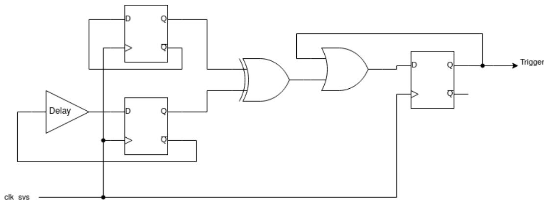
The detector triggers when the two D-flops take on different values, which is impossible under normal circumstances. The delay line is programmable from 75% to 120% of the minimum system clock period in increments of 15%. Higher delays make the circuit more sensitive to loss of setup margin. To configure initial sensitivity, use the
GLITCH_DETECTOR_SENS
OTP flags. You can fine-tune sensitivity for each detector using the
SENSITIVITY
register.
Because the circuit is constructed from digital standard cells, it closely tracks the changes in propagation delay to nearby cells caused by voltage and temperature fluctuations. Therefore the delay line's propagation delay is specified as a fraction of the maximum system clock data path delay, rather than a fixed time in nanoseconds.
10.9.2. Trigger response
When any of the detectors fires, the corresponding bit in the
TRIG_STATUS
is set. If the glitch detector block is armed, this detector event also resets almost all logic in the switched core domain. The glitch detector is armed if:
- • The
DISARMregister is not set to the disarming bit pattern, and at least one of the following is true:- ◦ The
GLITCH_DETECTOR_ENOTP flag was programmed some time before the most recent reset of the OTP block - ◦ The
ARMregister is set to an arming bit pattern
- ◦ The
This holds the majority of the switched core domain in reset for approximately 120 microseconds before releasing the reset. Specifically, this resets the PSM (Section 7.3), which resets all PSM-controlled resets starting with the processor cold reset domain, in addition to all blocks reset by the
RESETS
block, which is itself reset by the PSM. The detector circuits are also reset, as is the system watchdog including the watchdog scratch registers.
After a glitch detector-initiated reset, the
CHIP_RESET.HAD_GLITCH_DETECT
flag is set so that software can diagnose that the last reset was caused by a glitch detector trigger. Check the
TRIG_STATUS
register to see which detector fired. This can be useful for tuning the thresholds of individual detectors.
The only way to clear the detector circuits is to reset them, either via a full switched core domain reset (such as the
RUN
pin, the SW-DP reset request, a PoR/BoR reset, or a reset of the switched core domain configured by POWMAN controls), or by arming the glitch detector block so that the detectors reset along with the PSM.
Recovering from the glitch detector firing requires the low-power oscillator to be running (Section 8.4). Allowing the
glitch detectors to fire when the LPOSC is disabled results in the chip holding itself in reset indefinitely until an external reset such as the RUN pin resets the detectors.
10.9.3. List of registers
The glitch detector control registers start at an address of 0x40158000 .
Table 971. List of GLITCH_DETECTOR registers
| Offset | Name | Info |
|---|---|---|
| 0x00 | ARM | Forcibly arm the glitch detectors, if they are not already armed by OTP. When armed, any individual detector trigger will cause a restart of the switched core power domain's power-on reset state machine. Glitch detector triggers are recorded accumulatively in TRIG_STATUS. If the system is reset by a glitch detector trigger, this is recorded in POWMAN_CHIP_RESET. This register is Secure read/write only. |
| 0x04 | DISARM | |
| 0x08 | SENSITIVITY | Adjust the sensitivity of glitch detectors to values other than their OTP-provided defaults. This register is Secure read/write only. |
| 0x0c | LOCK | |
| 0x10 | TRIG_STATUS | Set when a detector output triggers. Write-1-clear. (May immediately return high if the detector remains in a failed state. Detectors can only be cleared by a full reset of the switched core power domain.) This register is Secure read/write only. |
| 0x14 | TRIG_FORCE | Simulate the firing of one or more detectors. Writing ones to this register will set the matching bits in STATUS_TRIG. If the glitch detectors are currently armed, writing ones will also immediately reset the switched core power domain, and set the reset reason latches in POWMAN_CHIP_RESET to indicate a glitch detector resets. This register is Secure read/write only. |
GLITCH_DETECTOR: ARM Register
Offset: 0x00
Table 972. ARM Register
| Bits | Description | Type | Reset |
|---|---|---|---|
| 31:16 | Reserved. | - | - |
| Bits | Description | Type | Reset |
|---|---|---|---|
| 15:0 | Forcibly arm the glitch detectors, if they are not already armed by OTP. When armed, any individual detector trigger will cause a restart of the switched core power domain's power-on reset state machine. Glitch detector triggers are recorded accumulatively in TRIG_STATUS. If the system is reset by a glitch detector trigger, this is recorded in POWMAN_CHIP_RESET. This register is Secure read/write only. | RW | 0x5bad |
| Enumerated values: | |||
| 0x5bad → NO: Do not force the glitch detectors to be armed | |||
| 0x0000 → YES: Force the glitch detectors to be armed. (Any value other than ARM_NO counts as YES) |
GLITCH_DETECTOR: DISARM Register
Offset: 0x04
Table 973. DISARM Register
| Bits | Description | Type | Reset |
|---|---|---|---|
| 31:16 | Reserved. | - | - |
| 15:0 | Forcibly disarm the glitch detectors, if they are armed by OTP. Ignored if ARM is YES. This register is Secure read/write only. | RW | 0x0000 |
| Enumerated values: | |||
| 0x0000 → NO: Do not disarm the glitch detectors. (Any value other than DISARM_YES counts as NO) | |||
| 0xdcaf → YES: Disarm the glitch detectors |
GLITCH_DETECTOR: SENSITIVITY Register
Offset: 0x08
Description
Adjust the sensitivity of glitch detectors to values other than their OTP-provided defaults.
This register is Secure read/write only.
Table 974. SENSITIVITY Register
| Bits | Description | Type | Reset |
|---|---|---|---|
| 31:24 | DEFAULT | RW | 0x00 |
| Enumerated values: | |||
| 0x00 → YES: Use the default sensitivity configured in OTP for all detectors. (Any value other than DEFAULT_NO counts as YES) | |||
| 0xde → NO: Do not use the default sensitivity configured in OTP. Instead use the value from this register. | |||
| 23:16 | Reserved. | - | - |
| 15:14 | DET3_INV : Must be the inverse of DET3, else the default value is used. | RW | 0x0 |
| 13:12 | DET2_INV : Must be the inverse of DET2, else the default value is used. | RW | 0x0 |
| Bits | Description | Type | Reset |
|---|---|---|---|
| 11:10 | DET1_INV : Must be the inverse of DET1, else the default value is used. | RW | 0x0 |
| 9:8 | DET0_INV : Must be the inverse of DET0, else the default value is used. | RW | 0x0 |
| 7:6 | DET3 : Set sensitivity for detector 3. Higher values are more sensitive. | RW | 0x0 |
| 5:4 | DET2 : Set sensitivity for detector 2. Higher values are more sensitive. | RW | 0x0 |
| 3:2 | DET1 : Set sensitivity for detector 1. Higher values are more sensitive. | RW | 0x0 |
| 1:0 | DET0 : Set sensitivity for detector 0. Higher values are more sensitive. | RW | 0x0 |
GLITCH_DETECTOR: LOCK Register
Offset: 0x0c
Table 975. LOCK Register
| Bits | Description | Type | Reset |
|---|---|---|---|
| 31:8 | Reserved. | - | - |
| 7:0 | Write any nonzero value to disable writes to ARM, DISARM, SENSITIVITY and LOCK. This register is Secure read/write only. | RW | 0x00 |
GLITCH_DETECTOR: TRIG_STATUS Register
Offset: 0x10
Description
Set when a detector output triggers. Write-1-clear.
(May immediately return high if the detector remains in a failed state. Detectors can only be cleared by a full reset of the switched core power domain.)
This register is Secure read/write only.
Table 976. TRIG_STATUS Register
| Bits | Description | Type | Reset |
|---|---|---|---|
| 31:4 | Reserved. | - | - |
| 3 | DET3 | WC | 0x0 |
| 2 | DET2 | WC | 0x0 |
| 1 | DET1 | WC | 0x0 |
| 0 | DET0 | WC | 0x0 |
GLITCH_DETECTOR: TRIG_FORCE Register
Offset: 0x14
Table 977.
TRIG_FORCE Register
| Bits | Description | Type | Reset |
|---|---|---|---|
| 31:4 | Reserved. | - | - |
| 3:0 | Simulate the firing of one or more detectors. Writing ones to this register will set the matching bits in STATUS_TRIG. If the glitch detectors are currently armed, writing ones will also immediately reset the switched core power domain, and set the reset reason latches in POWMAN_CHIP_RESET to indicate a glitch detector resets. This register is Secure read/write only. | SC | 0x0 |
10.10. Factory test JTAG
RP2350 contains JTAG hardware that is used to test devices after manufacturing. It is not a public interface, but its capabilities are documented here for user risk assessment.
Much like the user-facing SWD debug, the JTAG interface is disabled at power-on, and enabled only once the OTP power-on state machine has completed. If the CRIT1.SECURE_BOOT_ENABLE , CRIT1.SECURE_DEBUG_DISABLE or CRIT1.DEBUG_DISABLE flag is set, then the JTAG interface remains held in reset indefinitely, so it cannot be communicated with and cannot control internal hardware. The only way to re-enable the JTAG interface after setting one of these critical flags is to set the RMA OTP flag ( Section 10.11 ), which also permanently disables read and write access to user OTP pages. The RMA flag itself is write-protected using the page 63 protection flags, so you can prevent untrusted software from programming the RMA flag.
To take the JTAG interface out of reset, write to bit 0 of the RP-AP control register, accessed via SWD. To connect the JTAG interface to GPIOs ( TCK , TMS , TDI , TDO on GPIO0 → 3), set bit 1 of the RP-AP control register. The RP-AP is always accessible, even when external debug is disabled, because it is also used to enter the debug keys ( Section 3.5.9.2 ). However, attempts to remove the JTAG reset are ignored when any of the aforementioned critical OTP flags are set.
The JTAG interface provides:
- • Standard test capabilities such as IDCODE and EXTEST (boundary scan); these are not guaranteed to be IEEE-compliant, as this is an internal factory test interface, not a user-facing debug port
- • Full AHB bus access, with Secure and Privileged attributes and an HMASTER of 3 (debugger)
- • Asynchronous access to a small subset of register controls, generally limited to clocks, oscillators and reset controls
The JTAG interface's AHB bus access is muxed in place of the DMA read port, when the JTAG interface is enabled.
Any and all details of the factory test JTAG interface, with the exception of which OTP flags disable and re-enable it, are subject to change with revisions of the RP2350 silicon.
10.11. Decommissioning
Devices returned to Raspberry Pi Ltd for fault analysis must be decommissioned before return, to restore factory test functionality. A device is decommissioned by programming the OTP PAGE63_LOCK0.RMA flag to 1. Return may be requested by Raspberry Pi Ltd when diagnosing systematic issues across a population of devices.
Setting the RMA flag has two effects:
- • The factory test JTAG interface is re-enabled, irrespective of the values of any CRIT1 flags.
- • Pages 3 through 61 become permanently inaccessible: this is all pages that do not have predefined contents listed in Section 13.10 .
The effect on OTP contents is as though all had been promoted to the inaccessible lock level:
- • write attempts will fail
- • read attempts will return all-ones, when read via an unguarded read alias, or bus faults, when read via a guarded read alias
The logic that disables OTP access and the logic that re-enables the test interface are driven from the same signal internally, so this bit does not provide external access to user OTP contents, provided no sensitive material is stored in pages 0, 1, 2, 62 or 63. Setting the RMA flag is irreversible, and may render the device permanently unusable, if it is configured to boot from OTP contents stored in pages 3 through 61.
After setting the RMA flag, test the OTP access (e.g. via the SWD interface) and verify for yourself that any sensitive data stored in OTP has been made inaccessible.
The page 63 lock word has no other function besides RMA because pages 62/63 contain the lock words themselves, each of which is protected by its own permissions. This means the RMA flag can be write-protected by setting either a hard or soft lock on page 63.