11. PIO
11.1. Overview
RP2350 contains 3 identical PIO blocks. Each PIO block has dedicated connections to the bus fabric, GPIO and interrupt controller. The diagram for a single PIO block is shown below in Figure 44 .
Figure 44. PIO block-level diagram. There are three PIO blocks, each containing four state machines. The four state machines simultaneously execute programs from shared instruction memory. FIFO data queues buffer data transferred between PIO and the system. GPIO mapping logic allows each state machine to observe and manipulate up to 32 GPIOs.
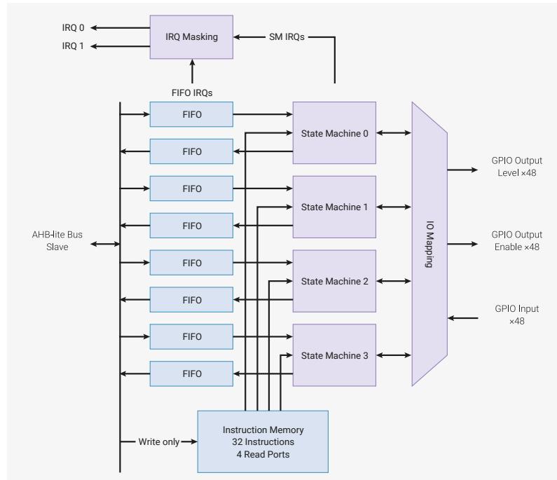
The programmable input/output block (PIO) is a versatile hardware interface. It can support a variety of IO standards, including:
- • 8080 and 6800 parallel bus
- • I2C
- • 3-pin I2S
- • SDIO
- • SPI, DSPI, QSPI
- • UART
- • DPI or VGA (via resistor DAC)
PIO is programmable in the same sense as a processor. There are three PIO blocks with four state machines. Each can independently execute sequential programs to manipulate GPIOs and transfer data. Unlike a general purpose processor, PIO state machines are specialised for IO, with a focus on determinism, precise timing, and close integration with fixed-function hardware. Each state machine is equipped with:
- • Two 32-bit shift registers (either direction, any shift count)
- • Two 32-bit scratch registers
- • 4 × 32-bit bus FIFO in each direction (TX/RX), reconfigurable as 8 × 32 in a single direction
- • Fractional clock divider (16 integer, 8 fractional bits)
- • Flexible GPIO mapping
- • DMA interface (sustained throughput up to 1 word per clock from system DMA)
- • IRQ flag set/clear/status
Each state machine, along with its supporting hardware, occupies approximately the same silicon area as a standard serial interface block, such as an SPI or I2C controller. However, PIO state machines can be configured and reconfigured dynamically to implement numerous different interfaces.
Making state machines programmable in a software-like manner, rather than a fully configurable logic fabric like a complex programmable logic device (CPLD), allows more hardware interfaces to be offered in the same cost and power envelope. This also presents a more familiar programming model, and simpler tool flow, to those who wish to exploit PIO's full flexibility by programming it directly, rather than using a pre-made interface from the PIO library.
PIO is performant as well as flexible, thanks to a carefully selected set of fixed-function hardware inside each state machine. When outputting DPI, PIO can sustain 360 Mb/s during the active scanline period when running from a 48 MHz system clock. In this example, one state machine handles frame/scanline timing and generates the pixel clock. Another handles the pixel data and unpacks run-length-encoded scanlines.
State machines' inputs and outputs are mapped to up to 32 GPIOs (limited to 30 GPIOs for RP2350). All state machines have independent, simultaneous access to any GPIO. For example, the standard UART code allows TX , RX , CTS and RTS to be any four arbitrary GPIOs, and I2C permits the same for SDA and SCL . The amount of freedom available depends on how exactly a given PIO program chooses to use PIO's pin mapping resources, but at the minimum, an interface can be freely shifted up or down by some number of GPIOs.
11.1.1. Changes from RP2040
RP2350 adds the following new registers and controls:
- •
DBG_CFGINFO.VERSION
indicates the PIO version, to allow PIO feature detection at runtime.
- ◦ This 4-bit field was reserved-0 on RP2040 (indicating version 0), and reads as 1 on RP2350.
- •
GPIOBASE
adds support for more than 32 GPIOs per PIO block.
- ◦ Each PIO block is still limited to 32 GPIOs at a time, but GPIOBASE selects which 32.
- •
CTRL.NEXT_PIO_MASK
and
CTRL.PREV_PIO_MASK
apply some
CTRL
register operations to state machines in neighbouring PIO blocks simultaneously.
- ◦ CTRL.NEXTPREV_SM_DISABLE stops PIO state machines in multiple PIO blocks simultaneously.
- ◦ CTRL.NEXTPREV_SM_ENABLE starts PIO state machines in multiple PIO blocks simultaneously.
- ◦ CTRL.NEXTPREV_CLKDIV_RESTART synchronises the clock dividers of PIO state machines in multiple PIO blocks
- •
SM0_SHIFTCTRL.IN_COUNT
masks unneeded IN-mapped pins to zero.
- ◦ This is useful for MOV x, PINS instructions, which previously always returned a full rotated 32-bit value.
- • IRQ0_INTE and IRQ1_INTE now expose all eight SM IRQ flags to system-level interrupts (not just the lower four).
- • Registers starting from
RXF0_PUTGET0
expose each RX FIFO's internal storage registers for random read or write access from the system,
- ◦ The new FJOIN_RX_PUT FIFO join mode enables random writes from the state machine, and random reads from the system (for implementing status registers).
- ◦ The new FJOIN_RX_GET FIFO join mode enables random reads from the state machine, and random writes from the system (for implementing control registers).
- ◦ Setting both FJOIN_RX_PUT and FJOIN_RX_GET enables random read and write access from the state machine, but disables system access.
RP2350 adds the following new instruction features:
- • Adds
PINCTRL_JMP_PINas a source for theWAITinstruction, plus an offset in the range 0-3.- ◦ This gives
WAITpin arguments a per-SM mapping that is independent of the IN-mapped pins.
- ◦ This gives
- • Adds
PINDIRSas a destination forMOV.- ◦ This allows changing the direction of all OUT-mapped pins with a single instruction:
MOV PINDIRS, NULLorMOV PINDIRS, ~NULL
- ◦ This allows changing the direction of all OUT-mapped pins with a single instruction:
- • Adds SM IRQ flags as a source for
MOV x, STATUS- ◦ This allows branching (as well as blocking) on the assertion of SM IRQ flags.
- • Extends
IRQinstruction encoding to allow state machines to set, clear and observe IRQ flags from different PIO blocks.- ◦ There is no delay penalty for cross-PIO IRQ flags: an
IRQon one state machine is observable to all state machines on the next cycle.
- ◦ There is no delay penalty for cross-PIO IRQ flags: an
- • Adds the
FJOIN_RX_GETFIFO mode.- ◦ A new
MOVencoding reads any of the four RX FIFO storage registers intoOSR. - ◦ This instruction permits random reads of the four FIFO entries, indexed either by instruction bits or the
Yscratch register.
- ◦ A new
- • Adds the
FJOIN_RX_PUTFIFO mode.- ◦ A new
MOVencoding writes theISRinto any of the four RX FIFO storage registers. - ◦ The registers are indexed either by instruction bits or the
Yscratch register.
- ◦ A new
RP2350 adds the following security features:
- • Limits Non-secure PIOs (set to via
ACCESSCTRL) to observation of only Non-secure GPIOs. Attempting to read a Secure GPIO returns a 0. - • Disables cross-PIO functionality (IRQs,
CTRL_NEXTPREVoperations) between Non-secure PIO blocks (those which permit Non-secure access according toACCESSCTRL) and Secure-only blocks (those which do not).
RP2350 includes the following general improvements:
- • Increased the number of PIO blocks from two to three (8 → 12 state machines).
- • Improved GPIO input/output delay and skew.
- • Reduced DMA request (DREQ) latency by one cycle vs RP2040.
11.2. Programmer's model
The four state machines execute from shared instruction memory. System software loads programs into this memory, configures the state machines and IO mapping, and then sets the state machines running. PIO programs come from various sources: assembled directly by the user, drawn from the PIO library, or generated programmatically by user software.
From this point on, state machines are generally autonomous, and system software interacts through DMA, interrupts and control registers, as with other peripherals on RP2350. For more complex interfaces, PIO provides a small but flexible set of primitives which allow system software to be more hands-on with state machine control flow.
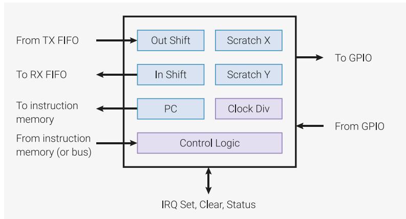
Figure 45. State machine overview. Data flows in and out through a pair of FIFOs. The state machine executes a program which transfers data between these FIFOs, a set of internal registers, and the pins. The clock divider can reduce the state machine's execution speed by a constant factor.
11.2.1. PIO programs
PIO state machines execute short binary programs.
Programs for common interfaces, such as UART, SPI, or I2C, are available in the PIO library. In many cases, it is not necessary to write PIO programs. However, the PIO is much more flexible when programmed directly, supporting a wide variety of interfaces which may not have been foreseen by its designers.
The PIO has a total of nine instructions: JMP , WAIT , IN , OUT , PUSH , PULL , MOV , IRQ , and SET . For more information about these instructions, see Section 11.4 .
Though the PIO only has a total of nine instructions, it would be difficult to edit PIO program binaries by hand. PIO assembly is a textual format, describing a PIO program, where each command corresponds to one instruction in the output binary. The following code snippet contains an example program written in in PIO assembly:
Pico Examples: https://github.com/raspberrypi/pico-examples/blob/master/pio/squarewave/squarewave.pio Lines 8 - 13
8 .program squarewave
9   set pindirs, 1   ; Set pin to output
10 again:
11   set pins, 1 [1] ; Drive pin high and then delay for one cycle
12   set pins, 0     ; Drive pin low
13   jmp again       ; Set PC to label `again`
The PIO assembler is included with the SDK, and is called pioasm . This program processes a PIO assembly input text file, which may contain multiple programs, and writes out the assembled programs ready for use. For the SDK, these assembled programs are emitted as C headers, containing constant arrays.
For more information, see Section 11.3 .
11.2.2. Control flow
On every system clock cycle, each state machine fetches, decodes and executes one instruction. Each instruction takes precisely one cycle, unless it explicitly stalls (such as the WAIT instruction). Instructions may insert a delay of up to 31 cycles before the next instruction execute, to help write cycle-exact programs.
The program counter, or PC , points to the location in the instruction memory being executed on this cycle. Generally, PC increments by one each cycle, wrapping at the end of the instruction memory. Jump instructions are an exception and explicitly provide the next value that PC will take.
Our example assembly program (listed as .program squarewave above) shows both of these concepts in practice. It drives a 50/50 duty cycle square wave with a period of four cycles onto a GPIO. Using some other features (e.g. side-set) this can be made as low as two cycles.
NOTESide-set is where a state machine drives a small number of GPIOs in addition to the main side effects of the instruction it executes. It's described fully in Section 11.5.1 .
The system has write-only access to the instruction memory, which is used to load programs. The clock divider slows the state machine's execution by a constant factor, represented as a 16.8 fixed-point fractional number. In the following example, if a clock division of 2.5 were programmed, the square wave would have a period of \( 4 \times 2.5 = 10 \) cycles. This is useful for setting a precise baud rate for a serial interface, such as a UART.
Pico Examples: https://github.com/raspberrypi/pico-examples/blob/master/pio/squarewave/squarewave.c Lines 34 - 38
34 // Load the assembled program directly into the PIO's instruction memory.
35 // Each PIO instance has a 32-slot instruction memory, which all 4 state
36 // machines can see. The system has write-only access.
37 for (uint i = 0; i < count_of(squarewave_program_instructions); ++i)
38     pio->instr_mem[i] = squarewave_program_instructions[i];
The following code fragments are part of a complete code example which drives a 12.5 MHz square wave out of GPIO 0 (or any other pins we might choose to map). We can also use pins WAIT PIN instruction to stall a state machine's execution for some amount of time, or a JMP PIN instruction to branch on the state of a pin, so control flow can vary based on pin state.
Pico Examples: https://github.com/raspberrypi/pico-examples/blob/master/pio/squarewave/squarewave.c Lines 42 - 47
42 // Configure state machine 0 to run at sysclk/2.5. The state machines can
43 // run as fast as one instruction per clock cycle, but we can scale their
44 // speed down uniformly to meet some precise frequency target, e.g. for a
45 // UART baud rate. This register has 16 integer divisor bits and 8
46 // fractional divisor bits.
47 pio->sm[0].clkdiv = (uint32_t) (2.5f * (1 << 16));
Pico Examples: https://github.com/raspberrypi/pico-examples/blob/master/pio/squarewave/squarewave.c Lines 51 - 59
51 // There are five pin mapping groups (out, in, set, side-set, jmp pin)
52 // which are used by different instructions or in different circumstances.
53 // Here we're just using SET instructions. Configure state machine 0 SETs
54 // to affect GPIO 0 only; then configure GPIO0 to be controlled by PIO0,
55 // as opposed to e.g. the processors.
56 pio->sm[0].pinctrl =
57     (1 << PIO_SM0_PINCTRL_SET_COUNT_LSB) |
58     (0 << PIO_SM0_PINCTRL_SET_BASE_LSB);
59 gpio_set_function(0, pio_get_funcsel(pio));
The system can start and stop each state machine at any time, via the CTRL register. Multiple state machines can be started simultaneously, and the deterministic nature of PIO means they can stay perfectly synchronised.
Pico Examples: https://github.com/raspberrypi/pico-examples/blob/master/pio/squarewave/squarewave.c Lines 63 - 67
63 // Set the state machine running. The PIO CTRL register is global within a
64 // PIO instance, so you can start/stop multiple state machines
65 // simultaneously. We're using the register's hardware atomic set alias to
66 // make one bit high without doing a read-modify-write on the register.
67 hw_set_bits(&pio->ctrl, 1 << (PIO_CTRL_SM_ENABLE_LSB + 0));
Most instructions are executed from instruction memory, but there are other sources which can be freely mixed:
- • Instructions written to a special configuration register ( SMx INSTR ) are immediately executed, momentarily interrupting other execution. For example, a JMP instruction written to SMx INSTR causes the state machine to start executing from a different location.
- • Instructions can be executed from a register, using the MOV EXEC instruction.
- • Instructions can be executed from the output shifter, using the OUT EXEC instruction
The last of these is particularly versatile: instructions can be embedded in the stream of data passing through the FIFO. The I2C example uses this to embed e.g. STOP and RESTART line conditions alongside normal data. In the case of MOV and OUT EXEC , the MOV/OUT itself executes in one cycle, and the executee on the next.
11.2.3. Registers
Each state machine possesses a small number of internal registers. These hold input or output data, and temporary values such as loop counter variables.
11.2.3.1. Output Shift Register (OSR)
Figure 46. Output Shift Register (OSR). Data is parcelled out 1...32 bits at a time, and unused data is recycled by a bidirectional shifter. Once empty, the OSR is reloaded from the TX FIFO.
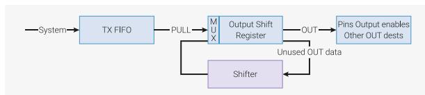
The Output Shift Register (OSR) holds and shifts output data between the TX FIFO and the pins or other destinations, such as the scratch registers.
- • PULL instructions: remove a 32-bit word from the TX FIFO and place into the OSR.
- • OUT instructions shift data from the OSR to other destinations, 1...32 bits at a time.
- • The OSR fills with zeroes as data is shifted out
- • The state machine will automatically refill the OSR from the FIFO on an OUT instruction, once some total shift count threshold is reached, if autopull is enabled
- • Shift direction can be left/right, configurable by the processor via configuration registers
For example, to stream data through the FIFO and output to the pins at a rate of one byte per two clocks:
1 .program pull_example1
2 loop:
3     out pins, 8
4 public entry_point:
5     pull
6     out pins, 8 [1]
7     out pins, 8 [1]
8     out pins, 8
9     jmp loop
11.2.4. Autopull
Autopull (see Section 11.5.4 ) allows the hardware to automatically refill the OSR in the majority of cases, with the state machine stalling if it tries to OUT from an empty OSR. This has two benefits:
- • No instructions spent on explicitly pulling from FIFO at the right time
- • Higher throughput: can output up to 32 bits on every single clock cycle, if the FIFO stays topped up
After configuring autopull, the above program can be simplified to the following, which behaves identically:
1 .program pull_example2
2
3 loop:
4     out pins, 8
5 public entry_point:
6     jmp loop
Program wrapping ( Section 11.5.2 ) allows further simplification and, if desired, an output of 1 byte every system clock cycle.
1 .program pull_example3
2
3 public entry_point:
4     .wrap_target
5     out pins, 8 [1]
6     .wrap
11.2.4.1. Input Shift Register (ISR)
Figure 47. Input Shift Register (ISR). Data enters 1...32 bits at a time, and current contents is shifted left or right to make room. Once full, contents is written to the RX FIFO.

graph LR
    Pins[Pins Other IN sources] --> Shifter[Shifter]
    Shifter -- IN --> ISR[Input Shift Register]
    ISR -- PUSH --> RXFIFO[RX FIFO]
    RXFIFO --> System[System]
    ISR -- "From previous INs" --> Shifter
- • IN instructions shift 1...32 bits at a time into the register.
- • PUSH instructions write the ISR contents to the RX FIFO.
- • The ISR is cleared to all-zeroes when pushed.
- • The state machine will automatically push the ISR on an IN instruction, once some shift threshold is reached, if autopush is enabled.
- • Shift direction is configurable by the processor via configuration registers
Some peripherals, like UARTs, must shift in from the left to get correct bit order, since the wire order is LSB-first; however, the processor may expect the resulting byte to be right-aligned. This is solved by the special null input source, which allows the programmer to shift some number of zeroes into the ISR, following the data.
11.2.4.2. Shift counters
State machines remember how many bits, in total, have been shifted out of the OSR via OUT instructions, and into the ISR via IN instructions. This information is tracked at all times by a pair of hardware counters: the output shift counter and the input shift counter. Each is capable of holding values from 0 to 32 inclusive. With each shift operation, the relevant counter increments by the shift count, up to the maximum value of 32 (equal to the width of the shift register). The state machine can be configured to perform certain actions when a counter reaches a configurable threshold:
- • The OSR can be automatically refilled once some number of bits have been shifted out (see Section 11.5.4 ).
- • The ISR can be automatically emptied once some number of bits have been shifted in (see Section 11.5.4 ).
- • PUSH or PULL instructions can be conditioned on the input or output shift counter, respectively.
On PIO reset, or the assertion of CTRL_SM_RESTART , the input shift counter is cleared to 0 (nothing yet shifted in), and the output shift counter is initialised to 32 (nothing remaining to be shifted out; fully exhausted). Some other instructions affect the shift counters:
- • A successful PULL clears the output shift counter to 0
- • A successful PUSH clears the input shift counter to 0
- • MOV OSR, ... (i.e. any MOV instruction that writes OSR ) clears the output shift counter to 0
- • MOV ISR, ... (i.e. any MOV instruction that writes ISR ) clears the input shift counter to 0
- • OUT ISR, count sets the input shift counter to count
11.2.4.3. Scratch registers
Each state machine has two 32-bit internal scratch registers, called X and Y .
They are used as:
- • Source/destination for IN/OUT/SET/MOV
- • Source for branch conditions
For example, suppose we wanted to produce a long pulse for "1" data bits, and a short pulse for "0" data bits:
1 .program ws2812_led
2
3 public entry_point:
4     pull
5     set x, 23          ; Loop over 24 bits
6 bitloop:
7     set pins, 1        ; Drive pin high
8     out y, 1 [5]       ; Shift 1 bit out, and write it to y
9     jmp !y skip        ; Skip the extra delay if the bit was 0
10    nop [5]
11 skip:
12    set pins, 0 [5]
13    jmp x-- bitloop ; Jump if x nonzero, and decrement x
14    jmp entry_point
Here X is used as a loop counter, and Y is used as a temporary variable for branching on single bits from the OSR. This program can be used to drive a WS2812 LED interface, although more compact implementations are possible (as few as 3 instructions).
MOV allows the use of the scratch registers to save/restore the shift registers if, for example, you would like to repeatedly shift out the same sequence.
i NOTE
A much more compact WS2812 example (4 instructions total) is shown in Section 11.6.2 .
11.2.4.4. FIFOs
Each state machine has a pair of 4-word deep FIFOs, one for data transfer from system to state machine (TX), and the other for state machine to system (RX). The TX FIFO is written to by system bus masters, such as a processor or DMA controller, and the RX FIFO is written to by the state machine. FIFOs decouple the timing of the PIO state machines and the system bus, allowing state machines to go for longer periods without processor intervention.
FIFOs also generate data request (DREQ) signals, which allow a system DMA controller to pace its reads/writes based on the presence of data in an RX FIFO, or space for new data in a TX FIFO. This allows a processor to set up a long transaction, potentially involving many kilobytes of data, which will proceed with no further processor intervention.
Often, a state machine only transfers data in one direction. In this case, the
SHIFTCTRL_FJOIN
option can merge the two FIFOs into a single 8-entry FIFO that only goes in one direction. This is useful for high-bandwidth interfaces such as DPI.
11.2.5. Stalling
State machines may momentarily pause execution for a number of reasons:
- • A
WAITinstruction's condition is not yet met - • A blocking
PULLwhen the TX FIFO is empty, or a blockingPUSHwhen the RX FIFO is full - • An
IRQ WAITinstruction which has set anIRQflag, and is waiting for it to clear - • An
OUTinstruction when autopull is enabled, and OSR has already reached its shift threshold - • An
INinstruction when autopush is enabled, ISR reaches its shift threshold, and the RX FIFO is full
In this case, the program counter does not advance, and the state machine will continue executing this instruction on the next cycle. If the instruction specifies some number of delay cycles before the next instruction starts, these do not begin until after the stall clears.
i NOTE
Side-set ( Section 11.5.1 ) is not affected by stalls, and always takes place on the first cycle of the attached instruction.
11.2.6. Pin mapping
PIO controls the output level and direction of up to 32 GPIOs, and can observe their input levels. On every system clock cycle, each state machine may do none, one, or both of the following:
- • Change the level or direction of some GPIOs via an
OUTorSETinstruction, or read some GPIOs via anINinstruction - • Change the level or direction of some GPIOs via a side-set operation
Each of these operations uses one of four contiguous ranges of GPIOs, with the base and count of each range configured via each state machine's
PINCTRL
register. There is a range for each of
OUT
,
SET
,
IN
and side-set operations. Each range can cover any of the GPIOs accessible to a given PIO block (on RP2350 this is the 30 user GPIOs), and the ranges can overlap.
For each individual GPIO output (level and direction separately), PIO considers all 8 writes that may have occurred on that cycle, and applies the write from the highest-numbered state machine. If the same state machine performs a
SET
/
OUT
and a side-set on the same GPIO simultaneously, the side-set is used. If no state machine writes to this GPIO output, its value does not change from the previous cycle.
Generally each state machine's outputs are mapped to a distinct group of GPIOs, implementing some peripheral interface.
11.2.7. IRQ flags
IRQ flags are state bits which can be set or cleared by state machines or the system. There are 8 in total: all 8 are visible to all state machines, and the lower 4 can also be masked into one of PIO's interrupt request lines, via the
IRQ0_INTE
and
IRQ1_INTE
control registers.
They have two main uses:
- • Asserting system level interrupts from a state machine program, and optionally waiting for the interrupt to be acknowledged
- • Synchronising execution between two state machines
State machines interact with the flags via the
IRQ
and
WAIT
instructions.
11.2.8. Interactions between state machines
Instruction memory is implemented as a 1-write, 4-read register file, allowing all four state machines to read an instruction on the same cycle without stalling.
There are three ways to apply the multiple state machines:
- • Pointing multiple state machines at the same program
- • Pointing multiple state machines at different programs
- • Using multiple state machines to run different parts of the same interface, e.g. TX and RX side of a UART, or clock/hsync and pixel data on a DPI display
State machines cannot communicate data, but they can synchronise with one another by using the IRQ flags. There are 8 flags total. Each state machine can set or clear any flag using the
IRQ
instruction, and can wait for a flag to go high or low using the
WAIT IRQ
instruction. This allows cycle-accurate synchronisation between state machines.
11.3. PIO assembler (pioasm)
The PIO Assembler parses a PIO source file and outputs the assembled version ready for inclusion in an RP2350 application. This includes C and C++ applications built against the SDK, and Python programs running on the RP2350 MicroPython port.
This section briefly introduces the directives and instructions that can be used in
pioasm
input. For a deeper discussion of how to use
pioasm
, how it is integrated into the SDK build system, extended features such as code pass through, and the various output formats it can produce, see
Raspberry Pi Pico-series C/C++ SDK
.
11.3.1. Directives
The following directives control the assembly of PIO programs:
.define (PUBLIC) <symbol> <value>
Define an integer symbol named
<symbol>
with the value
<value>
(see
Section 11.3.2
). If this
.define
appears before the first program in the input file, then this define is global to all programs, otherwise it is local to the program in which it occurs. If
PUBLIC
is specified, the symbol will be emitted into the assembled output for use by user code. For the SDK this takes the following forms:
- •
#define <program_name> <symbol> value:for program symbols - •
#define <symbol> value:for global symbols
.clock_div <divider>
If this directive is present,
<divider>
is the state machine clock divider for the program. Note, that divider is a floating point value, but
may not
currently use arithmetic expressions or defined values. This directive affects the default state machine configuration for a program. This directive is only valid within a program before the first instruction.
.fifo <fifo_config>
If this directive is present, it is used to specify the FIFO configuration for the program. It affects the default state machine configuration for a program, but also restricts what instructions may be used (for example PUSH makes
no sense if there is no IN FIFO configured).
This directive supports the following configuration values:
- •
txrx: 4 FIFO entries for each of TX and RX; this is the default. - •
tx: All 8 FIFO entries for TX. - •
rx: All 8 FIFO entries for RX. - •
txput: 4 FIFO entries for TX, and 4 FIFO entries formov rxfifo[index], israkaput. This value is not supported on PIO version 0. - •
txget: 4 FIFO entries for TX, and 4 FIFO entries formov osr, rxfifo[index]akaget. This value is not supported on PIO version 0. - •
putget: 4 FIFO entries formov rxfifo[index], israkaput, and 4 FIFO entries formov osr, rxfifo[index]akaget. This value is not supported on PIO version 0.
This directive is only valid within a program before the first instruction.
.mov_status rxfifo < <n>.mov_status txfifo < <n>.mov_status irq <(prev|next)> set <n>This directive configures the source for the
mov
,
STATUS
. One of the three syntaxes can be used to set the status based on the RXFIFO level being below a value N, the TXFIFO level being below a value N, or an IRQ flag N being set on this PIO instance (or the next lower numbered, or higher numbered PIO instance if
prev
or
next
or specified). Note, that the IRQ option requires PIO version 1.
This directive affects the default state machine configuration for a program. This directive is only valid within a program before the first instruction.
.in <count> (left|right) (auto) (<threshold>)If this directive is present,
<count>
indicates the number of IN bits to be used. 'left' or 'right' if specified, control the ISR shift direction; 'auto', if present, enables "auto-push";
<threshold>
, if present, specifies the "auto-push" threshold. This directive affects the default state machine configuration for a program.
This directive is only valid within a program before the first instruction. When assembling for PIO version 0,
<count>
must be 32.
.program <name>Start a new program with the name
<name>
. Note that that name is used in code so should be alphanumeric/underscore not starting with a digit. The program lasts until another
.program
directive or the end of the source file. PIO instructions are only allowed within a program.
.origin <offset>Optional directive to specify the PIO instruction memory offset at which the program must load. Most commonly this is used for programs that must load at offset 0, because they use data based Jumps with the (absolute) jump target being stored in only a few bits. This directive is invalid outside a program.
.out <count> (left|right) (auto) (<threshold>)If this directive is present,
<count>
indicates the number of OUT bits to be used. 'left' or 'right' if specified control the OSR shift direction; 'auto', if present, enables "auto-pull";
<threshold>
, if present, specifies the "auto-pull" threshold. This directive affects the default state machine configuration for a program. This directive is only valid within a program before the first instruction.
.pio_version <version>This directive sets the target PIO hardware version. The version for RP2350 is 1 or
RP2350
, and is also the default version number. For backwards compatibility with RP2040, 0 or
RP2040
may be used.
If this directive appears before the first program in the input file, then this define is the default for all programs, otherwise it specifies the version for the program in which it occurs. If specified for a program, it must occur before the first instruction.
.set <count>
If this directive is present, <count> indicates the number of SET bits to be used. This directive affects the default state machine configuration for a program. This directive is only valid within a program before the first instruction.
.side_set <count> (opt) (pindirs)
If this directive is present, <count> indicates the number of side-set bits to be used. Additionally, opt may be specified to indicate that a side <value> is optional for instructions (note this requires stealing an extra bit – in addition to the <count> bits – from those available for the instruction delay). Finally, pindirs may be specified to indicate that the side set values should be applied to the PINDIRs and not the PINs. This directive is only valid within a program before the first instruction.
.wrap_target
Place prior to an instruction, this directive specifies the instruction where execution continues due to program wrapping. This directive is invalid outside of a program, may only be used once within a program, and if not specified defaults to the start of the program.
.wrap
Placed after an instruction, this directive specifies the instruction after which, in normal control flow (i.e. jmp with false condition, or no jmp ), the program wraps (to .wrap_target instruction). This directive is invalid outside of a program, may only be used once within a program, and if not specified defaults to after the last program instruction.
.lang_opt <lang> <name> <option>
Specifies an option for the program related to a particular language generator. (See Language Generators in Raspberry Pi Pico-series C/C++ SDK ). This directive is invalid outside of a program.
.word <value>
Stores a raw 16-bit value as an instruction in the program. This directive is invalid outside of a program.
11.3.2. Values
The following types of values can be used to define integer numbers or branch targets:
Table 978. Values in pioasm, i.e. <value>
| integer | An integer value, e.g. 3 or -7. |
| hex | A hexadecimal value, e.g. 0xf. |
| binary | A binary value, e.g. 0b1001. |
| symbol | A value defined by a .define (see pioasm_define). |
| <label> | The instruction offset of the label within the program. Typically used with a JMP instruction (see Section 11.4.2). |
| (<expression>) | An expression to be evaluated; see expressions. Note that the parentheses are necessary. |
11.3.3. Expressions
Expressions may be freely used within pioasm values.
Table 979. Expressions in pioasm i.e. <expression>
| <expression> + <expression> | The sum of two expressions |
| <expression> - <expression> | The difference of two expressions |
| <expression> * <expression> | The multiplication of two expressions |
| <expression> / <expression> | The integer division of two expressions |
| - <expression> | The negation of another expression |
| <expression> << <expression> | One expression shifted left by another expression |
| <expression> >> <expression> | One expression shifted right by another expression |
| :: <expression> | The bit reverse of another expression |
| <value> | Any value (see Section 11.3.2 ) |
11.3.4. Comments
To create a line comment that ignores all content on a certain line following a certain symbol, use
//
or
;
.
To create a C-style block comment that ignores all content across multiple lines until after a start symbol until an end symbol appears, use
/*
to begin the comment and
*/
to end the comment.
11.3.5. Labels
Labels use the following forms at the start of a line:
<symbol>:
PUBLIC <symbol>:
 TIP
TIPA label is really just an automatic
.define
with a value set to the current program instruction offset. A
PUBLIC
label is exposed to the user code in the same way as a
PUBLIC .define
.
11.3.6. Instructions
All pioasm instructions follow a common pattern:
<instruction> (side <side_set_value>) ([<delay_value>])
where:
<instruction>
<side_set_value>
An assembly instruction detailed in the following sections. (see Section 11.4 )
A value (see Section 11.3.2 ) to apply to the side_set pins at the start of the instruction. Note that the rules for a side-set value via
side <side_set_value>are dependent on the.side_set(seepioasm_side_set) directive for the program. If no.side_setis specified then theside <side_set_value>is invalid, if an optional number of sideset pins is specified thenside <side_set_value>may be present, and if a non-optional number of sideset pins is specified, thenside <side_set_value>is required. The<side_set_value>must fit within the number of side-set bits specified in the.side_setdirective.
<delay_value>
Specifies the number of cycles to delay after the instruction completes. The
delay_value
is specified as a value (see
Section 11.3.2
), and in general is between 0 and 31 inclusive (a 5-bit value), however the number of bits is reduced when sideset is enabled via the
.side_set
(see
pioasm_side_set
) directive. If the
<delay_value>
is not present, then the instruction has no delay.
NOTE
pioasm instruction names, keywords and directives are case insensitive; lower case is used in the Assembly Syntax sections below, as this is the style used in the SDK.
NOTE
Commas appear in some
Assembly Syntax
sections below, but are entirely optional, e.g.
out pins, 3
may be written
out pins 3
, and
jmp x-- label
may be written as
jmp x--, label
. The
Assembly Syntax
sections below uses the first style in each case as this is the style used in the SDK.
11.3.7. Pseudo-instructions
pioasm provides aliases for certain instructions, as a convenience:
nop
Assembles to
mov y, y
. No side effect, but a useful vehicle for a side-set operation or an extra delay.
11.4. Instruction Set
11.4.1. Summary
PIO instructions are 16 bits long, and use the following encoding:
Table 980. PIO instruction encoding
| Bit | 15 | 14 | 13 | 12 | 11 | 10 | 9 | 8 | 7 | 6 | 5 | 4 | 3 | 2 | 1 | 0 |
|---|---|---|---|---|---|---|---|---|---|---|---|---|---|---|---|---|
| JMP | 0 | 0 | 0 | Delay/side-set | Condition | Address | ||||||||||
| WAIT | 0 | 0 | 1 | Delay/side-set | Pol | Source | Index | |||||||||
| IN | 0 | 1 | 0 | Delay/side-set | Source | Bit count | ||||||||||
| OUT | 0 | 1 | 1 | Delay/side-set | Destination | Bit count | ||||||||||
| PUSH | 1 | 0 | 0 | Delay/side-set | 0 | IfF | Blk | 0 | 0 | 0 | 0 | 0 | ||||
| MOV | 1 | 0 | 0 | Delay/side-set | 0 | 0 | 0 | 1 | IdxI | 0 | Index | |||||
| PULL | 1 | 0 | 0 | Delay/side-set | 1 | IfE | Blk | 0 | 0 | 0 | 0 | 0 | ||||
| MOV | 1 | 0 | 0 | Delay/side-set | 1 | 0 | 0 | 1 | IdxI | 0 | Index | |||||
| MOV | 1 | 0 | 1 | Delay/side-set | Destination | Op | Source | |||||||||
| IRQ | 1 | 1 | 0 | Delay/side-set | 0 | Clr | Wait | IdxMode | Index | |||||||
| SET | 1 | 1 | 1 | Delay/side-set | Destination | Data | ||||||||||
All PIO instructions execute in one clock cycle.
The function of the 5-bit
Delay/side-set
field depends on the state machine's
SIDASET_COUNT
configuration:
- Up to 5 LSBs (5 minus
SIDASET_COUNT) encode a number of idle cycles inserted between this instruction and the next.
- • Up to 5 MSBs, set by
SIDASET_COUNT, encode a side-set (Section 11.5.1), which can assert a constant onto some GPIOs, concurrently with main instruction execution.
11.4.2. JMP
11.4.2.1. Encoding
| Bit | 15 | 14 | 13 | 12 | 11 | 10 | 9 | 8 | 7 | 6 | 5 | 4 | 3 | 2 | 1 | 0 |
|---|---|---|---|---|---|---|---|---|---|---|---|---|---|---|---|---|
| JMP | 0 | 0 | 0 | Delay/side-set | Condition | Address | ||||||||||
11.4.2.2. Operation
Set program counter to
Address
if
Condition
is true, otherwise no operation.
Delay cycles on a
JMP
always take effect, whether
Condition
is true or false, and they take place
after
Condition
is evaluated and the program counter is updated.
- • Condition:
- ◦ 000: (no condition) : Always
- ◦ 001:
!X: scratch X zero - ◦ 010:
X--: scratch X non-zero, prior to decrement - ◦ 011:
!Y: scratch Y zero - ◦ 100:
Y--: scratch Y non-zero, prior to decrement - ◦ 101:
X!=Y: scratch X not equal scratch Y - ◦ 110:
PIN: branch on input pin - ◦ 111:
!OSRE: output shift register not empty
- • Address: Instruction address to jump to. In the instruction encoding this is an absolute address within the PIO instruction memory
JMP PIN
branches on the GPIO selected by
EXECCTRL_JMP_PIN
, a configuration field which selects one out of the maximum of 32 GPIO inputs visible to a state machine, independently of the state machine’s other input mapping. The branch is taken if the GPIO is high.
!OSRE
compares the bits shifted out since the last
PULL
with the shift count threshold configured by
SHIFTCTRL_PULL_THRESH
. This is the same threshold used by autopull (Section 11.5.4).
JMP X--
and
JMP Y--
always decrement scratch register X or Y, respectively. The decrement is not conditional on the current value of the scratch register. The branch is conditioned on the
initial
value of the register, i.e. before the decrement took place: if the register is initially nonzero, the branch is taken.
11.4.2.3. Assembler syntax
jmp (<cond>) <target>
where:
- <cond>
An optional condition listed above (e.g.
!xfor scratch X zero). If a condition code is not specified, the branch is always taken. - <target>
A program label or value (see
Section 11.3.2
) representing instruction offset within the program (the first instruction being offset 0). Because the PIO JMP instruction uses absolute addresses in the PIO instruction memory, JMPs need to be adjusted based on the program load offset at runtime. This is handled for you when loading a program with the SDK, but care should be taken when encoding JMP instructions for use by
OUT EXEC.
11.4.3. WAIT
11.4.3.1. Encoding
| Bit | 15 | 14 | 13 | 12 | 11 | 10 | 9 | 8 | 7 | 6 | 5 | 4 | 3 | 2 | 1 | 0 |
|---|---|---|---|---|---|---|---|---|---|---|---|---|---|---|---|---|
| WAIT | 0 | 0 | 1 | Delay/side-set | Pol | Source | Index | |||||||||
11.4.3.2. Operation
Stall until some condition is met.
Like all stalling instructions ( Section 11.2.5 ), delay cycles begin after the instruction completes . That is, if any delay cycles are present, they do not begin counting until after the wait condition is met.
- • Polarity:
- ◦ 1: wait for a 1.
- ◦ 0: wait for a 0.
- • Source: what to wait on. Values are:
- ◦ 00: GPIO : System GPIO input selected by Index . This is an absolute GPIO index, and is not affected by the state machine's input IO mapping.
- ◦ 01: PIN : Input pin selected by Index . This state machine's input IO mapping is applied first, and then Index selects which of the mapped bits to wait on. In other words, the pin is selected by adding Index to the PINCTRL_IN_BASE configuration, modulo 32.
- ◦ 10: IRQ : PIO IRQ flag selected by Index
- ◦ 11: JMPPIN : wait on the pin indexed by the PINCTRL_JMP_PIN configuration, plus an Index in the range 0-3, all modulo 32. Other values of Index are reserved.
- • Index: which pin or bit to check.
WAIT x IRQ behaves slightly differently from other WAIT sources:
- • If Polarity is 1, the selected IRQ flag is cleared by the state machine upon the wait condition being met.
- • The flag index is decoded in the same way as the
IRQ
index field, decoding down from the two MSBs (aligning with the
IRQ
instruction
IdxMode
field):
- ◦ 00: the three LSBs are used directly to index the IRQ flags in this PIO block.
- ◦ 01 ( PREV ), the instruction references an IRQ from the next-lower-numbered PIO in the system, wrapping to the highest-numbered PIO if this is PIO0.
- ◦ 10 (
REL
), the state machine ID (0...3) is added to the IRQ index, by way of modulo-4 addition on the two LSBs. For example, state machine 2 with a flag value of
0x11will wait on flag 3, and a flag value of0x13will wait on flag 1. This allows multiple state machines running the same program to synchronise with each other.
- ◦ 11 (NEXT) , the instruction references an IRQ from the next-higher-numbered PIO in the system, wrapping to PIO0 if this is the highest-numbered PIO.
CAUTION
WAIT 1 IRQ x should not be used with IRQ flags presented to the interrupt controller, to avoid a race condition with a system interrupt handler
11.4.3.3. Assembler syntax
wait <polarity> gpio <gpio_num>
wait <polarity> pin <pin_num>
wait <polarity> irq (prev | next) <irq_num> (rel)
wait <polarity> jmppin (+ <pin_offset>)
where:
- <polarity> A value (see Section 11.3.2 ) specifying the polarity (either 0 or 1).
- <pin_num> A value (see Section 11.3.2 ) specifying the input pin number (as mapped by the SM input pin mapping).
- <gpio_num> A value (see Section 11.3.2 ) specifying the actual GPIO pin number.
- <irq_num> (rel) A value (see Section 11.3.2 ) specifying The IRQ number to wait on (0-7). If rel is present, then the actual IRQ number used is calculating by replacing the low two bits of the IRQ number ( irq_num 10 ) with the low two bits of the sum ( irq_num 10 + sm_num 10 ) where sm_num 10 is the state machine number.
- prev To wait on the IRQ on the next lower numbered PIO block instead of on the current PIO block
- next To wait on the IRQ on the next higher numbered PIO block instead of on the current PIO block
- <pin_offset> A value (see Section 11.3.2 ) added to the jmp_pin to get the actual pin number.
11.4.4. IN
11.4.4.1. Encoding
| Bit | 15 | 14 | 13 | 12 | 11 | 10 | 9 | 8 | 7 | 6 | 5 | 4 | 3 | 2 | 1 | 0 |
|---|---|---|---|---|---|---|---|---|---|---|---|---|---|---|---|---|
| IN | 0 | 1 | 0 | Delay/side-set | Source | Bit count | ||||||||||
11.4.4.2. Operation
Shift Bit count bits from Source into the Input Shift Register (ISR). Shift direction is configured for each state machine by SHIFTCTRL_IN_SHIFTDIR . Additionally, increase the input shift count by Bit count , saturating at 32.
- • Source:
- ◦ 000: PINS
- ◦ 001: X (scratch register X)
- ◦ 010: Y (scratch register Y)
- ◦ 011: NULL (all zeroes)
- ◦ 100: Reserved
- ◦ 101: Reserved
- ◦ 110: ISR
- ◦ 111: OSR
- • Bit count: How many bits to shift into the ISR. 1...32 bits, 32 is encoded as 00000
If automatic push is enabled, IN will also push the ISR contents to the RX FIFO if the push threshold is reached ( SHIFTCTRL_PUSH_THRESH ). IN still executes in one cycle, whether an automatic push takes place or not. The state machine will stall if the RX FIFO is full when an automatic push occurs. An automatic push clears the ISR contents to all-zeroes, and clears the input shift count. See Section 11.5.4 .
IN always uses the least significant Bit count bits of the source data. For example, if PINCTRL_IN_BASE is set to 5, the instruction IN PINS, 3 will take the values of pins 5, 6 and 7, and shift these into the ISR. First the ISR is shifted to the left or right to make room for the new input data, then the input data is copied into the gap this leaves. The bit order of the input data is not dependent on the shift direction.
NULL can be used for shifting the ISR's contents. For example, UARTs receive the LSB first, so must shift to the right. After 8 IN PINS, 1 instructions, the input serial data will occupy bits 31...24 of the ISR. An IN NULL, 24 instruction will shift in 24 zero bits, aligning the input data at ISR bits 7...0. Alternatively, the processor or DMA could perform a byte read from FIFO address + 3, which would take bits 31...24 of the FIFO contents.
11.4.4.3. Assembler syntax
in <source>, <bit_count>
where:
- <source> One of the sources specified above.
- <bit_count> A value (see Section 11.3.2 ) specifying the number of bits to shift (valid range 1-32).
11.4.5. OUT
11.4.5.1. Encoding
| Bit | 15 | 14 | 13 | 12 | 11 | 10 | 9 | 8 | 7 | 6 | 5 | 4 | 3 | 2 | 1 | 0 |
|---|---|---|---|---|---|---|---|---|---|---|---|---|---|---|---|---|
| OUT | 0 | 1 | 1 | Delay/side-set | Destination | Bit count | ||||||||||
11.4.5.2. Operation
Shift Bit count bits out of the Output Shift Register (OSR), and write those bits to Destination . Additionally, increase the output shift count by Bit count , saturating at 32.
- • Destination:
- ◦ 000: PINS
- ◦ 001: X (scratch register X)
- ◦ 010: Y (scratch register Y)
- ◦ 011: NULL (discard data)
- ◦ 100: PINDIRS
- ◦ 101: PC
- ◦ 110: ISR (also sets ISR shift counter to Bit count )
- ◦ 111: EXEC (Execute OSR shift data as instruction)
- • Bit count: how many bits to shift out of the OSR. 1...32 bits, 32 is encoded as 00000
A 32-bit value is written to Destination : the lower Bit count bits come from the OSR, and the remainder are zeroes. This value is the least significant Bit count bits of the OSR if SHIFTCTRL_OUT_SHIFTDIR is to the right, otherwise it is the most significant bits.
PINS and PINDIRS use the OUT pin mapping, as described in Section 11.5.6 .
If automatic pull is enabled, the OSR is automatically refilled from the TX FIFO if the pull threshold, SHIFTCTRL_PULL_THRESH , is reached. The output shift count is simultaneously cleared to 0. In this case, the OUT will stall if the TX FIFO is empty, but otherwise still executes in one cycle. The specifics are given in Section 11.5.4 .
OUT EXEC allows instructions to be included inline in the FIFO datastream. The OUT itself executes on one cycle, and the instruction from the OSR is executed on the next cycle. There are no restrictions on the types of instructions which can be executed by this mechanism. Delay cycles on the initial OUT are ignored, but the executee may insert delay cycles as normal.
OUT PC behaves as an unconditional jump to an address shifted out from the OSR.
11.4.5.3. Assembler syntax
out <destination>, <bit_count>
where:
- <destination> One of the destinations specified above.
- <bit_count> A value (see Section 11.3.2 ) specifying the number of bits to shift (valid range 1-32).
11.4.6. PUSH
11.4.6.1. Encoding
| Bit | 15 | 14 | 13 | 12 | 11 | 10 | 9 | 8 | 7 | 6 | 5 | 4 | 3 | 2 | 1 | 0 |
|---|---|---|---|---|---|---|---|---|---|---|---|---|---|---|---|---|
| PUSH | 1 | 0 | 0 | Delay/side-set | 0 | IfF | Blk | 0 | 0 | 0 | 0 | 0 | ||||
11.4.6.2. Operation
Push the contents of the ISR into the RX FIFO, as a single 32-bit word. Clear ISR to all-zeroes.
- •
IfFull
: If 1, do nothing unless the total input shift count has reached its threshold,
SHIFTCTRL_PUSH_THRESH(the same as for autopush; see Section 11.5.4 ). - • Block : If 1, stall execution if RX FIFO is full.
PUSH IFFULL
helps to make programs more compact, like autopush. It is useful in cases where the
IN
would stall at an inappropriate time if autopush were enabled, e.g. if the state machine is asserting some external control signal at this point.
The PIO assembler sets the
Block
bit by default. If the
Block
bit is not set, the
PUSH
does not stall on a full RX FIFO, instead continuing immediately to the next instruction. The FIFO state and contents are unchanged when this happens. The ISR is still cleared to all-zeroes, and the
FDEBUG_RXSTALL
flag is set (the same as a blocking
PUSH
or autopush to a full RX FIFO) to indicate data was lost.
NOTE
The operation of the
PUSH
instruction is undefined when
SM0_SHIFTCTRL.FJOIN_RX_PUT
or
FJOIN_RX_GET
is set – see
Section 11.4.8
and
Section 11.4.9
for details of the
PUT
and
GET
instruction which can be used in this state.
11.4.6.3. Assembler syntax
push (iffull)
push (iffull) block
push (iffull) noblock
where:
iffullEquivalent toIfFull == 1above. i.e. the default if this is not specified isIfFull == 0.blockEquivalent toBlock == 1above. This is the default if neitherblocknornoblockis specified.noblockEquivalent toBlock == 0above.
11.4.7. PULL
11.4.7.1. Encoding
| Bit | 15 | 14 | 13 | 12 | 11 | 10 | 9 | 8 | 7 | 6 | 5 | 4 | 3 | 2 | 1 | 0 |
|---|---|---|---|---|---|---|---|---|---|---|---|---|---|---|---|---|
PULL | 1 | 0 | 0 | Delay/side-set | 1 | IfE | Blk | 0 | 0 | 0 | 0 | 0 | ||||
11.4.7.2. Operation
Load a 32-bit word from the TX FIFO into the OSR.
- •
IfEmpty
: If 1, do nothing unless the total output shift count has reached its threshold,
SHIFTCTRL_PULL_THRESH(the same as for autopull; see Section 11.5.4 ). - • Block : If 1, stall if TX FIFO is empty. If 0, pulling from an empty FIFO copies scratch X to OSR.
Some peripherals (UART, SPI, etc.) should halt when no data is available, and pick it up as it comes in; others (I2S) should clock continuously, and it is better to output placeholder or repeated data than to stop clocking. This can be achieved with the Block parameter.
A non-blocking
PULL
on an empty FIFO has the same effect as
MOV OSR, X
. The program can either preload scratch register X with a suitable default, or execute a
MOV X, OSR
after each
PULL NOBLOCK
, so that the last valid FIFO word will be recycled until new data is available.
PULL IFEMPTY is useful if an OUT with autopull would stall in an inappropriate location when the TX FIFO is empty. IfEmpty permits some of the same program simplifications as autopull: for example, the elimination of an outer loop counter. However, the stall occurs at a controlled point in the program.
NOTE
When autopull is enabled, any
PULL
instruction is a no-op when the OSR is full, so that the
PULL
instruction behaves as a barrier.
OUT NULL, 32
can be used to explicitly discard the OSR contents. See
Section 11.5.4.2
for more detail.
11.4.7.3. Assembler syntax
pull (ifempty)
pull (ifempty) block
pull (ifempty) noblock
where:
- ifempty
Equivalent to
IfEmpty == 1above. i.e. the default if this is not specified isIfEmpty == 0. - block
Equivalent to
Block == 1above. This is the default if neither block nor noblock is specified. - noblock
Equivalent to
Block == 0above.
11.4.8. MOV (to RX)
11.4.8.1. Encoding
| Bit | 15 | 14 | 13 | 12 | 11 | 10 | 9 | 8 | 7 | 6 | 5 | 4 | 3 | 2 | 1 | 0 |
|---|---|---|---|---|---|---|---|---|---|---|---|---|---|---|---|---|
| MOV | 1 | 0 | 0 | Delay/side-set | 0 | 0 | 0 | 1 | IdxI | Index | ||||||
11.4.8.2. Operation
Write the ISR to a selected RX FIFO entry. The state machine can write the RX FIFO entries in any order, indexed either by the Y register, or an immediate Index in the instruction. Requires the
SHIFTCTRL_FJOIN_RX_PUT
configuration field to be set, otherwise its operation is undefined. The FIFO configuration can be specified for the program via the
.fifo
directive (see
pioasm_fifo
).
If
IdxI
(index by immediate) is set, the RX FIFO's registers are indexed by the two least-significant bits of the Index operand. Otherwise, they are indexed by the two least-significant bits of the Y register. When
IdxI
is clear, all non-zero values of Index are reserved encodings, and their operation is undefined.
When only
SHIFTCTRL_FJOIN_RX_PUT
is set (in
SM0_SHIFTCTRL
through
SM3_SHIFTCTRL
), the system can also read the RX FIFO registers with random access via
RXF0_PUTGET0
through
RXF0_PUTGET3
(where
RXFx
indicates which state machine's FIFO is being accessed). In this state, the FIFO register storage is repurposed as status registers, which the state machine can update at any time and the system can read at any time. For example, a quadrature decoder program could maintain the current step count in a status register at all times, rather than pushing to the RX FIFO and potentially blocking.
When both
SHIFTCTRL_FJOIN_RX_PUT
and
SHIFTCTRL_FJOIN_RX_GET
are set, the system can no longer access the RX FIFO storage registers, but the state machine can now put/get the registers in arbitrary order, allowing them to be used as additional scratch storage.
NOTE
The RX FIFO storage registers have only a single read port and write port, and access through each port is assigned to only one of (system, state machine) at any time.
11.4.8.3. Assembler syntax
mov rxfifo[y], isr

mov rxfifo[<index>], isr
where:
yThe literal token "y", indicating the RX FIFO entry is indexed by the Y register.<index>A value (see Section 11.3.2 ) specifying the RX FIFO entry to write (valid range 0-3).
11.4.9. MOV (from RX)
11.4.9.1. Encoding
| Bit | 15 | 14 | 13 | 12 | 11 | 10 | 9 | 8 | 7 | 6 | 5 | 4 | 3 | 2 | 1 | 0 |
|---|---|---|---|---|---|---|---|---|---|---|---|---|---|---|---|---|
| MOV | 1 | 0 | 0 | Delay/side-set | 1 | 0 | 0 | 1 | IdxI | Index | ||||||
11.4.9.2. Operation
Read the selected RX FIFO entry into the OSR. The PIO state machine can read the FIFO entries in any order, indexed either by the Y register, or an immediate Index in the instruction. Requires the
SHIFTCTRL_FJOIN_RX_GET
configuration field to be set, otherwise its operation is undefined.
If
IdxI
(index by immediate) is set, the RX FIFO’s registers are indexed by the two least-significant bits of the Index operand. Otherwise, they are indexed by the two least-significant bits of the Y register. When
IdxI
is clear, all non-zero values of Index are reserved encodings, and their operation is undefined.
When only
SHIFTCTRL_FJOIN_RX_GET
is set, the system can also write the RX FIFO registers with random access via
RXF0_PUTGET0
through
RXF0_PUTGET3
(where
RXFx
indicates which state machine’s FIFO is being accessed). In this state, the RX FIFO register storage is repurposed as additional configuration registers, which the system can update at any time and the state machine can read at any time. For example, a UART TX program might use these registers to configure the number of data bits, or the presence of an additional stop bit.
When both
SHIFTCTRL_FJOIN_RX_PUT
and
SHIFTCTRL_FJOIN_RX_GET
are set, the system can no longer access the RX FIFO storage registers, but the state machine can now put/get the registers in arbitrary order, allowing them to be used as additional scratch storage.
NOTE
The RX FIFO storage registers have only a single read port and write port, and access through each port is assigned to only one of (system, state machine) at any time.
11.4.9.3. Assembler syntax
mov osr, rxfifo[y]
mov osr, rxfifo[<index>]
where:
yThe literal token "y", indicating the RX FIFO entry is indexed by the Y register.<index>A value (see Section 11.3.2 ) specifying the RX FIFO entry to read (valid range 0-3).
11.4.10. MOV
11.4.10.1. Encoding
| Bit | 15 | 14 | 13 | 12 | 11 | 10 | 9 | 8 | 7 | 6 | 5 | 4 | 3 | 2 | 1 | 0 |
|---|---|---|---|---|---|---|---|---|---|---|---|---|---|---|---|---|
| MOV | 1 | 0 | 1 | Delay/side-set | Destination | Op | Source | |||||||||
11.4.10.2. Operation
Copy data from
Source
to
Destination
.
- Destination:
- ◦ 000: PINS (Uses same pin mapping as OUT )
- ◦ 001: X (Scratch register X)
- ◦ 010: Y (Scratch register Y)
- ◦ 011: PINDIRS (Uses same pin mapping as OUT )
- ◦ 100: EXEC (Execute data as instruction)
- ◦ 101: PC
- ◦ 110: ISR (Input shift counter is reset to 0 by this operation, i.e. empty)
- ◦ 111: OSR (Output shift counter is reset to 0 by this operation, i.e. full)
- • Operation:
- ◦ 00: None
- ◦ 01: Invert (bitwise complement)
- ◦ 10: Bit-reverse
- ◦ 11: Reserved
- • Source:
- ◦ 000: PINS (Uses same pin mapping as IN )
- ◦ 001: X
- ◦ 010: Y
- ◦ 011: NULL
- ◦ 100: Reserved
- ◦ 101: STATUS
- ◦ 110: ISR
- ◦ 111: OSR
MOV PC causes an unconditional jump. MOV EXEC has the same behaviour as OUT EXEC (Section 11.4.5), and allows register contents to be executed as an instruction. The MOV itself executes in 1 cycle, and the instruction in Source on the next cycle. Delay cycles on MOV EXEC are ignored, but the executee may insert delay cycles as normal.
The STATUS source has a value of all-ones or all-zeroes, depending on some state machine status such as FIFO full/empty, configured by EXECTRL_STATUS_SEL .
MOV can manipulate the transferred data in limited ways, specified by the Operation argument. Invert sets each bit in Destination to the logical NOT of the corresponding bit in Source , i.e. 1 bits become 0 bits, and vice versa. Bit reverse sets each bit n in Destination to bit 31 - n in Source , assuming the bits are numbered 0 to 31.
MOV dst, PINS reads pins using the IN pin mapping, masked to the number of bits specified by SHIFTCTRL_IN_COUNT . The LSB of the read value is the pin indicated by PINCTRL_IN_BASE , and each successive bit comes from a higher-numbered pin, wrapping after 31. Result bits greater than the width specified by SHIFTCTRL_IN_COUNT configuration are 0.
MOV PINDIRS, src is not supported on PIO version 0.
11.4.10.3. Assembler syntax
mov <destination>, (op) <source>
where:
| <destination> | One of the destinations specified above. |
| op | If present, is: |
| ! or ~ for NOT (Note: this is always a bitwise NOT) | |
| :: for bit reverse | |
| <source> | One of the sources specified above. |
11.4.11. IRQ
11.4.11.1. Encoding
| Bit | 15 | 14 | 13 | 12 | 11 | 10 | 9 | 8 | 7 | 6 | 5 | 4 | 3 | 2 | 1 | 0 |
|---|---|---|---|---|---|---|---|---|---|---|---|---|---|---|---|---|
| IRQ | 1 | 1 | 0 | Delay/side-set | 0 | Clr | Wait | IdxMode | Index | |||||||
11.4.11.2. Operation
Set or clear the IRQ flag selected by Index argument.
- • Clear: if 1, clear the flag selected by Index , instead of raising it. If Clear is set, the Wait bit has no effect.
- • Wait: if 1, halt until the raised flag is lowered again, e.g. if a system interrupt handler has acknowledged the flag.
- • Index: specifies an IRQ index from 0-7. This IRQ flag will be set/cleared depending on the Clear bit.
- • IdxMode: modify the behaviour if the Index field, either modifying the index, or indexing IRQ flags from a different PIO block:
- ◦ 00 : the three LSBs are used directly to index the IRQ flags in this PIO block.
- ◦ 01 (PREV) : the instruction references an IRQ flag from the next-lower-numbered PIO in the system, wrapping to the highest-numbered PIO if this is PIO0.
- ◦ 10 (REL) : the state machine ID (0...3) is added to the IRQ flag index, by way of modulo-4 addition on the two LSBs. For example, state machine 2 with a flag value of '0x11' will wait on flag 3, and a flag value of '0x13' will wait on flag 1. This allows multiple state machines running the same program to synchronise with each other.
- ◦ 11 (NEXT) : the instruction references an IRQ flag from the next-higher-numbered PIO in the system, wrapping to PIO0 if this is the highest-numbered PIO.
All IRQ flags 0-7 can be routed out to system level interrupts, on either of the PIO's two external interrupt request lines, configured by IRQ0_INTE and IRQ1_INTE .
The modulo addition mode ( REL ) allows relative addressing of 'IRQ' and 'WAIT' instructions, for synchronising state machines which are running the same program. Bit 2 (the third LSB) is unaffected by this addition.
The NEXT/PREV modes can be used to synchronise between state machines in different PIO blocks. If these state machines' clocks are divided, their clock dividers must be the same, and must have been synchronised by writing CTRL.NEXTPREV_CLKDIV_RESTART in addition to the relevant NEXT_PIO_MASK/PREV_PIO_MASK bits. Note that the cross-PIO connection is severed between PIOs with different accessibility to Non-secure code, as per ACCESSCTRL .
If Wait is set, Delay cycles do not begin until after the wait period elapses.
11.4.11.3. Assembler syntax
irq (prev | next) <irq_num> (rel)

irq (prev | next) set <irq_num> (rel)

irq (prev | next) nowait <irq_num> (rel)

irq (prev | next) wait <irq_num> (rel)

irq (prev | next) clear <irq_num> (rel)
where:
- <irq_num> (rel) A value (see Section 11.3.2 ) specifying the IRQ number to target (0-7). If rel is present, then the actual IRQ number used is calculated by replacing the low two bits of the IRQ number ( irq_num 10 ) with the low two bits of the sum ( irq_num 10 + sm_num 10 ) where sm_num 10 is the state machine number.
- irq Set the IRQ without waiting.
- irq set Set the IRQ without waiting.
- irq nowait Set the IRQ without waiting.
- irq wait Set the IRQ and wait for it to be cleared before proceeding.
- irq clear Clear the IRQ.
- prev To target the IRQ on the next lower numbered PIO block instead of the current PIO block
- next To target the IRQ on the next higher numbered PIO block instead of the current PIO block
11.4.12. SET
11.4.12.1. Encoding
| Bit | 15 | 14 | 13 | 12 | 11 | 10 | 9 | 8 | 7 | 6 | 5 | 4 | 3 | 2 | 1 | 0 |
|---|---|---|---|---|---|---|---|---|---|---|---|---|---|---|---|---|
| SET | 1 | 1 | 1 | Delay/side-set | Destination | Data | ||||||||||
11.4.12.2. Operation
Write immediate value Data to Destination .
- Destination:
- ◦ 000: PINS
- ◦ 001: X (scratch register X) 5 LSBs are set to Data , all others cleared to 0.
- ◦ 010: Y (scratch register Y) 5 LSBs are set to Data , all others cleared to 0.
- ◦ 011: Reserved
- ◦ 100: PINDIRS
- ◦ 101: Reserved
- ◦ 110: Reserved
- ◦ 111: Reserved
- • Data: 5-bit immediate value to drive to pins or register.
This can be used to assert control signals such as a clock or chip select, or to initialise loop counters. As Data is 5 bits in size, scratch registers can be SET to values from 0-31, which is sufficient for a 32-iteration loop.
The mapping of SET and OUT onto pins is configured independently. They may be mapped to distinct locations, for example if one pin is to be used as a clock signal, and another for data. They may also be overlapping ranges of pins: a UART transmitter might use SET to assert start and stop bits, and OUT instructions to shift out FIFO data to the same pins.
11.4.12.3. Assembler syntax
set <destination>, <value>
where:
<destination> Is one of the destinations specified above. <value> The value (see Section 11.3.2 ) to set (valid range 0-31).
11.5. Functional details
11.5.1. Side-set
Side-set is a feature that allows state machines to change the level or direction of up to 5 pins, concurrently with the main execution of the instruction.
One example where this is necessary is a fast SPI interface: here a clock transition (toggling 1→0 or 0→1) must be simultaneous with a data transition, where a new data bit is shifted from the OSR to a GPIO. In this case an OUT with a side-set would achieve both of these at once.
This makes the timing of the interface more precise, reduces the overall program size (as a separate SET instruction is not needed to toggle the clock pin), and also increases the maximum frequency the SPI can run at.
Side-set also makes GPIO mapping much more flexible, as its mapping is independent from SET . The example I2C code allows SDA and SCL to be mapped to any two arbitrary pins, if clock stretching is disabled. Normally, SCL toggles to synchronise data transfer, and SDA contains the data bits being shifted out. However, some particular I2C sequences such as Start and Stop line conditions, need a fixed pattern to be driven on SDA as well as SCL. The mapping I2C uses to achieve this is:
- • Side-set → SCL
- •
OUT→ SDA - •
SET→ SDA
This lets the state machine serve the two use cases of data on SDA and clock on SCL, or fixed transitions on both SDA and SCL, while still allowing SDA and SCL to be mapped to any two GPIOs of choice.
The side-set data is encoded in the
Delay/side-set
field of each instruction. Any instruction can be combined with side-set, including instructions which write to the pins, such as
OUT PINS
or
SET PINS
. Side-set's pin mapping is independent from
OUT
and
SET
mappings, though it may overlap. If side-set and an
OUT
or
SET
write to the same pin simultaneously, the side-set data is used.
i NOTE
If an instruction stalls, the side-set still takes effect immediately.
1 .program spi_tx_fast
2 .side_set 1
3
4 loop:
5     out pins, 1    side 0
6     jmp loop      side 1
The
spi_tx_fast
example shows two benefits of this: data and clock transitions can be more precisely co-aligned, and programs can be made faster overall, with an output of one bit per two system clock cycles in this case. Programs can also be made smaller.
There are four things to configure when using side-set:
- • The number of MSBs of the
Delay/side-setfield to use for side-set rather than delay. This is configured byPINCTRL_SIDESET_COUNT. If this is set to 5, delay cycles are not available. If set to 0, no side-set will take place. - • Whether to use the most significant of these bits as an enable. Side-set takes place on instructions where the enable is high. If there is no enable bit,
every
instruction on that state machine will perform a side-set, if
SIDESET_COUNTis nonzero. This is configured byEXECCTRL_SIDE_EN. - • The GPIO number to map the least-significant side-set bit to. Configured by
PINCTRL_SIDESET_BASE. - • Whether side-set writes to GPIO levels or GPIO directions. Configured by
EXECCTRL_SIDE_PINDIR
In the above example, we have only one side-set data bit, and every instruction performs a side-set, so no enable bit is required.
SIDESET_COUNT
would be 1,
SIDE_EN
would be false.
SIDE_PINDIR
would also be false, as we want to drive the clock high and low, not high- and low-impedance.
SIDESET_BASE
would select the GPIO the clock is driven from.
11.5.2. Program wrapping
PIO programs often have an "outer loop": they perform the same sequence of steps, repetitively, as they transfer a stream of data between the FIFOs and the outside world. The square wave program from the introduction is a minimal example of this:
Pico Examples: https://github.com/raspberrypi/pico-examples/blob/master/pio/squarewave/squarewave.pio Lines 8 - 13
8 .program squarewave
9     set pindirs, 1    ; Set pin to output
10 again:
11     set pins, 1 [1]  ; Drive pin high and then delay for one cycle
12     set pins, 0      ; Drive pin low
13     jmp again        ; Set PC to label `again`
The main body of the program drives a pin high, and then low, producing one period of a square wave. The entire program then loops, driving a periodic output. The jump itself takes one cycle, as does each
set
instruction, so to keep the high and low periods of the same duration, the
set pins, 1
has a single delay cycle added, which makes the state machine idle for one cycle before executing the
set pins, 0
instruction. In total, each loop takes four cycles. There are two frustrations here:
- • The
JMPtakes up space in the instruction memory that could be used for other programs - • The extra cycle taken to execute the
JMPends up halving the maximum output rate
As the Program Counter (
PC
) naturally wraps to 0 when incremented past 31, we could solve the second of these by filling the entire instruction memory with a repeating pattern of
set pins, 1
and
set pins, 0
, but this is wasteful. State machines have a hardware feature, configured via their
EXECCTRL
control register, which solves this common case.
Pico Examples: https://github.com/raspberrypi/pico-examples/blob/master/pio/squarewave/squarewave_wrap.pio Lines 12 - 20
12 .program squarewave_wrap
13 ; Like squarewave, but use the state machine's .wrap hardware instead of an
14 ; explicit jmp. This is a free (0-cycle) unconditional jump.
15
16     set pindirs, 1    ; Set pin to output
17 .wrap_target
18     set pins, 1 [1]   ; Drive pin high and then delay for one cycle
19     set pins, 0 [1]   ; Drive pin low and then delay for one cycle
20 .wrap
After executing an instruction from the program memory, state machines use the following logic to update
PC
:
- 1. If the current instruction is a
JMP, and theConditionis true, setPCto theTarget - 2. Otherwise, if
PCmatchesEXECCTRL_WRAP_TOP, setPCtoEXECCTRL_WRAP_BOTTOM - 3. Otherwise, increment
PC, or set to 0 if the current value is 31.
The
.wrap_target
and
.wrap
assembly directives in
pioasm
are essentially labels. They export constants which can be written to the
WRAP_BOTTOM
and
WRAP_TOP
control fields, respectively:
Pico Examples: https://github.com/raspberrypi/pico-examples/blob/master/pio/squarewave/generated/squarewave_wrap.pio.h
1 // ----- //
2 // This file is autogenerated by pioasm; do not edit! //
3 // ----- //
4
5 #pragma once
6
7 #include "hardware/pio.h"
8
9 // ----- //
10 // squarewave_wrap //
11 // ----- //
12
13 #define squarewave_wrap_wrap_target 1
14 #define squarewave_wrap_wrap 2
15 #define squarewave_wrap_pio_version 0
16
17 static const uint16_t squarewave_wrap_program_instructions[] = {
18     0xe081, // 0: set    pindirs, 1
19           //      .wrap_target
20     0xe101, // 1: set    pins, 1           [1]
21     0xe100, // 2: set    pins, 0           [1]
22           //      .wrap
23 };
24
25 static const struct pio_program squarewave_wrap_program = {
26     .instructions = squarewave_wrap_program_instructions,
27     .length = 3,
28     .origin = -1,
29     .pio_version = squarewave_wrap_pio_version,
30     .used_gpio_ranges = 0x0
31 #endif
32 };
33
34 static inline pio_sm_config squarewave_wrap_program_get_default_config(uint offset) {
35     pio_sm_config c = pio_get_default_sm_config();
36     sm_config_set_wrap(&c, offset + squarewave_wrap_wrap_target, offset +
37         squarewave_wrap_wrap);
38     return c;
39 }
This is raw output from the PIO assembler,
pioasm
, which has created a default
pio_sm_config
object containing the
WRAP
register values from the program listing. The control register fields could also be initialised directly.
NOTE
WRAP_BOTTOM
and
WRAP_TOP
are absolute addresses in the PIO instruction memory. If a program is loaded at an offset, the wrap addresses must be adjusted accordingly.
The
squarewave_wrap
example has delay cycles inserted, so that it behaves identically to the original
squarewave
program. Thanks to program wrapping, these can now be removed, so that the output toggles twice as fast, while maintaining an even balance of high and low periods.
Pico Examples: https://github.com/raspberrypi/pico-examples/blob/master/pio/squarewave/squarewave_fast.pio Lines 12 - 18
12 .program squarewave_fast
13 ; Like squarewave_wrap, but remove the delay cycles so we can run twice as fast.
14     set pindirs, 1    ; Set pin to output
15 .wrap_target
16     set pins, 1      ; Drive pin high
17     set pins, 0      ; Drive pin low
18 .wrap
11.5.3. FIFO joining
By default, each state machine possesses a 4-entry FIFO in each direction: one for data transfer from system to state machine (TX), the other for the reverse direction (RX). However, many applications do not require bidirectional data transfer between the system and an individual state machine, but may benefit from deeper FIFOs: in particular, high-bandwidth interfaces such as DPI. For these cases,
SHIFTCTRL_FJOIN
can merge the two 4-entry FIFOs into a single 8-entry FIFO.
Figure 48. Joinable dual FIFO. A pair of four-entry FIFOs, implemented with four data registers, a 1:4 decoder and a 4:1 multiplexer. Additional multiplexing allows write data and read data to cross between the TX and RX lanes, so that all 8 entries are accessible from both ports
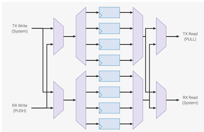
Another example is a UART: because the TX/CTS and RX/RTS parts of a UART are asynchronous, they are implemented on two separate state machines. It would be wasteful to leave half of each state machine's FIFO resources idle. The ability to join the two halves into just a TX FIFO for the TX/CTS state machine, or just an RX FIFO in the case of the RX/RTS state machine, allows full utilisation. A UART equipped with an 8-deep FIFO can be left alone for twice as long between interrupts as one with only a 4-deep FIFO.
When one FIFO is increased in size (from 4 to 8), the other FIFO on that state machine is reduced to zero. For example, if joining to TX, the RX FIFO is unavailable, and any PUSH instruction will stall. The RX FIFO will appear both RXFULL and RXEMPTY in the FSTAT register. The converse is true if joining to RX: the TX FIFO is unavailable, and the TXFULL and TXEMPTY bits for this state machine will both be set in FSTAT . Setting both FJOIN_RX and FJOIN_TX makes both FIFOs unavailable.
8 FIFO entries is sufficient for 1 word per clock through the RP2350 system DMA, provided the DMA is not slowed by contention with other masters.
⚠ CAUTION
Changing FJOIN discards any data present in the state machine's FIFOs. If this data is irreplaceable, it must be drained beforehand.
11.5.4. Autopush and Autopull
With each OUT instruction, the OSR gradually empties, as data is shifted out. Once empty, it must be refilled: for example, a PULL transfers one word of data from the TX FIFO to the OSR. Similarly, the ISR must be emptied once full. One approach to this is a loop which performs a PULL after an appropriate amount of data has been shifted:
1 .program manual_pull
2 .side_set 1 opt
3
4 .wrap_target
5     set x, 2                ; X = bit count - 2
6     pull                    side 1 [1] ; Stall here if no TX data
7 bitloop:
8     out pins, 1             side 0 [1] ; Shift out data bit and toggle clock low
9     jmp x-- bitloop         side 1 [1] ; Loop runs 3 times
10    out pins, 1             side 0      ; Shift out last bit before reloading X
11 .wrap
This program shifts out 4 bits from each FIFO word, with an accompanying bit clock, at a constant rate of 1 bit per 4 cycles. When the TX FIFO is empty, it stalls with the clock high (noting that side-set still takes place on cycles where the
instruction stalls). Figure 49 shows how a state machine would execute this program.
Figure 49. Execution of
manual_pull
program.
X
is used as a loop counter. On each iteration, one data bit is shifted out, and the clock is asserted low, then high. A delay cycle on each instruction brings the total up to four cycles per iteration. After the third loop, a fourth bit is shifted out, and the state machine immediately returns to the start of the program to reload the loop counter and pull fresh data, while maintaining the 4 cycles/bit cadence.
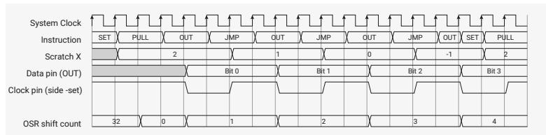
| System Clock | Instruction | Scratch X | Data pin (OUT) | Clock pin (side-set) | OSR shift count |
|---|---|---|---|---|---|
| 1 | SET | 32 | |||
| 2 | PULL | 32 | |||
| 3 | OUT | 2 | Bit 0 | Low | 31 |
| 4 | JMP | High | 30 | ||
| 5 | PULL | 30 | |||
| 6 | OUT | 1 | Bit 1 | Low | 29 |
| 7 | JMP | High | 28 | ||
| 8 | PULL | 28 | |||
| 9 | OUT | 0 | Bit 2 | Low | 27 |
| 10 | JMP | High | 26 | ||
| 11 | PULL | 26 | |||
| 12 | OUT | -1 | Bit 3 | Low | 25 |
| 13 | JMP | High | 24 | ||
| 14 | PULL | 24 | |||
| 15 | OUT | 2 | Bit 0 | Low | 23 |
| 16 | JMP | High | 22 |
This program has some limitations:
- It occupies 5 instruction slots, but only 2 of these are immediately useful (
out pins, 1 set 0and... set 1), for outputting serial data and a clock. - Throughput is limited to system clock over 4, due to the extra cycles required to pull in new data, and reload the loop counter.
This is a common type of problem for PIO, so each state machine has some extra hardware to handle it. State machines keep track of the total shift count
OUT
of the OSR and
IN
to the ISR, and trigger certain actions once these counters reach a programmable threshold.
- On an
OUTinstruction which reaches or exceeds the pull threshold, the state machine can simultaneously refill the OSR from the TX FIFO, if data is available. - On an
INinstruction which reaches or exceeds the push threshold, the state machine can write the shift result directly to the RX FIFO, and clear the ISR.
The
manual_pull
example can be rewritten to take advantage of automatic pull (autopull):
1 .program autopull
2 .side_set 1
3
4 .wrap_target
5     out pins, 1    side 0    [1]
6     nop           side 1    [1]
7 .wrap
This is shorter and simpler than the original, and can run
twice
as fast, if the delay cycles are removed, since the hardware refills the OSR "for free". Note that the program does not determine the total number of bits to be shifted before the next pull; the hardware automatically pulls once the programmable threshold,
SHIFCTRL_PULL_THRESH
, is reached, so the same program could also shift out e.g. 16 or 32 bits from each FIFO word.
Finally, note that the above program is not
exactly
the same as the original, since it stalls with the clock output low, rather than high. We can change the location of the stall, using the
PULL IFEMPTY
instruction, which uses the same configurable threshold as autopull:
1 .program somewhat_manual_pull
2 .side_set 1
3
4 .wrap_target
5     out pins, 1    side 0    [1]
6     pull ifempty  side 1    [1]
7 .wrap
Below is a complete example (PIO program, plus a C program to load and run it) which illustrates autopull and autopush both enabled on the same state machine. It programs state machine 0 to loopback data from the TX FIFO to the RX FIFO, with a throughput of one word per two clocks. It also demonstrates how the state machine will stall if it tries to
OUT
when both the OSR and TX FIFO are empty.
1 .program auto_push_pull
2
3 .wrap_target
4     out x, 32
5     in x, 32
6 .wrap
1 #include "tb.h" // TODO this is built against existing sw tree, so that we get printf etc
2
3 #include "platform.h"
4 #include "pio_regs.h"
5 #include "system.h"
6 #include "hardware.h"
7
8 #include "auto_push_pull.pio.h"
9
10 int main()
11 {
12     tb_init();
13
14     // Load program and configure state machine 0 for autopush/pull with
15     // threshold of 32, and wrapping on program boundary. A threshold of 32 is
16     // encoded by a register value of 00000.
17     for (int i = 0; i < count_of(auto_push_pull_program); ++i)
18         mm_pio->instr_mem[i] = auto_push_pull_program[i];
19     mm_pio->sm[0].shiftctrl =
20         (1u << PIO_SM0_SHIFTCTRL_AUTOPUSH_LSB) |
21         (1u << PIO_SM0_SHIFTCTRL_AUTOPULL_LSB) |
22         (0u << PIO_SM0_SHIFTCTRL_PUSH_THRESH_LSB) |
23         (0u << PIO_SM0_SHIFTCTRL_PULL_THRESH_LSB);
24     mm_pio->sm[0].execctrl =
25         (auto_push_pull_wrap_target << PIO_SM0_EXECCTRL_WRAP_BOTTOM_LSB) |
26         (auto_push_pull_wrap << PIO_SM0_EXECCTRL_WRAP_TOP_LSB);
27
28     // Start state machine 0
29     hw_set_bits(&mm_pio->ctrl, 1u << (PIO_CTRL_SM_ENABLE_LSB + 0));
30
31     // Push data into TX FIFO, and pop from RX FIFO
32     for (int i = 0; i < 5; ++i)
33         mm_pio->txf[0] = i;
34     for (int i = 0; i < 5; ++i)
35         printf("%d\n", mm_pio->rx[0]);
36
37     return 0;
38 }
Figure 50 shows how the state machine executes the example program. Initially the OSR is empty, so the state machine stalls on the first OUT instruction. Once data is available in the TX FIFO, the state machine transfers this into the OSR. On the next cycle, the OUT can execute using the data in the OSR (in this case, transferring this data to the X scratch register), and the state machine simultaneously refills the OSR with fresh data from the FIFO. Since every IN instruction immediately fills the ISR, the ISR remains empty, and IN transfers data directly from scratch X to the RX FIFO.
Figure 50. Execution of
auto_push_pull
program. The state machine stalls on an
OUT
until data has travelled through the
TX FIFO
into the
OSR
. Subsequently, the
OSR
is refilled simultaneously with each
OUT
operation (due to bit count of 32), and
IN
data bypasses the
ISR
and goes straight to the
RX FIFO
. The state machine stalls again when the
FIFO
has drained, and the
OSR
is once again empty.
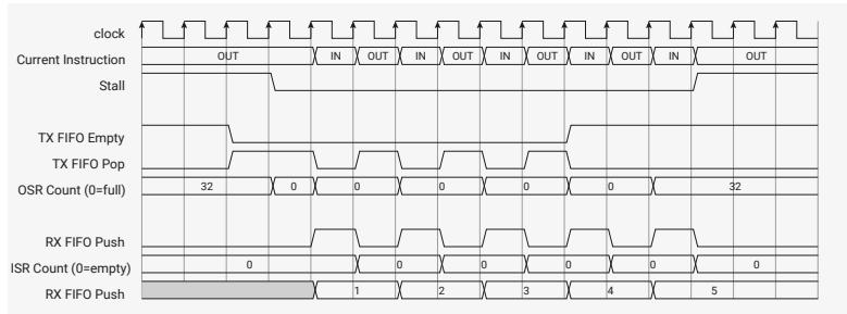
To trigger automatic push or pull at the correct time, the state machine tracks the total shift count of the
ISR
and
OSR
, using a pair of saturating 6-bit counters.
- • At reset, or upon
CTRL_SM_RESTARTassertion,ISRshift counter is set to 0 (nothing shifted in), andOSRto 32 (nothing left to be shifted out) - • An
OUTinstruction increases theOSRshift counter byBit count - • An
INinstruction increases theISRshift counter byBit count - • A
PULLinstruction or autopull clears theOSRcounter to 0 - • A
PUSHinstruction or autopush clears theISRcounter to 0 - • A
MOV OSR, xorMOV ISR, xclears theOSRorISRshift counter to 0, respectively - • A
OUT ISR, ninstruction sets theISRshift counter ton
On any
OUT
or
IN
instruction, the state machine compares the shift counters to the values of
SHIFTCTRL_PULL_THRESH
and
SHIFTCTRL_PUSH_THRESH
to decide whether action is required. Autopull and autopush are individually enabled by the
SHIFTCTRL_AUTOPULL
and
SHIFTCTRL_AUTOPUSH
fields.
11.5.4.1. Autopush details
Pseudocode for an
IN
with autopush enabled:
1 isr = shift_in(isr, input())
2 isr count = saturate(isr count + in count)
3
4 if rx count >= threshold:
5     if rx fifo is full:
6         stall
7     else:
8         push(isr)
9         isr = 0
10        isr count = 0
The hardware performs the above steps in a single machine clock cycle, unless there is a stall.
Threshold is configurable from 1 to 32.
! IMPORTANTAutopush must not be enabled when
SHIFTCTRL_FJOIN_RX_PUT
or
SHIFTCTRL_FJOIN_RX_GET
is set. Its operation in this state is undefined.
On non- OUT cycles, the hardware performs the equivalent of the following pseudocode:
1 if MOV or PULL:
2     osr count = 0
3
4 if osr count >= threshold:
5     if tx fifo not empty:
6         osr = pull()
7         osr count = 0
An autopull can therefore occur at any point between two OUT s, depending on when the data arrives in the FIFO.
On OUT cycles, the sequence is a little different:
1 if osr count >= threshold:
2     if tx fifo not empty:
3         osr = pull()
4         osr count = 0
5     stall
6 else:
7     output(osr)
8     osr = shift(osr, out count)
9     osr count = saturate(osr count + out count)
10
11 if osr count >= threshold:
12     if tx fifo not empty:
13         osr = pull()
14         osr count = 0
The hardware is capable of refilling the OSR simultaneously with shifting out the last of the shift data, as these two operations can proceed in parallel. However, it cannot fill an empty OSR and OUT it on the same cycle, due to the long logic path this would create.
The refill is somewhat asynchronous to your program, but an OUT behaves as a data fence, and the state machine will never OUT data which you didn't write into the FIFO.
Note that a MOV from the OSR is undefined whilst autopull is enabled; you will read either any residual data that has not been shifted out, or a fresh word from the FIFO, depending on a race against system DMA. Likewise, a MOV to the OSR may overwrite data which has just been autopulled. However, data which you MOV into the OSR will never be overwritten, since MOV updates the shift counter.
If you do need to read the OSR contents, you should perform an explicit PULL of some kind. The nondeterminism described above is the cost of the hardware managing pulls automatically. When autopull is enabled, the behaviour of PULL is altered: it becomes a no-op if the OSR is full. This is to avoid a race condition against the system DMA. It behaves as a fence: either an autopull has already taken place, in which case the PULL has no effect, or the program will stall on the PULL until data becomes available in the FIFO.
PULL does not require similar behaviour, because autopush does not have the same nondeterminism.
11.5.5. Clock Dividers
PIO runs off the system clock, but this is too fast for many interfaces, and the number of De lay cycles which can be inserted is limited. Some devices, such as UART, require the signalling rate to be precisely controlled and varied, and ideally multiple state machines can be varied independently while running identical programs. Each state machine is equipped with a clock divider, for this purpose.
Rather than slowing the system clock itself, the clock divider redefines how many system clock periods are considered to be "one cycle", for execution purposes. It does this by generating a clock enable signal, which can pause and resume execution on a per-system-clock-cycle basis. The clock divider generates clock enable pulses at regular intervals, so that the state machine runs at some steady pace, potentially much slower than the system clock.
Implementing the clock dividers in this way allows interfacing between the state machines and the system to be simpler, lower-latency, and with a smaller footprint. The state machine is completely idle on cycles where clock enable is low, though the system can still access the state machine's FIFOs and change its configuration.
The clock dividers are 16-bit integer, 8-bit fractional, with first-order delta-sigma for the fractional divider. The clock divisor can vary between 1 and 65536, in increments of \( 1/256 \) .
If the clock divisor is set to 1, the state machine runs on every cycle, i.e. full speed:
Figure 51. State machine operation with a clock divisor of 1. Once the state machine is enabled via the CTRL register, its clock enable is asserted on every cycle.
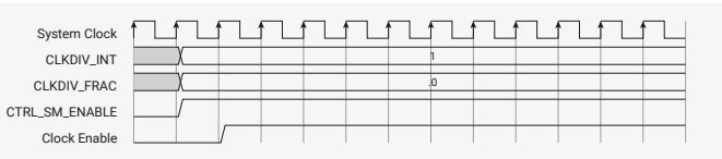
The diagram shows a series of system clock cycles. The CLKDIV_INT register is set to 1 and CLKDIV_FRAC is 0. The CTRL_SM_ENABLE signal is asserted at the start. The resulting Clock Enable signal is a continuous high pulse, indicating the state machine runs at full speed.
In general, an integer clock divisor of \( n \) will cause the state machine to run 1 cycle in every \( n \) , giving an effective clock speed of \( f_{sys} / n \) .
Figure 52. Integer clock divisors yield a periodic clock enable. The clock divider repeatedly counts down from \( n \) , and emits an enable pulse when it reaches 1.
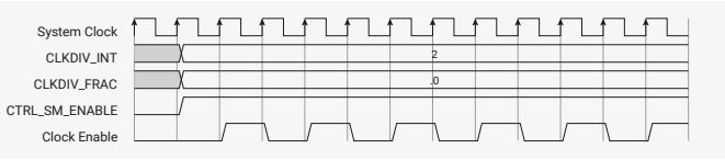
The diagram shows the system clock and the state machine's clock enable signal for an integer divisor of 2. The CLKDIV_INT register is set to 2 and CLKDIV_FRAC is 0. The Clock Enable signal is a periodic pulse that is high for one system clock cycle and low for the next, resulting in the state machine running at half the system clock speed.
Fractional division will maintain a steady state division rate of \( n + f / 256 \) , where \( n \) and \( f \) are the integer and fractional fields of this state machine's CLKDIV register. It does this by selectively extending some division periods from \( n \) cycles to \( n + 1 \) .
Figure 53. Fractional clock division with an average divisor of 2.5. The clock divider maintains a running total of the fractional value from each division period, and every time this value wraps through 1, the integer divisor is increased by one for the next division period.

The diagram shows the system clock and the state machine's clock enable signal for a fractional divisor. The CLKDIV_INT register is set to 2 and CLKDIV_FRAC is 5 (representing 0.01953125). The Clock Enable signal is a periodic pulse that is high for 2 or 3 system clock cycles, maintaining an average division rate of 2.5.
For small \( n \) , the jitter introduced by a fractional divider may be unacceptable. However, for larger values, this effect is much less apparent.
NOTE
For fast asynchronous serial, it is recommended to use even divisions or multiples of 1 Mbaud where possible, rather than the traditional multiples of 300, to avoid unnecessary jitter.
11.5.6. GPIO mapping
Internally, PIO has a 32-bit register for the output levels of each GPIO it can drive, and another register for the output enables (Hi/Lo-Z). On every system clock cycle, each state machine can write to some or all of the GPIOs in each of these registers.
Figure 54. The state machine has two independent output channels, one shared by OUT/SET, and another used by side-set (which can happen at any time). Three independent mappings (first GPIO, number of GPIOs OUT, SET and side-set are directed to. Input data is rotated according to which GPIO is mapped to the LSB of the IN data.
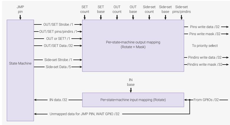
The write data and write masks for the output level and output enable registers come from the following sources:
- • An OUT instruction writes to up to 32 bits. Depending on the instruction's Destination field, this is applied to either pins or pindirs. The least-significant bit of OUT data is mapped to PINCTRL_OUT_BASE , and this mapping continues for PINCTRL_OUT_COUNT bits, wrapping after GPIO31.
- • A SET instruction writes up to 5 bits. Depending on the instruction's Destination field, this is applied to either pins or pindirs. The least-significant bit of SET data is mapped to PINCTRL_SET_BASE , and this mapping continues for PINCTRL_SET_COUNT bits, wrapping after GPIO31.
- • A side-set operation writes up to 5 bits. Depending on the register field EXECCTRL_SIDE_PINDIR , this is applied to either pins or pindirs. The least-significant bit of side-set data is mapped to PINCTRL_SIDESET_BASE , continuing for PINCTRL_SIDESET_COUNT pins, minus one if EXECCTRL_SIDE_EN is set.
Each OUT/SET/side-set operation writes to a contiguous range of pins, but each of these ranges is independently sized and positioned in the 32-bit GPIO space. This is sufficiently flexible for many applications. For example, if one state machine is implementing some interface such as an SPI on a group of pins, another state machine can run the same program, mapped to a different group of pins, and provide a second SPI interface.
On any given clock cycle, the state machine may perform an OUT or a SET , and may simultaneously perform a side-set. The pin mapping logic generates a 32-bit write mask and write data bus for the output level and output enable registers, based on this request, and the pin mapping configuration.
If a side-set overlaps with an OUT/SET performed by that state machine on the same cycle, the side-set takes precedence in the overlapping region.
11.5.6.1. Output priority
Figure 55. Per-GPIO priority select of write masks from each state machine. Each GPIO considers level and direction writes from each of the four state machines, and applies the value from the highest-numbered state machine.
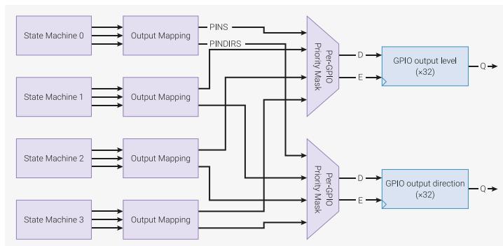
Each state machine may assert an OUT/SET and a side-set through its pin mapping hardware on each cycle. This generates 32 bits of write data and write mask for the GPIO output level and output enable registers, from each state machine.
For each GPIO, PIO collates the writes from all four state machines, and applies the write from the highest-numbered
state machine. This occurs separately for output levels and output values – it is possible for a state machine to change both the level and direction of the same pin on the same cycle (e.g. via simultaneous SET and side-set), or for one state machine to change a GPIO's direction while another changes that GPIO's level. If no state machine asserts a write to a GPIO's level or direction, the value does not change.
11.5.6.2. Input mapping
The data observed by IN instructions is mapped such that the LSB is the GPIO selected by PINCTRL_IN_BASE , and successively more-significant bits come from successively higher-numbered GPIOs, wrapping after 31.
In other words, the IN bus is a right-rotate of the GPIO input values, by PINCTRL_IN_BASE . If fewer than 32 GPIOs are present, the PIO input is padded with zeroes up to 32 bits.
Some instructions, such as WAIT GPIO , use an absolute GPIO number, rather than an index into the IN data bus. In this case, the right-rotate is not applied.
11.5.6.3. Input synchronisers
To protect PIO from metastabilities, each GPIO input is equipped with a standard 2-flipflop synchroniser. This adds two cycles of latency to input sampling, but the benefit is that state machines can perform an IN PINS at any point, and will see only a clean high or low level, not some intermediate value that could disturb the state machine circuitry. This is absolutely necessary for asynchronous interfaces such as UART RX.
It is possible to bypass these synchronisers, on a per-GPIO basis. This reduces input latency, but it is then up to the user to guarantee that the state machine does not sample its inputs at inappropriate times. Generally this is only possible for synchronous interfaces such as SPI. Synchronisers are bypassed by setting the corresponding bit in INPUT_SYNC_BYPASS .
 WARNING
Sampling a metastable input can lead to unpredictable state machine behaviour. This should be avoided.
11.5.7. Forced and EXEC'd instructions
Besides the instruction memory, state machines can execute instructions from 3 other sources:
- • MOV EXEC which executes an instruction from some register Source
- • OUT EXEC which executes data shifted out from the OSR
- • The SMx_INSTR control registers, to which the system can write instructions for immediate execution
1 .program exec_example
2
3 hang:
4     jmp hang
5 execute:
6     out exec, 32
7     jmp execute
8
9 .program instructions_to_push
10
11     out x, 32
12     in x, 32
13     push
1  #include "tb.h" // TODO this is built against existing sw tree, so that we get printf etc
2
3  #include "platform.h"
4  #include "pio_regs.h"
5  #include "system.h"
6  #include "hardware.h"
7
8  #include "exec_example.pio.h"
9
10 int main()
11 {
12     tb_init();
13
14     for (int i = 0; i < count_of(exec_example_program); ++i)
15         mm_pio->instr_mem[i] = exec_example_program[i];
16
17     // Enable autopull, threshold of 32
18     mm_pio->sm[0].shiftctrl = (1u << PIO_SM0_SHIFTCTRL_AUTOPULL_LSB);
19
20     // Start state machine 0 -- will sit in "hang" loop
21     hw_set_bits(&mm_pio->ctrl, 1u << (PIO_CTRL_SM_ENABLE_LSB + 0));
22
23     // Force a jump to program location 1
24     mm_pio->sm[0].instr = 0x0000 | 0x1; // jmp execute
25
26     // Feed a mixture of instructions and data into FIFO
27     mm_pio->txf[0] = instructions_to_push_program[0]; // out x, 32
28     mm_pio->txf[0] = 12345678; // data to be OUTed
29     mm_pio->txf[0] = instructions_to_push_program[1]; // in x, 32
30     mm_pio->txf[0] = instructions_to_push_program[2]; // push
31
32     // The program pushed into TX FIFO will return some data in RX FIFO
33     while (mm_pio->fstat & (1u << PIO_FSTAT_RXEMPTY_LSB))
34         ;
35
36     printf("%d\n", mm_pio->rx[0]);
37
38     return 0;
39 }
Here we load an example program into the state machine, which does two things:
- • Enters an infinite loop
- • Enters a loop which repeatedly pulls 32 bits of data from the TX FIFO, and executes the lower 16 bits as an instruction
The C program sets the state machine running, at which point it enters the hang loop. While the state machine is still running, the C program forces in a jmp instruction, which causes the state machine to break out of the loop.
When an instruction is written to the INSTR register, the state machine immediately decodes and executes that instruction, rather than the instruction it would have fetched from the PIO's instruction memory. The program counter does not advance, so on the next cycle (assuming the instruction forced into the INSTR interface did not stall) the state machine continues to execute its current program from the point where it left off, unless the written instruction itself manipulated PC .
Delay cycles are ignored on instructions written to the INSTR register, and execute immediately, ignoring the state machine clock divider. This interface is provided for performing initial setup and effecting control flow changes, so it executes instructions in a timely manner, no matter how the state machine is configured.
Instructions written to the INSTR register are permitted to stall, in which case the state machine will latch this instruction internally until it completes. This is signified by the EXECCTRL_EXEC_STALLED flag. This can be cleared by restarting the state
machine, or writing a
NOP
to
INSTR
.
In the second phase of the example state machine program, the
OUT EXEC
instruction is used. The
OUT
itself occupies one execution cycle, and the instruction which the
OUT
executes is on the next execution cycle. Note that one of the instructions we execute is also an
OUT
— the state machine is only capable of executing one
OUT
instruction on any given cycle.
OUT EXEC
works by writing the
OUT
shift data to an internal instruction latch. On the next cycle, the state machine remembers it must execute from this latch rather than the instruction memory, and also knows to not advance
PC
on this second cycle.
This program will print "12345678" when run.
 CAUTION
If an instruction written to
INSTR
stalls, it is stored in the same instruction latch used by
OUT EXEC
and
MOV EXEC
, and will overwrite an in-progress instruction there. If
EXEC
instructions are used, instructions written to
INSTR
must not stall.
11.6. Examples
These examples illustrate some of PIO's hardware features, by implementing common I/O interfaces.
 TIP
TIP
Raspberry Pi Pico-series C/C++ SDK has a comprehensive PIO chapter that begins with writing and building your first PIO application. Later chapters walk through some programs line-by-line. Finally, it covers broader topics such as using PIO with DMA, and how PIO can integrate into your software.
11.6.1. Duplex SPI
Figure 56. In SPI, a host and device exchange data over a bidirectional pair of serial data lines, synchronous with a clock (SCK). Two flags, CPOL and CPHA, specify the clock's behaviour. CPOL is the idle state of the clock: 0 for low, 1 for high. The clock pulses a number of times, transferring one bit in each direction per pulse, but always returns to its idle state. CPHA determines on which edge of the clock data is captured: 0 for leading edge, and 1 for trailing edge. The arrows in the figure show the clock edge where data is captured by both the host and device.
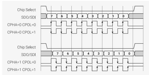
SPI is a common serial interface with a twisty history. The following program implements full-duplex (i.e. transferring data in both directions simultaneously) SPI, with a CPHA parameter of 0.
Pico Examples: https://github.com/raspberrypi/pico-examples/blob/master/pio/spi/spi.pio Lines 14 - 32
14 .program spi_cpha0
15 .side_set 1
16
17 ; Pin assignments:
18 ; - SCK is side-set pin 0
19 ; - MOSI is OUT pin 0
20 ; - MISO is IN pin 0
21 ;
22 ; Autopush and autopull must be enabled, and the serial frame size is set by
23 ; configuring the push/pull threshold. Shift left/right is fine, but you must
24 ; justify the data yourself. This is done most conveniently for frame sizes of
25 ; 8 or 16 bits by using the narrow store replication and narrow load byte
26 ; picking behaviour of RP2040's IO fabric.
27
28 ; Clock phase = 0: data is captured on the leading edge of each SCK pulse, and
29 ; transitions on the trailing edge, or some time before the first leading edge.
30
31     out pins, 1 side 0 [1] ; Stall here on empty (sideset proceeds even if
32     in pins, 1 side 1 [1] ; instruction stalls, so we stall with SCK low)
This code uses autopush and autopull to continuously stream data from the FIFOs. The entire program runs once for every bit that is transferred, and then loops. The state machine tracks how many bits have been shifted in/out, and automatically pushes/pulls the FIFOs at the correct point. A similar program handles the CPHA=1 case:
Pico Examples: https://github.com/raspberrypi/pico-examples/blob/master/pio/spi/spi.pio Lines 34 - 42
34 .program spi_cpha1
35 .side_set 1
36
37 ; Clock phase = 1: data transitions on the leading edge of each SCK pulse, and
38 ; is captured on the trailing edge.
39
40     out x, 1 side 0 ; Stall here on empty (keep SCK deasserted)
41     mov pins, x side 1 [1] ; Output data, assert SCK (mov pins uses OUT mapping)
42     in pins, 1 side 0 ; Input data, deassert SCK
29     if (rx_remain && !pio_sm_is_rx_fifo_empty(spi->pio, spi->sm)) {
30         (void) *rxfifo;
31         --rx_remain;
32     }
33 }
34 }
Putting this all together, this complete C program will loop back some data through a PIO SPI at 1 MHz, with all four CPOL/CPHA combinations:
Pico Examples: https://github.com/raspberrypi/pico-examples/blob/master/pio/spi/spi_loopback.c
1  /**
2   * Copyright (c) 2020 Raspberry Pi (Trading) Ltd.
3   *
4   * SPDX-License-Identifier: BSD-3-Clause
5   */
6
7  #include <stdlib.h>
8  #include <stdio.h>
9
10 #include "pico/stdlib.h"
11 #include "pio_spi.h"
12
13 // This program instantiates a PIO SPI with each of the four possible
14 // CPOL/CPHA combinations, with the serial input and output pin mapped to the
15 // same GPIO. Any data written into the state machine's TX FIFO should then be
16 // serialised, deserialised, and reappear in the state machine's RX FIFO.
17
18 #define PIN_SCK 18
19 #define PIN_MOSI 16
20 #define PIN_MISO 16 // same as MOSI, so we get loopback
21
22 #define BUF_SIZE 20
23
24 void test(const pio_spi_inst_t *spi) {
25     static uint8_t txbuf[BUF_SIZE];
26     static uint8_t rxbuf[BUF_SIZE];
27     printf("TX:");
28     for (int i = 0; i < BUF_SIZE; ++i) {
29         txbuf[i] = rand() >> 16;
30         rxbuf[i] = 0;
31         printf(" %02x", (int) txbuf[i]);
32     }
33     printf("\n");
34
35     pio_spi_write8_read8_blocking(spi, txbuf, rxbuf, BUF_SIZE);
36
37     printf("RX:");
38     bool mismatch = false;
39     for (int i = 0; i < BUF_SIZE; ++i) {
40         printf(" %02x", (int) rxbuf[i]);
41         mismatch = mismatch || rxbuf[i] != txbuf[i];
42     }
43     if (mismatch)
44         printf("\nNope\n");
45     else
46         printf("\nOK\n");
47 }
48
49 int main() {
50     stdio_init_all();
51
52     pio_spi_inst_t spi = {
53         .pio = pio0,
54         .sm = 0
55     };
56     float clkdiv = 31.25f; // 1 MHz @ 125 clk_sys
57     uint cpha0_prog_offs = pio_add_program(spi.pio, &spi_cpha0_program);
58     uint cpha1_prog_offs = pio_add_program(spi.pio, &spi_cpha1_program);
59
60     for (int cpha = 0; cpha <= 1; ++cpha) {
61         for (int cpol = 0; cpol <= 1; ++cpol) {
62             printf("CPHA = %d, CPOL = %d\n", cpha, cpol);
63             pio_spi_init(spi.pio, spi.sm,
64                         cpha ? cpha1_prog_offs : cpha0_prog_offs,
65                         8, // 8 bits per SPI frame
66                         clkdiv,
67                         cpha,
68                         cpol,
69                         PIN_SCK,
70                         PIN_MOSI,
71                         PIN_MISO
72             );
73             test(&spi);
74             sleep_ms(10);
75         }
76     }
77 }
11.6.2. WS2812 LEDs
WS2812 LEDs are driven by a proprietary pulse-width serial format, with a wide positive pulse representing a "1" bit, and narrow positive pulse a "0". Each LED has a serial input and a serial output; LEDs are connected in a chain, with each serial input connected to the previous LED's serial output.
Figure 57. WS2812 line format. Wide positive pulse for 1, narrow positive pulse for 0, very long negative pulse for latch enable

The diagram illustrates the WS2812 line format. It shows a sequence of pulses: a wide positive pulse for '1', a narrow positive pulse for '0', and a very long negative pulse for 'Latch'. The diagram is labeled 'Symbol' and 'Output'.
LEDs consume 24 bits of pixel data, then pass any additional input data on to their output. In this way a single serial burst can individually program the colour of each LED in a chain. A long negative pulse latches the pixel data into the LEDs.
Pico Examples: https://github.com/raspberrypi/pico-examples/blob/master/pio/ws2812/ws2812.pio Lines 8 - 31
8 .program ws2812
9 .side_set 1
10
11 ; The following constants are selected for broad compatibility with WS2812,
12 ; WS2812B, and SK6812 LEDs. Other constants may support higher bandwidths for
13 ; specific LEDs, such as (7,10,8) for WS2812B LEDs.
14
15 .define public T1 3
16 .define public T2 3
17 .define public T3 4
18
19 .lang_opt python sideset_init = pico.PIO.OUT_HIGH
20 .lang_opt python out_init     = pico.PIO.OUT_HIGH
21 .lang_opt python out_shiftdir = 1
22
23 .wrap_target
24 bitloop:
25     out x, 1          side 0 [T3 - 1] ; Side-set still takes place when instruction stalls
26     jmp !x do_zero side 1 [T1 - 1] ; Branch on the bit we shifted out. Positive pulse
27 do_one:
28     jmp bitloop      side 1 [T2 - 1] ; Continue driving high, for a long pulse
29 do_zero:
30     nop              side 0 [T2 - 1] ; Or drive low, for a short pulse
31 .wrap
This program shifts bits from the OSR into X, and produces a wide or narrow pulse on side-set pin 0, based on the value of each data bit. Autopull must be configured, with a threshold of 24. Software can then write 24-bit pixel values into the FIFO, and these will be serialised to a chain of WS2812 LEDs. The
.pio
file contains a C helper function to set this up:
Pico Examples: https://github.com/raspberrypi/pico-examples/blob/master/pio/ws2812/ws2812.pio Lines 36 - 52
36 static inline void ws2812_program_init(PIO pio, uint sm, uint offset, uint pin, float freq,
    bool rgbw) {
37
38     pio_gpio_init(pio, pin);
39     pio_sm_set_consecutive_pindirs(pio, sm, pin, 1, true);
40
41     pio_sm_config c = ws2812_program_get_default_config(offset);
42     sm_config_set_sideset_pins(&c, pin);
43     sm_config_set_out_shift(&c, false, true, rgbw ? 32 : 24);
44     sm_config_set_fifo_join(&c, PIO_FIFO_JOIN_TX);
45
46     int cycles_per_bit = ws2812_T1 + ws2812_T2 + ws2812_T3;
47     float div = clock_get_hz(clk_sys) / (freq * cycles_per_bit);
48     sm_config_set_clkdiv(&c, div);
49
50     pio_sm_init(pio, sm, offset, &c);
51     pio_sm_set_enabled(pio, sm, true);
52 }
Because the shift is MSB-first, and our pixels aren't a power of two size (so we can't rely on the narrow write replication behaviour on RP2350 to fan out the bits for us), we need to preshift the values written to the TX FIFO.
Pico Examples: https://github.com/raspberrypi/pico-examples/blob/master/pio/ws2812/ws2812.c Lines 43 - 45
43 static inline void put_pixel(PIO pio, uint sm, uint32_t pixel_grb) {
44     pio_sm_put_blocking(pio, sm, pixel_grb << 8u);
45 }
To DMA the pixels, we could instead set the autopull threshold to 8 bits, set the DMA transfer size to 8 bits, and write a byte at a time into the FIFO. Each pixel would be 3 one-byte transfers. Because of how the bus fabric and DMA on RP2350 work, each byte the DMA transfers will appear replicated four times when written to a 32-bit IO register, so effectively your data is at both ends of the shift register, and you can shift in either direction without worry.
TIP
The WS2812 example is the subject of a tutorial in the
Raspberry Pi Pico-series C/C++ SDK
document, in the PIO chapter. The tutorial dissects the
ws2812
program line by line, traces through how the program executes, and shows wave diagrams of the GPIO output at every point in the program.
11.6.3. UART TX
Figure 58. UART serial format. The line is high when idle. The transmitter pulls the line down for one bit period to signify the start of a serial frame (the "start bit"), and a small, fixed number of data bits follows. The line returns to the idle state for at least one bit period (the "stop bit") before the next serial frame can begin.

This program implements the transmit component of a universal asynchronous receive/transmit (UART) serial peripheral. Perhaps it would be more correct to refer to this as a UAT.
Pico Examples: https://github.com/raspberrypi/pico-examples/blob/master/pio/uart_tx/uart_tx.pio Lines 8 - 18
8 .program uart_tx
9 .side_set 1 opt
10
11 ; An 8n1 UART transmit program.
12 ; OUT pin 0 and side-set pin 0 are both mapped to UART TX pin.
13
14     pull            side 1 [7] ; Assert stop bit, or stall with line in idle state
15     set x, 7        side 0 [7] ; Preload bit counter, assert start bit for 8 clocks
16 bitloop:                ; This loop will run 8 times (8n1 UART)
17     out pins, 1         ; Shift 1 bit from QSR to the first OUT pin
18     jmp x-- bitloop    [6] ; Each loop iteration is 8 cycles.
As written, it will:
- 1. Stall with the pin driven high until data appears (noting that side-set takes effect even when the state machine is stalled)
- 2. Assert a start bit, for 8 SM execution cycles
- 3. Shift out 8 data bits, each lasting for 8 cycles
- 4. Return to the idle line state for at least 8 cycles before asserting the next start bit
If the state machine's clock divider is configured to run at 8 times the desired baud rate, this program will transmit well-formed UART serial frames, whenever data is pushed to the TX FIFO either by software or the system DMA. To extend the program to cover different frame sizes (different numbers of data bits), the
set x, 7
could be replaced with
mov x, y
, so that the
y
scratch register becomes a per-SM configuration register for UART frame size.
The
.pio
file in the SDK also contains this function, for configuring the pins and the state machine, once the program has been loaded into the PIO instruction memory:
Pico Examples: https://github.com/raspberrypi/pico-examples/blob/master/pio/uart_tx/uart_tx.pio Lines 24 - 51
24 static inline void uart_tx_program_init(PIO pio, uint sm, uint offset, uint pin_tx, uint
    baud) {
25     // Tell PIO to initially drive output-high on the selected pin, then map PIO
26     // onto that pin with the IO muxes.
27     pio_sm_set_pins_with_mask64(pio, sm, 1ull << pin_tx, 1ull << pin_tx);
28     pio_sm_set_pindirs_with_mask64(pio, sm, 1ull << pin_tx, 1ull << pin_tx);
29     pio_gpio_init(pio, pin_tx);
30
31     pio_sm_config c = uart_tx_program_get_default_config(offset);
32 33 // OUT shifts to right, no autopull 34 sm_config_set_out_shift(&c, true, false, 32); 35 36 // We are mapping both OUT and side-set to the same pin, because sometimes 37 // we need to assert user data onto the pin (with OUT) and sometimes 38 // assert constant values (start/stop bit) 39 sm_config_set_out_pins(&c, pin_tx, 1); 40 sm_config_set_sideset_pins(&c, pin_tx); 41 42 // We only need TX, so get an 8-deep FIFO! 43 sm_config_set_fifo_join(&c, PIO_FIFO_JOIN_TX); 44 45 // SM transmits 1 bit per 8 execution cycles. 46 float div = (float)clock_get_hz(clk_sys) / (8 * baud); 47 sm_config_set_clkdiv(&c, div); 48 49 pio_sm_init(pio, sm, offset, &c); 50 pio_sm_set_enabled(pio, sm, true); 51 }
The state machine is configured to shift right in
out
instructions, because UARTs typically send data LSB-first. Once configured, the state machine will print any characters pushed to the TX FIFO.
Pico Examples: https://github.com/raspberrypi/pico-examples/blob/master/pio/uart_tx/uart_tx.pio Lines 53 - 55
53 static inline void uart_tx_program_putc(PIO pio, uint sm, char c) {
54     pio_sm_put_blocking(pio, sm, (uint32_t)c);
55 }
Pico Examples: https://github.com/raspberrypi/pico-examples/blob/master/pio/uart_tx/uart_tx.pio Lines 57 - 60
57 static inline void uart_tx_program_puts(PIO pio, uint sm, const char *s) {
58     while (*s)
59         uart_tx_program_putc(pio, sm, *s++);
60 }
The example program in the SDK will configure one PIO state machine as a UART TX peripheral, and use it to print a message on GPIO 0 at 115200 baud once per second.
Pico Examples: https://github.com/raspberrypi/pico-examples/blob/master/pio/uart_tx/uart_tx.c
1 /**
2  * Copyright (c) 2020 Raspberry Pi (Trading) Ltd.
3  *
4  * SPDX-License-Identifier: BSD-3-Clause
5  */
6
7 #include "pico/stdlib.h"
8 #include "hardware/pio.h"
9 #include "uart_tx.pio.h"
10
11 // We're going to use PIO to print "Hello, world!" on the same GPIO which we
12 // normally attach UART0 to.
13 #define PIO_TX_PIN 0
14
15 // Check the pin is compatible with the platform
16 #error Attempting to use a pin >= 32 on a platform that does not support it
17
18 int main() {
19     // This is the same as the default UART baud rate on Pico
20     const uint SERIAL_BAUD = 115200;
21
22     PIO pio;
23     uint sm;
24     uint offset;
25
26     // This will find a free pio and state machine for our program and load it for us
27     // We use pio_claim_free_sm_and_add_program_for_gpio_range (for_gpio_range variant)
28     // so we will get a PIO instance suitable for addressing gpios >= 32 if needed and
    supported by the hardware
29     bool success = pio_claim_free_sm_and_add_program_for_gpio_range(&uart_tx_program, &pio,
    &sm, &offset, PIO_TX_PIN, 1, true);
30     hard_assert(success);
31
32     uart_tx_program_init(pio, sm, offset, PIO_TX_PIN, SERIAL_BAUD);
33
34     while (true) {
35         uart_tx_program_puts(pio, sm, "Hello, world! (from PIO!)\r\n");
36         sleep_ms(1000);
37     }
38
39     // This will free resources and unload our program
40     pio_remove_program_and_unclaim_sm(&uart_tx_program, pio, sm, offset);
41 }
With the two PIO instances on RP2350, this could be extended to 8 additional UART TX interfaces, on 8 different pins, with 8 different baud rates.
11.6.4. UART RX
Recalling Figure 58 showing the format of an 8n1 UART:

The diagram illustrates the timing of an 8n1 UART signal. It consists of three rows: Bit Clock, TX, and State. The Bit Clock is a regular square wave. The TX signal shows a start bit (low), followed by 8 data bits (0, 1, 2, 3, 4, 5, 6, 7) which are high, and then a stop bit (high). The State row shows the receiver's state: Idle (high), Start (low), Data (LSB first) (high), and Stop (high).
We can recover the data by waiting for the start bit, sampling 8 times with the correct timing, and pushing the result to the RX FIFO. Below is possibly the shortest program which can do this:
Pico Examples: https://github.com/raspberrypi/pico-examples/blob/master/pio/uart_rx/uart_rx.pio Lines 8 - 19
8 .program uart_rx_mini
9
10 ; Minimum viable 8n1 UART receiver. Wait for the start bit, then sample 8 bits
11 ; with the correct timing.
12 ; IN pin 0 is mapped to the GPIO used as UART RX.
13 ; Autopush must be enabled, with a threshold of 8.
14
15     wait 0 pin 0          ; Wait for start bit
16     set x, 7 [10]        ; Preload bit counter, delay until eye of first data bit
17 bitloop:                ; Loop 8 times
18     in pins, 1           ; Sample data
19     jmp x-- bitloop [6] ; Each iteration is 8 cycles
This works, but it has some annoying characteristics, like repeatedly outputting NUL characters if the line is stuck low.
Ideally, we would want to drop data that is not correctly framed by a start and stop bit (and set some sticky flag to indicate this has happened), and pause receiving when the line is stuck low for long periods. We can add these to our program, at the cost of a few more instructions.
Pico Examples: https://github.com/raspberrypi/pico-examples/blob/master/pio/uart_rx/uart_rx.pio Lines 44 - 63
44 .program uart_rx
45
46 ; Slightly more fleshed-out 8n1 UART receiver which handles framing errors and
47 ; break conditions more gracefully.
48 ; IN pin 0 and JMP pin are both mapped to the GPIO used as UART RX.
49
50 start:
51     wait 0 pin 0          ; Stall until start bit is asserted
52     set x, 7 [10]         ; Preload bit counter, then delay until halfway through
53 bitloop:                 ; the first data bit (12 cycles incl wait, set).
54     in pins, 1           ; Shift data bit into ISR
55     jmp x-- bitloop [6]   ; Loop 8 times, each loop iteration is 8 cycles
56     jmp pin good_stop    ; Check stop bit (should be high)
57
58     irq 4 rel            ; Either a framing error or a break. Set a sticky flag,
59     wait 1 pin 0         ; and wait for line to return to idle state.
60     jmp start            ; Don't push data if we didn't see good framing.
61
62 good_stop:               ; No delay before returning to start; a little slack is
63     push                 ; important in case the TX clock is slightly too fast.
The second example does not use autopush (Section 11.5.4), preferring instead to use an explicit
push
instruction, so that it can condition the push on whether a correct stop bit is seen. The
.pio
file includes a helper function which configures the state machine and connects it to a GPIO with the pull-up enabled:
Pico Examples: https://github.com/raspberrypi/pico-examples/blob/master/pio/uart_rx/uart_rx.pio Lines 67 - 85
67 static inline void uart_rx_program_init(PIO pio, uint sm, uint offset, uint pin, uint baud) {
68     pio_sm_set_consecutive_pindirs(pio, sm, pin, 1, false);
69     pio_gpio_init(pio, pin);
70     gpio_pull_up(pin);
71
72     pio_sm_config c = uart_rx_program_get_default_config(offset);
73     sm_config_set_in_pins(&c, pin); // for WAIT, IN
74     sm_config_set_jmp_pin(&c, pin); // for JMP
75     // Shift to right, autopush disabled
76     sm_config_set_in_shift(&c, true, false, 32);
77     // Deeper FIFO as we're not doing any TX
78     sm_config_set_fifo_join(&c, PIO_FIFO_JOIN_RX);
79     // SM transmits 1 bit per 8 execution cycles.
80     float div = (float)clock_get_hz(clk_sys) / (8 * baud);
81     sm_config_set_clkdiv(&c, div);
82
83     pio_sm_init(pio, sm, offset, &c);
84     pio_sm_set_enabled(pio, sm, true);
85 }
To correctly receive data which is sent LSB-first, the ISR is configured to shift to the right. After shifting in 8 bits, this unfortunately leaves our 8 data bits in bits 31:24 of the ISR, with 24 zeroes in the LSBs. One option here is an
in null, 24
instruction to shuffle the ISR contents down to 7:0. Another is to read from the FIFO at an offset of 3 bytes, with an 8-bit read, so that the processor's bus hardware (or the DMA's) picks out the relevant byte for free:
Pico Examples: https://github.com/raspberrypi/pico-examples/blob/master/pio/uart_rx/uart_rx.pio Lines 87 - 93
87 static inline char uart_rx_program_getc(PIO pio, uint sm) {
88     // 8-bit read from the uppermost byte of the FIFO, as data is left-justified
89     io_rw_8 *rxfifo_shift = (io_rw_8*)&pio->rx[sm] + 3;
90     while (pio_sm_is_rx_fifo_empty(pio, sm))
91         tight_loop_contents();
92     return (char)*rxfifo_shift;
93 }
An example program shows how this UART RX program can be used to receive characters sent by one of the hardware UARTs on RP2350. A wire must be connected from GPIO4 to GPIO3 for this program to function. To make the wrangling of 3 different serial ports a little easier, this program uses core 1 to print out a string on the test UART (UART 1), and the code running on core 0 will pull out characters from the PIO state machine, and pass them along to the UART used for the debug console (UART 0). Another approach here would be interrupt-based IO, using PIO's FIFO IRQs. If the
SM0_RXNEMPTY
bit is set in the
IRQ0_INTE
register, then PIO will raise its first interrupt request line whenever there is a character in state machine 0's RX FIFO.
Pico Examples: https://github.com/raspberrypi/pico-examples/blob/master/pio/uart_rx/uart_rx.c
1  /**
2   * Copyright (c) 2020 Raspberry Pi (Trading) Ltd.
3   *
4   * SPDX-License-Identifier: BSD-3-Clause
5   */
6
7  #include <stdio.h>
8
9  #include "pico/stdlib.h"
10 #include "pico/multicore.h"
11 #include "hardware/pio.h"
12 #include "hardware/uart.h"
13 #include "uart_rx.pio.h"
14
15 // This program
16 // - Uses UART1 (the spare UART, by default) to transmit some text
17 // - Uses a PIO state machine to receive that text
18 // - Prints out the received text to the default console (UART0)
19 // This might require some reconfiguration on boards where UART1 is the
20 // default UART.
21
22 #define SERIAL_BAUD PICO_DEFAULT_UART_BAUD_RATE
23 #define HARD_UART_INST uart1
24
25 // You'll need a wire from GPIO4 -> GPIO3
26 #define HARD_UART_TX_PIN 4
27 #define PIO_RX_PIN 3
28
29 // Check the pin is compatible with the platform
30 #error Attempting to use a pin=>32 on a platform that does not support it
31
32 // Ask core 1 to print a string, to make things easier on core 0
33 void core1_main() {
34     const char *s = (const char *) multicore_fifo_pop_blocking();
35     uart_puts(HARD_UART_INST, s);
36 }
37
38 int main() {
39     // Console output (also a UART, yes it's confusing)
40     setup_default_uart();
41     printf("Starting PIO UART RX example\n");
42
43 // Set up the hard UART we're going to use to print characters
44 uart_init(HARD_UART_INST, SERIAL_BAUD);
45 gpio_set_function(HARD_UART_TX_PIN, GPIO_FUNC_UART);
46
47 // Set up the state machine we're going to use to receive them.
48 PIO pio;
49 uint sm;
50 uint offset;
51
52 // This will find a free pio and state machine for our program and load it for us
53 // We use pio_claim_free_sm_and_add_program_for_gpio_range (for_gpio_range variant)
54 // so we will get a PIO instance suitable for addressing gpios >= 32 if needed and
  supported by the hardware
55 bool success = pio_claim_free_sm_and_add_program_for_gpio_range(&uart_rx_program, &pio,
  &sm, &offset, PIO_RX_PIN, 1, true);
56 hard_assert(success);
57
58 uart_rx_program_init(pio, sm, offset, PIO_RX_PIN, SERIAL_BAUD);
59 //uart_rx_mini_program_init(pio, sm, offset, PIO_RX_PIN, SERIAL_BAUD);
60
61 // Tell core 1 to print some text to uart1 as fast as it can
62 multicore_launch_core1(core1_main);
63 const char *text = "Hello, world from PIO! (Plus 2 UARTs and 2 cores, for complex
  reasons)\n";
64 multicore_fifo_push_blocking((uint32_t) text);
65
66 // Echo characters received from PIO to the console
67 while (true) {
68     char c = uart_rx_program_getc(pio, sm);
69     putchar(c);
70 }
71
72 // This will free resources and unload our program
73 pio_remove_program_and_unclaim_sm(&uart_rx_program, pio, sm, offset);
74 }
11.6.5. Manchester serial TX and RX
Figure 59. Manchester serial line code. Each data bit is represented by either a high pulse followed by a low pulse (representing a '0' bit) or a low pulse followed by a high pulse (a '1' bit).

Pico Examples: https://github.com/raspberrypi/pico-examples/blob/master/pio/manchester_encoding/manchester_encoding.pio Lines 8 - 30
8 .program manchester_tx
9 .side_set 1 opt
10
11 ; Transmit one bit every 12 cycles. a '0' is encoded as a high-low sequence
12 ; (each part lasting half a bit period, or 6 cycles) and a '1' is encoded as a
13 ; low-high sequence.
14 ;
15 ; Side-set bit 0 must be mapped to the GPIO used for TX.
16 ; Autopull must be enabled -- this program does not care about the threshold.
17 ; The program starts at the public label 'start'.
18
19 .wrap_target
20 do_1:
21     nop            side 0 [5] ; Low for 6 cycles (5 delay, +1 for nop)
22     jmp get_bit side 1 [3] ; High for 4 cycles. 'get_bit' takes another 2 cycles
23 do_0:
24     nop            side 1 [5] ; Output high for 6 cycles
25     nop            side 0 [3] ; Output low for 4 cycles
26 public start:
27 get_bit:
28     out x, 1        ; Always shift out one bit from OSR to X, so we can
29     jmp !x do_0      ; branch on it. Autopull refills the OSR when empty.
30 .wrap
Starting from the label called
start
, this program shifts one data bit at a time into the X register, so that it can branch on the value. Depending on the outcome, it uses side-set to drive either a 1-0 or 0-1 sequence onto the chosen GPIO. This program uses autopull (Section 11.5.4.2) to automatically replenish the OSR from the TX FIFO once a certain amount of data has been shifted out, without interrupting program control flow or timing. This feature is enabled by a helper function in the
.pio
file which configures and starts the state machine:
Pico Examples: https://github.com/raspberrypi/pico-examples/blob/master/pio/manchester_encoding/manchester_encoding.pio Lines 33 - 46
33 static inline void manchester_tx_program_init(PIO pio, uint sm, uint offset, uint pin, float
    div) {
34     pio_sm_set_pins_with_mask(pio, sm, 0, 1u << pin);
35     pio_sm_set_consecutive_pindirs(pio, sm, pin, 1, true);
36     pio_gpio_init(pio, pin);
37
38     pio_sm_config c = manchester_tx_program_get_default_config(offset);
39     sm_config_set_sideset_pins(&c, pin);
40     sm_config_set_out_shift(&c, true, true, 32);
41     sm_config_set_fifo_join(&c, PIO_FIFO_JOIN_TX);
42     sm_config_set_clkdiv(&c, div);
43     pio_sm_init(pio, sm, offset + manchester_tx_offset_start, &c);
44
45     pio_sm_set_enabled(pio, sm, true);
46 }
Another state machine can be programmed to recover the original data from the transmitted signal:
Pico Examples: https://github.com/raspberrypi/pico-examples/blob/master/pio/manchester_encoding/manchester_encoding.pio Lines 49 - 71
49 .program manchester_rx
50
51 ; Assumes line is idle low, first bit is 0
52 ; One bit is 12 cycles
53 ; a '0' is encoded as 10
54 ; a '1' is encoded as 01
55 ;
56 ; Both the IN base and the JMP pin mapping must be pointed at the GPIO used for RX.
57 ; Autopush must be enabled.
58 ; Before enabling the SM, it should be placed in a 'wait 1, pin' state, so that
59 ; it will not start sampling until the initial line idle state ends.
60
61 start_of_0:                ; We are 0.25 bits into a 0 - signal is high
62     wait 0 pin 0           ; Wait for the 1->0 transition - at this point we are 0.5 into the bit
63     in y, 1 [8]           ; Emit a 0, sleep 3/4 of a bit
64     jmp pin start_of_0    ; If signal is 1 again, it's another 0 bit, otherwise it's a 1
65
66 .wrap_target
67 start_of_1:                ; We are 0.25 bits into a 1 - signal is 1
68     wait 1 pin 0           ; Wait for the 0->1 transition - at this point we are 0.5 into the bit
69     in x, 1 [8]           ; Emit a 1, sleep 3/4 of a bit
70     jmp pin start_of_0    ; If signal is 0 again, it's another 1 bit otherwise it's a 0
71 .wrap
The main complication here is staying aligned to the input transitions, as the transmitter's and receiver's clocks may drift relative to one another. In Manchester code there is always a transition in the centre of the symbol, and based on the initial line state (high or low) we know the direction of this transition, so we can use a
wait
instruction to resynchronise to the line transitions on every data bit.
This program expects the X and Y registers to be initialised with the values 1 and 0 respectively, so that a constant 1 or 0 can be provided to the
in
instruction. The code that configures the state machine initialises these registers by executing some
set
instructions before setting the program running.
Pico Examples: https://github.com/raspberrypi/pico-examples/blob/master/pio/manchester_encoding/manchester_encoding.pio Lines 74 - 94
74 static inline void manchester_rx_program_init(PIO pio, uint sm, uint offset, uint pin, float
    div) {
75     pio_sm_set_consecutive_pindirs(pio, sm, pin, 1, false);
76     pio_gpio_init(pio, pin);
77
78     pio_sm_config c = manchester_rx_program_get_default_config(offset);
79     sm_config_set_in_pins(&c, pin); // for WAIT
80     sm_config_set_jump_pin(&c, pin); // for JMP
81     sm_config_set_in_shift(&c, true, true, 32);
82     sm_config_set_fifo_join(&c, PIO_FIFO_JOIN_RX);
83     sm_config_set_clkdiv(&c, div);
84     pio_sm_init(pio, sm, offset, &c);
85
86     // X and Y are set to 0 and 1, to conveniently emit these to ISR/FIFO.
87     pio_sm_exec(pio, sm, pio_encode_set(pio_x, 1));
88     pio_sm_exec(pio, sm, pio_encode_set(pio_y, 0));
89     // Assume line is idle low, and first transmitted bit is 0. Put SM in a
90     // wait state before enabling. RX will begin once the first 0 symbol is
91     // detected.
92     pio_sm_exec(pio, sm, pio_encode_wait_pin(1, 0) | pio_encode_delay(2));
93     pio_sm_set_enabled(pio, sm, true);
94 }
The example C program in the SDK will transmit Manchester serial data from GPIO2 to GPIO3 at approximately 10 Mb/s (assuming a system clock of 125 MHz).
Pico Examples: https://github.com/raspberrypi/pico-examples/blob/master/pio/manchester_encoding/manchester_encoding.c Lines 20 - 43
20 int main() {
21     stdio_init_all();
22
23     PIO pio = pio0;
24     uint sm_tx = 0;
25     uint sm_rx = 1;
26
27     uint offset_tx = pio_add_program(pio, &manchester_tx_program);
28     uint offset_rx = pio_add_program(pio, &manchester_rx_program);
29     printf("Transmit program loaded at %d\n", offset_tx);
30     printf("Receive program loaded at %d\n", offset_rx);
31
32     manchester_tx_program_init(pio, sm_tx, offset_tx, pin_tx, 1.f);
33     manchester_rx_program_init(pio, sm_rx, offset_rx, pin_rx, 1.f);
34
35     pio_sm_set_enabled(pio, sm_tx, false);
36     pio_sm_put_blocking(pio, sm_tx, 0);
37     pio_sm_put_blocking(pio, sm_tx, 0xff0a55a);
38     pio_sm_put_blocking(pio, sm_tx, 0x12345678);
39     pio_sm_set_enabled(pio, sm_tx, true);
40
41     for (int i = 0; i < 3; ++i)
42         printf("%08x\n", pio_sm_get_blocking(pio, sm_rx));
43 }
11.6.6. Differential Manchester (BMC) TX and RX
Figure 60. Differential Manchester serial line code, also known as biphasic mark code (BMC). The line transitions at the start of every bit period. The presence of a transition in the centre of the bit period signifies a 1 data bit, and the absence, a 0 bit. These encoding rules are the same whether the line has an initial high or low state.

The transmit program is similar to the Manchester example: it repeatedly shifts a bit from the OSR into X (relying on autopull to refill the OSR in the background), branches, and drives a GPIO up and down based on the value of this bit. The added complication is that the pattern we drive onto the pin depends not just on the value of the data bit, as with vanilla Manchester encoding, but also on the state the line was left in at the end of the last bit period. This is illustrated in Figure 60, where the pattern is inverted if the line is initially high. To cope with this, there are two copies of the test-and-drive code, one for each initial line state, and these are linked together in the correct order by a sequence of jumps.
Pico Examples: https://github.com/raspberrypi/pico-examples/blob/master/pio/differential_manchester/differential_manchester.pio Lines 8 - 35
8 .program differential_manchester_tx
9 .side_set 1 opt
10
11 ; Transmit one bit every 16 cycles. In each bit period:
12 ; - A '0' is encoded as a transition at the start of the bit period
13 ; - A '1' is encoded as a transition at the start *and* in the middle
14 ;
15 ; Side-set bit 0 must be mapped to the data output pin.
16 ; Autopull must be enabled.
17
18 public start:
19 initial_high:
20     out x, 1 ; Start of bit period: always assert transition
21     jmp !x high_0 side 1 [6] ; Test the data bit we just shifted out of OSR
22 high_1:
23     nop
24     jmp initial_high side 0 [6] ; For '1' bits, also transition in the middle
25 high_0:
26     jmp initial_low [7] ; Otherwise, the line is stable in the middle
27
28 initial_low:
29     out x, 1 ; Always shift 1 bit from OSR to X so we can
30     jmp !x low_0 side 0 [6] ; branch on it. Autopull refills OSR for us.
31 low_1:
32     nop
33     jmp initial_low side 1 [6] ; If there are two transitions, return to
34 low_0:
35     jmp initial_high [7] ; the initial line state is flipped!
The
.pio
file also includes a helper function to initialise a state machine for differential Manchester TX, and connect it to a chosen GPIO. We arbitrarily choose a 32-bit frame size and LSB-first serialisation (
shift_right
is true in
sm_config_set_out_shift
), but as the program operates on one bit at a time, we could change this by reconfiguring the state machine.
Pico Examples: https://github.com/raspberrypi/pico-examples/blob/master/pio/differential_manchester/differential_manchester.pio Lines 38 - 53
38 static inline void differential_manchester_tx_program_init(PIO pio, uint sm, uint offset,
    uint pin, float div) {
39     pio_sm_set_pins_with_mask(pio, sm, 0, 1u << pin);
40     pio_sm_set_consecutive_pindirs(pio, sm, pin, 1, true);
41     pio_gpio_init(pio, pin);
42
43     pio_sm_config c = differential_manchester_tx_program_get_default_config(offset);
44     sm_config_set_sideset_pins(&c, pin);
45     sm_config_set_out_shift(&c, true, true, 32);
46     sm_config_set_fifo_join(&c, PIO_FIFO_JOIN_TX);
47     sm_config_set_clkdiv(&c, div);
48     pio_sm_init(pio, sm, offset + differential_manchester_tx_offset_start, &c);
49
50     // Execute a blocking pull so that we maintain the initial line state until data is
    available
51     pio_sm_exec(pio, sm, pio_encode_pull(false, true));
52     pio_sm_set_enabled(pio, sm, true);
53 }
The RX program uses the following strategy:
- 1. Wait until the initial transition at the start of the bit period, so we stay aligned to the transmit clock
- 2. Then, wait 3/4 of the configured bit period, so that we are centred on the second half-bit-period (see Figure 60 )
- 3. Sample the line at this point to determine whether there are one or two transitions in this bit period
- 4. Repeat
Pico Examples: https://github.com/raspberrypi/pico-examples/blob/master/pio/differential_manchester/differential_manchester.pio Lines 55 - 85
55 .program differential_manchester_rx
56
57 ; Assumes line is idle low
58 ; One bit is 16 cycles. In each bit period:
59 ; - A '0' is encoded as a transition at time 0
60 ; - A '1' is encoded as a transition at time 0 and a transition at time T/2
61 ;
62 ; The IN mapping and the JMP pin select must both be mapped to the GPIO used for
63 ; RX data. Autopush must be enabled.
64
65 public start:
66 initial_high:                ; Find rising edge at start of bit period
67     wait 1 pin, 0 [11] ; Delay to eye of second half-period (i.e 3/4 of way
68     jmp pin high_0        ; through bit) and branch on RX pin high/low.
69 high_1:
70     in x, 1                ; Second transition detected (a '1' data symbol)
71     jmp initial_high
72 high_0:
73     in y, 1 [1]           ; Line still high, no centre transition (data is '0')
74     ; Fall-through
75
76 .wrap_target
77 initial_low:                ; Find falling edge at start of bit period
78     wait 0 pin, 0 [11] ; Delay to eye of second half-period
79     jmp pin low_1
80 low_0:
81     in y, 1                ; Line still low, no centre transition (data is '0')
82     jmp initial_high
83 low_1:
84     in x, 1 [1]           ; Second transition detected (data is '1')
85 .wrap
This code assumes that X and Y have the values 1 and 0, respectively. This is arranged for by the included C helper function:
Pico Examples: https://github.com/raspberrypi/pico-examples/blob/master/pio/differential_manchester/differential_manchester.pio Lines 88 - 104
88 static inline void differential_manchester_rx_program_init(PIO pio, uint sm, uint offset,
    uint pin, float div) {
89     pio_sm_set_consecutive_pindirs(pio, sm, pin, 1, false);
90     pio_gpio_init(pio, pin);
91
92     pio_sm_config c = differential_manchester_rx_program_get_default_config(offset);
93     sm_config_set_in_pins(&c, pin); // for WAIT
94     sm_config_set_jump_pin(&c, pin); // for JMP
95     sm_config_set_in_shift(&c, true, true, 32);
96     sm_config_set_fifo_join(&c, PIO_FIFO_JOIN_RX);
97     sm_config_set_clkdiv(&c, div);
98     pio_sm_init(pio, sm, offset, &c);
99
100     // X and Y are set to 0 and 1, to conveniently emit these to ISR/FIFO.
101     pio_sm_exec(pio, sm, pio_encode_set(pio_x, 1));
102     pio_sm_exec(pio, sm, pio_encode_set(pio_y, 0));
103     pio_sm_set_enabled(pio, sm, true);
104 }
All the pieces now exist to loopback some serial data over a wire between two GPIOs.
Pico Examples: https://github.com/raspberrypi/pico-examples/blob/master/pio/differential_manchester/differential_manchester.c
1 /**
2  * Copyright (c) 2020 Raspberry Pi (Trading) Ltd.
3  *
4  * SPDX-License-Identifier: BSD-3-Clause
5  */
6
7 #include <stdio.h>
8
9 #include "pico/stdlib.h"
10 #include "hardware/pio.h"
11 #include "differential_manchester.pio.h"
12
13 // Differential serial transmit/receive example
14 // Need to connect a wire from GPIO2 -> GPIO3
15
16 const uint pin_tx = 2;
17 const uint pin_rx = 3;
18
19 int main() {
20     stdio_init_all();
21
22     PIO pio = pio0;
23     uint sm_tx = 0;
24     uint sm_rx = 1;
25
26     uint offset_tx = pio_add_program(pio, &differential_manchester_tx_program);
27     uint offset_rx = pio_add_program(pio, &differential_manchester_rx_program);
28     printf("Transmit program loaded at %d\n", offset_tx);
29     printf("Receive program loaded at %d\n", offset_rx);
30 }
31 // Configure state machines, set bit rate at 5 Mbps
32 differential_manchester_tx_program_init(pio, sm_tx, offset_tx, pin_tx, 125.f / (16 * 5));
33 differential_manchester_rx_program_init(pio, sm_rx, offset_rx, pin_rx, 125.f / (16 * 5));
34
35 pio_sm_set_enabled(pio, sm_tx, false);
36 pio_sm_put_blocking(pio, sm_tx, 0);
37 pio_sm_put_blocking(pio, sm_tx, 0x0ff0a55a);
38 pio_sm_put_blocking(pio, sm_tx, 0x12345678);
39 pio_sm_set_enabled(pio, sm_tx, true);
40
41 for (int i = 0; i < 3; ++i)
42     printf("%08x\n", pio_sm_get_blocking(pio, sm_rx));
43 }
11.6.7. I2C
Figure 61. A 1-byte I2C read transfer. In the idle state, both lines float high. The initiator drives SDA low (a Start condition), followed by 7 address bits A6-A0, and a direction bit (Read/nWrite). The target drives SDA low to acknowledge the address (ACK). Data bytes follow. The target serialises data on SDA, clocked out by SCL. Every 9th clock, the initiator pulls SDA low to acknowledge the data, except on the last byte, where it leaves the line high (NAK). Releasing SDA whilst SCL is high is a Stop condition, returning the bus to idle.

I2C is an ubiquitous serial bus first described in the Dead Sea Scrolls, and later used by Philips Semiconductor. Two wires with pullup resistors form an open-drain bus, and multiple agents address and signal one another over this bus by driving the bus lines low, or releasing them to be pulled high. It has a number of unusual attributes:
- • SCL can be held low at any time, for any duration, by any member of the bus (not necessarily the target or initiator of the transfer). This is known as clock stretching. The bus does not advance until all drivers release the clock.
- • Members of the bus can be a target of one transfer and initiate other transfers (the master/slave roles are not fixed). However this is poorly supported by most I2C hardware.
- • SCL is not an edge-sensitive clock, rather SDA must be valid the entire time SCL is high.
- • In spite of the transparency of SDA against SCL, transitions of SDA whilst SCL is high are used to mark beginning and end of transfers (Start/Stop), or a new address phase within one (Restart).
The PIO program listed below handles serialisation, clock stretching, and checking of ACKs in the initiator role. It provides a mechanism for escaping PIO instructions in the FIFO datastream, to issue Start/Stop/Restart sequences at appropriate times. Provided no unexpected NAKs are received, this can perform long sequences of I2C transfers from a DMA buffer, without processor intervention.
Pico Examples: https://github.com/raspberrypi/pico-examples/blob/master/pio/i2c/i2c.pio Lines 8 - 73
8 .program i2c
9 .side_set 1 opt pindirs
10
11 ; TX Encoding:
12 ; | 15:10 | 9 | 8:1 | 0 |
13 ; | Instr | Final | Data | NAK |
14 ;
15 ; If Instr has a value n > 0, then this FIFO word has no
16 ; data payload, and the next n + 1 words will be executed as instructions.
17 ; Otherwise, shift out the 8 data bits, followed by the ACK bit.
18 ;
19 ; The Instr mechanism allows stop/start/repstart sequences to be programmed
20 ; by the processor, and then carried out by the state machine at defined points
21 ; in the datastream.
22 ;
23 ; The "Final" field should be set for the final byte in a transfer.
24 ; This tells the state machine to ignore a NAK: if this field is not
25 ; set, then any NAK will cause the state machine to halt and interrupt.
26 ;
27 ; Autopull should be enabled, with a threshold of 16.
28 ; Autopush should be enabled, with a threshold of 8.
29 ; The TX FIFO should be accessed with halfword writes, to ensure
30 ; the data is immediately available in the OSR.
31 ;
32 ; Pin mapping:
33 ; - Input pin 0 is SDA, 1 is SCL (if clock stretching used)
34 ; - Jump pin is SDA
35 ; - Side-set pin 0 is SCL
36 ; - Set pin 0 is SDA
37 ; - OUT pin 0 is SDA
38 ; - SCL must be SDA + 1 (for wait mapping)
39 ;
40 ; The OE outputs should be inverted in the system IO controls!
41 ; (It's possible for the inversion to be done in this program,
42 ; but costs 2 instructions: 1 for inversion, and one to cope
43 ; with the side effect of the MOV on TX shift counter.)
44
45 do_nack:
46     jmp y-- entry_point      ; Continue if NAK was expected
47     irq wait 0 rel           ; Otherwise stop, ask for help
48
49 do_byte:
50     set x, 7                 ; Loop 8 times
51 bitloop:
52     out pindirs, 1           [7] ; Serialise write data (all-ones if reading)
53     nop                      side 1 [2] ; SCL rising edge
54     wait 1 pin, 1            [4] ; Allow clock to be stretched
55     in pins, 1               [7] ; Sample read data in middle of SCL pulse
56     jmp x-- bitloop side 0 [7] ; SCL falling edge
57
58     ; Handle ACK pulse
59     out pindirs, 1           [7] ; On reads, we provide the ACK.
60     nop                      side 1 [7] ; SCL rising edge
61     wait 1 pin, 1            [7] ; Allow clock to be stretched
62     jmp pin do_nack side 0 [2] ; Test SDA for ACK/NAK, fall through if ACK
63
64 public entry_point:
65 .wrap_target
66     out x, 6                 ; Unpack Instr count
67     out y, 1                 ; Unpack the NAK ignore bit
68     jmp !x do_byte           ; Instr == 0, this is a data record.
69     out null, 32             ; Instr > 0, remainder of this OSR is invalid
70 do_exec:
71     out exec, 16              ; Execute one instruction per FIFO word
72     jmp x-- do_exec          ; Repeat n + 1 times
73 .wrap
The IO mapping required by the I2C program is quite complex, due to the different ways that the two serial lines must be driven and sampled. One interesting feature is that state machine must drive the output enable high when the output is low, since the bus is open-drain, so the sense of the data is inverted. This could be handled in the PIO program (e.g.
mov osr, ~osr
), but instead we can use the IO controls on RP2350 to perform this inversion in the GPIO muxes, saving an instruction.
Pico Examples: https://github.com/raspberrypi/pico-examples/blob/master/pio/i2c/i2c.pio Lines 81 - 121
81 static inline void i2c_program_init(PIO pio, uint sm, uint offset, uint pin_sda, uint
    pin_scl) {
82     assert(pin_scl == pin_sda + 1);
83     pio_sm_config c = i2c_program_get_default_config(offset);
84
85 // IO mapping
86 sm_config_set_out_pins(&c, pin_sda, 1);
87 sm_config_set_set_pins(&c, pin_sda, 1);
88 sm_config_set_in_pins(&c, pin_sda);
89 sm_config_set_sideset_pins(&c, pin_scl);
90 sm_config_set_jmp_pin(&c, pin_sda);
91
92 sm_config_set_out_shift(&c, false, true, 16);
93 sm_config_set_in_shift(&c, false, true, 8);
94
95 float div = (float)clock_get_hz(clk_sys) / (32 * 100000);
96 sm_config_set_clkdiv(&c, div);
97
98 // Try to avoid glitching the bus while connecting the IOs. Get things set
99 // up so that pin is driven down when PIO asserts OE low, and pulled up
100 // otherwise.
101 gpio_pull_up(pin_scl);
102 gpio_pull_up(pin_sda);
103 uint32_t both_pins = (1u << pin_sda) | (1u << pin_scl);
104 pio_sm_set_pins_with_mask(pio, sm, both_pins, both_pins);
105 pio_sm_set_pindirs_with_mask(pio, sm, both_pins, both_pins);
106 pio_gpio_init(pio, pin_sda);
107 gpio_set_oeover(pin_sda, GPIO_OVERRIDE_INVERT);
108 pio_gpio_init(pio, pin_scl);
109 gpio_set_oeover(pin_scl, GPIO_OVERRIDE_INVERT);
110 pio_sm_set_pins_with_mask(pio, sm, 0, both_pins);
111
112 // Clear IRQ flag before starting, and make sure flag doesn't actually
113 // assert a system-level interrupt (we're using it as a status flag)
114 pio_set_irq0_source_enabled(pio, (enum pio_interrupt_source) ((uint) pis_interrupt0 +
    sm), false);
115 pio_set_irq1_source_enabled(pio, (enum pio_interrupt_source) ((uint) pis_interrupt0 +
    sm), false);
116 pio_interrupt_clear(pio, sm);
117
118 // Configure and start SM
119 pio_sm_init(pio, sm, offset + i2c_offset_entry_point, &c);
120 pio_sm_set_enabled(pio, sm, true);
121 }
We can also use the PIO assembler to generate a table of instructions for passing through the FIFO, for Start/Stop/Restart conditions.
Pico Examples: https://github.com/raspberrypi/pico-examples/blob/master/pio/i2c/i2c.pio Lines 126 - 136
126 .program set_scl_sda
127 .side_set 1 opt
128
129 ; Assemble a table of instructions which software can select from, and pass
130 ; into the FIFO, to issue START/STOP/RSTART. This isn't intended to be run as
131 ; a complete program.
132
133 set pindirs, 0 side 0 [7] ; SCL = 0, SDA = 0
134 set pindirs, 1 side 0 [7] ; SCL = 0, SDA = 1
135 set pindirs, 0 side 1 [7] ; SCL = 1, SDA = 0
136 set pindirs, 1 side 1 [7] ; SCL = 1, SDA = 1
The example code does blocking software IO on the state machine's FIFOs, to avoid the extra complexity of setting up the system DMA. For example, an I2C start condition is enqueued like so:
Pico Examples: https://github.com/raspberrypi/pico-examples/blob/master/pio/i2c/pio_i2c.c Lines 69 - 74
69 void pio_i2c_start(PIO pio, uint sm) {
70     pio_i2c_put_or_err(pio, sm, 2u << PIO_I2C_ICOUNT_LSB);           // Escape
    code for 3 instruction sequence
71     pio_i2c_put_or_err(pio, sm, set_scl_sda_program_instructions[I2C_SC1_SD0]); // We are
    already in idle state, just pull SDA low
72     pio_i2c_put_or_err(pio, sm, set_scl_sda_program_instructions[I2C_SC0_SD0]); // Also
    pull clock low so we can present data
73     pio_i2c_put_or_err(pio, sm, pio_encode_mov(pio_isr, pio_null)); // Ensure
    ISR counter is clear following a write
74 }
Because I2C can go wrong at so many points, we need to be able to check the error flag asserted by the state machine, clear the halt and restart it, before asserting a Stop condition and releasing the bus.
Pico Examples: https://github.com/raspberrypi/pico-examples/blob/master/pio/i2c/pio_i2c.c Lines 15 - 17
15 bool pio_i2c_check_error(PIO pio, uint sm) {
16     return pio_interrupt_get(pio, sm);
17 }
Pico Examples: https://github.com/raspberrypi/pico-examples/blob/master/pio/i2c/pio_i2c.c Lines 19 - 23
19 void pio_i2c_resume_after_error(PIO pio, uint sm) {
20     pio_sm_drain_tx_fifo(pio, sm);
21     pio_sm_exec(pio, sm, (pio->sm[sm].execctrl & PIO_SM0_EXECCTRL_WRAP_BOTTOM_BITS) >>
    PIO_SM0_EXECCTRL_WRAP_BOTTOM_LSB);
22     pio_interrupt_clear(pio, sm);
23 }
We need some higher-level functions to pass correctly-formatted data through the FIFOs and insert Starts, Stops, NAKs and so on at the correct points. This is enough to present a similar interface to the other hardware I2Cs on RP2350.
Pico Examples: https://github.com/raspberrypi/pico-examples/blob/master/pio/i2c/i2c_bus_scan.c Lines 13 - 42
13 int main() {
14     stdio_init_all();
15
16     PIO pio = pio0;
17     uint sm = 0;
18     uint offset = pio_add_program(pio, &i2c_program);
19     i2c_program_init(pio, sm, offset, PIN_SDA, PIN_SCL);
20
21     printf("\nPIO I2C Bus Scan\n");
22     printf("  0  1  2  3  4  5  6  7  8  9  A  B  C  D  E  F\n");
23
24     for (int addr = 0; addr < (1 << 7); ++addr) {
25         if (addr % 16 == 0) {
26             printf("%02x ", addr);
27         }
28         // Perform a 0-byte read from the probe address. The read function
29         // returns a negative result NAK'd any time other than the last data
30         // byte. Skip over reserved addresses.
31         int result;
32         if (reserved_addr(addr))
33             result = -1;
34         else
28 pio_sm_config c = pwm_program_get_default_config(offset); 29 sm_config_set_sideset_pins(&c, pin); 30 pio_sm_init(pio, sm, offset, &c); 31 }
A little footwork is required to load the ISR with the desired counting range:
Pico Examples: https://github.com/raspberrypi/pico-examples/blob/master/pio/pwm/pwm.c Lines 14 - 20
14 void pio_pwm_set_period(PIO pio, uint sm, uint32_t period) {
15     pio_sm_set_enabled(pio, sm, false);
16     pio_sm_put_blocking(pio, sm, period);
17     pio_sm_exec(pio, sm, pio_encode_pull(false, false));
18     pio_sm_exec(pio, sm, pio_encode_out(pio_isr, 32));
19     pio_sm_set_enabled(pio, sm, true);
20 }
Once this is done, the state machine can be enabled, and PWM values written directly to its TX FIFO.
Pico Examples: https://github.com/raspberrypi/pico-examples/blob/master/pio/pwm/pwm.c Lines 23 - 25
23 void pio_pwm_set_level(PIO pio, uint sm, uint32_t level) {
24     pio_sm_put_blocking(pio, sm, level);
25 }
Pico Examples: https://github.com/raspberrypi/pico-examples/blob/master/pio/pwm/pwm.c Lines 27 - 51
27 int main() {
28     stdio_init_all();
29     #ifndef PICO_DEFAULT_LED_PIN
30     #warning pio/pwm example requires a board with a regular LED
31     puts("Default LED pin was not defined");
32     #else
33
34     // todo get free sm
35     PIO pio = pio0;
36     int sm = 0;
37     uint offset = pio_add_program(pio, &pwm_program);
38     printf("Loaded program at %d\n", offset);
39
40     pwm_program_init(pio, sm, offset, PICO_DEFAULT_LED_PIN);
41     pio_pwm_set_period(pio, sm, (1u << 16) - 1);
42
43     int level = 0;
44     while (true) {
45         printf("Level = %d\n", level);
46         pio_pwm_set_level(pio, sm, level * level);
47         level = (level + 1) % 256;
48         sleep_ms(10);
49     }
50     #endif
51 }
If the TX FIFO is kept topped up with fresh pulse width values, this program will consume a new pulse width for each pulse. Once the FIFO runs dry, the program will again start reusing the most recently supplied value.
11.6.9. Addition
Although not designed for computation, PIO is quite likely Turing-complete, provided a long enough piece of tape can be found. It is conjectured that it could run DOOM, given a sufficiently high clock speed.
Pico Examples: https://github.com/raspberrypi/pico-examples/blob/master/pio/addition/addition.pio Lines 7 - 25
7 .program addition
8
9 ; Pop two 32 bit integers from the TX FIFO, add them together, and push the
10 ; result to the TX FIFO. Autopush/pull should be disabled as we're using
11 ; explicit push and pull instructions.
12 ;
13 ; This program uses the two's complement identity \(x + y == \sim(\sim x - y)\)
14
15     pull
16     mov x, ~osr
17     pull
18     mov y, osr
19     jmp test      ; this loop is equivalent to the following C code:
20 incr:           ; while (y--)
21     jmp x-- test  ;     x--;
22 test:           ; This has the effect of subtracting y from x, eventually.
23     jmp y-- incr
24     mov isr, ~x
25     push
A full 32-bit addition takes only around one minute at 125 MHz. The program pulls two numbers from the TX FIFO and pushes their sum to the RX FIFO, which is perfect for use either with the system DMA, or directly by the processor:
Pico Examples: https://github.com/raspberrypi/pico-examples/blob/master/pio/addition/addition.c
1 /**
2  * Copyright (c) 2020 Raspberry Pi (Trading) Ltd.
3  *
4  * SPDX-License-Identifier: BSD-3-Clause
5  */
6
7 #include <stdlib.h>
8 #include <stdio.h>
9
10 #include "pico/stdlib.h"
11 #include "hardware/pio.h"
12 #include "addition.pio.h"
13
14 // Pop quiz: how many additions does the processor do when calling this function
15 uint32_t do_addition(PIO pio, uint sm, uint32_t a, uint32_t b) {
16     pio_sm_put_blocking(pio, sm, a);
17     pio_sm_put_blocking(pio, sm, b);
18     return pio_sm_get_blocking(pio, sm);
19 }
20
21 int main() {
22     stdio_init_all();
23
24     PIO pio = pio0;
25     uint sm = 0;
26     uint offset = pio_add_program(pio, &addition_program);
27     addition_program_init(pio, sm, offset);
28
29     printf("Doing some random additions:\n");
30     for (int i = 0; i < 10; ++i) {
31         uint a = rand() % 100;
32         uint b = rand() % 100;
33         printf("%u + %u = %u\n", a, b, do_addition(pio, sm, a, b));
34     }
35 }
11.6.10. Further examples
Raspberry Pi Pico-series C/C++ SDK has a PIO chapter which goes into depth on some software-centric topics not presented here. It includes a PIO + DMA logic analyser example that can sample every GPIO on every cycle (a bandwidth of nearly 4Gbps at 125 MHz, although this does fill up RP2350’s RAM somewhat quickly).
There are also further examples in the pio/ directory in the Pico Examples repository.
Some of the more experimental example code, such as DPI and SD card support, is currently located in the Pico Extras and Pico Playground repositories. The PIO parts of these are functional, but the surrounding software stacks are still in an experimental state.
11.7. List of registers
The PIO0 and PIO1 registers start at base addresses of 0x50200000 and 0x50300000 respectively (defined as PIO0_BASE and PIO1_BASE in SDK).
Table 981. List of PIO registers
| Offset | Name | Info |
|---|---|---|
| 0x000 | CTRL | PIO control register |
| 0x004 | FSTAT | FIFO status register |
| 0x008 | FDEBUG | FIFO debug register |
| 0x00c | FLEVEL | FIFO levels |
| 0x010 | TXF0 | Direct write access to the TX FIFO for this state machine. Each write pushes one word to the FIFO. Attempting to write to a full FIFO has no effect on the FIFO state or contents, and sets the sticky FDEBUG_TXOVER error flag for this FIFO. |
| 0x014 | TXF1 | Direct write access to the TX FIFO for this state machine. Each write pushes one word to the FIFO. Attempting to write to a full FIFO has no effect on the FIFO state or contents, and sets the sticky FDEBUG_TXOVER error flag for this FIFO. |
| 0x018 | TXF2 | Direct write access to the TX FIFO for this state machine. Each write pushes one word to the FIFO. Attempting to write to a full FIFO has no effect on the FIFO state or contents, and sets the sticky FDEBUG_TXOVER error flag for this FIFO. |
| 0x01c | TXF3 | Direct write access to the TX FIFO for this state machine. Each write pushes one word to the FIFO. Attempting to write to a full FIFO has no effect on the FIFO state or contents, and sets the sticky FDEBUG_TXOVER error flag for this FIFO. |
| Offset | Name | Info |
|---|---|---|
| 0x020 | RXF0 | Direct read access to the RX FIFO for this state machine. Each read pops one word from the FIFO. Attempting to read from an empty FIFO has no effect on the FIFO state, and sets the sticky FDEBUG_RXUNDER error flag for this FIFO. The data returned to the system on a read from an empty FIFO is undefined. |
| 0x024 | RXF1 | Direct read access to the RX FIFO for this state machine. Each read pops one word from the FIFO. Attempting to read from an empty FIFO has no effect on the FIFO state, and sets the sticky FDEBUG_RXUNDER error flag for this FIFO. The data returned to the system on a read from an empty FIFO is undefined. |
| 0x028 | RXF2 | Direct read access to the RX FIFO for this state machine. Each read pops one word from the FIFO. Attempting to read from an empty FIFO has no effect on the FIFO state, and sets the sticky FDEBUG_RXUNDER error flag for this FIFO. The data returned to the system on a read from an empty FIFO is undefined. |
| 0x02c | RXF3 | Direct read access to the RX FIFO for this state machine. Each read pops one word from the FIFO. Attempting to read from an empty FIFO has no effect on the FIFO state, and sets the sticky FDEBUG_RXUNDER error flag for this FIFO. The data returned to the system on a read from an empty FIFO is undefined. |
| 0x030 | IRQ | State machine IRQ flags register. Write 1 to clear. There are eight state machine IRQ flags, which can be set, cleared, and waited on by the state machines. There's no fixed association between flags and state machines — any state machine can use any flag. Any of the eight flags can be used for timing synchronisation between state machines, using IRQ and WAIT instructions. Any combination of the eight flags can also be routed out to either of the two system-level interrupt requests, alongside FIFO status interrupts — see e.g. IRQ0_INTE. |
| 0x034 | IRQ_FORCE | Writing a 1 to each of these bits will forcibly assert the corresponding IRQ. Note this is different to the INTF register: writing here affects PIO internal state. INTF just asserts the processor-facing IRQ signal for testing ISRs, and is not visible to the state machines. |
| 0x038 | INPUT_SYNC_BYPASS | There is a 2-flipflop synchronizer on each GPIO input, which protects PIO logic from metastabilities. This increases input delay, and for fast synchronous IO (e.g. SPI) these synchronizers may need to be bypassed. Each bit in this register corresponds to one GPIO. 0 → input is synchronized (default) If in doubt, leave this register as all zeroes. |
| 0x03c | DBG_PADOUT | Read to sample the pad output values PIO is currently driving to the GPIOs. On RP2040 there are 30 GPIOs, so the two most significant bits are hardwired to 0. |
| 0x040 | DBG_PADOE | Read to sample the pad output enables (direction) PIO is currently driving to the GPIOs. On RP2040 there are 30 GPIOs, so the two most significant bits are hardwired to 0. |
| Offset | Name | Info |
|---|---|---|
| 0x044 | DBG_CFGINFO | The PIO hardware has some free parameters that may vary between chip products. These should be provided in the chip datasheet, but are also exposed here. |
| 0x048 | INSTR_MEM0 | Write-only access to instruction memory location 0 |
| 0x04c | INSTR_MEM1 | Write-only access to instruction memory location 1 |
| 0x050 | INSTR_MEM2 | Write-only access to instruction memory location 2 |
| 0x054 | INSTR_MEM3 | Write-only access to instruction memory location 3 |
| 0x058 | INSTR_MEM4 | Write-only access to instruction memory location 4 |
| 0x05c | INSTR_MEM5 | Write-only access to instruction memory location 5 |
| 0x060 | INSTR_MEM6 | Write-only access to instruction memory location 6 |
| 0x064 | INSTR_MEM7 | Write-only access to instruction memory location 7 |
| 0x068 | INSTR_MEM8 | Write-only access to instruction memory location 8 |
| 0x06c | INSTR_MEM9 | Write-only access to instruction memory location 9 |
| 0x070 | INSTR_MEM10 | Write-only access to instruction memory location 10 |
| 0x074 | INSTR_MEM11 | Write-only access to instruction memory location 11 |
| 0x078 | INSTR_MEM12 | Write-only access to instruction memory location 12 |
| 0x07c | INSTR_MEM13 | Write-only access to instruction memory location 13 |
| 0x080 | INSTR_MEM14 | Write-only access to instruction memory location 14 |
| 0x084 | INSTR_MEM15 | Write-only access to instruction memory location 15 |
| 0x088 | INSTR_MEM16 | Write-only access to instruction memory location 16 |
| 0x08c | INSTR_MEM17 | Write-only access to instruction memory location 17 |
| 0x090 | INSTR_MEM18 | Write-only access to instruction memory location 18 |
| 0x094 | INSTR_MEM19 | Write-only access to instruction memory location 19 |
| 0x098 | INSTR_MEM20 | Write-only access to instruction memory location 20 |
| 0x09c | INSTR_MEM21 | Write-only access to instruction memory location 21 |
| 0x0a0 | INSTR_MEM22 | Write-only access to instruction memory location 22 |
| 0x0a4 | INSTR_MEM23 | Write-only access to instruction memory location 23 |
| 0x0a8 | INSTR_MEM24 | Write-only access to instruction memory location 24 |
| 0x0ac | INSTR_MEM25 | Write-only access to instruction memory location 25 |
| 0x0b0 | INSTR_MEM26 | Write-only access to instruction memory location 26 |
| 0x0b4 | INSTR_MEM27 | Write-only access to instruction memory location 27 |
| 0x0b8 | INSTR_MEM28 | Write-only access to instruction memory location 28 |
| 0x0bc | INSTR_MEM29 | Write-only access to instruction memory location 29 |
| 0x0c0 | INSTR_MEM30 | Write-only access to instruction memory location 30 |
| 0x0c4 | INSTR_MEM31 | Write-only access to instruction memory location 31 |
| Offset | Name | Info |
|---|---|---|
| 0x0c8 | SM0_CLKDIV | Clock divisor register for state machine 0 Frequency = clock freq / (CLKDIV_INT + CLKDIV_FRAC / 256) |
| 0x0cc | SM0_EXECCTRL | Execution/behavioural settings for state machine 0 |
| 0x0d0 | SM0_SHIFTCTRL | Control behaviour of the input/output shift registers for state machine 0 |
| 0x0d4 | SM0_ADDR | Current instruction address of state machine 0 |
| 0x0d8 | SM0_INSTR | Read to see the instruction currently addressed by state machine 0's program counter Write to execute an instruction immediately (including jumps) and then resume execution. |
| 0x0dc | SM0_PINCTRL | State machine pin control |
| 0x0e0 | SM1_CLKDIV | Clock divisor register for state machine 1 Frequency = clock freq / (CLKDIV_INT + CLKDIV_FRAC / 256) |
| 0x0e4 | SM1_EXECCTRL | Execution/behavioural settings for state machine 1 |
| 0x0e8 | SM1_SHIFTCTRL | Control behaviour of the input/output shift registers for state machine 1 |
| 0x0ec | SM1_ADDR | Current instruction address of state machine 1 |
| 0x0f0 | SM1_INSTR | Read to see the instruction currently addressed by state machine 1's program counter Write to execute an instruction immediately (including jumps) and then resume execution. |
| 0x0f4 | SM1_PINCTRL | State machine pin control |
| 0x0f8 | SM2_CLKDIV | Clock divisor register for state machine 2 Frequency = clock freq / (CLKDIV_INT + CLKDIV_FRAC / 256) |
| 0x0fc | SM2_EXECCTRL | Execution/behavioural settings for state machine 2 |
| 0x100 | SM2_SHIFTCTRL | Control behaviour of the input/output shift registers for state machine 2 |
| 0x104 | SM2_ADDR | Current instruction address of state machine 2 |
| 0x108 | SM2_INSTR | Read to see the instruction currently addressed by state machine 2's program counter Write to execute an instruction immediately (including jumps) and then resume execution. |
| 0x10c | SM2_PINCTRL | State machine pin control |
| 0x110 | SM3_CLKDIV | Clock divisor register for state machine 3 Frequency = clock freq / (CLKDIV_INT + CLKDIV_FRAC / 256) |
| 0x114 | SM3_EXECCTRL | Execution/behavioural settings for state machine 3 |
| 0x118 | SM3_SHIFTCTRL | Control behaviour of the input/output shift registers for state machine 3 |
| 0x11c | SM3_ADDR | Current instruction address of state machine 3 |
| 0x120 | SM3_INSTR | Read to see the instruction currently addressed by state machine 3's program counter Write to execute an instruction immediately (including jumps) and then resume execution. |
| Offset | Name | Info |
|---|---|---|
| 0x124 | SM3_PINCTRL | State machine pin control |
| 0x128 | RXF0_PUTGET0 | Direct read/write access to entry 0 of SM0's RX FIFO, if SHIFTCTRL_FJOIN_RX_PUT xor SHIFTCTRL_FJOIN_RX_GET is set. |
| 0x12c | RXF0_PUTGET1 | Direct read/write access to entry 1 of SM0's RX FIFO, if SHIFTCTRL_FJOIN_RX_PUT xor SHIFTCTRL_FJOIN_RX_GET is set. |
| 0x130 | RXF0_PUTGET2 | Direct read/write access to entry 2 of SM0's RX FIFO, if SHIFTCTRL_FJOIN_RX_PUT xor SHIFTCTRL_FJOIN_RX_GET is set. |
| 0x134 | RXF0_PUTGET3 | Direct read/write access to entry 3 of SM0's RX FIFO, if SHIFTCTRL_FJOIN_RX_PUT xor SHIFTCTRL_FJOIN_RX_GET is set. |
| 0x138 | RXF1_PUTGET0 | Direct read/write access to entry 0 of SM1's RX FIFO, if SHIFTCTRL_FJOIN_RX_PUT xor SHIFTCTRL_FJOIN_RX_GET is set. |
| 0x13c | RXF1_PUTGET1 | Direct read/write access to entry 1 of SM1's RX FIFO, if SHIFTCTRL_FJOIN_RX_PUT xor SHIFTCTRL_FJOIN_RX_GET is set. |
| 0x140 | RXF1_PUTGET2 | Direct read/write access to entry 2 of SM1's RX FIFO, if SHIFTCTRL_FJOIN_RX_PUT xor SHIFTCTRL_FJOIN_RX_GET is set. |
| 0x144 | RXF1_PUTGET3 | Direct read/write access to entry 3 of SM1's RX FIFO, if SHIFTCTRL_FJOIN_RX_PUT xor SHIFTCTRL_FJOIN_RX_GET is set. |
| 0x148 | RXF2_PUTGET0 | Direct read/write access to entry 0 of SM2's RX FIFO, if SHIFTCTRL_FJOIN_RX_PUT xor SHIFTCTRL_FJOIN_RX_GET is set. |
| 0x14c | RXF2_PUTGET1 | Direct read/write access to entry 1 of SM2's RX FIFO, if SHIFTCTRL_FJOIN_RX_PUT xor SHIFTCTRL_FJOIN_RX_GET is set. |
| 0x150 | RXF2_PUTGET2 | Direct read/write access to entry 2 of SM2's RX FIFO, if SHIFTCTRL_FJOIN_RX_PUT xor SHIFTCTRL_FJOIN_RX_GET is set. |
| 0x154 | RXF2_PUTGET3 | Direct read/write access to entry 3 of SM2's RX FIFO, if SHIFTCTRL_FJOIN_RX_PUT xor SHIFTCTRL_FJOIN_RX_GET is set. |
| 0x158 | RXF3_PUTGET0 | Direct read/write access to entry 0 of SM3's RX FIFO, if SHIFTCTRL_FJOIN_RX_PUT xor SHIFTCTRL_FJOIN_RX_GET is set. |
| 0x15c | RXF3_PUTGET1 | Direct read/write access to entry 1 of SM3's RX FIFO, if SHIFTCTRL_FJOIN_RX_PUT xor SHIFTCTRL_FJOIN_RX_GET is set. |
| 0x160 | RXF3_PUTGET2 | Direct read/write access to entry 2 of SM3's RX FIFO, if SHIFTCTRL_FJOIN_RX_PUT xor SHIFTCTRL_FJOIN_RX_GET is set. |
| Offset | Name | Info |
|---|---|---|
| 0x164 | RXF3_PUTGET3 | Direct read/write access to entry 3 of SM3's RX FIFO, if SHIFTCTRL_FJOIN_RX_PUT xor SHIFTCTRL_FJOIN_RX_GET is set. |
| 0x168 | GPIOBASE | Relocate GPIO 0 (from PIO's point of view) in the system GPIO numbering, to access more than 32 GPIOs from PIO. Only the values 0 and 16 are supported (only bit 4 is writable). |
| 0x16c | INTR | Raw Interrupts |
| 0x170 | IRQ0_INTE | Interrupt Enable for irq0 |
| 0x174 | IRQ0_INTF | Interrupt Force for irq0 |
| 0x178 | IRQ0_INTS | Interrupt status after masking & forcing for irq0 |
| 0x17c | IRQ1_INTE | Interrupt Enable for irq1 |
| 0x180 | IRQ1_INTF | Interrupt Force for irq1 |
| 0x184 | IRQ1_INTS | Interrupt status after masking & forcing for irq1 |
PIO: CTRL Register
Offset: 0x000
Description
PIO control register
Table 982. CTRL Register
| Bits | Description | Type | Reset |
|---|---|---|---|
| 31:27 | Reserved. | - | - |
| 26 | NEXTPREV_CLKDIV_RESTART:
Write 1 to restart the clock dividers of state machines in neighbouring PIO blocks, as specified by NEXT_PIO_MASK and PREV_PIO_MASK in the same write. This is equivalent to writing 1 to the corresponding CLKDIV_RESTART bits in those PIOs' CTRL registers. | SC | 0x0 |
| 25 | NEXTPREV_SM_DISABLE:
Write 1 to disable state machines in neighbouring PIO blocks, as specified by NEXT_PIO_MASK and PREV_PIO_MASK in the same write. This is equivalent to clearing the corresponding SM_ENABLE bits in those PIOs' CTRL registers. | SC | 0x0 |
| 24 | NEXTPREV_SM_ENABLE:
Write 1 to enable state machines in neighbouring PIO blocks, as specified by NEXT_PIO_MASK and PREV_PIO_MASK in the same write. This is equivalent to setting the corresponding SM_ENABLE bits in those PIOs' CTRL registers. If both OTHERS_SM_ENABLE and OTHERS_SM_DISABLE are set, the disable takes precedence. | SC | 0x0 |
| Bits | Description | Type | Reset |
|---|---|---|---|
| 23:20 | NEXT_PIO_MASK: A mask of state machines in the neighbouring higher-numbered PIO block in the system (or PIO block 0 if this is the highest-numbered PIO block) to which to apply the operations specified by NEXTPREV_CLKDIV_RESTART, NEXTPREV_SM_ENABLE, and NEXTPREV_SM_DISABLE in the same write. This allows state machines in a neighbouring PIO block to be started/stopped/clock-synced exactly simultaneously with a write to this PIO block's CTRL register. Note that in a system with two PIOs, NEXT_PIO_MASK and PREV_PIO_MASK actually indicate the same PIO block. In this case the effects are applied cumulatively (as though the masks were OR'd together). Neighbouring PIO blocks are disconnected (status signals tied to 0 and control signals ignored) if one block is accessible to NonSecure code, and one is not. | SC | 0x0 |
| 19:16 | PREV_PIO_MASK: A mask of state machines in the neighbouring lower-numbered PIO block in the system (or the highest-numbered PIO block if this is PIO block 0) to which to apply the operations specified by OP_CLKDIV_RESTART, OP_ENABLE, OP_DISABLE in the same write. This allows state machines in a neighbouring PIO block to be started/stopped/clock-synced exactly simultaneously with a write to this PIO block's CTRL register. Neighbouring PIO blocks are disconnected (status signals tied to 0 and control signals ignored) if one block is accessible to NonSecure code, and one is not. | SC | 0x0 |
| 15:12 | Reserved. | - | - |
| 11:8 | CLKDIV_RESTART: Restart a state machine's clock divider from an initial phase of 0. Clock dividers are free-running, so once started, their output (including fractional jitter) is completely determined by the integer/fractional divisor configured in SMx_CLKDIV. This means that, if multiple clock dividers with the same divisor are restarted simultaneously, by writing multiple 1 bits to this field, the execution clocks of those state machines will run in precise lockstep. Note that setting/clearing SM_ENABLE does not stop the clock divider from running, so once multiple state machines' clocks are synchronised, it is safe to disable/reenable a state machine, whilst keeping the clock dividers in sync. Note also that CLKDIV_RESTART can be written to whilst the state machine is running, and this is useful to resynchronise clock dividers after the divisors (SMx_CLKDIV) have been changed on-the-fly. | SC | 0x0 |
| Bits | Description | Type | Reset |
|---|---|---|---|
| 7:4 | SM_RESTART
: Write 1 to instantly clear internal SM state which may be otherwise difficult to access and will affect future execution. Specifically, the following are cleared: input and output shift counters; the contents of the input shift register; the delay counter; the waiting-on-IRQ state; any stalled instruction written to SMx_INSTR or run by OUT/MOV EXEC; any pin write left asserted due to OUT_STICKY. The contents of the output shift register and the X/Y scratch registers are not affected. | SC | 0x0 |
| 3:0 | SM_ENABLE : Enable/disable each of the four state machines by writing 1/0 to each of these four bits. When disabled, a state machine will cease executing instructions, except those written directly to SMx_INSTR by the system. Multiple bits can be set/cleared at once to run/halt multiple state machines simultaneously. | RW | 0x0 |
PIO: FSTAT Register
Offset: 0x004
Description
FIFO status register
Table 983. FSTAT Register
| Bits | Description | Type | Reset |
|---|---|---|---|
| 31:28 | Reserved. | - | - |
| 27:24 | TXEMPTY : State machine TX FIFO is empty | RO | 0xf |
| 23:20 | Reserved. | - | - |
| 19:16 | TXFULL : State machine TX FIFO is full | RO | 0x0 |
| 15:12 | Reserved. | - | - |
| 11:8 | RXEMPTY : State machine RX FIFO is empty | RO | 0xf |
| 7:4 | Reserved. | - | - |
| 3:0 | RXFULL : State machine RX FIFO is full | RO | 0x0 |
PIO: FDEBUG Register
Offset: 0x008
Description
FIFO debug register
Table 984. FDEBUG Register
| Bits | Description | Type | Reset |
|---|---|---|---|
| 31:28 | Reserved. | - | - |
| 27:24 | TXSTALL : State machine has stalled on empty TX FIFO during a blocking PULL, or an OUT with autopull enabled. Write 1 to clear. | WC | 0x0 |
| 23:20 | Reserved. | - | - |
| Bits | Description | Type | Reset |
|---|---|---|---|
| 19:16 | TXOVER : TX FIFO overflow (i.e. write-on-full by the system) has occurred. Write 1 to clear. Note that write-on-full does not alter the state or contents of the FIFO in any way, but the data that the system attempted to write is dropped, so if this flag is set, your software has quite likely dropped some data on the floor. | WC | 0x0 |
| 15:12 | Reserved. | - | - |
| 11:8 | RXUNDER : RX FIFO underflow (i.e. read-on-empty by the system) has occurred. Write 1 to clear. Note that read-on-empty does not perturb the state of the FIFO in any way, but the data returned by reading from an empty FIFO is undefined, so this flag generally only becomes set due to some kind of software error. | WC | 0x0 |
| 7:4 | Reserved. | - | - |
| 3:0 | RXSTALL : State machine has stalled on full RX FIFO during a blocking PUSH, or an IN with autopush enabled. This flag is also set when a nonblocking PUSH to a full FIFO took place, in which case the state machine has dropped data. Write 1 to clear. | WC | 0x0 |
PIO: FLEVEL Register
Offset: 0x00c
Description
FIFO levels
Table 985. FLEVEL Register
| Bits | Description | Type | Reset |
|---|---|---|---|
| 31:28 | RX3 | RO | 0x0 |
| 27:24 | TX3 | RO | 0x0 |
| 23:20 | RX2 | RO | 0x0 |
| 19:16 | TX2 | RO | 0x0 |
| 15:12 | RX1 | RO | 0x0 |
| 11:8 | TX1 | RO | 0x0 |
| 7:4 | RX0 | RO | 0x0 |
| 3:0 | TX0 | RO | 0x0 |
PIO: TXF0, TXF1, TXF2, TXF3 Registers
Offsets: 0x010, 0x014, 0x018, 0x01c
Table 986. TXF0, TXF1, TXF2, TXF3 Registers
| Bits | Description | Type | Reset |
|---|---|---|---|
| 31:0 | Direct write access to the TX FIFO for this state machine. Each write pushes one word to the FIFO. Attempting to write to a full FIFO has no effect on the FIFO state or contents, and sets the sticky FDEBUG_TXOVER error flag for this FIFO. | WF | 0x00000000 |
PIO: RXF0, RXF1, RXF2, RXF3 Registers
Offsets: 0x020, 0x024, 0x028, 0x02c
Table 987. RXF0, RXF1, RXF2, RXF3 Registers
| Bits | Description | Type | Reset |
|---|---|---|---|
| 31:0 | Direct read access to the RX FIFO for this state machine. Each read pops one word from the FIFO. Attempting to read from an empty FIFO has no effect on the FIFO state, and sets the sticky FDEBUG_RXUNDER error flag for this FIFO. The data returned to the system on a read from an empty FIFO is undefined. | RF | - |
PIO: IRQ Register
Offset: 0x030
Table 988. IRQ Register
| Bits | Description | Type | Reset |
|---|---|---|---|
| 31:8 | Reserved. | - | - |
| 7:0 | State machine IRQ flags register. Write 1 to clear. There are eight state machine IRQ flags, which can be set, cleared, and waited on by the state machines. There's no fixed association between flags and state machines — any state machine can use any flag. Any of the eight flags can be used for timing synchronisation between state machines, using IRQ and WAIT instructions. Any combination of the eight flags can also be routed out to either of the two system-level interrupt requests, alongside FIFO status interrupts — see e.g. IRQ0_INTE. | WC | 0x00 |
PIO: IRQ_FORCE Register
Offset: 0x034
Table 989. IRQ_FORCE Register
| Bits | Description | Type | Reset |
|---|---|---|---|
| 31:8 | Reserved. | - | - |
| 7:0 | Writing a 1 to each of these bits will forcibly assert the corresponding IRQ. Note this is different to the INTF register: writing here affects PIO internal state. INTF just asserts the processor-facing IRQ signal for testing ISRs, and is not visible to the state machines. | WF | 0x00 |
PIO: INPUT_SYNC_BYPASS Register
Offset: 0x038
Table 990. INPUT_SYNC_BYPASS Register
| Bits | Description | Type | Reset |
|---|---|---|---|
| 31:0 | There is a 2-flipflop synchronizer on each GPIO input, which protects PIO logic from metastabilities. This increases input delay, and for fast synchronous IO (e.g. SPI) these synchronizers may need to be bypassed. Each bit in this register corresponds to one GPIO. 0 → input is synchronized (default) 1 → synchronizer is bypassed If in doubt, leave this register as all zeroes. | RW | 0x00000000 |
PIO: DBG_PADOUT Register
Offset: 0x03c
Table 991.
DBG_PADOUT Register
| Bits | Description | Type | Reset |
|---|---|---|---|
| 31:0 | Read to sample the pad output values PIO is currently driving to the GPIOs. On RP2040 there are 30 GPIOs, so the two most significant bits are hardwired to 0. | RO | 0x00000000 |
PIO: DBG_PADOE Register
Offset: 0x040
Table 992.
DBG_PADOE Register
| Bits | Description | Type | Reset |
|---|---|---|---|
| 31:0 | Read to sample the pad output enables (direction) PIO is currently driving to the GPIOs. On RP2040 there are 30 GPIOs, so the two most significant bits are hardwired to 0. | RO | 0x00000000 |
PIO: DBG_CFGINFO Register
Offset: 0x044
Description
The PIO hardware has some free parameters that may vary between chip products. These should be provided in the chip datasheet, but are also exposed here.
Table 993.
DBG_CFGINFO Register
| Bits | Description | Type | Reset |
|---|---|---|---|
| 31:28 | VERSION: Version of the core PIO hardware. | RO | 0x1 |
| Enumerated values: | |||
| 0x0 → V0: Version 0 (RP2040) | |||
| 0x1 → V1: Version 1 (RP2350) | |||
| 27:22 | Reserved. | - | - |
| 21:16 | IMEM_SIZE: The size of the instruction memory, measured in units of one instruction | RO | - |
| 15:12 | Reserved. | - | - |
| 11:8 | SM_COUNT: The number of state machines this PIO instance is equipped with. | RO | - |
| 7:6 | Reserved. | - | - |
| 5:0 | FIFO_DEPTH:
The depth of the state machine TX/RX FIFOs, measured in words. Joining fifos via SHIFTCTRL_FJOIN gives one FIFO with double this depth. | RO | - |
PIO: INSTR_MEM0, INSTR_MEM1, ..., INSTR_MEM30, INSTR_MEM31 Registers
Offsets: 0x048, 0x04c, ..., 0x0c0, 0x0c4
Table 994.
INSTR_MEM0,
INSTR_MEM1, ...,
INSTR_MEM30,
INSTR_MEM31
Registers
| Bits 14:10 9:5 4:0 Bits | Description SHIFT Description | MASK_MSB : The most-significant bit allowed to pass by the mask (inclusive) MASK_LSB : The least-significant bit allowed to pass by the mask (inclusive) : Right-rotate applied to accumulator before masking. By appropriately | Type RW RW RW Type | Reset 0x00 0x00 0x00 Reset |
|---|---|---|---|---|
| INSTR_MEM1, …, 31:16 | Reserved. | - | - | |
| INSTR_MEM30, INSTR_MEM31 15:0 Registers | Write-only access to instruction memory location | N WO | 0x0000 | |
| Table 995. Bits | Description | Type | Reset | |
| SM0_CLKDIV, SM1_CLKDIV, 31:16 | INT : Effective frequency is sysclk/(int + frac/256). | RW | 0x0001 | |
| SM2_CLKDIV, SM3_CLKDIV | Value of 0 is interpreted as 65536. If INT is 0, FRAC must also be 0. | |||
| Registers SM3_CLKDIV 15:8 | FRAC : Fractional part of clock divisor | RW | 0x00 | |
| 7:0 | Reserved. | - | - | |
| Table 996. Bits | Description | Type | Reset | |
| SM0_EXECCTRL, SM1_EXECCTRL, 31 | EXEC_STALLED | : If 1, an instruction written to SMx_INSTR is stalled, and | RO | 0x0 |
| SM2_EXECCTRL, SM3_EXECCTRL | latched by the state machine. Will clear to 0 once this instruction completes. | |||
| Registers SM3_EXECCTRL 30 | SIDE_EN | : If 1, the MSB of the Delay/Side-set instruction field is used as side- | RW | 0x0 |
| 29 | SIDE_PINDIR | PINCTRL_SIDESET_COUNT is inclusive of this enable bit. : If 1, side-set data is asserted to pin directions, instead of pin | RW | 0x0 |
| 28:24 | values JMP_PIN | : The GPIO number to use as condition for JMP PIN. Unaffected by | RW | 0x00 |
| 23:19 | OUT_EN_SEL | input mapping. : Which data bit to use for inline OUT enable | RW | 0x00 |
| 18 | INLINE_OUT_EN | : If 1, use a bit of OUT data as an auxiliary write enable When used in conjunction with OUT_STICKY, writes with an enable of 0 will | RW | 0x0 |
| 17 | OUT_STICKY | due to the priority ordering of state machine pin writes (SM0 < SM1 < …) : Continuously assert the most recent OUT/SET to the pins | RW | 0x0 |
| 16:12 | WRAP_TOP | : After reaching this address, execution is wrapped to wrap_bottom. | RW | 0x1f |
PIO: SM0_CLKDIV, SM1_CLKDIV, SM2_CLKDIV, SM3_CLKDIV Registers
Offsets: 0x0c8, 0x0e0, 0x0f8, 0x110
Description
Clock divisor register for state machine N
Frequency = clock freq / (CLKDIV_INT + CLKDIV_FRAC / 256)
Table 995.
SM0_CLKDIV,
SM1_CLKDIV,
SM2_CLKDIV,
SM3_CLKDIV
Registers
PIO: SM0_EXECCTRL, SM1_EXECCTRL, SM2_EXECCTRL, SM3_EXECCTRL Registers
Offsets: 0x0cc, 0x0e4, 0x0fc, 0x114
Description
Execution/behavioural settings for state machine N
Table 996.
SM0_EXECCTRL,
SM1_EXECCTRL,
SM2_EXECCTRL,
SM3_EXECCTRL
Registers
| Bits | Description | Type | Reset |
|---|---|---|---|
| 11:7 | WRAP_BOTTOM : After reaching wrap_top, execution is wrapped to this address. | RW | 0x00 |
| 6:5 | STATUS_SEL : Comparison used for the MOV x, STATUS instruction. | RW | 0x0 |
| Enumerated values: | |||
| 0x0 → TXLEVEL: All-ones if TX FIFO level < N, otherwise all-zeroes | |||
| 0x1 → RXLEVEL: All-ones if RX FIFO level < N, otherwise all-zeroes | |||
| 0x2 → IRQ: All-ones if the indexed IRQ flag is raised, otherwise all-zeroes | |||
| 4:0 | STATUS_N
: Comparison level or IRQ index for the MOV x, STATUS instruction. If STATUS_SEL is TXLEVEL or RXLEVEL, then values of STATUS_N greater than the current FIFO depth are reserved, and have undefined behaviour. | RW | 0x00 |
| Enumerated values: | |||
| 0x00 → IRQ: Index 0-7 of an IRQ flag in this PIO block | |||
| 0x08 → IRQ_PREVPIO: Index 0-7 of an IRQ flag in the next lower-numbered PIO block | |||
| 0x10 → IRQ_NEXTPIO: Index 0-7 of an IRQ flag in the next higher-numbered PIO block |
PIO: SM0_SHIFTCTRL, SM1_SHIFTCTRL, SM2_SHIFTCTRL, SM3_SHIFTCTRL Registers
Offsets: 0x0d0, 0x0e8, 0x100, 0x118
Description
Control behaviour of the input/output shift registers for state machine N
Table 997.
SM0_SHIFTCTRL,
SM1_SHIFTCTRL,
SM2_SHIFTCTRL,
SM3_SHIFTCTRL
Registers
| Bits | Description | Type | Reset |
|---|---|---|---|
| 31 | FJOIN_RX
: When 1, RX FIFO steals the TX FIFO's storage, and becomes twice as deep. TX FIFO is disabled as a result (always reads as both full and empty). FIFOs are flushed when this bit is changed. | RW | 0x0 |
| 30 | FJOIN_TX
: When 1, TX FIFO steals the RX FIFO's storage, and becomes twice as deep. RX FIFO is disabled as a result (always reads as both full and empty). FIFOs are flushed when this bit is changed. | RW | 0x0 |
| 29:25 | PULL_THRESH
: Number of bits shifted out of OSR before autopull, or conditional pull (PULL IFEMPTY), will take place. Write 0 for value of 32. | RW | 0x00 |
| 24:20 | PUSH_THRESH
: Number of bits shifted into ISR before autopush, or conditional push (PUSH IFFULL), will take place. Write 0 for value of 32. | RW | 0x00 |
| 19 | OUT_SHIFTDIR : 1 = shift out of output shift register to right. 0 = to left. | RW | 0x1 |
| 18 | IN_SHIFTDIR : 1 = shift input shift register to right (data enters from left). 0 = to left. | RW | 0x1 |
| Bits 14:10 9:5 4:0 Bits | Description SHIFT Description | MASK_MSB : The most-significant bit allowed to pass by the mask (inclusive) MASK_LSB : The least-significant bit allowed to pass by the mask (inclusive) : Right-rotate applied to accumulator before masking. By appropriately | Type RW RW RW Type | Reset 0x00 0x00 0x00 Reset |
|---|---|---|---|---|
| 13:5 | Reserved. | - | - | |
| 4:0 | IN_COUNT | : Set the number of pins which are not masked to 0 when read by an IN PINS, WAIT PIN or MOV x, PINS instruction. | RW | 0x00 |
| Table 998. SM0_ADDR, Offsets Bits | Description | Type | Reset | |
| SM1_ADDR, SM2_ADDR, 31:5 | Reserved. | - | - | |
| SM3_ADDR Registers 4:0 | Current instruction address of state machine | N | RO | 0x00 |
PIO: SM0_ADDR, SM1_ADDR, SM2_ADDR, SM3_ADDR Registers
Offsets: 0x0d4, 0x0ec, 0x104, 0x11c
Table 998. SM0_ADDR, SM1_ADDR, SM2_ADDR, SM3_ADDR Registers
PIO: SM0_INSTR, SM1_INSTR, SM2_INSTR, SM3_INSTR Registers
Offsets: 0x0d8, 0x0f0, 0x108, 0x120
Table 999.
SM0_INSTR,
SM1_INSTR,
SM2_INSTR,
SM3_INSTR Registers
| Bits 14:10 9:5 4:0 Bits | Description SHIFT Description | MASK_MSB : The most-significant bit allowed to pass by the mask (inclusive) MASK_LSB : The least-significant bit allowed to pass by the mask (inclusive) : Right-rotate applied to accumulator before masking. By appropriately | Type RW RW RW Type | Reset 0x00 0x00 0x00 Reset |
|---|---|---|---|---|
| SM1_INSTR, 31:16 SM2_INSTR, | Reserved. | - | - | |
| SM3_INSTR Registers 15:0 | Read to see the instruction currently addressed by state machine counter. | N 's program RW | - | |
| Table 1000. Description Bits SM0_PINCTRL, | Description | Type | Reset | |
| SM1_PINCTRL, 31:29 SM2_PINCTRL, | SIDESET_COUNT | : The number of MSBs of the Delay/Side-set instruction field | RW | 0x0 |
| SM3_PINCTRL SM3_PINCTRL | which are used for side-set. Inclusive of the enable bit, if present. Minimum of | |||
| Registers Registers | 0 (all delay bits, no side-set) and maximum of 5 (all side-set, no delay). | |||
| 28:26 | SET_COUNT inclusive. | : The number of pins asserted by a SET. In the range 0 to 5 | RW | 0x5 |
| 25:20 | OUT_COUNT | : The number of pins asserted by an OUT PINS, OUT PINDIRS or MOV PINS instruction. In the range 0 to 32 inclusive. | RW | 0x00 |
| 19:15 | IN_BASE | : The pin which is mapped to the least-significant bit of a state more-significant data bits, with a modulo of 32 applied to pin number. | RW | 0x00 |
| 14:10 | SIDESET_BASE | : The lowest-numbered pin that will be affected by a side-set operation. The MSBs of an instruction’s side-set/delay field (up to 5, | RW | 0x00 |
| 9:5 | SET_BASE | : The lowest-numbered pin that will be affected by a SET PINS or of the SET data. | RW | 0x00 |
| 4:0 | OUT_BASE | : The lowest-numbered pin that will be affected by an OUT PINS, be the least-significant bit of the OUT or MOV data. | RW | 0x00 |
| Table 1001. Offset Bits RXF0_PUTGET0 | : 0x128 Description | Type | Reset | |
| Register 31:0 | Direct read/write access to entry 0 of SM0’s RX FIFO, if | RW | 0x00000000 |
PIO: SM0_PINCTRL, SM1_PINCTRL, SM2_PINCTRL, SM3_PINCTRL Registers
Offsets: 0x0dc, 0x0f4, 0x10c, 0x124
Description
State machine pin control
Table 1000.
SM0_PINCTRL,
SM1_PINCTRL,
SM2_PINCTRL,
SM3_PINCTRL
Registers
PIO: RXF0_PUTGET0 Register
Offset: 0x128
Table 1001.
RXF0_PUTGET0
Register
PIO: RXF0_PUTGET1 Register
Offset: 0x12c
Table 1002.
RXF0_PUTGET1
Register
| Bits | Description | Type | Reset |
|---|---|---|---|
| 31:0 | Direct read/write access to entry 1 of SM0's RX FIFO, if SHIFTCTRL_FJOIN_RX_PUT xor SHIFTCTRL_FJOIN_RX_GET is set. | RW | 0x00000000 |
PIO: RXF0_PUTGET2 Register
Offset: 0x130
Table 1003.
RXF0_PUTGET2
Register
| Bits | Description | Type | Reset |
|---|---|---|---|
| 31:0 | Direct read/write access to entry 2 of SM0's RX FIFO, if SHIFTCTRL_FJOIN_RX_PUT xor SHIFTCTRL_FJOIN_RX_GET is set. | RW | 0x00000000 |
PIO: RXF0_PUTGET3 Register
Offset: 0x134
Table 1004.
RXF0_PUTGET3
Register
| Bits | Description | Type | Reset |
|---|---|---|---|
| 31:0 | Direct read/write access to entry 3 of SM0's RX FIFO, if SHIFTCTRL_FJOIN_RX_PUT xor SHIFTCTRL_FJOIN_RX_GET is set. | RW | 0x00000000 |
PIO: RXF1_PUTGET0 Register
Offset: 0x138
Table 1005.
RXF1_PUTGET0
Register
| Bits | Description | Type | Reset |
|---|---|---|---|
| 31:0 | Direct read/write access to entry 0 of SM1's RX FIFO, if SHIFTCTRL_FJOIN_RX_PUT xor SHIFTCTRL_FJOIN_RX_GET is set. | RW | 0x00000000 |
PIO: RXF1_PUTGET1 Register
Offset: 0x13c
Table 1006.
RXF1_PUTGET1
Register
| Bits | Description | Type | Reset |
|---|---|---|---|
| 31:0 | Direct read/write access to entry 1 of SM1's RX FIFO, if SHIFTCTRL_FJOIN_RX_PUT xor SHIFTCTRL_FJOIN_RX_GET is set. | RW | 0x00000000 |
PIO: RXF1_PUTGET2 Register
Offset: 0x140
Table 1007.
RXF1_PUTGET2
Register
| Bits | Description | Type | Reset |
|---|---|---|---|
| 31:0 | Direct read/write access to entry 2 of SM1's RX FIFO, if SHIFTCTRL_FJOIN_RX_PUT xor SHIFTCTRL_FJOIN_RX_GET is set. | RW | 0x00000000 |
PIO: RXF1_PUTGET3 Register
Offset: 0x144
Table 1008.
RXF1_PUTGET3
Register
| Bits | Description | Type | Reset |
|---|---|---|---|
| 31:0 | Direct read/write access to entry 3 of SM1's RX FIFO, if SHIFTCTRL_FJOIN_RX_PUT xor SHIFTCTRL_FJOIN_RX_GET is set. | RW | 0x00000000 |
PIO: RXF2_PUTGET0 Register
Offset: 0x148
Table 1009.
RXF2_PUTGET0
Register
| Bits | Description | Type | Reset |
|---|---|---|---|
| 31:0 | Direct read/write access to entry 0 of SM2's RX FIFO, if SHIFTCTRL_FJOIN_RX_PUT xor SHIFTCTRL_FJOIN_RX_GET is set. | RW | 0x00000000 |
PIO: RXF2_PUTGET1 Register
Offset: 0x14c
Table 1010.
RXF2_PUTGET1
Register
| Bits | Description | Type | Reset |
|---|---|---|---|
| 31:0 | Direct read/write access to entry 1 of SM2's RX FIFO, if SHIFTCTRL_FJOIN_RX_PUT xor SHIFTCTRL_FJOIN_RX_GET is set. | RW | 0x00000000 |
PIO: RXF2_PUTGET2 Register
Offset: 0x150
Table 1011.
RXF2_PUTGET2
Register
| Bits | Description | Type | Reset |
|---|---|---|---|
| 31:0 | Direct read/write access to entry 2 of SM2's RX FIFO, if SHIFTCTRL_FJOIN_RX_PUT xor SHIFTCTRL_FJOIN_RX_GET is set. | RW | 0x00000000 |
PIO: RXF2_PUTGET3 Register
Offset: 0x154
Table 1012.
RXF2_PUTGET3
Register
| Bits | Description | Type | Reset |
|---|---|---|---|
| 31:0 | Direct read/write access to entry 3 of SM2's RX FIFO, if SHIFTCTRL_FJOIN_RX_PUT xor SHIFTCTRL_FJOIN_RX_GET is set. | RW | 0x00000000 |
PIO: RXF3_PUTGET0 Register
Offset: 0x158
Table 1013.
RXF3_PUTGET0
Register
| Bits | Description | Type | Reset |
|---|---|---|---|
| 31:0 | Direct read/write access to entry 0 of SM3's RX FIFO, if SHIFTCTRL_FJOIN_RX_PUT xor SHIFTCTRL_FJOIN_RX_GET is set. | RW | 0x00000000 |
PIO: RXF3_PUTGET1 Register
Offset: 0x15c
Table 1014.
RXF3_PUTGET1
Register
| Bits | Description | Type | Reset |
|---|---|---|---|
| 31:0 | Direct read/write access to entry 1 of SM3's RX FIFO, if SHIFTCTRL_FJOIN_RX_PUT xor SHIFTCTRL_FJOIN_RX_GET is set. | RW | 0x00000000 |
PIO: RXF3_PUTGET2 Register
Offset: 0x160
Table 1015.
RXF3_PUTGET2
Register
| Bits | Description | Type | Reset |
|---|---|---|---|
| 31:0 | Direct read/write access to entry 2 of SM3's RX FIFO, if SHIFTCTRL_FJOIN_RX_PUT xor SHIFTCTRL_FJOIN_RX_GET is set. | RW | 0x00000000 |
PIO: RXF3_PUTGET3 Register
Offset: 0x164
Table 1016.
RXF3_PUTGET3
Register
| Bits | Description | Type | Reset |
|---|---|---|---|
| 31:0 | Direct read/write access to entry 3 of SM3's RX FIFO, if SHIFTCTRL_FJOIN_RX_PUT xor SHIFTCTRL_FJOIN_RX_GET is set. | RW | 0x00000000 |
PIO: GPIOBASE Register
Offset: 0x168
Table 1017.
GPIOBASE Register
| Bits | Description | Type | Reset |
|---|---|---|---|
| 31:5 | Reserved. | - | - |
| 4 | Relocate GPIO 0 (from PIO's point of view) in the system GPIO numbering, to access more than 32 GPIOs from PIO. Only the values 0 and 16 are supported (only bit 4 is writable). | RW | 0x0 |
| 3:0 | Reserved. | - | - |
PIO: INTR Register
Offset: 0x16c
Description
Raw Interrupts
Table 1018. INTR
Register
| Bits | Description | Type | Reset |
|---|---|---|---|
| 31:16 | Reserved. | - | - |
| 15 | SM7 | RO | 0x0 |
| 14 | SM6 | RO | 0x0 |
| 13 | SM5 | RO | 0x0 |
| 12 | SM4 | RO | 0x0 |
| 11 | SM3 | RO | 0x0 |
| 10 | SM2 | RO | 0x0 |
| 9 | SM1 | RO | 0x0 |
| 8 | SM0 | RO | 0x0 |
| Bits | Description | Type | Reset |
|---|---|---|---|
| 7 | SM3_TXNFULL | RO | 0x0 |
| 6 | SM2_TXNFULL | RO | 0x0 |
| 5 | SM1_TXNFULL | RO | 0x0 |
| 4 | SM0_TXNFULL | RO | 0x0 |
| 3 | SM3_RXNEMPTY | RO | 0x0 |
| 2 | SM2_RXNEMPTY | RO | 0x0 |
| 1 | SM1_RXNEMPTY | RO | 0x0 |
| 0 | SM0_RXNEMPTY | RO | 0x0 |
PIO: IRQ0_INTE Register
Offset: 0x170
Description
Interrupt Enable for irq0
Table 1019.
IRQ0_INTE Register
| Bits | Description | Type | Reset |
|---|---|---|---|
| 31:16 | Reserved. | - | - |
| 15 | SM7 | RW | 0x0 |
| 14 | SM6 | RW | 0x0 |
| 13 | SM5 | RW | 0x0 |
| 12 | SM4 | RW | 0x0 |
| 11 | SM3 | RW | 0x0 |
| 10 | SM2 | RW | 0x0 |
| 9 | SM1 | RW | 0x0 |
| 8 | SM0 | RW | 0x0 |
| 7 | SM3_TXNFULL | RW | 0x0 |
| 6 | SM2_TXNFULL | RW | 0x0 |
| 5 | SM1_TXNFULL | RW | 0x0 |
| 4 | SM0_TXNFULL | RW | 0x0 |
| 3 | SM3_RXNEMPTY | RW | 0x0 |
| 2 | SM2_RXNEMPTY | RW | 0x0 |
| 1 | SM1_RXNEMPTY | RW | 0x0 |
| 0 | SM0_RXNEMPTY | RW | 0x0 |
PIO: IRQ0_INTF Register
Offset: 0x174
Description
Interrupt Force for irq0
Table 1020.
IRQ0_INTF Register
| Bits | Description | Type | Reset |
|---|---|---|---|
| 31:16 | Reserved. | - | - |
| 15 | SM7 | RW | 0x0 |
| 14 | SM6 | RW | 0x0 |
| 13 | SM5 | RW | 0x0 |
| 12 | SM4 | RW | 0x0 |
| 11 | SM3 | RW | 0x0 |
| 10 | SM2 | RW | 0x0 |
| 9 | SM1 | RW | 0x0 |
| 8 | SM0 | RW | 0x0 |
| 7 | SM3_TXNFULL | RW | 0x0 |
| 6 | SM2_TXNFULL | RW | 0x0 |
| 5 | SM1_TXNFULL | RW | 0x0 |
| 4 | SM0_TXNFULL | RW | 0x0 |
| 3 | SM3_RXNEMPTY | RW | 0x0 |
| 2 | SM2_RXNEMPTY | RW | 0x0 |
| 1 | SM1_RXNEMPTY | RW | 0x0 |
| 0 | SM0_RXNEMPTY | RW | 0x0 |
PIO: IRQ0_INTS Register
Offset: 0x178
Description
Interrupt status after masking & forcing for irq0
Table 1021.
IRQ0_INTS Register
| Bits | Description | Type | Reset |
|---|---|---|---|
| 31:16 | Reserved. | - | - |
| 15 | SM7 | RO | 0x0 |
| 14 | SM6 | RO | 0x0 |
| 13 | SM5 | RO | 0x0 |
| 12 | SM4 | RO | 0x0 |
| 11 | SM3 | RO | 0x0 |
| 10 | SM2 | RO | 0x0 |
| 9 | SM1 | RO | 0x0 |
| 8 | SM0 | RO | 0x0 |
| 7 | SM3_TXNFULL | RO | 0x0 |
| 6 | SM2_TXNFULL | RO | 0x0 |
| 5 | SM1_TXNFULL | RO | 0x0 |
| 4 | SM0_TXNFULL | RO | 0x0 |
| Bits | Description | Type | Reset |
|---|---|---|---|
| 3 | SM3_RXNEMPTY | RO | 0x0 |
| 2 | SM2_RXNEMPTY | RO | 0x0 |
| 1 | SM1_RXNEMPTY | RO | 0x0 |
| 0 | SM0_RXNEMPTY | RO | 0x0 |
PIO: IRQ1_INTE Register
Offset: 0x17c
Description
Interrupt Enable for irq1
Table 1022.
IRQ1_INTE Register
| Bits | Description | Type | Reset |
|---|---|---|---|
| 31:16 | Reserved. | - | - |
| 15 | SM7 | RW | 0x0 |
| 14 | SM6 | RW | 0x0 |
| 13 | SM5 | RW | 0x0 |
| 12 | SM4 | RW | 0x0 |
| 11 | SM3 | RW | 0x0 |
| 10 | SM2 | RW | 0x0 |
| 9 | SM1 | RW | 0x0 |
| 8 | SM0 | RW | 0x0 |
| 7 | SM3_TXNFULL | RW | 0x0 |
| 6 | SM2_TXNFULL | RW | 0x0 |
| 5 | SM1_TXNFULL | RW | 0x0 |
| 4 | SM0_TXNFULL | RW | 0x0 |
| 3 | SM3_RXNEMPTY | RW | 0x0 |
| 2 | SM2_RXNEMPTY | RW | 0x0 |
| 1 | SM1_RXNEMPTY | RW | 0x0 |
| 0 | SM0_RXNEMPTY | RW | 0x0 |
PIO: IRQ1_INTF Register
Offset: 0x180
Description
Interrupt Force for irq1
Table 1023.
IRQ1_INTF Register
| Bits | Description | Type | Reset |
|---|---|---|---|
| 31:16 | Reserved. | - | - |
| 15 | SM7 | RW | 0x0 |
| 14 | SM6 | RW | 0x0 |
| 13 | SM5 | RW | 0x0 |
| Bits | Description | Type | Reset |
|---|---|---|---|
| 12 | SM4 | RW | 0x0 |
| 11 | SM3 | RW | 0x0 |
| 10 | SM2 | RW | 0x0 |
| 9 | SM1 | RW | 0x0 |
| 8 | SM0 | RW | 0x0 |
| 7 | SM3_TXNFULL | RW | 0x0 |
| 6 | SM2_TXNFULL | RW | 0x0 |
| 5 | SM1_TXNFULL | RW | 0x0 |
| 4 | SM0_TXNFULL | RW | 0x0 |
| 3 | SM3_RXNEMPTY | RW | 0x0 |
| 2 | SM2_RXNEMPTY | RW | 0x0 |
| 1 | SM1_RXNEMPTY | RW | 0x0 |
| 0 | SM0_RXNEMPTY | RW | 0x0 |
PIO: IRQ1_INTS Register
Offset: 0x184
Description
Interrupt status after masking & forcing for irq1
Table 1024.
IRQ1_INTS Register
| Bits | Description | Type | Reset |
|---|---|---|---|
| 31:16 | Reserved. | - | - |
| 15 | SM7 | RO | 0x0 |
| 14 | SM6 | RO | 0x0 |
| 13 | SM5 | RO | 0x0 |
| 12 | SM4 | RO | 0x0 |
| 11 | SM3 | RO | 0x0 |
| 10 | SM2 | RO | 0x0 |
| 9 | SM1 | RO | 0x0 |
| 8 | SM0 | RO | 0x0 |
| 7 | SM3_TXNFULL | RO | 0x0 |
| 6 | SM2_TXNFULL | RO | 0x0 |
| 5 | SM1_TXNFULL | RO | 0x0 |
| 4 | SM0_TXNFULL | RO | 0x0 |
| 3 | SM3_RXNEMPTY | RO | 0x0 |
| 2 | SM2_RXNEMPTY | RO | 0x0 |
| 1 | SM1_RXNEMPTY | RO | 0x0 |
| 0 | SM0_RXNEMPTY | RO | 0x0 |