12. Peripherals
12.1. UART
Arm documentation
Excerpted from the PrimeCell UART (PL011) Technical Reference Manual . Used with permission.
RP2350 has 2 identical instances of a UART peripheral, based on the Arm Primecell UART (PL011) (Revision r1p5).
Each instance supports the following features:
- • Separate 32×8 TX and 32×12 RX FIFOs
- • Programmable baud rate generator, clocked by
clk_peri(see Figure 33 ) - • Standard asynchronous communication bits (start, stop, parity) added on transmit and removed on receive
- • Line break detection
- • Programmable serial interface (5, 6, 7, or 8 bits)
- • 1 or 2 stop bits
- • Programmable hardware flow control
Each UART can be connected to a number of GPIO pins as defined in the GPIO muxing
table
in
Section 9.4
. Connections to the GPIO muxing use a prefix including the UART instance name
uart0_
or
uart1_
, and include the following:
- • Transmit data
tx(referred to asUARTTXDin the following sections) - • Received data
rx(referred to asUARTRXDin the following sections) - • Output flow control
rts(referred to asnUARTRTSin the following sections) - • Input flow control
cts(referred to asnUARTCTSin the following sections)
The modem mode and IrDA mode of the PL011 are not supported.
The
UARTCLK
is driven from
clk_peri
, and
PCLK
is driven from the system clock
clk_sys
(see
Figure 33
).
12.1.1. Overview
The UART performs:
- • Serial-to-parallel conversion on data received from a peripheral device
- • Parallel-to-serial conversion on data transmitted to the peripheral device
The CPU reads and writes data and control/status information through the AMBA APB interface. The transmit and receive paths are buffered with internal FIFO memories that store up to 32 bytes independently in both transmit and receive modes.
The UART:
- • Includes a programmable baud rate generator that generates a common transmit and receive internal clock from the UART internal reference clock input,
UARTCLK - • Offers similar functionality to the industry-standard 16C650 UART device
- • Supports a maximum baud rate of
UARTCLK/ 16 in UART mode (7.8 Mbaud at 125MHz)
The UART operation and baud rate values are controlled by the Line Control Register ( UARTLCR_H ) and the baud rate divisor registers: Integer Baud Rate Register ( UARTIBRD ), and Fractional Baud Rate Register ( UARTFBRD ).
The UART can generate:
- • Individually maskable interrupts from the receive (including timeout), transmit, modem status and error conditions
- • A single combined interrupt so that the output is asserted if any of the individual interrupts are asserted and unmasked
- • DMA request signals for interfacing with a Direct Memory Access (DMA) controller
If a framing, parity, or break error occurs during reception, the appropriate error bit is set and stored in the FIFO. If an overrun condition occurs, the overrun register bit is set immediately and FIFO data is prevented from being overwritten.
You can program the FIFOs to be 1-byte deep providing a conventional double-buffered UART interface.
There is a programmable hardware flow control feature that uses the nUARTCTS input and the nUARTRTS output to automatically control the serial data flow.
12.1.2. Functional description
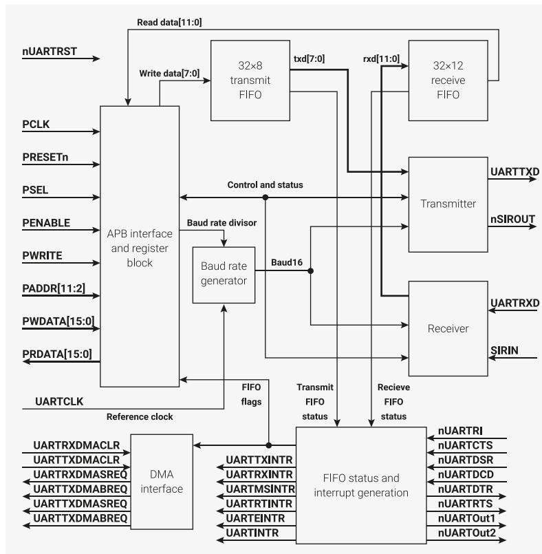
Figure 63. UART block diagram. Test logic is not shown for clarity.
12.1.2.3. Baud rate generator
The baud rate generator contains free-running counters that generate the internal clocks: Baud16 and IrLPBaud16 signals. Baud16 provides timing information for UART transmit and receive control. Baud16 is a stream of pulses with a width of one UARTCLK clock period and a frequency of 16 times the baud rate.
12.1.2.4. Transmit FIFO
The transmit FIFO is an 8-bit wide, 32 location deep, FIFO memory buffer. CPU data written across the APB interface is stored in the FIFO until read out by the transmit logic. When disabled, the transmit FIFO acts like a one byte holding register.
12.1.2.5. Receive FIFO
The receive FIFO is a 12-bit wide, 32 location deep, FIFO memory buffer. Received data and corresponding error bits are stored in the receive FIFO by the receive logic until read out by the CPU across the APB interface. When disabled, the receive FIFO acts like a one byte holding register.
12.1.2.6. Transmit logic
The transmit logic performs parallel-to-serial conversion on the data read from the transmit FIFO. Control logic outputs the serial bit stream in the following order:
- 1. Start bit
- 2. Data bits (Least Significant Bit (LSB) first)
- 3. Parity bit
- 4. Stop bits according to the programmed configuration in control registers
12.1.2.7. Receive logic
The receive logic performs serial-to-parallel conversion on the received bit stream after a valid start pulse has been detected. Receive logic includes overrun, parity, frame error checking, and line break detection; you can find the output of these checks in the status that accompanies the data written to the receive FIFO.
12.1.2.8. Interrupt generation logic
The UART generates individual maskable active HIGH interrupts to the processor interrupt controllers. To generate combined interrupts, the UART outputs an OR function of the individual interrupt requests.
For more information, see Section 12.1.6 .
12.1.2.9. DMA interface
The UART provides an interface to connect to the DMA controller as a UART DMA; for more information, see Section 12.1.5 .
12.1.2.10. Synchronizing registers and logic
The UART supports both asynchronous and synchronous operation of the clocks, PCLK and UARTCLK . The UART implements always-on synchronisation registers and handshaking logic. This has a minimal impact on performance and area. The UART performs control signal synchronisation on both directions of data flow (from the PCLK to the UARTCLK domain, and from the UARTCLK to the PCLK domain).
12.1.3. Operation
12.1.3.1. Clock signals
The frequency selected for UARTCLK must accommodate the required range of baud rates:
- • \( \text{FUARTCLK (min)} \geq 16 \times \text{baud\_rate (max)} \)
- • \( \text{FUARTCLK (max)} \leq 16 \times 65535 \times \text{baud\_rate (min)} \)
For example, for a range of baud rates from 110 baud to 460800 baud the UARTCLK frequency must be between 7.3728MHz to 115.34MHz.
To use all baud rates, the UARTCLK frequency must fall within the required error limits.
There is also a constraint on the ratio of clock frequencies for PCLK to UARTCLK . The frequency of UARTCLK must be no more than 5/3 times faster than the frequency of PCLK :
- • \( \text{FUARTCLK} \leq 5/3 \times \text{FPCLK} \)
For example, in UART mode, to generate 921600 baud when UARTCLK is 14.7456MHz, PCLK must be greater than or equal to 8.85276MHz. This ensures that the UART has sufficient time to write the received data to the receive FIFO.
12.1.3.2. UART operation
Control data is written to the UART Line Control Register, UARTLCR . This register is 30 bits wide internally, but provides external access through the APB interface by writes to the following registers:
- •
UARTLCR_H
, which defines the following:
- ◦ transmission parameters
- ◦ word length
- ◦ buffer mode
- ◦ number of transmitted stop bits
- ◦ parity mode
- ◦ break generation
- • UARTIBRD , which defines the integer baud rate divider
- • UARTFBRD , which defines the fractional baud rate divider
12.1.3.2.1. Fractional baud rate divider
The baud rate divisor is a 22-bit number consisting of a 16-bit integer and a 6-bit fractional part. The baud rate generator uses the baud rate divisor to determine the bit period. The fractional baud rate divider enables the use of any clock with a frequency greater than 3.6864MHz to act as UARTCLK , while it is still possible to generate all the standard baud rates.
The 16-bit integer is written to the Integer Baud Rate Register, UARTIBRD . The 6-bit fractional part is written to the Fractional Baud Rate Register, UARTFBRD . The Baud Rate Divisor has the following relationship to UARTCLK :
Baud Rate Divisor = \( \text{UARTCLK}/(16 \times \text{Baud Rate}) = BRD_I + BRD_F \) where \( BRD_I \) is the integer part and \( BRD_F \) is the fractional part separated by a decimal point as shown in Figure 64.
Figure 64. Baud rate divisor.

The diagram shows a rectangular box divided into two sections. The left section is labeled '16-bit integer' and the right section is labeled '6-bit fractional part'. A small black dot representing a decimal point is positioned between the two sections.
To calculate the 6-bit number (
\(
m
\)
), multiply the fractional part of the required baud rate divisor by 64 (
\(
2^n
\)
, where
\(
n
\)
is the width of the
UARTFBRD
register) and add 0.5 to account for rounding errors:
The UART generates an internal clock enable signal, Baud16. This is a stream of
UARTCLK
-wide pulses with an average frequency of 16 times the required baud rate. Divide this signal by 16 to give the transmit clock. A low number in the baud rate divisor produces a short bit period, and a high number in the baud rate divisor produces a long bit period.
12.1.3.2.2. Data transmission or reception
The UART uses two 32-byte FIFOs to store data received and transmitted. The receive FIFO has an extra four bits per character for status information. For transmission, data is written into the transmit FIFO. If the UART is enabled, it causes a data frame to start transmitting with the parameters indicated in the Line Control Register,
UARTLCR_H
. Data continues to be transmitted until there is no data left in the transmit FIFO. The
BUSY
signal goes HIGH immediately after data writes to the transmit FIFO (that is, the FIFO is non-empty) and remains asserted HIGH while data transmits.
BUSY
is negated only when the transmit FIFO is empty, and the last character has been transmitted from the shift register, including the stop bits.
BUSY
can be asserted HIGH even though the UART might no longer be enabled.
For each sample of data, three readings are taken and the majority value is kept. In the following paragraphs, the middle sampling point is defined, and one sample is taken either side of it.
When the receiver is idle (
UARTRXD
continuously 1, in the marking state) and a LOW is detected on the data input (a start bit has been received), the receive counter, with the clock enabled by Baud16, begins running and data is sampled on the eighth cycle of that counter in UART mode, or the fourth cycle of the counter in SIR mode to allow for the shorter logic 0 pulses (half way through a bit period).
The start bit is valid if
UARTRXD
is still LOW on the eighth cycle of Baud16, otherwise a false start bit is detected and it is ignored.
If the start bit was valid, successive data bits are sampled on every 16th cycle of Baud16 (that is, one bit period later) according to the programmed length of the data characters. The parity bit is then checked if parity mode was enabled.
Lastly, a valid stop bit is confirmed if
UARTRXD
is HIGH, otherwise a framing error has occurred. When a full word is received, the data is stored in the receive FIFO, with any error bits associated with that word
12.1.3.2.3. Error bits
The receive FIFO stores three error bits in bits 8 (framing), 9 (parity), and 10 (break), each associated with a particular character. An additional error bit, stored in bit 11 of the receive FIFO, indicates an overrun error.
12.1.3.2.4. Overrun bit
The overrun bit is not associated with the character in the receive FIFO. The overrun error is set when the FIFO is full and the next character is completely received in the shift register. The data in the shift register is overwritten, but it is not written into the FIFO. When an empty location becomes available in the FIFO, another character is received and the state of the overrun bit is copied into the receive FIFO along with the received character. The overrun state is then cleared. Table 1025 lists the bit functions of the receive FIFO.
Table 1025. Receive
FIFO bit functions
| FIFO bit | Function |
|---|---|
| 11 | Overrun indicator |
| 10 | Break error |
| 9 | Parity error |
| 8 | Framing error |
| 7:0 | Received data |
12.1.3.2.5. Disabling the FIFOs
The bottom entry of the transmit and receive sides of the UART both have the equivalent of a 1-byte holding register. You can manipulate flags to disable the FIFOs, allowing you to use the bottom entry of the FIFOs as a 1-byte register. However, this doesn't physically disable the FIFOs. When using the FIFOs as a 1-byte register, a write to the data register bypasses the holding register unless the transmit shift register is already in use.
12.1.3.2.6. System and diagnostic loopback testing
To perform loopback testing for UART data, set the Loop Back Enable (LBE) bit to 1 in the Control Register,
UARTCR
. Data transmitted on
UARTTXD
is received on the
UARTRXD
input.
12.1.3.3. UART character frame
Figure 65. UART
character frame.
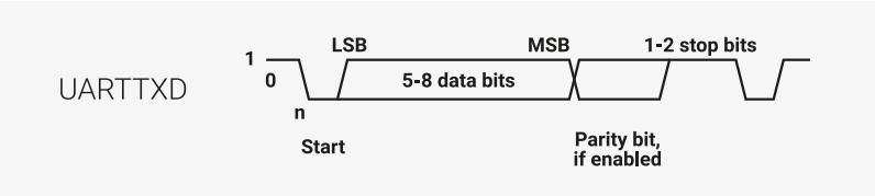
The diagram illustrates the UART character frame structure. It begins with a 'Start' bit, represented by a low pulse (0) on the
UARTTXD
line. This is followed by '5-8 data bits', with the 'LSB' (Least Significant Bit) at the beginning and the 'MSB' (Most Significant Bit) at the end. A 'Parity bit, if enabled' follows the data bits. The frame concludes with '1-2 stop bits', represented by high pulses (1). A label 'n' is placed below the start bit.
12.1.4. UART hardware flow control
The fully-selectable hardware flow control feature enables you to control the serial data flow with the
nUARTRTS
output and
nUARTCTS
input signals. Figure 66 shows how to communicate between two devices using hardware flow control:
Figure 66. Hardware
flow control between
two similar devices.
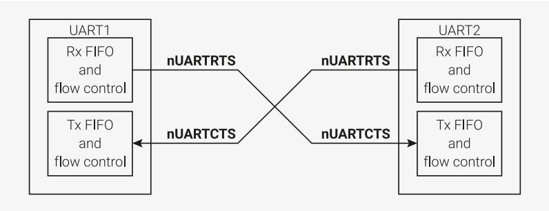
The diagram shows two UART devices,
UART1
and
UART2
, each containing an 'Rx FIFO and flow control' block and a 'Tx FIFO and flow control' block. The
nUARTRTS
signal from
UART1
's Tx FIFO is connected to
UART2
's Rx FIFO. Conversely, the
nUARTCTS
signal from
UART2
's Tx FIFO is connected to
UART1
's Rx FIFO.
When the RTS flow control is enabled,
nUARTRTS
is asserted until the receive FIFO is filled up to the programmed watermark level. When the CTS flow control is enabled, the transmitter can only transmit data when
nUARTCTS
is asserted.
The hardware flow control is selectable using the
RTSEn
and
CTSEn
bits in the Control Register,
UARTCR
. Table 1026 shows how to configure
UARTCR
register bits to enable RTS and/or CTS.
Table 1026. Control bits to enable and disable hardware flow control.
| UARTCR register bits | ||
|---|---|---|
| CTSEn | RTSEn | Description |
| 1 | 1 | Both RTS and CTS flow control enabled |
| 1 | 0 | Only CTS flow control enabled |
| 0 | 1 | Only RTS flow control enabled |
| 0 | 0 | Both RTS and CTS flow control disabled |
NOTE
When RTS flow control is enabled, the software cannot use the RTSEn bit in the Control Register (UARTCR) to control the status of nUARTRTS.
12.1.4.1. RTS flow control
The RTS flow control logic is linked to the programmable receive FIFO watermark levels.
When RTS flow control is disabled, the receive FIFO receives data until full, or no more data is transmitted to it.
When RTS flow control is enabled, the nUARTRTS is asserted until the receive FIFO fills up to the watermark level. When the receive FIFO reaches the watermark level, the nUARTRTS signal is de-asserted. This indicates that the FIFO has no more room to receive data. The transmission of data is expected to cease after the current character has been transmitted. When the receive FIFO drains below the watermark level, the nUARTRTS signal is reasserted.
12.1.4.2. CTS flow control
The CTS flow control logic is linked to the nUARTCTS signal.
When CTS flow control is disabled, the transmitter transmits data until the transmit FIFO is empty.
When CTS flow control is enabled, the transmitter checks the nUARTCTS signal before transmitting each byte. It only transmits the byte if the nUARTCTS signal is asserted. As long as the transmit FIFO is not empty and nUARTCTS is asserted, data continues to transmit. If the transmit FIFO is empty and the nUARTCTS signal is asserted, no data is transmitted. If the nUARTCTS signal is de-asserted during transmission, the transmitter finishes transmitting the current character before stopping.
12.1.5. UART DMA interface
The UART provides an interface to connect to a DMA controller. The DMA operation of the UART is controlled using the DMA Control Register, UARTRDMACR. The DMA interface includes the following signals:
For receive:
UARTRXDMASREQ
Single character DMA transfer request, asserted by the UART. For receive, one character consists of up to 12 bits. This signal is asserted when the receive FIFO contains at least one character.
UARTRXDMABREQ
Burst DMA transfer request, asserted by the UART. This signal is asserted when the receive FIFO contains more characters than the programmed watermark level. You can program the watermark level for each FIFO using the Interrupt FIFO Level Select Register (UARTIFLS).
UARTEINTR . It enables the DMA receive request outputs, UARTRXDMASREQ or UARTRXDMABREQ , to be masked out when the UART error interrupt, UARTEINTR , is asserted. The DMA receive request outputs remain inactive until the UARTEINTR is cleared. The DMA transmit request outputs are unaffected.
Figure 67. DMA transfer waveforms.

The figure is a timing diagram showing four digital signals over time. The top signal is PCLK, a periodic square wave. Below it are three signals: DMASREQ, DMABREQ, and DMACLR. DMASREQ and DMABREQ are active-low signals that pulse low for several clock cycles. DMACLR is an active-low signal that pulses low for a single clock cycle. All signals are synchronous to the PCLK clock.
Figure 67 shows the timing diagram for both a single transfer request and a burst transfer request with the appropriate DMACLR signal. The signals are all synchronous to PCLK. For the sake of clarity it is assumed that there is no synchronization of the request signals in the DMA controller.
12.1.6. Interrupts
There are eleven maskable interrupts generated in the UART. On RP2350, only the combined interrupt output, UARTINTR , is connected.
To enable or disable individual interrupts, change the mask bits in the Interrupt Mask Set/Clear Register, UARTIMSC . Set the appropriate mask bit HIGH to enable the interrupt.
The transmit and receive dataflow interrupts UARTRXINTR and UARTTXINTR have been separated from the status interrupts. This enables you to use UARTRXINTR and UARTTXINTR to read or write data in response to FIFO trigger levels.
The error interrupt, UARTEINTR , can be triggered when there is an error in the reception of data. A number of error conditions are possible.
The modem status interrupt, UARTMSINTR , is a combined interrupt of all the individual modem status signals.
The status of the individual interrupt sources can be read either from the Raw Interrupt Status Register, UARTRIS , or from the Masked Interrupt Status Register, UARTMIS .
12.1.6.1. UARTMSINTR
The modem status interrupt is asserted if any of the modem status signals ( nUARTCTS , nUARTDCD , nUARTDSR , and nUARTRI ) change. To clear the modem status interrupt, write a 1 to the bits corresponding to the modem status signals that generated the interrupt in the Interrupt Clear Register ( UARTICR ).
12.1.6.2. UARTRXINTR
The receive interrupt changes state when one of the following events occurs:
- • The FIFOs are enabled and the receive FIFO reaches the programmed trigger level. This asserts the receive interrupt HIGH. To clear the receive interrupt, read data from the receive FIFO until it drops below the trigger level.
- • The FIFOs are disabled (have a depth of one location) and data is received, thereby filling the receive FIFO. This asserts the receive interrupt HIGH. To clear the receive interrupt, perform a single read from the receive FIFO.
In both cases, you can also clear the interrupt manually.
12.1.6.3. UARTTXINTR
The transmit interrupt changes state when one of the following events occurs:
- • The FIFOs are enabled and the transmit FIFO is equal to or lower than the programmed trigger level. This asserts the transmit interrupt HIGH. To clear the transmit interrupt, write data to the transmit FIFO until it exceeds the
trigger level.
- • The FIFOs are disabled (have a depth of one location) and there is no data present in the transmit FIFO. This asserts the transmit interrupt HIGH. To clear the transmit interrupt, perform a single write to the transmit FIFO.
In both cases, you can also clear the interrupt manually.
To update the transmit FIFO, write data to the transmit FIFO before or after enabling the UART and the interrupts.
i NOTE
The transmit interrupt is based on a transition through a level, rather than on the level itself. When the interrupt and the UART is enabled before any data is written to the transmit FIFO, the interrupt is not set. The interrupt is only set after written data leaves the single location of the transmit FIFO and it becomes empty.
12.1.6.4. UARTRINTR
The receive timeout interrupt is asserted when the receive FIFO is not empty and no more data is received during a 32-bit period.
The receive timeout interrupt is cleared in the following scenarios:
- • the FIFO becomes empty through reading all the data or by reading the holding register
- • a 1 is written to the corresponding bit of the Interrupt Clear Register, UARTICR
12.1.6.5. UARTEINTR
The error interrupt is asserted when an error occurs in the reception of data by the UART. The interrupt can be caused by a number of different error conditions:
- • framing
- • parity
- • break
- • overrun
To determine the cause of the interrupt, read the Raw Interrupt Status Register ( UARTISR ) or the Masked Interrupt Status Register ( UARTMIS ). To clear the interrupt, write to the relevant bits of the Interrupt Clear Register, UARTICR (bits 7 to 10 are the error clear bits).
12.1.6.6. UARTINTR
The interrupts are also combined into a single output, that is an OR function of the individual masked sources. You can connect this output to a system interrupt controller to provide another level of masking on a individual peripheral basis.
The combined UART interrupt is asserted if any of the individual interrupts are asserted and enabled.
12.1.7. Programmer's model
The SDK provides a uart_init function to configure the UART with a particular baud rate. Once the UART is initialised, the user must configure a GPIO pin as UART_TX and UART_RX . See Section 9.10.1 for more information on selecting a GPIO function.
To initialise the UART, the uart_init function takes the following steps:
- 1. De-asserts the reset
- 2. Enables
clk_peri - 3. Sets enable bits in the control register
- 4. Enables the FIFOs
- 5. Sets the baud rate divisors
- 6. Sets the format
SDK: https://github.com/raspberrypi/pico-sdk/blob/master/src/rp2_common/hardware_uart/uart.c Lines 42 - 92
42 uint uart_init(uart_inst_t *uart, uint baudrate) {
43     invalid_params_if(HARDWARE_UART, uart != uart0 && uart != uart1);
44
45     if (uart_clock_get_hz(uart) == 0) {
46         return 0;
47     }
48
49     uart_reset(uart);
50     uart_unreset(uart);
51
52     uart_set_translate_crlf(uart, PICO_UART_DEFAULT_CRLF);
53
54     // Any LCR writes need to take place before enabling the UART
55     uint baud = uart_set_baudrate(uart, baudrate);
56
57     // inline the uart_set_format() call, as we don't need the CR disable/re-enable
58     // protection, and also many people will never call it again, so having
59     // the generic function is not useful, and much bigger than this inlined
60     // code which is only a handful of instructions.
61     //
62     // The UART_UARTLCR_H_FEN_BITS setting is combined as well as it is the same register
63     #ifdef 0
64         uart_set_format(uart, 8, 1, UART_PARITY_NONE);
65         // Enable FIFOs (must be before setting UARTEN, as this is an LCR access)
66         hw_set_bits(&uart_get_hw(uart)->lcr_h, UART_UARTLCR_H_FEN_BITS);
67     #else
68         uint data_bits = 8;
69         uint stop_bits = 1;
70         uint parity = UART_PARITY_NONE;
71         hw_write_masked(&uart_get_hw(uart)->lcr_h,
72             (((data_bits - 5u) << UART_UARTLCR_H_WLEN_LSB) |
73              ((stop_bits - 1u) << UART_UARTLCR_H_STP2_LSB) |
74              (bool_to_bit(parity != UART_PARITY_NONE) << UART_UARTLCR_H_PEN_LSB) |
75              (bool_to_bit(parity == UART_PARITY_EVEN) << UART_UARTLCR_H_EPS_LSB) |
76              UART_UARTLCR_H_FEN_BITS,
77              UART_UARTLCR_H_WLEN_BITS | UART_UARTLCR_H_STP2_BITS |
78              UART_UARTLCR_H_PEN_BITS | UART_UARTLCR_H_EPS_BITS |
79              UART_UARTLCR_H_FEN_BITS);
80     #endif
81
82     // Enable the UART, both TX and RX
83     uart_get_hw(uart)->cr = UART_UARTCR_UARTEN_BITS | UART_UARTCR_TXE_BITS |
        UART_UARTCR_RXE_BITS;
84     // Always enable DREQ signals -- no harm in this if DMA is not listening
85     uart_get_hw(uart)->dmacr = UART_UARTDMACR_TXDMAE_BITS | UART_UARTDMACR_RXDMAE_BITS;
86
87     return baud;
88 }
12.1.7.1. Baud rate calculation
The UART baud rate is derived from dividing
clk_peri
.
If the required baud rate is 115200 and UARTCLK = 125MHz then:
Baud Rate Divisor = \( (125 \times 10^6)/(16 \times 115200) \sim 67.817 \)
Therefore, BRDI = 67 and BRDF = 0.817,
Therefore, fractional part, m = integer((0.817 × 64) + 0.5) = 52
Generated baud rate divider = 67 + 52/64 = 67.8125
Generated baud rate = \( (125 \times 10^6)/(16 \times 67.8125) \sim 115207 \)
Error = \( (\text{abs}(115200 - 115207) / 115200) \times 100 \sim 0.006\% \)
SDK: https://github.com/raspberrypi/pico-sdk/blob/master/src/rp2_common/hardware_uart/uart.c Lines 155 - 180
155 uint uart_set_baudrate(uart_inst_t *uart, uint baudrate) {
156     invalid_params_if(HARDWARE_UART, baudrate == 0);
157     uint32_t baud_rate_div = (8 * uart_clock_get_hz(uart) / baudrate) + 1;
158     uint32_t baud_ibrd = baud_rate_div >> 7;
159     uint32_t baud_fbrd;
160
161     if (baud_ibrd == 0) {
162         baud_ibrd = 1;
163         baud_fbrd = 0;
164     } else if (baud_ibrd >= 65535) {
165         baud_ibrd = 65535;
166         baud_fbrd = 0;
167     } else {
168         baud_fbrd = (baud_rate_div & 0x7f) >> 1;
169     }
170
171     uart_get_hw(uart)->ibrd = baud_ibrd;
172     uart_get_hw(uart)->fbrd = baud_fbrd;
173
174     // PL011 needs a (dummy) LCR_H write to latch in the divisors.
175     // We don't want to actually change LCR_H contents here.
176     uart_write_lcr_bits_masked(uart, 0, 0);
177
178     // See datasheet
179     return (4 * uart_clock_get_hz(uart)) / (64 * baud_ibrd + baud_fbrd);
180 }
12.1.8. List of registers
The UART0 and UART1 registers start at base addresses of
0x40070000
and
0x40078000
respectively (defined as
UART0_BASE
and
UART1_BASE
in SDK).
Table 1028. List of UART registers
| Offset | Name | Info |
|---|---|---|
| 0x000 | UARTDR | Data Register, UARTDR |
| 0x004 | UARTRSR | Receive Status Register/Error Clear Register, UARTRSR/UARTECR |
| 0x018 | UARTFR | Flag Register, UARTFR |
| 0x020 | UARTILPR | IrDA Low-Power Counter Register, UARTILPR |
| Offset | Name | Info |
|---|---|---|
| 0x024 | UARTIBRD | Integer Baud Rate Register, UARTIBRD |
| 0x028 | UARTFBRD | Fractional Baud Rate Register, UARTFBRD |
| 0x02c | UARTLCR_H | Line Control Register, UARTLCR_H |
| 0x030 | UARTCR | Control Register, UARTCR |
| 0x034 | UARTIFLS | Interrupt FIFO Level Select Register, UARTIFLS |
| 0x038 | UARTIMSC | Interrupt Mask Set/Clear Register, UARTIMSC |
| 0x03c | UARTRIS | Raw Interrupt Status Register, UARTRIS |
| 0x040 | UARTMIS | Masked Interrupt Status Register, UARTMIS |
| 0x044 | UARTICR | Interrupt Clear Register, UARTICR |
| 0x048 | UARTDMACR | DMA Control Register, UARTDMACR |
| 0xfe0 | UARTPERIPHID0 | UARTPeriphID0 Register |
| 0xfe4 | UARTPERIPHID1 | UARTPeriphID1 Register |
| 0xfe8 | UARTPERIPHID2 | UARTPeriphID2 Register |
| 0xfec | UARTPERIPHID3 | UARTPeriphID3 Register |
| 0xff0 | UARTPCELLID0 | UARTPCellID0 Register |
| 0xff4 | UARTPCELLID1 | UARTPCellID1 Register |
| 0xff8 | UARTPCELLID2 | UARTPCellID2 Register |
| 0xffc | UARTPCELLID3 | UARTPCellID3 Register |
UART: UARTDR Register
Offset: 0x000
Description
Data Register, UARTDR
Table 1029. UARTDR Register
| Bits | Description | Type | Reset |
|---|---|---|---|
| 31:12 | Reserved. | - | - |
| 11 | OE: Overrun error. This bit is set to 1 if data is received and the receive FIFO is already full. This is cleared to 0 once there is an empty space in the FIFO and a new character can be written to it. | RO | - |
| 10 | BE: Break error. This bit is set to 1 if a break condition was detected, indicating that the received data input was held LOW for longer than a full-word transmission time (defined as start, data, parity and stop bits). In FIFO mode, this error is associated with the character at the top of the FIFO. When a break occurs, only one 0 character is loaded into the FIFO. The next character is only enabled after the receive data input goes to a 1 (marking state), and the next valid start bit is received. | RO | - |
| 9 | PE: Parity error. When set to 1, it indicates that the parity of the received data character does not match the parity that the EPS and SPS bits in the Line Control Register, UARTLCR_H. In FIFO mode, this error is associated with the character at the top of the FIFO. | RO | - |
| Bits | Description | Type | Reset |
|---|---|---|---|
| 8 | FE: Framing error. When set to 1, it indicates that the received character did not have a valid stop bit (a valid stop bit is 1). In FIFO mode, this error is associated with the character at the top of the FIFO. | RO | - |
| 7:0 | DATA: Receive (read) data character. Transmit (write) data character. | RWF | - |
UART: UARTRSR Register
Offset: 0x004
Description
Receive Status Register/Error Clear Register, UARTRSR/UARTECR
Table 1030. UARTRSR Register
| Bits | Description | Type | Reset |
|---|---|---|---|
| 31:4 | Reserved. | - | - |
| 3 | OE: Overrun error. This bit is set to 1 if data is received and the FIFO is already full. This bit is cleared to 0 by a write to UARTECR. The FIFO contents remain valid because no more data is written when the FIFO is full, only the contents of the shift register are overwritten. The CPU must now read the data, to empty the FIFO. | WC | 0x0 |
| 2 | BE: Break error. This bit is set to 1 if a break condition was detected, indicating that the received data input was held LOW for longer than a full-word transmission time (defined as start, data, parity, and stop bits). This bit is cleared to 0 after a write to UARTECR. In FIFO mode, this error is associated with the character at the top of the FIFO. When a break occurs, only one 0 character is loaded into the FIFO. The next character is only enabled after the receive data input goes to a 1 (marking state) and the next valid start bit is received. | WC | 0x0 |
| 1 | PE: Parity error. When set to 1, it indicates that the parity of the received data character does not match the parity that the EPS and SPS bits in the Line Control Register, UARTLCR_H. This bit is cleared to 0 by a write to UARTECR. In FIFO mode, this error is associated with the character at the top of the FIFO. | WC | 0x0 |
| 0 | FE: Framing error. When set to 1, it indicates that the received character did not have a valid stop bit (a valid stop bit is 1). This bit is cleared to 0 by a write to UARTECR. In FIFO mode, this error is associated with the character at the top of the FIFO. | WC | 0x0 |
UART: UARTFR Register
Offset: 0x018
Description
Flag Register, UARTFR
Table 1031. UARTFR Register
| Bits | Description | Type | Reset |
|---|---|---|---|
| 31:9 | Reserved. | - | - |
| 8 | RI: Ring indicator. This bit is the complement of the UART ring indicator, nUARTRI, modem status input. That is, the bit is 1 when nUARTRI is LOW. | RO | - |
| Bits | Description | Type | Reset |
|---|---|---|---|
| 7 | TXFE : Transmit FIFO empty. The meaning of this bit depends on the state of the FEN bit in the Line Control Register, UARTLCR_H. If the FIFO is disabled, this bit is set when the transmit holding register is empty. If the FIFO is enabled, the TXFE bit is set when the transmit FIFO is empty. This bit does not indicate if there is data in the transmit shift register. | RO | 0x1 |
| 6 | RXFF : Receive FIFO full. The meaning of this bit depends on the state of the FEN bit in the UARTLCR_H Register. If the FIFO is disabled, this bit is set when the receive holding register is full. If the FIFO is enabled, the RXFF bit is set when the receive FIFO is full. | RO | 0x0 |
| 5 | TXFF : Transmit FIFO full. The meaning of this bit depends on the state of the FEN bit in the UARTLCR_H Register. If the FIFO is disabled, this bit is set when the transmit holding register is full. If the FIFO is enabled, the TXFF bit is set when the transmit FIFO is full. | RO | 0x0 |
| 4 | RXFE : Receive FIFO empty. The meaning of this bit depends on the state of the FEN bit in the UARTLCR_H Register. If the FIFO is disabled, this bit is set when the receive holding register is empty. If the FIFO is enabled, the RXFE bit is set when the receive FIFO is empty. | RO | 0x1 |
| 3 | BUSY : UART busy. If this bit is set to 1, the UART is busy transmitting data. This bit remains set until the complete byte, including all the stop bits, has been sent from the shift register. This bit is set as soon as the transmit FIFO becomes non-empty, regardless of whether the UART is enabled or not. | RO | 0x0 |
| 2 | DCD : Data carrier detect. This bit is the complement of the UART data carrier detect, nUARTDCD, modem status input. That is, the bit is 1 when nUARTDCD is LOW. | RO | - |
| 1 | DSR : Data set ready. This bit is the complement of the UART data set ready, nUARTDSR, modem status input. That is, the bit is 1 when nUARTDSR is LOW. | RO | - |
| 0 | CTS : Clear to send. This bit is the complement of the UART clear to send, nUARTCTS, modem status input. That is, the bit is 1 when nUARTCTS is LOW. | RO | - |
UART: UARTILPR Register
Offset: 0x020
Description
IrDA Low-Power Counter Register, UARTILPR
Table 1032. UARTILPR Register
| Bits | Description | Type | Reset |
|---|---|---|---|
| 31:8 | Reserved. | - | - |
| 7:0 | ILPDVSR : 8-bit low-power divisor value. These bits are cleared to 0 at reset. | RW | 0x00 |
UART: UARTIBRD Register
Offset: 0x024
Description
Integer Baud Rate Register, UARTIBRD
Table 1033. UARTIBRD Register
| Bits | Description | Type | Reset |
|---|---|---|---|
| 31:16 | Reserved. | - | - |
| Bits Register 31:21 20 19:16 15:12 11:0 | column_2 | Description ARCHITECT : Defines the architect of the component. Bits [31:28] are the PRESENT : Defines that the DEVARCH register is present REVISION : Defines the architecture revision of the component ARCHVER : Defines the architecture version of the component ARCHPART : Defines the architecture of the component | Type RO RO RO RO RO | Reset 0x23b 0x1 0x0 0x1 0xa02 |
|---|---|---|---|---|
| 31:6 | Reserved. | - | - | |
| 5:0 | BAUD_DIVFRAC | : The fractional baud rate divisor. These bits are cleared to 0 on reset. : UARTLCR_H Register | RW | 0x00 |
| Bits | Description | Type | Reset | |
| 31:8 | Reserved. | - | - | |
| 7 | SPS | : Stick parity select. 0 = stick parity is disabled 1 = either: * if the EPS bit is the PEN bit disables parity checking and generation. | RW | 0x0 |
| 6:5 | WLEN bits. | : Word length. These bits indicate the number of data bits transmitted or | RW | 0x0 |
| 4 | FEN | : Enable FIFOs: 0 = FIFOs are disabled (character mode) that is, the FIFOs are enabled (FIFO mode). | RW | 0x0 |
| 3 | STP2 | : Two stop bits select. If this bit is set to 1, two stop bits are transmitted at the end of the frame. The receive logic does not check for two stop bits being received. | RW | 0x0 |
| 2 | EPS | : Even parity select. Controls the type of parity the UART uses during an odd number of 1s in the data and parity bits. 1 = even parity. The UART bit has no effect when the PEN bit disables parity checking and generation. | RW | 0x0 |
| 1 | PEN | : Parity enable: 0 = parity is disabled and no parity bit added to the data frame 1 = parity checking and generation is enabled. | RW | 0x0 |
| 0 | BRK | : Send break. If this bit is set to 1, a low-level is continually output on the | RW | 0x0 |
UART: UARTFBRD Register
Offset: 0x028
Description
Fractional Baud Rate Register, UARTFBRD
Table 1034.
UARTFBRD Register
UART: UARTLCR_H Register
Offset: 0x02c
Description
Line Control Register, UARTLCR_H
Table 1035.
UARTLCR_H Register
UART: UARTCR Register
Offset: 0x030
DescriptionControl Register, UARTCR
Table 1036. UARTCR Register
| Bits Register 31:21 20 19:16 15:12 11:0 | column_2 | Description ARCHITECT : Defines the architect of the component. Bits [31:28] are the PRESENT : Defines that the DEVARCH register is present REVISION : Defines the architecture revision of the component ARCHVER : Defines the architecture version of the component ARCHPART : Defines the architecture of the component | Type RO RO RO RO RO | Reset 0x23b 0x1 0x0 0x1 0xa02 |
|---|---|---|---|---|
| 31:16 | Reserved. | - | - | |
| 15 | CTSEN | : CTS hardware flow control enable. If this bit is set to 1, CTS hardware asserted. | RW | 0x0 |
| 14 | RTSEN | : RTS hardware flow control enable. If this bit is set to 1, RTS hardware flow control is enabled. Data is only requested when there is space in the receive FIFO for it to be received. | RW | 0x0 |
| 13 | OUT2 | : This bit is the complement of the UART Out2 (nUARTOut2) modem DTE this can be used as Ring Indicator (RI). | RW | 0x0 |
| 12 | OUT1 | : This bit is the complement of the UART Out1 (nUARTOut1) modem DTE this can be used as Data Carrier Detect (DCD). | RW | 0x0 |
| 11 | RTS | : Request to send. This bit is the complement of the UART request to to a 1 then nUARTRTS is LOW. | RW | 0x0 |
| 10 | DTR | : Data transmit ready. This bit is the complement of the UART data transmit ready, nUARTDTR, modem status output. That is, when the bit is programmed to a 1 then nUARTDTR is LOW. | RW | 0x0 |
| 9 | RXE | : Receive enable. If this bit is set to 1, the receive section of the UART is enabled. Data reception occurs for either UART signals or SIR signals middle of reception, it completes the current character before stopping. | RW | 0x1 |
| 8 | TXE | : Transmit enable. If this bit is set to 1, the transmit section of the UART is enabled. Data transmission occurs for either UART signals, or SIR signals | RW | 0x1 |
| 7 | LBE | : Loopback enable. If this bit is set to 1 and the SIREN bit is set to 1 and the SIRTEST bit in the Test Control Register, UARTTCR is set to 1, then the in the test register must be set to 1 to override the normal half-duplex SIR operation. This must be the requirement for accessing the test registers | RW | 0x0 |
| 6:3 | Reserved. | - | - |
| Bits 14:10 9:5 4:0 Bits | Description SHIFT Description | MASK_MSB : The most-significant bit allowed to pass by the mask (inclusive) MASK_LSB : The least-significant bit allowed to pass by the mask (inclusive) : Right-rotate applied to accumulator before masking. By appropriately | Type RW RW RW Type | Reset 0x00 0x00 0x00 Reset |
|---|---|---|---|---|
| 31:6 | Reserved. | - | - | |
| 5:3 | RXIFLSEL | : Receive interrupt FIFO level select. The trigger points for the receive interrupt are as follows: b000 = Receive FIFO becomes >= 1 / 8 full b001 = | RW | 0x2 |
| 2:0 | TXIFLSEL | / 8 full b101-b111 = reserved. : Transmit interrupt FIFO level select. The trigger points for the | RW | 0x2 |
| Table 1038. Bits UARTIMSC Register | Description | Type | Reset | |
| 31:11 | Reserved. | - | - | |
| 10 | OEIM : Overrun error interrupt mask. A read returns the current mask for the | RW | 0x0 |
UART: UARTIFLS Register
Offset: 0x034
Description
Interrupt FIFO Level Select Register, UARTIFLS
Table 1037. UARTIFLS Register
UART: UARTIMSC Register
Offset: 0x038
Description
Interrupt Mask Set/Clear Register, UARTIMSC
Table 1038. UARTIMSC Register
| Bits 23:16 15:8 7:0 Bits 31:24 | column_2 | Description ATTR2 : Memory attribute encoding for MPU regions with an AttrIndex of 2 ATTR1 : Memory attribute encoding for MPU regions with an AttrIndex of 1 ATTR0 : Memory attribute encoding for MPU regions with an AttrIndex of 0 Description ATTR7 : Memory attribute encoding for MPU regions with an AttrIndex of 7 | Type RW RW RW Type RW | Reset 0x00 0x00 0x00 Reset 0x00 | Description |
|---|---|---|---|---|---|
| 4 | RXIM | : Receive interrupt mask. A read returns the current mask for the is set. A write of 0 clears the mask. | RW | 0x0 | Table 388. PMPCFG3 |
| 3 | DSRMIM | : nUARTDSR modem interrupt mask. A read returns the current mask for the UARTDSRINTR interrupt. On a write of 1, the mask of the UARTDSRINTR interrupt is set. A write of 0 clears the mask. | RW | 0x0 | Table 388. PMPCFG3 |
| 2 | DCDMIM | : nUARTDCD modem interrupt mask. A read returns the current mask for the UARTDCDINTR interrupt. On a write of 1, the mask of the UARTDCDINTR interrupt is set. A write of 0 clears the mask. | RW | 0x0 | Table 388. PMPCFG3 |
| 1 | CTSMIM | : nUARTCTS modem interrupt mask. A read returns the current mask for the UARTCTSINTR interrupt. On a write of 1, the mask of the UARTCTSINTR interrupt is set. A write of 0 clears the mask. | RW | 0x0 | Table 388. PMPCFG3 |
| 0 | RIMIM | : nUARTRI modem interrupt mask. A read returns the current mask for the UARTRIINTR interrupt. On a write of 1, the mask of the UARTRIINTR interrupt is set. A write of 0 clears the mask. | RW | 0x0 | Table 388. PMPCFG3 |
| Bits | Description | Type | Reset | Offset : 0x03c Description Raw Interrupt Status Register, UARTRIS Table 1039. UARTRIS | |
| 31:11 | Reserved. | - | - | Register | |
| 10 | OERIS | : Overrun error interrupt status. Returns the raw interrupt state of the UARTOEINTR interrupt. | RO | 0x0 | Register |
| 9 | BERIS | : Break error interrupt status. Returns the raw interrupt state of the UARTBEINTR interrupt. | RO | 0x0 | Register |
| 8 | PERIS | : Parity error interrupt status. Returns the raw interrupt state of the UARTPEINTR interrupt. | RO | 0x0 | Register |
UART: UARTRIS Register
Offset: 0x03c
Description
Raw Interrupt Status Register, UARTRIS
Table 1039. UARTRIS Register
| Bits 23:16 15:8 7:0 Bits 31:24 | column_2 | Description ATTR2 : Memory attribute encoding for MPU regions with an AttrIndex of 2 ATTR1 : Memory attribute encoding for MPU regions with an AttrIndex of 1 ATTR0 : Memory attribute encoding for MPU regions with an AttrIndex of 0 Description ATTR7 : Memory attribute encoding for MPU regions with an AttrIndex of 7 | Type RW RW RW Type RW | Reset 0x00 0x00 0x00 Reset 0x00 | Description |
|---|---|---|---|---|---|
| 3 | DSRRMIS | : nUARTDSR modem interrupt status. Returns the raw interrupt state of the UARTDSRINTR interrupt. | RO | - | Register |
| 2 | DCDRMIS | : nUARTDCD modem interrupt status. Returns the raw interrupt state of the UARTDCDINTR interrupt. | RO | - | Register |
| 1 | CTSRMIS | : nUARTCTS modem interrupt status. Returns the raw interrupt state of the UARTCTSINTR interrupt. | RO | - | Register |
| 0 | RIRMIS | : nUARTRI modem interrupt status. Returns the raw interrupt state of the UARTRIINTR interrupt. | RO | - | Register |
| Bits | Description | Type | Reset | Offset : 0x040 Description Masked Interrupt Status Register, UARTMIS Table 1040. UARTMIS | |
| 31:11 | Reserved. | - | - | Register | |
| 10 | OEMIS | : Overrun error masked interrupt status. Returns the masked interrupt state of the UARTOEINTR interrupt. | RO | 0x0 | Register |
| 9 | BEMIS | : Break error masked interrupt status. Returns the masked interrupt state of the UARTBEINTR interrupt. | RO | 0x0 | Register |
| 8 | PEMIS | : Parity error masked interrupt status. Returns the masked interrupt state of the UARTPEINTR interrupt. | RO | 0x0 | Register |
| 7 | FEMIS | : Framing error masked interrupt status. Returns the masked interrupt state of the UARTFEINTR interrupt. | RO | 0x0 | Register |
| 6 | RTMIS | : Receive timeout masked interrupt status. Returns the masked interrupt state of the UARTRTINTR interrupt. | RO | 0x0 | Register |
| 5 | TXMIS | : Transmit masked interrupt status. Returns the masked interrupt state of the UARTTXINTR interrupt. | RO | 0x0 | Register |
| 4 | RXMIS | : Receive masked interrupt status. Returns the masked interrupt state of the UARTRXINTR interrupt. | RO | 0x0 | Register |
| 3 | DSRMMIS | : nUARTDSR modem masked interrupt status. Returns the masked interrupt state of the UARTDSRINTR interrupt. | RO | - | Register |
| 2 | DCDMMIS | : nUARTDCD modem masked interrupt status. Returns the masked interrupt state of the UARTDCDINTR interrupt. | RO | - | Register |
UART: UARTMIS Register
Offset: 0x040
Description
Masked Interrupt Status Register, UARTMIS
Table 1040. UARTMIS Register
| Bits | Description | Type | Reset |
|---|---|---|---|
| 1 | CTSMMIS : nUARTCTS modem masked interrupt status. Returns the masked interrupt state of the UARTCTSINTR interrupt. | RO | - |
| 0 | RIMMIS : nUARTRI modem masked interrupt status. Returns the masked interrupt state of the UARTRIINTR interrupt. | RO | - |
UART: UARTICR Register
Offset: 0x044
Description
Interrupt Clear Register, UARTICR
Table 1041. UARTICR Register
| Bits | Description | Type | Reset |
|---|---|---|---|
| 31:11 | Reserved. | - | - |
| 10 | OEIC : Overrun error interrupt clear. Clears the UARTOEINTR interrupt. | WC | - |
| 9 | BEIC : Break error interrupt clear. Clears the UARTBEINTR interrupt. | WC | - |
| 8 | PEIC : Parity error interrupt clear. Clears the UARTPEINTR interrupt. | WC | - |
| 7 | FEIC : Framing error interrupt clear. Clears the UARTFEINTR interrupt. | WC | - |
| 6 | RTIC : Receive timeout interrupt clear. Clears the UARTRTINTR interrupt. | WC | - |
| 5 | TXIC : Transmit interrupt clear. Clears the UARTTXINTR interrupt. | WC | - |
| 4 | RXIC : Receive interrupt clear. Clears the UARTRXINTR interrupt. | WC | - |
| 3 | DSRMIC : nUARTDSR modem interrupt clear. Clears the UARTDSRINTR interrupt. | WC | - |
| 2 | DCDMIC : nUARTDCD modem interrupt clear. Clears the UARTDCDINTR interrupt. | WC | - |
| 1 | CTSMIC : nUARTCTS modem interrupt clear. Clears the UARTCTSINTR interrupt. | WC | - |
| 0 | RIMIC : nUARTRI modem interrupt clear. Clears the UARTRIINTR interrupt. | WC | - |
UART: UARTDMACR Register
Offset: 0x048
Description
DMA Control Register, UARTDMACR
Table 1042. UARTDMACR Register
| Bits | Description | Type | Reset |
|---|---|---|---|
| 31:3 | Reserved. | - | - |
| 2 | DMAONERR : DMA on error. If this bit is set to 1, the DMA receive request outputs, UARTRXDMASREQ or UARTRXDMAREQ, are disabled when the UART error interrupt is asserted. | RW | 0x0 |
| 1 | TXDMAE : Transmit DMA enable. If this bit is set to 1, DMA for the transmit FIFO is enabled. | RW | 0x0 |
| 0 | RXDMAE : Receive DMA enable. If this bit is set to 1, DMA for the receive FIFO is enabled. | RW | 0x0 |
UART: UARTPERIPHID0 Register
Offset: 0xfe0
Description
UARTPeriphID0 Register
Table 1043.
UARTPERIPHID0
Register
| Bits | Description | Type | Reset |
|---|---|---|---|
| 31:8 | Reserved. | - | - |
| 7:0 | PARTNUMBER0 : These bits read back as 0x11 | RO | 0x11 |
UART: UARTPERIPHID1 Register
Offset: 0xfe4
Description
UARTPeriphID1 Register
Table 1044.
UARTPERIPHID1
Register
| Bits | Description | Type | Reset |
|---|---|---|---|
| 31:8 | Reserved. | - | - |
| 7:4 | DESIGNER0 : These bits read back as 0x1 | RO | 0x1 |
| 3:0 | PARTNUMBER1 : These bits read back as 0x0 | RO | 0x0 |
UART: UARTPERIPHID2 Register
Offset: 0xfe8
Description
UARTPeriphID2 Register
Table 1045.
UARTPERIPHID2
Register
| Bits | Description | Type | Reset |
|---|---|---|---|
| 31:8 | Reserved. | - | - |
| 7:4 | REVISION : This field depends on the revision of the UART: r1p0 0x0 r1p1 0x1 r1p3 0x2 r1p4 0x2 r1p5 0x3 | RO | 0x3 |
| 3:0 | DESIGNER1 : These bits read back as 0x4 | RO | 0x4 |
UART: UARTPERIPHID3 Register
Offset: 0xfec
Description
UARTPeriphID3 Register
Table 1046.
UARTPERIPHID3
Register
| Bits | Description | Type | Reset |
|---|---|---|---|
| 31:8 | Reserved. | - | - |
| 7:0 | CONFIGURATION : These bits read back as 0x00 | RO | 0x00 |
UART: UARTPCELLID0 Register
Offset: 0xff0
Description
UARTPCellID0 Register
Table 1047.
UARTPCELLID0
Register
| Bits | Description | Type | Reset |
|---|---|---|---|
| 31:8 | Reserved. | - | - |
| 7:0 | UARTPCELLID0 : These bits read back as 0x0D | RO | 0x0d |
UART: UARTPCELLID1 Register
Offset: 0xff4
Description
UARTPCellID1 Register
Table 1048.
UARTPCELLID1
Register
| Bits | Description | Type | Reset |
|---|---|---|---|
| 31:8 | Reserved. | - | - |
| 7:0 | UARTPCELLID1 : These bits read back as 0xF0 | RO | 0xf0 |
UART: UARTPCELLID2 Register
Offset: 0xff8
Description
UARTPCellID2 Register
Table 1049.
UARTPCELLID2
Register
| Bits | Description | Type | Reset |
|---|---|---|---|
| 31:8 | Reserved. | - | - |
| 7:0 | UARTPCELLID2 : These bits read back as 0x05 | RO | 0x05 |
UART: UARTPCELLID3 Register
Offset: 0xffc
Description
UARTPCellID3 Register
Table 1050.
UARTPCELLID3
Register
| Bits | Description | Type | Reset |
|---|---|---|---|
| 31:8 | Reserved. | - | - |
| 7:0 | UARTPCELLID3 : These bits read back as 0xB1 | RO | 0xb1 |
12.2. I2C
Synopsys Documentation
Synopsys Proprietary. Used with permission.
I2C is a commonly used 2-wire interface that can be used to connect devices for low speed data transfer using clock SCL and data SDA wires.
RP2350 has two identical instances of an I2C controller. The external pins of each controller are connected to GPIO pins as defined in the GPIO muxing table in Section 9.4 . The muxing options give some IO flexibility.
12.2.1. Features
Each I2C controller is based on a configuration of the Synopsys
DW_apb_i2c
(v2.03a) IP. The following features are supported:
- • Master or Slave (Default to Master mode)
- • Standard mode, Fast mode or Fast mode plus
- • Default slave address
0x055 - • Supports 10-bit addressing in Master mode
- • 16-element transmit buffer
- • 16-element receive buffer
- • Can be driven from DMA
- • Can generate interrupts
12.2.1.1. Standard
The I2C controller was designed for I2C Bus specification, version 6.0, dated April 2014.
12.2.1.2. Clocking
All clocks in the I2C controller are connected to
clk_sys
, including
ic_clk
, which is mentioned in later sections. The I2C clock is generated by dividing down this clock, controlled by registers inside the block.
12.2.1.3. IOs
Each controller must connect its clock
SCL
and data
SDA
to one pair of GPIOs. The I2C standard requires that drivers drive a signal low, or when not driven the signal will be pulled high. This applies to SCL and SDA. The GPIO pads should be configured for:
- • pull-up enabled
- • slew rate limited
- • schmitt trigger enabled
 NOTE
NOTE
There should also be external pull-ups on the board as the internal pad pull-ups may not be strong enough to pull up external circuits.
12.2.2. IP configuration
I2C configuration details (each instance is fully independent):
- • 32-bit APB access
- • Supports Standard mode, Fast mode or Fast mode plus (not High speed)
- • Default slave address of
0x055 - • Master or Slave mode
- • Master by default (Slave mode disabled at reset)
- • 10-bit addressing supported in master mode (7-bit by default)
- • 16 entry transmit buffer
- • 16 entry receive buffer
- • Allows restart conditions when a master (can be disabled for legacy device support)
- • Configurable timing to adjust \( T_{suDAT}/T_{hDAT} \)
- • General calls responded to on reset
- • Interface to DMA
- • Single interrupt output
- • Configurable timing to adjust clock frequency
- • Spike suppression (default 7 \( clk_{sys} \) cycles)
- • Can NACK after data received by Slave
- • Hold transfer when TX FIFO empty
- • Hold bus until space available in RX FIFO
- • Restart detect interrupt in Slave mode
- • Optional blocking Master commands (not enabled by default)
12.2.3. I2C overview
The I2C bus is a 2-wire serial interface, consisting of a serial data line SDA and a serial clock SCL . These wires carry information between the devices connected to the bus. Each device is recognized by a unique address and can operate as either a "transmitter" or "receiver", depending on the function of the device. Devices can also be considered as masters or slaves when performing data transfers. A master is a device that initiates a data transfer on the bus and generates the clock signals to permit that transfer. At that time, any device addressed is considered a slave.
i NOTE
The I2C block must only be programmed to operate in either master OR slave mode only. Operating as a master and slave simultaneously is not supported.
The I2C block can operate in these modes:
- • standard mode (with data rates from 0 to 100 kb/s),
- • fast mode (with data rates up to 400 kb/s),
- • fast mode plus (with data rates up to 1000 kb/s).
These modes are not supported:
- • High-speed mode (with data rates up to 3.4Mb/s),
- • Ultra-Fast Speed Mode (with data rates up to 5Mb/s).
i NOTE
References to fast mode also apply to fast mode plus, unless specifically stated otherwise.
The I2C block can communicate with devices in one of these modes as long as they are attached to the bus. Additionally, fast mode devices are downward compatible. For instance, fast mode devices can communicate with standard mode devices at up to 100 kb/s over the I2C bus system. However, standard mode devices are not upward compatible and should not be incorporated in a fast-mode I2C bus system as they cannot follow the higher transfer rate; unpredictable states would occur.
The following devices commonly use high-speed mode:
- • LCD displays
- • high-bit count ADCs
- • high capacity EEPROMs
These devices typically need to transfer large amounts of data.
Most maintenance and control applications, the common use for the I2C bus, typically operate at 100 kHz in standard and fast modes. Any
DW_apb_i2c
device can be attached to an I2C bus. Every device can talk with any master, passing information back and forth. There needs to be at least one master (such as a microcontroller or DSP) on the bus, but there can be multiple masters, which require them to arbitrate for ownership. Multiple masters and arbitration are explained later in this chapter. The I2C block does not support SMBus and PMBus protocols (for System management and Power management).
The
DW_apb_i2c
is made up of:
- • an AMBA APB slave interface
- • an I2C interface
- • FIFO logic to maintain coherency between the two interfaces
The blocks of the component are illustrated in Figure 68 .
Figure 68. I2C Block diagram
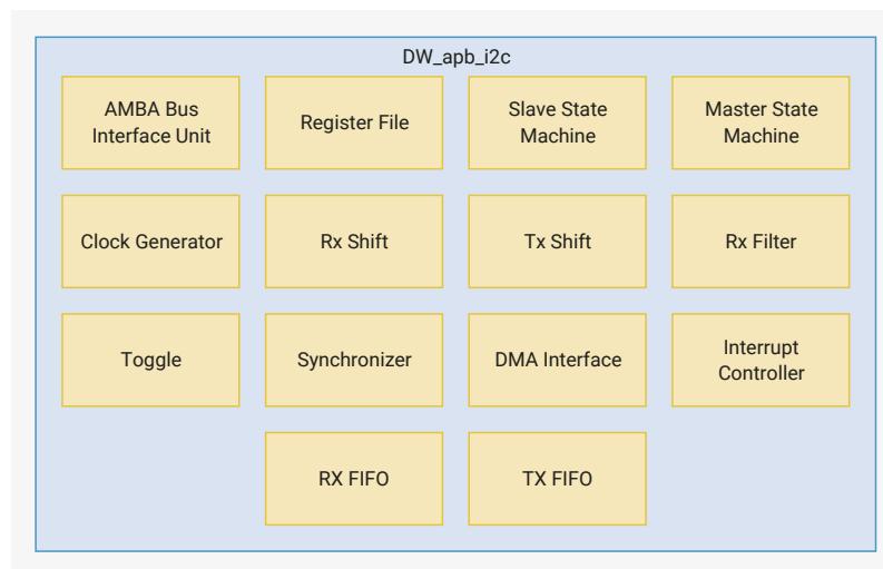
The following define the functions of the blocks in Figure 68 :
- • AMBA Bus Interface Unit: Takes the APB interface signals and translates them into a common generic interface that allows the register file to be bus protocol-agnostic.
- • Register File: Contains configuration registers and is the interface with software.
- • Slave State Machine: Follows the protocol for a slave and monitors bus for address match.
- • Master State Machine: Generates the I2C protocol for the master transfers.
- •
Clock Generator:
Calculates the required timing to do the following:
- ◦ Generate the
SCLclock when configured as a master - ◦ Check for bus idle
- ◦ Generate a START and a STOP
- ◦ Setup the data and hold the data
- ◦ Generate the
- • RX Shift: Takes data into the design and extracts it in byte format.
- • TX Shift: Presents data supplied by CPU for transfer on the I2C bus.
- • RX Filter: Detects the events in the bus; for example, start, stop and arbitration lost.
- • Toggle: Generates pulses on both sides and toggles to transfer signals across clock domains.
- • Synchronizer: Transfers signals from one clock domain to another.
- • DMA Interface: Generates the handshaking signals to the central DMA controller in order to automate the data transfer without CPU intervention.
- • Interrupt Controller: Generates the raw interrupt and interrupt flags, allowing them to be set and cleared.
- • RX FIFO/TX FIFO: Holds the RX FIFO and TX FIFO register banks and controllers, along with their status levels.
12.2.4. I2C terminology
This section defines key terms used in various parts of the I2C.
12.2.4.1. I2C bus terms
The following terms relate to how the role of the I2C device and how it interacts with other I2C devices on the bus.
Transmitter
the device that sends data to the bus. A transmitter can either be a device that initiates the data transmission to the bus (a master-transmitter) or the device that responds to a request from the master to send data to the bus (a slave-transmitter).
Receiver
the device that receives data from the bus. A receiver can either be a device that receives data on its own request (a master-receiver) or a device that receives data in response to a request from the master (a slave-receiver).
Master
the component that initializes a transfer (START command), generates the clock SCL signal and terminates the transfer (STOP command). A master can be either a transmitter or a receiver.
Slave
the device addressed by the master. A slave can be either receiver or transmitter.
Multi-master
the ability for more than one master to co-exist on the bus at the same time without collision or data loss.
Arbitration
the predefined procedure that authorizes only one master at a time to take control of the bus. For more information about this behaviour, refer to Section 12.2.8 .
Synchronization
the predefined procedure that synchronizes the clock signals provided by two or more masters. For more information about this feature, refer to Section 12.2.9 .
SDA
the data signal line (Serial Data).
SCL
the clock signal line (Serial Clock).
12.2.4.2. Bus transfer terms
The following terms are specific to data transfers that occur to and from the I2C bus.
START (RESTART)
data transfer begins with a START or RESTART condition. The level of the SDA data line changes from high to low, while the SCL clock line remains high. When this occurs, the bus becomes busy.
NOTE
START and RESTART conditions are functionally identical.
STOP
data transfer is terminated by a STOP condition. This occurs when the level on the SDA data line passes from the low state to the high state, while the SCL clock line remains high. When the data transfer has been terminated, the bus is free or idle once again. The bus stays busy if a RESTART is generated instead of a STOP condition.
12.2.5. I2C behaviour
The DW_apb_i2c can be controlled with software to be one of the following:
- • An I2C master only, communicating with other I2C slaves
- • An I2C slave only, communicating with one or more I2C masters.
The master is responsible for generating the clock and controlling the transfer of data. The slave is responsible for either transmitting or receiving data to and from the master. The acknowledgement of data is sent by the device that is receiving data, which can be either a master or a slave. As mentioned previously, the I2C protocol also allows multiple masters to reside on the I2C bus and uses an arbitration procedure to determine bus ownership.
Each slave has a unique address determined by the system designer. When a master wants to communicate with a slave:
- 1. The master transmits a START/RESTART condition that is then followed by the slave’s address and a control bit (R/W) to determine if the master wants to transmit data or receive data from the slave.
- 2. The slave then sends an acknowledge (ACK) pulse after the address.
When the master (master-transmitter) writes to the slave (slave-receiver), the receiver gets one byte of data. This transaction continues until the master terminates the transmission with a STOP condition.
When the master reads from a slave (master-receiver), the slave transmits (slave-transmitter) a byte of data to the master. The master then acknowledges the transaction with the ACK pulse. This transaction continues until the master terminates the transmission by not acknowledging (NACK) the transaction after the last byte is received, and then the master issues a STOP condition or addresses another slave after issuing a RESTART condition. This behaviour is illustrated in Figure 69.
Figure 69. Data transfer on the I2C Bus
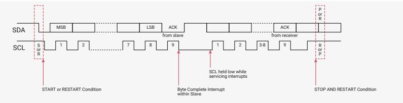
The figure is a timing diagram for an I2C bus transfer. It shows two signals: SDA (Serial Data Arbitration) and SCL (Serial Clock Line). The SDA line is bidirectional, indicated by arrows. The SCL line is unidirectional, indicated by a single arrow. The diagram shows a sequence of operations: 1. START or RESTART Condition: SDA transitions from high to low while SCL is high. 2. Data Transfer: SDA carries data from MSB (Most Significant Bit) to LSB (Least Significant Bit). 3. ACK from slave: SDA transitions from low to high while SCL is high. 4. SCL held low while servicing interrupt: SCL transitions from high to low. 5. Data Transfer: SDA carries data from 1 to 9. 6. ACK from receiver: SDA transitions from low to high while SCL is high. 7. STOP AND RESTART Condition: SDA transitions from low to high while SCL is high. Red dashed boxes highlight the START/RESTART and STOP/RESTART conditions.
The DW_apb_i2c is a synchronous serial interface. The SDA line is a bidirectional signal that changes only while the SCL line is low except for STOP, START, and RESTART conditions. The output drivers are open-drain or open-collector to perform wire-AND functions on the bus. The maximum number of devices on the bus is limited by only the maximum capacitance specification of 400 pF. Data is transmitted in byte packages.
The I2C protocols implemented in DW_apb_i2c are described in more details in Section 12.2.6.
12.2.5.1. START and STOP generation
When operating as an I2C master, putting data into the TX FIFO causes the
DW_apb_i2c
to generate a START condition on the I2C bus. Writing a 1 to
IC_DATA_CMD.STOP
causes the
DW_apb_i2c
to generate a STOP condition on the I2C bus; a STOP condition is not issued if this bit is not set, even if the TX FIFO is empty.
When operating as a slave, the
DW_apb_i2c
does not generate START and STOP conditions, as per the protocol. However, if a read request is made to the
DW_apb_i2c
, it holds the
SCL
line low until read data has been supplied to it. This stalls the I2C bus until read data is provided to the slave
DW_apb_i2c
, or the
DW_apb_i2c
slave is disabled by writing a 0 to
IC_ENABLE.ENABLE
.
12.2.5.2. Combined formats
The
DW_apb_i2c
supports mixed read and write combined format transactions in both 7-bit and 10-bit addressing modes. The
DW_apb_i2c
does not support mixed address and mixed address format - that is, a 7-bit address transaction followed by a 10-bit address transaction or vice versa-combined format transactions. To initiate combined format transfers,
IC_CON.IC_RESTART_EN
should be set to 1. With this value set and operating as a master, when the
DW_apb_i2c
completes an I2C transfer, it checks the TX FIFO and executes the next transfer. If the direction of this transfer differs from the previous transfer, the combined format is used to issue the transfer. If the TX FIFO is empty when the current I2C transfer completes:
- •
IC_DATA_CMD.STOPis checked and:- ◦ If set to 1, a STOP bit is issued.
- ◦ If set to 0, the
SCLis held low until the next command is written to the TX FIFO.
For more details, refer to Section 12.2.7 .
12.2.6. I2C protocols
This section defines protocols used in the
DW_apb_i2c
.
12.2.6.1. START and STOP conditions
When the bus is idle, both the
SCL
and
SDA
signals are pulled high through external pull-up resistors on the bus. When the master wants to start a transmission on the bus, the master issues a
START condition
: a high-to-low transition of the
SDA
signal while
SCL
is 1. When the master wants to terminate the transmission, the master issues a
STOP condition
: a low-to-high transition of the
SDA
signal while
SCL
is 1.
Figure 70
shows the timing of the START and STOP conditions. When data is being transmitted on the bus, the
SDA
signal must be stable when
SCL
is set to 1.
Figure 70. I2C START and STOP Condition
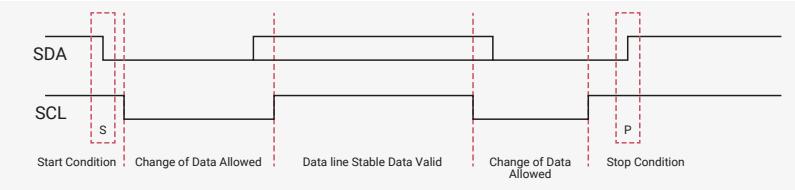
The diagram illustrates the timing of START and STOP conditions on an I2C bus. It shows two signals: SDA (Serial Data Arbitration) and SCL (Serial Clock). The SCL signal is a periodic square wave. The SDA signal is high when the bus is idle and transitions to low during data transmission. The diagram is divided into five regions by vertical dashed lines: 1. Start Condition: SDA transitions from high to low while SCL is high. 2. Change of Data Allowed: SDA is low and SCL is low. 3. Data line Stable Data Valid: SDA is low and SCL is high. 4. Change of Data Allowed: SDA is low and SCL is low. 5. Stop Condition: SDA transitions from low to high while SCL is high. The SDA signal is labeled 'S' at the start and 'P' at the stop.
NOTE
The signal transitions for the START/STOP conditions, as depicted in Figure 70 , reflect those observed at the output signals of the master driving the I2C bus. Care should be taken when observing the SDA/SCL signals at the input signals of slaves, because unequal line delays may result in an incorrect SDA/SCL timing relationship.
12.2.6.2. Addressing slave protocol
There are two address formats: 7-bit and 10-bit.
12.2.6.2.1. 7-bit address format
In the 7-bit address format, the first seven bits (bits 7:1) of the first byte set the slave address and the LSB bit (bit 0) defines the R/W status, as shown in Figure 71 . When bit 0 is set to 0, the master writes to the slave. When bit 0 is set to 1, the master reads from the slave.
Figure 71. I2C 7-bit Address Format
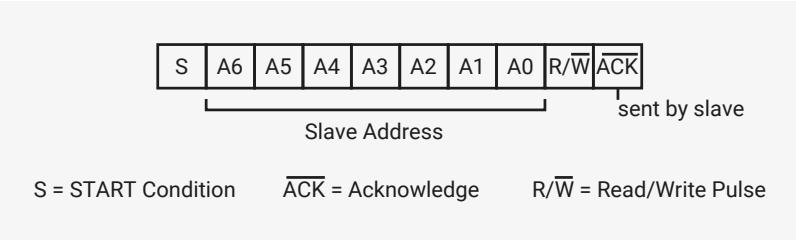
S A6 A5 A4 A3 A2 A1 A0 R/W \( \overline{\text{ACK}} \)
Slave Address sent by slave
S = START Condition \( \overline{\text{ACK}} \) = Acknowledge R/W = Read/Write Pulse
12.2.6.2.2. 10-bit address format
The 10-bit address format transfers two bytes for each 10-bit address.
- • In the first byte, the first five bits (bits 7:3) indicate a 10-bit transfer. The next two bits (bits 2:1) contain bits 9:8 of the slave address. The LSB bit (bit 0) defines the R/W status.
- • The second byte contains bits 7:0 of the slave address.
Figure 72 shows the 10-bit address format:
Figure 72. 10-bit Address Format
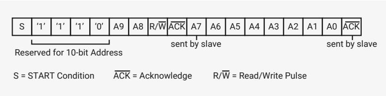
S '1' '1' '1' '0' A9 A8 R/W \( \overline{\text{ACK}} \) A7 A6 A5 A4 A3 A2 A1 A0 \( \overline{\text{ACK}} \)
Reserved for 10-bit Address sent by slave sent by slave
S = START Condition \( \overline{\text{ACK}} \) = Acknowledge R/W = Read/Write Pulse
This table defines the special purpose and reserved first byte addresses.
Table 1051.
I2C/SMBus Definition
of Bits in First Byte
| Slave Address | R/W Bit | Description |
|---|---|---|
| 0000 000 | 0 | General Call Address. DW_apb_i2c places the data in the receive buffer and issues a General Call interrupt. |
| 0000 000 | 1 | START byte. For more details, refer to Section 12.2.6.4 . |
| 0000 001 | X | CBUS address. DW_apb_i2c ignores these accesses. |
| 0000 010 | X | Reserved. |
| Slave Address | R/W Bit | Description |
|---|---|---|
| 0000 011 | X | Reserved. |
| 0000 1XX | X | High-speed master code (for more |
| information, refer to Section 12.2.8 ). | ||
| 1111 1XX | X | Reserved. |
| 1111 0XX | X | 10-bit slave addressing. |
| 0001 000 | X | SMbus Host. (not supported) |
| 0001 100 | X | SMBus Alert Response Address. (not supported) |
| 1100 001 | X | SMBus Device Default Address. (not supported) |
| issuing a STOP condition. The slave must leave the | SDA | line high so that the master can abort the transfer. If the master- |
| transmitter is transmitting data as shown in acknowledge pulse after every byte of data is received. | Figure 73 | , the slave-receiver responds to the master-transmitter with an |
| For 7-bit Address Transmitter Protocol S Slave Address R/W A ‘0’ (read) | DATA A DAT A A/A P | |
| For 10-bit Address S Slave Address First 7 bits R/W A ‘11110xxx’ ‘0’ (write) | Slave Address Second Byte A DATA A/A P | |
| From Master to Slave | A = Acknowledge (SDA low) S = START Condition | |
| From Slave to Master | A = No Acknowledge (SDA high) P = STOP Condition | |
| 12.2.6.3.2. Master-receiver and slave-transmitter If the master is receiving data as shown i | n Figure 74 | the master responds to the slave-transmitter with an acknowledge |
| transmitter that this is the last byte. The slave-transmitter relinquishes the | SDA line after detecting No Acknowledge |
DW_apb_i2c
does not restrict you from using reserved addresses. However, if you use these reserved addresses, you may experience incompatibilities with I2C components.
12.2.6.3. Transmitting and receiving protocol
The master can initiate data transmission and reception to and from the bus, acting as either a master-transmitter or master-receiver. A slave responds to requests from the master to either transmit data or receive data to/from the bus, acting as either a slave-transmitter or slave-receiver, respectively.
12.2.6.3.1. Master-transmitter and slave-receiver
All data is transmitted in byte format, with no limit on the number of bytes transferred per data transfer. After the master sends the address and R/W bit or the master transmits a byte of data to the slave, the slave-receiver must respond with the acknowledge signal (ACK). When no slave-receiver responds with an ACK pulse, the master aborts the transfer by issuing a STOP condition. The slave must leave the SDA line high so that the master can abort the transfer. If the master-transmitter is transmitting data as shown in Figure 73 , the slave-receiver responds to the master-transmitter with an acknowledge pulse after every byte of data is received.
Figure 73. I2C Master-Transmitter Protocol
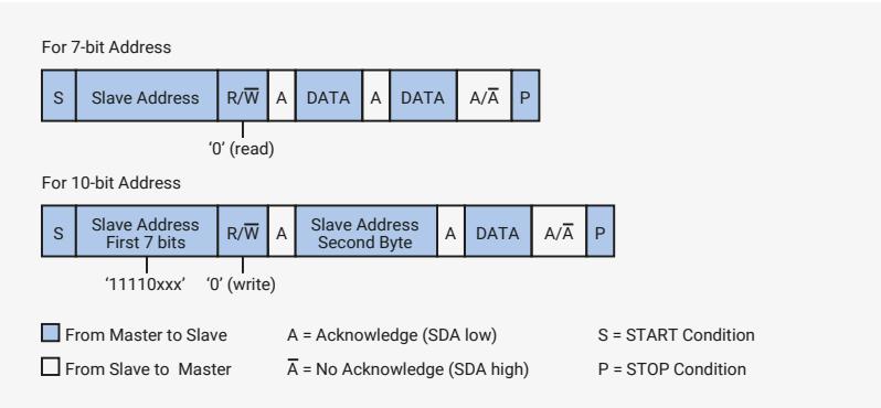
The diagram illustrates the I2C Master-Transmitter Protocol for two address types: 7-bit and 10-bit.
For 7-bit Address: The sequence of bytes is S (START), Slave Address (7 bits), R/W bit (0 for read), A (Acknowledge), DATA, A (Acknowledge), DATA, A/A̅ (Acknowledge/No Acknowledge), and P (STOP). A label '0' (read)' points to the R/W bit.
For 10-bit Address: The sequence of bytes is S (START), Slave Address First 7 bits, R/W bit (0 for write), A (Acknowledge), Slave Address Second Byte, A (Acknowledge), DATA, A/A̅ (Acknowledge/No Acknowledge), and P (STOP). A label '11110xxx' '0' (write)' points to the R/W bit.
Legend:
- Blue box: From Master to Slave
- White box: From Slave to Master
- A = Acknowledge (SDA low)
- A̅ = No Acknowledge (SDA high)
- S = START Condition
- P = STOP Condition
12.2.6.3.2. Master-receiver and slave-transmitter
If the master is receiving data as shown in Figure 74 the master responds to the slave-transmitter with an acknowledge pulse after receiving each byte of data, except for the last byte. This is the way the master-receiver notifies the slave-transmitter that this is the last byte. The slave-transmitter relinquishes the SDA line after detecting No Acknowledge (NACK) so that the master can issue a STOP condition.
Figure 74. I2C Master-Receiver Protocol
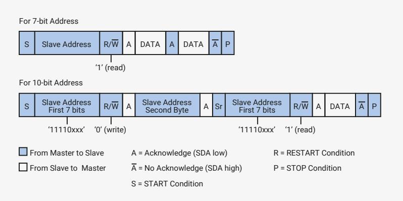
The diagram illustrates the I2C Master-Receiver Protocol for two address formats: 7-bit and 10-bit.
For 7-bit Address:
- Sequence: S (Start) → Slave Address (7 bits) → R/W (Read/Write) → A (Acknowledge) → DATA → A (Acknowledge) → \( \bar{A} \) (No Acknowledge) → P (Stop).
- Direction: Slave Address and DATA are transmitted from Master to Slave. R/W, A, and \( \bar{A} \) are signals on the bus.
- Read/Write: R/W = '1' (read) for the 7-bit address format.
For 10-bit Address:
- Sequence: S (Start) → Slave Address First 7 bits → R/W (Read/Write) → A (Acknowledge) → Slave Address Second Byte → A (Acknowledge) → Sr (Restart) → Slave Address First 7 bits → R/W (Read/Write) → A (Acknowledge) → DATA → \( \bar{A} \) (No Acknowledge) → P (Stop).
- Direction: Slave Address First 7 bits, Slave Address Second Byte, and DATA are transmitted from Master to Slave. R/W, A, and \( \bar{A} \) are signals on the bus.
- Read/Write: R/W = '0' (write) for the first 7 bits and '1' (read) for the second 7 bits.
Legend:
- Blue box: From Master to Slave
- White box: From Slave to Master
- A = Acknowledge (SDA low)
- \( \bar{A} \) = No Acknowledge (SDA high)
- S = START Condition
- R = RESTART Condition
- P = STOP Condition
When a master does not want to relinquish the bus with a STOP condition, the master can issue a RESTART condition. This is identical to a START condition except it occurs after the ACK pulse. Operating in master mode, the
DW_apb_i2c
can then communicate with the same slave using a transfer of a different direction. For a description of the combined format transactions that the
DW_apb_i2c
supports, see
Section 12.2.5.2
.
NOTE
The
DW_apb_i2c
must be completely disabled before the target slave address register (
IC_TAR
) can be reprogrammed.
12.2.6.4. START BYTE Transfer Protocol
The START BYTE transfer protocol is designed for systems that do not have an on-board dedicated I2C hardware module. When the
DW_apb_i2c
is addressed as a slave, it always samples the I2C bus at the highest speed supported so that it never requires a START BYTE transfer. However, when
DW_apb_i2c
is a master, it supports the generation of START BYTE transfers at the beginning of every transfer in case a slave device requires it.
This protocol consists of the transmission of seven zeros, followed by a one, as illustrated in Figure 75 . This allows the processor polling the bus to under-sample the address phase until zero is detected. Once the microcontroller detects a zero, it switches from the under sampling rate to the correct rate of the master.
Figure 75. I2C Start Byte Transfer
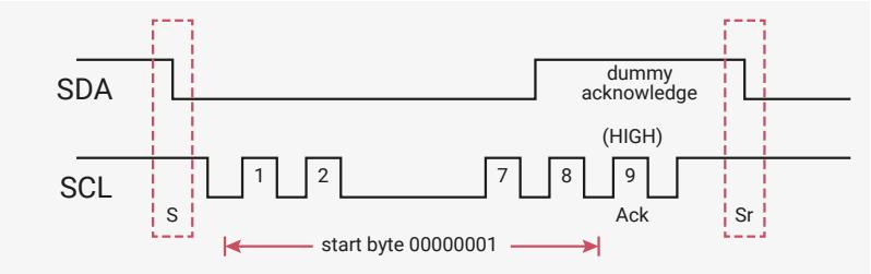
The diagram shows the timing of the I2C Start Byte Transfer. The SDA (Serial Data) line is pulled up to a high state. The SCL (Serial Clock) line is shown with a series of pulses. The start byte is transmitted as a sequence of seven zeros followed by a one (00000001). The SCL line is labeled with 'S' for the start condition, '1' for the first bit, '2' for the second bit, '7' for the seventh bit, '8' for the eighth bit, '9' for the ninth bit, and 'Ack' for the acknowledgment pulse. The SDA line is labeled with 'dummy acknowledge (HIGH)' during the acknowledgment phase. The SCL line is labeled with 'Sr' for the restart condition. A red dashed box highlights the start byte sequence on the SCL line.
The START BYTE procedure is as follows:
- 1. Master generates a START condition.
- 2. Master transmits the START byte (0000 0001).
- 3. Master transmits the ACK clock pulse. (Present only to conform with the byte handling format used on the bus)
- 4. No slave sets the ACK signal to zero.
- 5. Master generates a RESTART (R) condition.
Hardware receivers do not respond to the START BYTE procedure because it uses a reserved address and resets after the RESTART condition generates.
12.2.7. TX FIFO Management and START, STOP and RESTART Generation
When operating as a master, the
DW_apb_i2c
component supports the mode of TX (transmit) FIFO management illustrated in Figure 76.
12.2.7.1. TX FIFO management
The component does not generate a STOP if the TX FIFO becomes empty; in this situation the component holds the
SCL
line low, stalling the bus until a new entry is available in the TX FIFO. A STOP condition is generated only when the user specifically requests it by setting bit nine (Stop bit) of the command written to
IC_DATA_CMD
register. Figure 76 shows the bits in the
IC_DATA_CMD
register.
Figure 76.IC_DATA_CMD
Register
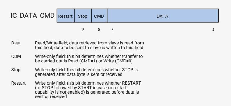
The diagram shows the
IC_DATA_CMD
register structure. It is a 10-bit register with the following fields:
- Restart : Bit 9. Write-only field; this bit determines whether RESTART (or STOP followed by START in case or restart capability is not enabled) is generated before data is sent or received.
- Stop : Bit 8. Write-only field; this bit determines whether STOP is generated after data byte is sent or received.
- CMD : Bit 7. Write-only field; this bit determines whether transfer to be carried out is Read (CMD=1) or Write (CMD=0).
- DATA : Bits 6-0. Read/Write field; data retrieved from slave is read from this field; data to be sent to slave is written to this field.
Figure 77 illustrates the behaviour of the
DW_apb_i2c
when the TX FIFO becomes empty while operating as a master transmitter, as well as the generation of a STOP condition.
Figure 77. Master
Transmitter - TX FIFO
Empties/STOP
Generation
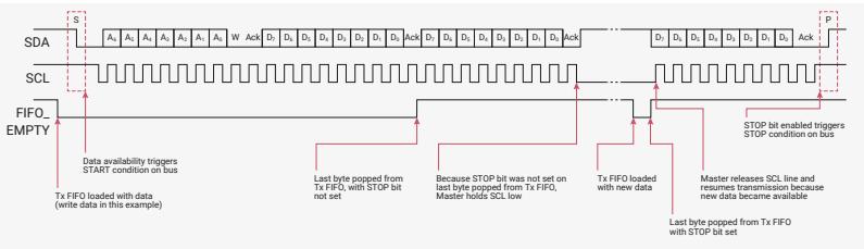
The diagram shows the SDA and SCL lines over time. It illustrates the sequence of events when the TX FIFO becomes empty during a master transmitter operation. Key events include:
- SDA line starts with a START condition (S).
- Data is written to the TX FIFO (Tx FIFO loaded with data).
- Data is transferred from the TX FIFO to the SDA line (Data availability triggers START condition on bus).
- The TX FIFO becomes empty (FIFO EMPTY).
- The last byte is popped from the TX FIFO with the STOP bit not set.
- Because the STOP bit was not set on the last command popped from the TX FIFO, the Master holds the SCL line low.
- The TX FIFO is loaded with new data.
- The Master releases the SCL line and resumes transmission because new data became available.
- The last byte is popped from the TX FIFO with the STOP bit set.
- The STOP bit enabled triggers a STOP condition on the bus.
Figure 78 illustrates the behaviour of the
DW_apb_i2c
when the TX FIFO becomes empty while operating as a master receiver, as well as the generation of a STOP condition.
Figure 78. Master
Receiver - TX FIFO
Empties/STOP
Generation
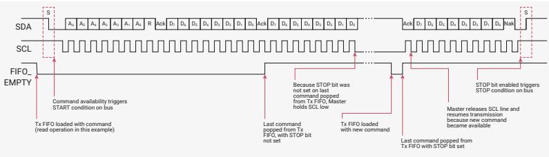
The diagram shows the SDA and SCL lines over time. It illustrates the sequence of events when the TX FIFO becomes empty during a master receiver operation. Key events include:
- SDA line starts with a START condition (S).
- A command is written to the TX FIFO (Tx FIFO loaded with command).
- The command is transferred from the TX FIFO to the SDA line (Command availability triggers START condition on bus).
- The TX FIFO becomes empty (FIFO EMPTY).
- The last command is popped from the TX FIFO with the STOP bit not set.
- Because the STOP bit was not set on the last command popped from the TX FIFO, the Master holds the SCL line low.
- The TX FIFO is loaded with new command.
- The Master releases the SCL line and resumes transmission because new command became available.
- The last command is popped from the TX FIFO with the STOP bit set.
- The STOP bit enabled triggers a STOP condition on the bus.
Figure 79 and Figure 80 illustrate configurations where the user can control the generation of RESTART conditions on the I2C bus. If bit 10 (Restart) of the
IC_DATA_CMD
register is set and the restart capability is enabled (
IC_RESTART_EN=1
), a RESTART is generated before the data byte is written to or read from the slave. If the restart capability is not enabled, a STOP followed by a START is generated in place of the RESTART. Figure 79 illustrates this situation during operation as a master transmitter.
Figure 79. Master Transmitter - Restart Bit of
IC_DATA_CMD
Is Set
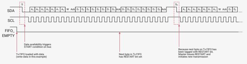
Figure 84. Master Receiver - First Command Loaded After TX FIFO Allowed to Empty/Restart Bit Set
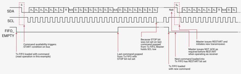
The diagram shows the interaction between the SDA and SCL lines and the TX FIFO. Key events include: a START condition on SDA; the TX FIFO being loaded with a command; the master popping the command from the FIFO; the master holding SCL low; the master issuing a RESTART; and the master issuing a NOT ACK as required before the RESTART. The TX FIFO is then loaded with a new command.
12.2.8. Multiple master arbitration
The
DW_apb_i2c
bus protocol allows multiple masters to reside on the same bus. If there are two masters on the same I2C bus, there is an arbitration procedure if both try to take control of the bus at the same time by generating a START condition at the same time. Once a master (for example, a microcontroller) has control of the bus, no other master can take control until the first master sends a STOP condition and places the bus in an idle state.
Arbitration takes place on the
SDA
line, while the
SCL
line is set to 1. The master, which transmits a one while the other master transmits zero, loses arbitration and turns off its data output stage. The master that lost arbitration can continue to generate clocks until the end of the byte transfer. If both masters address the same slave device, the arbitration could go into the data phase.
Upon detecting that it has lost arbitration to another master, the
DW_apb_i2c
stops generating
SCL
by disabling the output driver. Figure 85 illustrates the timing of two masters arbitrating on the bus.
Figure 85. Multiple Master Arbitration
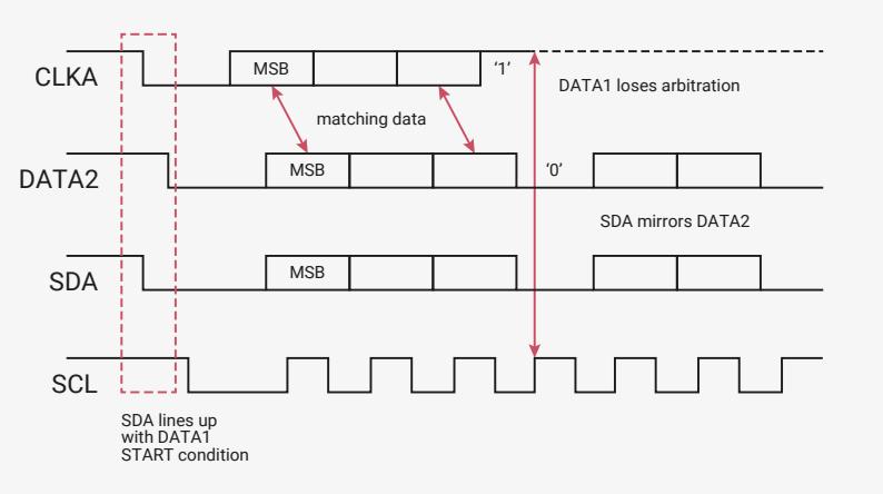
The diagram shows the arbitration process between two masters. It includes signals for CLK_A, DATA2, SDA, and SCL. Key events include: SDA lines up with DATA1 START condition; matching data; DATA1 loses arbitration; SDA mirrors DATA2; and SCL is set to 1.
Control of the bus is determined by address or master code and data sent by competing masters, so there is no central master nor any order of priority on the bus.
Arbitration is not allowed between the following conditions:
- • A RESTART condition and a data bit
- • A STOP condition and a data bit
- • A RESTART condition and a STOP condition
i NOTE
Slaves do not participate in the arbitration process.
12.2.9. Clock synchronisation
When two or more masters try to transfer information on the bus at the same time, they must arbitrate and synchronize the
SCL
clock. All masters generate their own clock to transfer messages. Data is valid only during the high period of
SCL
.
clock. Clock synchronisation is performed using the wired-AND connection to the SCL signal. When the master transitions the SCL clock to zero, the master starts counting the low time of the SCL clock and transitions the SCL clock signal to one at the beginning of the next clock period. However, if another master is holding the SCL line to 0, then the master goes into a HIGH wait state until the SCL clock line transitions to one.
All masters then count off their high time, and the master with the shortest high time transitions the SCL line to zero. The masters then count out their low time and the one with the longest low time forces the other masters into a HIGH wait state. Therefore, a synchronized SCL clock is generated, which is illustrated in Figure 86. Optionally, slaves may hold the SCL line low to slow down the timing on the I2C bus.
Figure 86. Multi-Master Clock Synchronisation
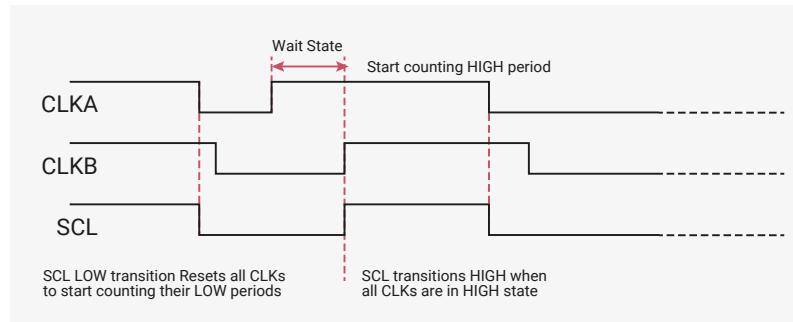
The diagram illustrates the clock synchronisation process on an I2C bus. It shows three signals: CLK_A, CLK_B, and SCL. CLK_A and CLK_B represent the individual clock signals from two different masters. SCL is the resulting synchronized clock signal. The process starts with SCL being low. When SCL transitions low, it resets all CLKs to start counting their LOW periods. As CLK_A and CLK_B transition high, SCL remains low. When CLK_A transitions low, SCL transitions high, starting the counting of the HIGH period. If CLK_B transitions low while SCL is high, SCL remains high, forcing CLK_B into a HIGH wait state. This process repeats until all masters have completed their high time, and SCL transitions low again, forcing all masters into a LOW wait state. The diagram includes labels for 'Wait State' and 'Start counting HIGH period'.
12.2.10. Operation modes
This section provides information about operation modes.
i NOTE
Only set the DW_apb_i2c to operate as an I2C Master or an I2C Slave. Never set the DW_apb_i2c to operate as both simultaneously. To avoid this, never simultaneously set IC_CON.IC_SLAVE_DISABLE and IC_CON.MASTER_MODE to zero and one, respectively.
12.2.10.1. Slave mode operation
This section discusses slave mode procedures.
12.2.10.1.1. Initial configuration
To use the DW_apb_i2c as a slave, perform the following steps:
- 1. Disable the DW_apb_i2c by writing a 0 to IC_ENABLE.ENABLE .
- 2. Write to the IC_SAR register (bits 9:0) to set the slave address. This is the address to which the DW_apb_i2c responds.
- 3. Write to the IC_CON register to specify which type of addressing is supported (7-bit or 10-bit by setting bit 3). Enable the DW_apb_i2c in slave-only mode by writing a 0 into bit six ( IC_CON.IC_SLAVE_DISABLE ) and a 0 to bit zero ( IC_CON.MASTER_MODE ).
Slaves and masters can use different addressing settings. For instance, a slave can be programmed with 7-bit addressing and a master with 10-bit addressing, and vice versa.
- 4. Enable the
DW_apb_i2cby writing a 1 toIC_ENABLE.ENABLE.
Depending on the reset values chosen, steps two and three may not be necessary because the reset values can be configured. For instance, if the device is only going to be a master, there would be no need to set the slave address because you can configure
DW_apb_i2c
to have the slave disabled after reset and to enable the master after reset. The values stored are static and do not need to be reprogrammed if the
DW_apb_i2c
is disabled.
Only bring the
DW_apb_i2c
Slave out of reset when the I2C bus is IDLE. De-asserting the reset when a transfer is ongoing on the bus causes internal synchronization flip-flops used to synchronize
SDA
and
SCL
to toggle from a reset value of one to the actual value on the bus. This can result in
SDA
toggling from one to zero while
SCL
is one, thereby causing a false START condition to be detected by the
DW_apb_i2c
Slave. This scenario can also be avoided by configuring the
DW_apb_i2c
with
IC_SLAVE_DISABLE = 1
and
MASTER_MODE = 1
so that the Slave interface is disabled after reset. It can then be enabled by programming
IC_CON[0] = 0
and
IC_CON[6] = 0
after the internal
SDA
and
SCL
have synchronized to the value on the bus; this takes approximately six
ic_clk
cycles after reset de-assertion.
When another I2C master device on the bus addresses the
DW_apb_i2c
and requests data, the
DW_apb_i2c
acts as a slave-transmitter. The following steps occur:
- 1. The other I2C master device initiates an I2C transfer with an address that matches the slave address in the
IC_SARregister of theDW_apb_i2c. - 2. The
DW_apb_i2cacknowledges the sent address and recognizes the direction of the transfer to indicate that it is acting as a slave-transmitter. - 3. The
DW_apb_i2casserts theRD_REQinterrupt (bit five of theIC_RAW_INTR_STATregister) and holds theSCLline low. It remains in a wait state until software responds. If theRD_REQinterrupt has been masked, due toIC_INTR_MASK.M_RD_REQbeing set to zero, use a hardware and/or software timing routine to instruct the CPU to perform periodic reads of theIC_RAW_INTR_STATregister.- ◦ Reads that indicate
IC_RAW_INTR_STAT.RD_REQbeing set to one must be treated as the equivalent of theRD_REQinterrupt being asserted. - ◦ Software must then act to satisfy the I2C transfer.
- ◦ The timing interval used should be in the order of 10 times the fastest
SCLclock period theDW_apb_i2ccan handle. For example, for 400 kb/s, the timing interval is 25µs.
- ◦ Reads that indicate
The value of 10 is recommended here because this is approximately the amount of time required for a single byte of data transferred on the I2C bus.
- 4. If there is any data remaining in the TX FIFO before receiving the read request, the
DW_apb_i2casserts aTX_ABRTinterrupt (bit six of theIC_RAW_INTR_STATregister) to flush the old data from the TX FIFO. If theTX_ABRTinterrupt has been masked, due toIC_INTR_MASK.M_TX_ABRTbeing set to zero, re-use the timing routine described in the previous step to read theIC_RAW_INTR_STATregister.
Because the
DW_apb_i2c
's TX FIFO is forced into a flushed/reset state whenever a
TX_ABORT
event occurs, software must release the
DW_apb_i2c
from this state by reading the
IC_CLR_TX_ABORT
register before attempting to write into the TX FIFO. See register
IC_RAW_INTR_STAT
for more details.
- ◦ Reads that indicate bit six (
R_TX_ABORT) being set to one must be treated as the equivalent of theTX_ABORTinterrupt being asserted. - ◦ There is no further action required from software.
- ◦ The timing interval used should be similar to that described in the previous step for the
IC_RAW_INTR_STAT.RD_REQregister.
- ◦ Reads that indicate bit six (
- 5. Software writes to the
IC_DATA_CMDregister with the data to be written (by writing a 0 in bit 8). - 6. Software must clear the
RD_REQandTX_ABORTinterrupts (bits five and six, respectively) of theIC_RAW_INTR_STATregister before proceeding. If theRD_REQorTX_ABORTinterrupts have been masked, then clearing of theIC_RAW_INTR_STATregister will have already been performed when either theR_RD_REQorR_TX_ABORTbit has been read as one. - 7. The
DW_apb_i2creleases theSCLand transmits the byte. - 8. The master may hold the I2C bus by issuing a RESTART condition or release the bus by issuing a STOP condition.
- 5. Software writes to the
Slave-Transmitter Operation for a single byte is not applicable in Ultra-Fast mode, since this mode does not support read transfers.
12.2.10.1.3. Slave-receiver operation for a single byteWhen another I2C master device on the bus addresses the
DW_apb_i2c
and is sending data, the
DW_apb_i2c
acts as a slave-receiver and the following steps occur:
- 1. The other I2C master device initiates an I2C transfer with an address that matches the
DW_apb_i2c's slave address in theIC_SARregister. - 2. The
DW_apb_i2cacknowledges the sent address and recognizes the direction of the transfer to indicate that theDW_apb_i2cis acting as a slave-receiver. - 3.
DW_apb_i2creceives the transmitted byte and places it in the receive buffer.
If the Rx (receive) FIFO is completely filled with data when a byte is pushed, then the
DW_apb_i2c
slave holds the I2C
SCL
line low until the Rx FIFO has some space, and then continues with the next read request.
- 4.
DW_apb_i2casserts theRX_FULLinterruptIC_RAW_INTR_STAT.RX_FULL. If theRX_FULLinterrupt has been masked, due to settingIC_INTR_MASK.M_RX_FULLto zero or settingIC_TX_TLto a value larger than zero, you should implement a timing routine (described in Section 12.2.10.1.2) for periodic reads of theIC_STATUSregister. This timing routine should treat reads of theIC_STATUSregister, with bit 3 (RFNE) set at one as the equivalent of anRX_FULLinterrupt. - 5. Software may read the byte from the
IC_DATA_CMDregister (bits 7:0). - 6. The other master device may hold the I2C bus by issuing a RESTART condition, or release the bus by issuing a STOP condition.
12.2.10.1.4. Slave-transfer operation for bulk transfers
In the standard I2C protocol, all transactions are single byte transactions; the programmer responds to a remote master read request by writing one byte into the slave's TX FIFO. When a slave (slave-transmitter) receives a read request ( RD_REQ ) from the remote master (master-receiver), at a minimum there should be at least one entry placed into the slave-transmitter's TX FIFO.
DW_apb_i2c handles more data in the TX FIFO. This enables subsequent read requests to take data without raising an interrupt. This eliminates latencies incurred between interrupts. This mode only occurs when DW_apb_i2c acts as a slave-transmitter. If the remote master acknowledges the data sent by the slave-transmitter and there is no data in the slave's TX FIFO, the DW_apb_i2c holds the I2C SCL line low while it raises the read request interrupt ( RD_REQ ) and waits for a data write into the TX FIFO.
If the RD_REQ interrupt is masked by setting IC_INTR_STAT.R_RD_REQ to zero, use a timing routine to activate periodic reads of the IC_RAW_INTR_STAT register. Reads of IC_RAW_INTR_STAT that return bit five ( RD_REQ ) set to one must be treated as the equivalent of RD_REQ . This timing routine is similar to that described in Section 12.2.10.1.2 .
The RD_REQ interrupt is raised upon a read request. Always clear this interrupt when exiting the interrupt service handling routine (ISR). The ISR allows you to either write one byte or more than one byte into the TX FIFO. The master can request additional data at the end of a transmission by acknowledging the last byte. In this scenario, the slave must raise RD_REQ again.
If you know in advance that the remote master requests a packet of n bytes, you can write n byte to the TX FIFO. Then, when another master addresses DW_apb_i2c and requests data, the remote master will receive a continuous stream of data. This happens because the DW_apb_i2c slave continues to send data to the remote master as long as the remote master acknowledges the data sent and there is data available in the TX FIFO. There is no need to hold the SCL line low or to issue RD_REQ again.
If the remote master doesn't read all of the bytes from the TX FIFO, the DW_apb_i2c ignores the excess bytes with the following procedure:
- • The DW_apb_i2c clears the TX FIFO.
- • The DW_apb_i2c generates a transmit abort ( TX_ABORT ) event.
At the time an ACK/NACK is expected, if a NACK is received, then the remote master has all the data it wants. At this time, a flag is raised within the slave's state machine to clear the leftover data in the TX FIFO. This flag is transferred to the processor bus clock domain where the FIFO exists and the contents of the TX FIFO is cleared at that time.
12.2.10.2. Master mode operation
This section discusses master mode procedures.
12.2.10.2.1. Initial configuration
To use the DW_apb_i2c as a master, perform the following steps:
- 1. Disable the DW_apb_i2c by writing zero to IC_ENABLE.ENABLE .
- 2. Write to the IC_CON register to set the maximum speed mode supported (bits 2:1) and the desired speed of the DW_apb_i2c master-initiated transfers, either 7-bit or 10-bit addressing (bit 4). Ensure that bit six ( IC_SLAVE_DISABLE ) is written with a 1 and bit zero ( MASTER_MODE ) is written with a 1.
Slaves and masters can use different addressing settings. For instance, a slave can be programmed with 7-bit addressing and a master with 10-bit addressing, and vice versa.
- 3. Write the address of the I2C device to be addressed to bits 9:0 of the IC_TAR register. This register also determines whether the I2C will perform a General Call or a START BYTE command.
- 4. Enable the DW_apb_i2c by writing a one to IC_ENABLE.ENABLE .
- 5. Write the transfer direction and the data to be sent to the IC_DATA_CMD register. This step generates the START condition and the address byte on the DW_apb_i2c . Once DW_apb_i2c is enabled and there is data in the TX FIFO, DW_apb_i2c starts reading the data.
If you write to the IC_DATA_CMD register before enabling the DW_apb_i2c , the data and commands are lost: the buffers are kept cleared when DW_apb_i2c is disabled.
The values stored are static and do not need to be reprogrammed when the DW_apb_i2c is disabled except for transfer direction and data. As a result, you may not need to perform steps two, three, four, and five if you already configured the reset values.
12.2.10.2.2. Master transmit and master receiveThe DW_apb_i2c supports switching back and forth between reading and writing dynamically. To transmit data, write data to the lower byte of the I2C RX/TX Data Buffer and Command Register ( IC_DATA_CMD ). For I2C write operations, write zero to the CMD bit [8]. Subsequently, to issue a read command, write a one to the CMD bit and write don't care to the lower byte of the IC_DATA_CMD register. The DW_apb_i2c master continues to initiate transfers as long as there are commands present in the TX FIFO. If the TX FIFO becomes empty, the master performs one of the following actions based on the value of IC_DATA_CMD :
- • If set to one, it issues a STOP condition after completing the current transfer.
- • If set to zero, it holds SCL low until next command is written to the TX FIFO.
For more details, refer to Section 12.2.7 .
12.2.10.3. Disabling DW_apb_i2cThe IC_ENABLE_STATUS register allows software to unambiguously determine when the I2C hardware has completely shut down.
NOTEEarlier versions of DW_apb_i2c required the programmer to monitor two registers: ( IC_STATUS and IC_RAW_INTR_STAT ). RP2350 only requires the programmer to monitor IC_ENABLE_STATUS .
To shut down I2C hardware, write a zero to IC_ENABLE.ENABLE . The DW_apb_i2c master can be disabled only if the command currently processing when the de-assertion occurs has the STOP bit set to one. If you attempt to disable the DW_apb_i2c master while processing a command without the STOP bit set, the DW_apb_i2c master continues to remain active, holding the SCL line low until a new command is received in the TX FIFO.
To relinquish the I2C bus and disable DW_apb_i2c while the DW_apb_i2c master is processing a command without the STOP bit set, issue an ABORT request .
12.2.10.3.1. Procedure
- 1. Define a timer interval (
\(
t_{i2c\_poll}
\)
) equal to the 10 times the signalling period for the highest I2C transfer speed used in the system and supported by
DW_apb_i2c. For example, if the highest I2C transfer mode is 400 kb/s, \( t_{i2c\_poll} \) is 25µs. - 2. Define a maximum time-out parameter,
MAX_T_POLL_COUNT, such that if any repeated polling operation exceeds this maximum value, an error is reported. - 3. Execute a blocking thread, process, or function that prevents any further I2C master transactions from starting from software, but allows any pending transfers to be completed.
i NOTE
This step can be ignored if
DW_apb_i2c
is programmed to operate as an I2C slave only.
- 1. The variable
POLL_COUNTis initialized to zero. - 2. Set bit zero of the
IC_ENABLEregister to zero. - 3. Read the
IC_ENABLE_STATUSregister and test theIC_ENbit (bit 0). IncrementPOLL_COUNTby one. IfPOLL_COUNT >= MAX_T_POLL_COUNT, exit with the relevant error code. - 4. If
IC_ENABLE_STATUS[0]is one, sleep for \( t_{i2c\_poll} \) and proceed to the previous step. Otherwise, exit with a relevant success code.
12.2.10.4. Aborting I2C transfers
The
ABORT
control bit of the
IC_ENABLE
register allows the software to relinquish the I2C bus before completing the issued transfer commands from the TX FIFO. In response to an
ABORT
request, the controller issues the STOP condition over the I2C bus, followed by a TX FIFO flush. Aborting the transfer is allowed only in master mode of operation.
12.2.10.4.1. Procedure
- 1. Stop filling the TX FIFO (
IC_DATA_CMD) with new commands. - 2. When operating in DMA mode, disable the transmit DMA by setting
TDMAEto zero. - 3. Set
IC_ENABLE.ABORTto one. - 4. Wait for the
M_TX_ABRTinterrupt. - 5. Read the
IC_TX_ABRT_SOURCEregister to identify the source asABRT_USER_ABRT.
12.2.11. Spike suppression
The
DW_apb_i2c
contains programmable spike suppression logic that matches requirements imposed by the I2C Bus Specification for SS/FS modes. This logic is based on counters that monitor the input signals (
SCL
and
SDA
), checking if they remain stable for a predetermined amount of
ic_clk
cycles before they are sampled internally. There is one separate counter for each signal (
SCL
and
SDA
). The number of
ic_clk
cycles can be programmed by the user. The value should account for the frequency of
ic_clk
and the relevant spike length specification. Each counter starts whenever its input signal changes value. Depending on the behaviour of the input signal, one of the following scenarios occurs:
- • The input signal remains unchanged until the counter reaches its count limit value. When this happens, the counter resets and stops, and the internal version of the signal updates to the input value.
- • The input signal changes again before the counter reaches its count limit value. When this happens, the counter resets and stops, but the internal version of the signal does not update.
The timing diagram in Figure 87 illustrates the behaviour described above.
Figure 87. Spike
Suppression Example
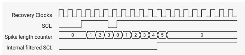
The diagram illustrates the spike suppression logic. The Recovery Clocks are shown as a regular square wave. The SCL signal is a square wave that transitions from high to low, then back to high, and then to low again. The Spike length counter is a sequence of values: 0, 1, 2, 3, 0, 1, 2, 3, 4, 5, 0. The Internal filtered SCL is a square wave that is low during the spike and returns to high after the counter reaches 5.
NOTE
There is a 2-stage synchronizer on the SCL input. For the sake of simplicity, this synchronization delay was not included in the timing diagram in Figure 87 .
The I2C Bus Specification calls for different maximum spike lengths according to the operating mode (50 ns for SS and FS). Register IC_FS_SPKLEN holds the maximum spike length for SS and FS modes.
This register is 8 bits wide and accessible through the APB interface for reads and writes. However, you can only write to this register when the DW_apb_i2c is disabled. The minimum value that can be programmed into these registers is one; attempting to program a value smaller than one results in the value one being written.
The default value for these registers is based on the value of 100 ns for ic_clk period, so should be updated for the clk_sys period in use on RP2350.
NOTE
- • Because the minimum value that can be programmed into the IC_FS_SPKLEN register is one, the spike length specification can be exceeded for low frequencies of ic_clk . Consider the simple example of a 10 MHz (100 ns period) ic_clk ; in this case, the minimum spike length that can be programmed is 100 ns, which means that spikes up to this length are suppressed.
- • Standard synchronization logic (two flip-flops in series) is implemented upstream of the spike suppression logic and is not affected in any way by the contents of the spike length registers or the operation of the spike suppression logic; the two operations (synchronization and spike suppression) are completely independent. Because the SCL and SDA inputs are asynchronous to ic_clk , there is one ic_clk cycle uncertainty in the sampling of these signals. Depending on when they occur relative to the rising edge of ic_clk , spikes of the same original length might show a difference of one ic_clk cycle after being sampled.
- • Spike suppression is symmetrical; the behaviour is exactly the same for transitions from zero to one and from one to zero.
12.2.12. Fast mode plus operation
In fast mode plus, the DW_apb_i2c extends fast mode operation to be support speeds up to 1000 kb/s. To enable the DW_apb_i2c for fast mode plus operation, perform the following steps before initiating any data transfer:
- 1. Set ic_clk frequency greater than or equal to 32 MHz (refer to Section 12.2.14.2.1 ).
- 2. Program the IC_CON register [2:1] = 2'b10 for fast mode or fast mode plus.
- 3. Program IC_FS_SCL_LCNT and IC_FS_SCL_HCNT registers to meet the fast mode plus SCL (refer to Section 12.2.14 ).
- 4. Program the IC_FS_SPKLEN register to suppress the maximum spike of 50 ns.
- 5. Program the IC_SDA_SETUP register to meet the minimum data setup time (tSU; DAT).
12.2.13. Bus clear feature
DW_apb_i2c supports the bus clear feature that provides graceful recovery of data SDA and clock SCL lines during unlikely events in which either the clock or data line is stuck at LOW.
12.2.13.1. SDA line is stuck at LOW
In case of SDA line stuck at LOW, the master performs the following actions to recover as shown in Figure 88 and Figure 89:
- 1. Master sends a maximum of nine clock pulses to recover the bus LOW within those nine clocks.
- ◦ The number of clock pulses will vary with the number of bits that remain to be sent by the slave. As the maximum number of bits is nine, master sends up to nine clock pluses and allows the slave to recover.
- ◦ The master attempts to assert a Logic 1 on the SDA line and check whether SDA is recovered. If the SDA is not recovered, it will continue to send a maximum of nine SCL clocks.
- 2. If SDA line is recovered within nine clock pulses, the master will send STOP to release the bus.
- 3. If SDA line is not recovered even after the ninth clock pulse, you must hardware reset the system.
Figure 88. SDA Recovery with 9 SCL Clocks
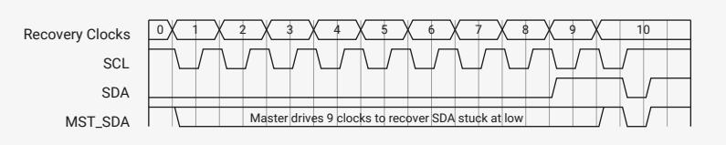
Figure 88 is a timing diagram illustrating the recovery of the SDA line when it is stuck at LOW. The diagram shows four signals over 11 clock cycles (0 to 10). The SCL signal is a periodic square wave. The SDA signal is initially low and then transitions high at clock 9. The MST_SDA signal is low until clock 9, then transitions high. A label indicates 'Master drives 9 clocks to recover SDA stuck at low'.
Figure 89. SDA Recovery with 6 SCL Clocks
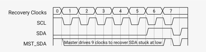
Figure 89 is a timing diagram illustrating the recovery of the SDA line when it is stuck at LOW. The diagram shows four signals over 8 clock cycles (0 to 7). The SCL signal is a periodic square wave. The SDA signal is initially low and then transitions high at clock 6. The MST_SDA signal is low until clock 6, then transitions high. A label indicates 'Master drives 9 clocks to recover SDA stuck at low'.
12.2.13.2. SCL line is stuck at LOW
In the unlikely event (due to an electric failure of a circuit) where the clock (SCL) is stuck to LOW, there is no effective method to overcome this problem. Instead, reset the bus using the hardware reset signal.
12.2.14. IC_CLK frequency configuration
When the DW_apb_i2c is configured as a Standard (SS), Fast (FS), or Fast-Mode Plus (FM+), the *CNT registers must be set before any I2C bus transaction can take place in order to ensure proper I/O timing. The *CNT registers are:
- • IC_SS_SCL_HCNT
- • IC_SS_SCL_LCNT
- • IC_FS_SCL_HCNT
- • IC_FS_SCL_LCNT
NOTE
The tBUF timing and setup/hold time of START, STOP and RESTART registers uses *HCNT/*LCNT register settings for the corresponding speed mode.
NOTEIt is not necessary to program any of the *CNT registers if the
DW_apb_i2c
is enabled to operate only as an I2C slave, since these registers are used only to determine the
SCL
timing requirements for operation as an I2C master.
Table 1052 lists the derivation of I2C timing parameters from the *CNT programming registers.
Table 1052. Derivation of I2C Timing Parameters from *CNT Registers
| Timing Parameter | Symbol | Standard Speed | Fast Speed / Fast Speed Plus |
|---|---|---|---|
LOW period of the
SCL
clock | tLOW | IC_SS_SCL_LCNT | IC_FS_SCL_LCNT |
HIGH period of the
SCL
clock | tHIGH | IC_SS_SCL_HCNT | IC_FS_SCL_HCNT |
| Setup time for a repeated START condition | tSU;STA | IC_SS_SCL_LCNT | IC_FS_SCL_HCNT |
| Hold time (repeated) START condition | tHD;STA | IC_SS_SCL_HCNT | IC_FS_SCL_HCNT |
| Setup time for STOP condition | tSU;STO | IC_SS_SCL_HCNT | IC_FS_SCL_HCNT |
| Bus free time between a STOP and a START condition | tBUF | IC_SS_SCL_LCNT | IC_FS_SCL_LCNT |
| Spike length | tSP | IC_FS_SPKLEN | IC_FS_SPKLEN |
| Data hold time | tHD;DAT | IC_SDA_HOLD | IC_SDA_HOLD |
| Data setup time | tSU;DAT | IC_SDA_SETUP | IC_SDA_SETUP |
12.2.14.1. Minimum high and low counts in SS, FS, and FM+ modes.
When the
DW_apb_i2c
operates as an I2C master, in both transmit and receive transfers:
- •
IC_SS_SCL_LCNTandIC_FS_SCL_LCNTregister values must be larger thanIC_FS_SPKLEN+ 7. - •
IC_SS_SCL_HCNTandIC_FS_SCL_HCNTregister values must be larger thanIC_FS_SPKLEN+ 5.
Details regarding the
DW_apb_i2c
high and low counts are as follows:
- • The minimum value of
IC_*_SPKLEN+ 7 for the *_LCNT registers is due to the time required for theDW_apb_i2cto driveSDAafter a negative edge ofSCL. - • The minimum value of
IC_*_SPKLEN+ 5 for the *_HCNT registers is due to the time required for theDW_apb_i2cto sampleSDAduring the high period ofSCL. - • The
DW_apb_i2cadds one cycle to the programmed *_LCNT value in order to generate the low period of theSCLclock; this is due to the counting logic forSCLlow counting to (*_LCNT + 1). - • The
DW_apb_i2caddsIC_*_SPKLEN+ 7 cycles to the programmed *_HCNT value in order to generate the high period of theSCLclock, due to the following factors:- ◦ The counting logic for
SCLhigh counts to (*_HCNT + 1). - ◦ The digital filtering applied to the
SCLline incurs a delay ofSPKLEN+ 2ic_clkcycles, whereSPKLENisIC_FS_SPKLENif the component is operating in SS or FS. - ◦ Whenever
SCLis driven one to zero by theDW_apb_i2c(completing theSCLhigh time) an internal logic latency of threeic_clkcycles is incurred. Consequently, the minimumSCLlow time of which theDW_apb_i2cis capable is nineic_clkperiods (7 + 1 + 1), while the minimumSCLhigh time is thirteenic_clkperiods (6 + 1 + 3 + 3).
- ◦ The counting logic for
NOTE
The total high time and low time of SCL generated by the DW_apb_i2c master is also influenced by the rise time and fall time of the SCL line, as shown in the illustration and equations in Figure 90 . SCL rise and fall time parameters vary depending on external factors such as:
- • Characteristics of the IO driver
- • Pull-up resistor value
- • Total capacitance on SCL line
These characteristics are beyond the control of the DW_apb_i2c .
Figure 90. Impact of SCL Rise Time and Fall Time on Generated SCL
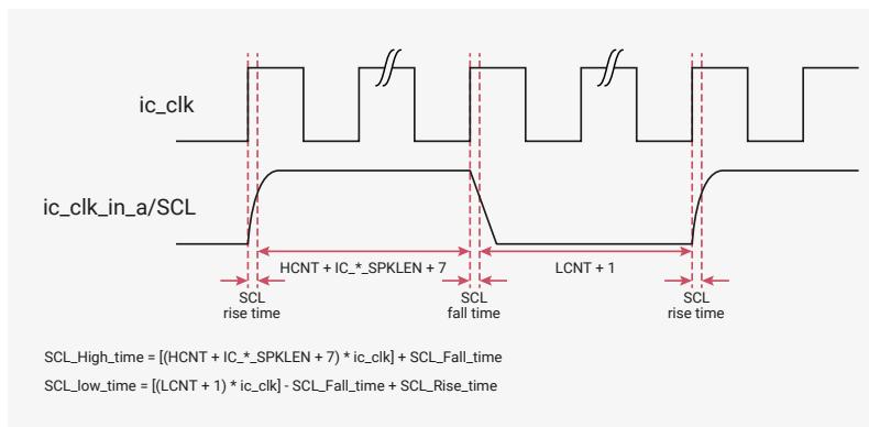
12.2.14.2. Minimum IC_CLK frequency
This section describes the minimum ic_clk frequencies that the DW_apb_i2c supports for each speed mode, and the associated high and low count values. In slave mode, IC_SDA_HOLD (Thd;dat) and IC_SDA_SETUP (Tsu;dat) need to be programmed to satisfy the I2C protocol timing requirements. The following examples are for the case where IC_FS_SPKLEN is programmed to two.
12.2.14.2.1. Standard Mode (SM), Fast Mode (FM), and Fast Mode Plus (FM+)
This section details how to derive a minimum ic_clk value for standard and fast modes of the DW_apb_i2c . Although the following method shows how to do fast mode calculations, you can also use the same method in order to do calculations for standard mode and fast mode plus.
NOTE
The following computations do not consider the SCL_Rise_time and SCL_Fall_time .
Given conditions and calculations for the minimum DW_apb_i2c ic_clk value in fast mode:
- • Fast mode has data rate of 400 kb/s; implies SCL period of 1/400 kHz = 2.5μs
- • Minimum hcnt value of 14 as a seed value; IC_HCNT_FS = 14
- • Protocol minimum
SCL
high and low times:
- ◦ MIN_SCL_LOWtime_FS = 1300 ns
- ◦ MIN_SCL_HIGHTime_FS = 600 ns
Derived equations:
Combined, the previous equations produce the following:
Solving for IC_LCNT_FS :
The previous equation gives:
These calculations produce IC_LCNT_FS = 16 and IC_HCNT_FS = 14 , giving an ic_clk value of:
Testing these results shows that protocol requirements are satisfied.
Table 1053 lists the minimum ic_clk values for all modes with high and low count values.
Table 1053. ic_clk in Relation to High and Low Counts
| Speed Mode | ic_clkfreq (MHz) | Minimum Value of IC_*_SPKLEN | SCL Low Time in 'ic_clk's | SCL Low Program Value | SCL Low Time | SCL High Time in 'ic_clk's | SCL High Program Value | SCL High Time |
|---|---|---|---|---|---|---|---|---|
| SS | 2.7 | 1 | 13 | 12 | 4.7μs | 14 | 6 | 5.2μs |
| FS | 12.0 | 1 | 16 | 15 | 1.33μs | 14 | 6 | 1.16μs |
| FM+ | 32 | 2 | 16 | 15 | 500 ns | 16 | 7 | 500 ns |
- The IC_*_SCL_LCNT and IC_*_SCL_HCNT registers are programmed using the SCL low and high program values in Table 1053 , which are calculated using SCL low count minus one, and SCL high counts minus eight, respectively. The values in Table 1053 are based on IC_SDA_RX_HOLD = 0. The maximum IC_SDA_RX_HOLD value depends on the IC_*CNT registers in Master mode.
- In order to compute the HCNT and LCNT considering RC timings, use the following equations:
- \( \text{IC\_HCNT\_}^* = [(\text{HCNT} + \text{IC\_}^*\text{SPKLEN} + 7) * \text{ic\_clk}] + \text{SCL\_Fall\_time} \)
- \( \text{IC\_LCNT\_}^* = [(\text{LCNT} + 1) * \text{ic\_clk}] - \text{SCL\_Fall\_time} + \text{SCL\_Rise\_time} \)
12.2.14.3. Calculating high and low counts
The calculations below show how to calculate SCL high and low counts for each speed mode in the DW_apb_i2c . For the calculations to work, the ic_clk frequencies used must not be less than the minimum ic_clk frequencies specified in Table 1053 .
The default ic_clk period value is set to 100 ns, so default SCL high and low count values are calculated for each speed
mode based on this clock. These values need updating according to the guidelines below.
The equation to calculate the proper number of
ic_clk
signals required for setting the proper
SCL
clocks high and low times is as follows:
IC_xCNT = (ROUNDUP(MIN_SCL_xxxtime*OSCFREQ,0))
MIN_SCL_HIGHtime = Minimum High Period
MIN_SCL_HIGHtime = 400ns for 100kb/s,
                  600ns for 400kb/s,
                  260ns for 1000kb/s,
MIN_SCL_LOWtime = Minimum Low Period
MIN_SCL_LOWtime = 470ns for 100kb/s,
                 1300ns for 400kb/s,
                 500ns for 1000kb/s,
OSCFREQ = ic_clk Clock Frequency (Hz).
For example:
OSCFREQ = 100MHz
I2Cmode = fast, 400kb/s
MIN_SCL_HIGHtime = 600ns.
MIN_SCL_LOWtime = 1300ns.
IC_xCNT = (ROUNDUP(MIN_SCL_HIGH_LOWtime*OSCFREQ,0))
IC_HCNT = (ROUNDUP(600ns * 100MHz,0))
IC_HCNTSCL PERIOD = 60
IC_LCNT = (ROUNDUP(1300ns * 100MHz,0))
IC_LCNTSCL PERIOD = 130
Actual MIN_SCL_HIGHtime = 60*(1/100MHz) = 600ns
Actual MIN_SCL_LOWtime = 130*(1/100MHz) = 1300ns
12.2.15. DMA controller interface
The
DW_apb_i2c
has built-in DMA capability; it has a handshaking interface to the DMA Controller to request and control transfers. The APB bus is used to perform data transfers to and from the DMA. DMA transfers use single accesses, since the data rate is relatively low.
12.2.15.1. Enabling the DMA controller interface
To enable the DMA Controller interface on the
DW_apb_i2c
, you must write the DMA Control Register (
IC_DMA_CR
). Writing a one into the
TDMAE
bit field of
IC_DMA_CR
register enables the
DW_apb_i2c
transmit handshaking interface. Writing a one into the
RDMAE
bit field of the
IC_DMA_CR
register enables the
DW_apb_i2c
receive handshaking interface.
12.2.15.2. Overview of operation
The DMA Controller is programmed with the number of data items (transfer count) that are to be transmitted or received by
DW_apb_i2c
.
The transfer is broken into single transfers on the bus, each initiated by a request from the
DW_apb_i2c
.
For example, where the transfer count programmed into the DMA Controller is four. The DMA transfer consists of a series of four single transactions. If the
DW_apb_i2c
makes a transmit request to this channel, a single data item is written to the
DW_apb_i2c
TX FIFO. Similarly, if the
DW_apb_i2c
makes a receive request to this channel, a single data item is read from the
DW_apb_i2c
RX FIFO. Four separate requests must be made to this DMA channel before all four data items are written or read.
12.2.15.3. Watermark levels
In
DW_apb_i2c
the registers for setting watermarks to allow DMA bursts do not need be set to anything other than their reset value. Specifically,
IC_DMA_TDLR
and
IC_DMA_RDLR
can be left at reset values of zero. This is because only single transfers are needed due to the low bandwidth of I2C relative to system bandwidth. Because the DMA controller normally has the highest priority on the system bus, transfers complete quickly.
12.2.16. Operation of interrupt registers
Table 1054 lists the operation of the
DW_apb_i2c
interrupt registers and how they are set and cleared. Some bits are set by hardware and cleared by software, whereas other bits are set and cleared by hardware.
Table 1054. Clearing and Setting of Interrupt Registers
| Interrupt Bit Fields | Set by Hardware/Cleared by Software | Set and Cleared by Hardware |
|---|---|---|
| RESTART_DET | Y | N |
| GEN_CALL | Y | N |
| START_DET | Y | N |
| STOP_DET | Y | N |
| ACTIVITY | Y | N |
| RX_DONE | Y | N |
| TX_ABRT | Y | N |
| RD_REQ | Y | N |
| TX_EMPTY | N | Y |
| TX_OVER | Y | N |
| RX_FULL | N | Y |
| RX_OVER | Y | N |
| RX_UNDER | Y | N |
12.2.17. List of registers
The I2C0 and I2C1 registers start at base addresses of
0x40090000
and
0x40098000
respectively (defined as
I2C0_BASE
and
I2C1_BASE
in SDK).
You may see references to configuration constants in the I2C register descriptions; these are fixed values, set at hardware design time. A full list of their values can be found in i2c.h in the pico-sdk GitHub repository .
Table 1055. List of I2C registers
| Offset | Name | Info |
|---|---|---|
| 0x00 | IC_CON | I2C Control Register |
| 0x04 | IC_TAR | I2C Target Address Register |
| 0x08 | IC_SAR | I2C Slave Address Register |
| 0x10 | IC_DATA_CMD | I2C Rx/Tx Data Buffer and Command Register |
| 0x14 | IC_SS_SCL_HCNT | Standard Speed I2C Clock SCL High Count Register |
| 0x18 | IC_SS_SCL_LCNT | Standard Speed I2C Clock SCL Low Count Register |
| 0x1c | IC_FS_SCL_HCNT | Fast Mode or Fast Mode Plus I2C Clock SCL High Count Register |
| 0x20 | IC_FS_SCL_LCNT | Fast Mode or Fast Mode Plus I2C Clock SCL Low Count Register |
| 0x2c | IC_INTR_STAT | I2C Interrupt Status Register |
| 0x30 | IC_INTR_MASK | I2C Interrupt Mask Register |
| 0x34 | IC_RAW_INTR_STAT | I2C Raw Interrupt Status Register |
| 0x38 | IC_RX_TL | I2C Receive FIFO Threshold Register |
| 0x3c | IC_TX_TL | I2C Transmit FIFO Threshold Register |
| 0x40 | IC_CLR_INTR | Clear Combined and Individual Interrupt Register |
| 0x44 | IC_CLR_RX_UNDER | Clear RX_UNDER Interrupt Register |
| 0x48 | IC_CLR_RX_OVER | Clear RX_OVER Interrupt Register |
| 0x4c | IC_CLR_TX_OVER | Clear TX_OVER Interrupt Register |
| 0x50 | IC_CLR_RD_REQ | Clear RD_REQ Interrupt Register |
| 0x54 | IC_CLR_TX_ABRT | Clear TX_ABRT Interrupt Register |
| 0x58 | IC_CLR_RX_DONE | Clear RX_DONE Interrupt Register |
| 0x5c | IC_CLR_ACTIVITY | Clear ACTIVITY Interrupt Register |
| 0x60 | IC_CLR_STOP_DET | Clear STOP_DET Interrupt Register |
| 0x64 | IC_CLR_START_DET | Clear START_DET Interrupt Register |
| 0x68 | IC_CLR_GEN_CALL | Clear GEN_CALL Interrupt Register |
| 0x6c | IC_ENABLE | I2C ENABLE Register |
| 0x70 | IC_STATUS | I2C STATUS Register |
| 0x74 | IC_TXFLR | I2C Transmit FIFO Level Register |
| 0x78 | IC_RXFLR | I2C Receive FIFO Level Register |
| 0x7c | IC_SDA_HOLD | I2C SDA Hold Time Length Register |
| 0x80 | IC_TX_ABRT_SOURCE | I2C Transmit Abort Source Register |
| 0x84 | IC_SLV_DATA_NACK_ONLY | Generate Slave Data NACK Register |
| 0x88 | IC_DMA_CR | DMA Control Register |
| Offset | Name | Info |
|---|---|---|
| 0x8c | IC_DMA_TDLR | DMA Transmit Data Level Register |
| 0x90 | IC_DMA_RDLR | DMA Transmit Data Level Register |
| 0x94 | IC_SDA_SETUP | I2C SDA Setup Register |
| 0x98 | IC_ACK_GENERAL_CALL | I2C ACK General Call Register |
| 0x9c | IC_ENABLE_STATUS | I2C Enable Status Register |
| 0xa0 | IC_FS_SPKLEN | I2C SS, FS or FM+ spike suppression limit |
| 0xa8 | IC_CLR_RESTART_DET | Clear RESTART_DET Interrupt Register |
| 0xf4 | IC_COMP_PARAM_1 | Component Parameter Register 1 |
| 0xf8 | IC_COMP_VERSION | I2C Component Version Register |
| 0xfc | IC_COMP_TYPE | I2C Component Type Register |
I2C: IC_CON Register
Offset: 0x00
Description
I2C Control Register. This register can be written only when the DW_apb_i2c is disabled, which corresponds to the IC_ENABLE[0] register being set to 0. Writes at other times have no effect.
Read/Write Access: - bit 10 is read only - bit 11 is read only - bit 16 is read only - bit 17 is read only - bits 18 and 19 are read only.
Table 1056. IC_CON Register
| Bits | Description | Type | Reset |
|---|---|---|---|
| 31:11 | Reserved. | - | - |
| 10 | STOP_DET_IF_MASTER_ACTIVE: Master issues the STOP_DET interrupt irrespective of whether master is active or not | RO | 0x0 |
| 9 | RX_FIFO_FULL_HLD_CTRL:
This bit controls whether DW_apb_i2c should hold the bus when the Rx FIFO is physically full to its RX_BUFFER_DEPTH, as described in the IC_RX_FULL_HLD_BUS_EN parameter. Reset value: 0x0. | RW | 0x0 |
| Enumerated values: | |||
| 0x0 → DISABLED: Overflow when RX_FIFO is full | |||
| 0x1 → ENABLED: Hold bus when RX_FIFO is full | |||
| 8 | TX_EMPTY_CTRL:
This bit controls the generation of the TX_EMPTY interrupt, as described in the IC_RAW_INTR_STAT register. Reset value: 0x0. | RW | 0x0 |
| Enumerated values: | |||
| 0x0 → DISABLED: Default behaviour of TX_EMPTY interrupt | |||
| 0x1 → ENABLED: Controlled generation of TX_EMPTY interrupt |
| Bits | Description | Type | Reset |
|---|---|---|---|
| 7 | STOP_DET_IFADDRESSED: In slave mode: - 1'b1: issues the STOP_DET interrupt only when it is addressed. - 1'b0: issues the STOP_DET irrespective of whether it's addressed or not. Reset value: 0x0 NOTE: During a general call address, this slave does not issue the STOP_DET interrupt if STOP_DET_IF_ADDRESSED = 1'b1, even if the slave responds to the general call address by generating ACK. The STOP_DET interrupt is generated only when the transmitted address matches the slave address (SAR). | RW | 0x0 |
| Enumerated values: | |||
| 0x0 → DISABLED: slave issues STOP_DET intr always | |||
| 0x1 → ENABLED: slave issues STOP_DET intr only if addressed | |||
| 6 | IC_SLAVE_DISABLE: This bit controls whether I2C has its slave disabled, which means once the preseln signal is applied, then this bit is set and the slave is disabled. If this bit is set (slave is disabled), DW_apb_i2c functions only as a master and does not perform any action that requires a slave. NOTE: Software should ensure that if this bit is written with 0, then bit 0 should also be written with a 0. | RW | 0x1 |
| Enumerated values: | |||
| 0x0 → SLAVE_ENABLED: Slave mode is enabled | |||
| 0x1 → SLAVE_DISABLED: Slave mode is disabled | |||
| 5 | IC_RESTART_EN: Determines whether RESTART conditions may be sent when acting as a master. Some older slaves do not support handling RESTART conditions; however, RESTART conditions are used in several DW_apb_i2c operations. When RESTART is disabled, the master is prohibited from performing the following functions: - Sending a START BYTE - Performing any high-speed mode operation - High-speed mode operation - Performing direction changes in combined format mode - Performing a read operation with a 10-bit address By replacing RESTART condition followed by a STOP and a subsequent START condition, split operations are broken down into multiple DW_apb_i2c transfers. If the above operations are performed, it will result in setting bit 6 (TX_ABRT) of the IC_RAW_INTR_STAT register. Reset value: ENABLED | RW | 0x1 |
| Enumerated values: | |||
| 0x0 → DISABLED: Master restart disabled | |||
| 0x1 → ENABLED: Master restart enabled | |||
| 4 | IC_10BITADDR_MASTER: Controls whether the DW_apb_i2c starts its transfers in 7- or 10-bit addressing mode when acting as a master. - 0: 7-bit addressing - 1: 10-bit addressing | RW | 0x0 |
| Enumerated values: | |||
| 0x0 → ADDR_7BITS: Master 7Bit addressing mode | |||
| 0x1 → ADDR_10BITS: Master 10Bit addressing mode |
| Bits | Description | Type | Reset |
|---|---|---|---|
| 3 | IC_10BITADDR_SLAVE: When acting as a slave, this bit controls whether the DW_apb_i2c responds to 7- or 10-bit addresses. - 0: 7-bit addressing. The DW_apb_i2c ignores transactions that involve 10-bit addressing; for 7-bit addressing, only the lower 7 bits of the IC_SAR register are compared. - 1: 10-bit addressing. The DW_apb_i2c responds to only 10-bit addressing transfers that match the full 10 bits of the IC_SAR register. | RW | 0x0 |
| Enumerated values: | |||
| 0x0 → ADDR_7BITS: Slave 7Bit addressing | |||
| 0x1 → ADDR_10BITS: Slave 10Bit addressing | |||
| 2:1 | SPEED:
These bits control at which speed the DW_apb_i2c operates; its setting is relevant only if one is operating the DW_apb_i2c in master mode. Hardware protects against illegal values being programmed by software. These bits must be programmed appropriately for slave mode also, as it is used to capture correct value of spike filter as per the speed mode. This register should be programmed only with a value in the range of 1 to IC_MAX_SPEED_MODE; otherwise, hardware updates this register with the value of IC_MAX_SPEED_MODE. 1: standard mode (100 kbit/s) 2: fast mode (<=400 kbit/s) or fast mode plus (<=1000Kbit/s) 3: high speed mode (3.4 Mbit/s) Note: This field is not applicable when IC_ULTRA_FAST_MODE=1 | RW | 0x2 |
| Enumerated values: | |||
| 0x1 → STANDARD: Standard Speed mode of operation | |||
| 0x2 → FAST: Fast or Fast Plus mode of operation | |||
| 0x3 → HIGH: High Speed mode of operation | |||
| 0 | MASTER_MODE:
This bit controls whether the DW_apb_i2c master is enabled. NOTE: Software should ensure that if this bit is written with '1' then bit 6 should also be written with a '1'. | RW | 0x1 |
| Enumerated values: | |||
| 0x0 → DISABLED: Master mode is disabled | |||
| 0x1 → ENABLED: Master mode is enabled |
I2C: IC_TAR Register
Offset: 0x04
Description
I2C Target Address Register
This register is 12 bits wide, and bits 31:12 are reserved. This register can be written to only when IC_ENABLE[0] is set to 0.
Note: If the software or application is aware that the DW_apb_i2c is not using the TAR address for the pending
commands in the Tx FIFO, then it is possible to update the TAR address even while the Tx FIFO has entries (IC_STATUS[2]= 0). - It is not necessary to perform any write to this register if DW_apb_i2c is enabled as an I2C slave only.
Table 1057. IC_TAR Register
| Bits | Description | Type | Reset |
|---|---|---|---|
| 31:12 | Reserved. | - | - |
| 11 | SPECIAL: This bit indicates whether software performs a Device-ID or General Call or START BYTE command. - 0: ignore bit 10 GC_OR_START and use IC_TAR normally - 1: perform special I2C command as specified in Device_ID or GC_OR_START bit Reset value: 0x0 | RW | 0x0 |
| Enumerated values: | |||
| 0x0 → DISABLED: Disables programming of GENERAL_CALL or START_BYTE transmission | |||
| 0x1 → ENABLED: Enables programming of GENERAL_CALL or START_BYTE transmission | |||
| 10 | GC_OR_START: If bit 11 (SPECIAL) is set to 1 and bit 13(Device-ID) is set to 0, then this bit indicates whether a General Call or START byte command is to be performed by the DW_apb_i2c. - 0: General Call Address - after issuing a General Call, only writes may be performed. Attempting to issue a read command results in setting bit 6 (TX_ABRT) of the IC_RAW_INTR_STAT register. The DW_apb_i2c remains in General Call mode until the SPECIAL bit value (bit 11) is cleared. - 1: START BYTE Reset value: 0x0 | RW | 0x0 |
| Enumerated values: | |||
| 0x0 → GENERAL_CALL: GENERAL_CALL byte transmission | |||
| 0x1 → START_BYTE: START byte transmission | |||
| 9:0 | IC_TAR:
This is the target address for any master transaction. When transmitting a General Call, these bits are ignored. To generate a START BYTE, the CPU needs to write only once into these bits. If the IC_TAR and IC_SAR are the same, loopback exists but the FIFOs are shared between master and slave, so full loopback is not feasible. Only one direction loopback mode is supported (simplex), not duplex. A master cannot transmit to itself; it can transmit to only a slave. | RW | 0x055 |
I2C: IC_SAR Register
Offset: 0x08
Description
I2C Slave Address Register
Table 1058. IC_SAR Register
| Bits | Description | Type | Reset |
|---|---|---|---|
| 31:10 | Reserved. | - | - |
| Bits | Description | Type | Reset |
|---|---|---|---|
| 9:0 | IC_SAR: The IC_SAR holds the slave address when the I2C is operating as a slave. For 7-bit addressing, only IC_SAR[6:0] is used. This register can be written only when the I2C interface is disabled, which corresponds to the IC_ENABLE[0] register being set to 0. Writes at other times have no effect. Note: The default values cannot be any of the reserved address locations: that is, 0x00 to 0x07, or 0x78 to 0x7f. The correct operation of the device is not guaranteed if you program the IC_SAR or IC_TAR to a reserved value. Refer to Table 1051 for a complete list of these reserved values. | RW | 0x055 |
I2C: IC_DATA_CMD Register
Offset: 0x10
Description
I2C Rx/Tx Data Buffer and Command Register; this is the register the CPU writes to when filling the TX FIFO and the CPU reads from when retrieving bytes from RX FIFO.
The size of the register changes as follows:
Write: - 11 bits when IC_EMPTYFIFO_HOLD_MASTER_EN=1 - 9 bits when IC_EMPTYFIFO_HOLD_MASTER_EN=0 Read: - 12 bits when IC_FIRST_DATA_BYTE_STATUS = 1 - 8 bits when IC_FIRST_DATA_BYTE_STATUS = 0 Note: In order for the DW_apb_i2c to continue acknowledging reads, a read command should be written for every byte that is to be received; otherwise the DW_apb_i2c will stop acknowledging.
Table 1059.
IC_DATA_CMD
Register
| Bits | Description | Type | Reset |
|---|---|---|---|
| 31:12 | Reserved. | - | - |
| 11 | FIRST_DATA_BYTE: Indicates the first data byte received after the address phase for receive transfer in Master receiver or Slave receiver mode. Reset value : 0x0 NOTE: In case of APB_DATA_WIDTH=8,
| RO | 0x0 |
| Enumerated values: | |||
| 0x0 → INACTIVE: Sequential data byte received | |||
| 0x1 → ACTIVE: Non sequential data byte received |
| Bits | Description | Type | Reset |
|---|---|---|---|
| 10 | RESTART: This bit controls whether a RESTART is issued before the byte is sent or received. 1 - If IC_RESTART_EN is 1, a RESTART is issued before the data is sent/received (according to the value of CMD), regardless of whether or not the transfer direction is changing from the previous command; if IC_RESTART_EN is 0, a STOP followed by a START is issued instead. 0 - If IC_RESTART_EN is 1, a RESTART is issued only if the transfer direction is changing from the previous command; if IC_RESTART_EN is 0, a STOP followed by a START is issued instead. Reset value: 0x0 | SC | 0x0 |
| Enumerated values: | |||
| 0x0 → DISABLE: Don't Issue RESTART before this command | |||
| 0x1 → ENABLE: Issue RESTART before this command | |||
| 9 | STOP: This bit controls whether a STOP is issued after the byte is sent or received. - 1 - STOP is issued after this byte, regardless of whether or not the Tx FIFO is empty. If the Tx FIFO is not empty, the master immediately tries to start a new transfer by issuing a START and arbitrating for the bus. - 0 - STOP is not issued after this byte, regardless of whether or not the Tx FIFO is empty. If the Tx FIFO is not empty, the master continues the current transfer by sending/receiving data bytes according to the value of the CMD bit. If the Tx FIFO is empty, the master holds the SCL line low and stalls the bus until a new command is available in the Tx FIFO. Reset value: 0x0 | SC | 0x0 |
| Enumerated values: | |||
| 0x0 → DISABLE: Don't Issue STOP after this command | |||
| 0x1 → ENABLE: Issue STOP after this command | |||
| 8 | CMD: This bit controls whether a read or a write is performed. This bit does not control the direction when the DW_apb_i2con acts as a slave. It controls only the direction when it acts as a master. When a command is entered in the TX FIFO, this bit distinguishes the write and read commands. In slave-receiver mode, this bit is a 'don't care' because writes to this register are not required. In slave-transmitter mode, a '0' indicates that the data in IC_DATA_CMD is to be transmitted. When programming this bit, you should remember the following: attempting to perform a read operation after a General Call command has been sent results in a TX_ABRT interrupt (bit 6 of the IC_RAW_INTR_STAT register), unless bit 11 (SPECIAL) in the IC_TAR register has been cleared. If a '1' is written to this bit after receiving a RD_REQ interrupt, then a TX_ABRT interrupt occurs. Reset value: 0x0 | SC | 0x0 |
| Enumerated values: | |||
| 0x0 → WRITE: Master Write Command |
| Bits | Description | Type | Reset |
|---|---|---|---|
| 0x1 → READ: Master Read Command | |||
| 7:0 | DAT
: This register contains the data to be transmitted or received on the I2C bus. If you are writing to this register and want to perform a read, bits 7:0 (DAT) are ignored by the DW_apb_i2c. However, when you read this register, these bits return the value of data received on the DW_apb_i2c interface. Reset value: 0x0 | RW | 0x00 |
I2C: IC_SS_SCL_HCNT Register
Offset: 0x14
Description
Standard Speed I2C Clock SCL High Count Register
Table 1060.
IC_SS_SCL_HCNT
Register
| Bits | Description | Type | Reset |
|---|---|---|---|
| 31:16 | Reserved. | - | - |
| 15:0 | IC_SS_SCL_HCNT
: This register must be set before any I2C bus transaction can take place to ensure proper I/O timing. This register sets the SCL clock high-period count for standard speed. For more information, refer to 'IC_CLK Frequency Configuration'. This register can be written only when the I2C interface is disabled which corresponds to the IC_ENABLE[0] register being set to 0. Writes at other times have no effect. The minimum valid value is 6; hardware prevents values less than this being written, and if attempted results in 6 being set. For designs with APB_DATA_WIDTH = 8, the order of programming is important to ensure the correct operation of the DW_apb_i2c. The lower byte must be programmed first. Then the upper byte is programmed. NOTE: This register must not be programmed to a value higher than 65525, because DW_apb_i2c uses a 16-bit counter to flag an I2C bus idle condition when this counter reaches a value of IC_SS_SCL_HCNT + 10. | RW | 0x0028 |
I2C: IC_SS_SCL_LCNT Register
Offset: 0x18
Description
Standard Speed I2C Clock SCL Low Count Register
Table 1061.
IC_SS_SCL_LCNT
Register
| Bits | Description | Type | Reset |
|---|---|---|---|
| 31:16 | Reserved. | - | - |
| Bits | Description | Type | Reset |
|---|---|---|---|
| 15:0 | IC_FS_SCL_LCNT: This register must be set before any I2C bus transaction can take place to ensure proper I/O timing. This register sets the SCL clock low period count for fast speed. It is used in high-speed mode to send the Master Code and START BYTE or General CALL. For more information, refer to 'IC_CLK Frequency Configuration'. This register goes away and becomes read-only returning 0s if IC_MAX_SPEED_MODE = standard. This register can be written only when the I2C interface is disabled, which corresponds to the IC_ENABLE[0] register being set to 0. Writes at other times have no effect. The minimum valid value is 8; hardware prevents values less than this being written, and if attempted results in 8 being set. For designs with APB_DATA_WIDTH = 8 the order of programming is important to ensure the correct operation of the DW_apb_i2c. The lower byte must be programmed first. Then the upper byte is programmed. If the value is less than 8 then the count value gets changed to 8. | RW | 0x000d |
I2C: IC_INTR_STAT Register
Offset: 0x2c
Description
I2C Interrupt Status Register
Each bit in this register has a corresponding mask bit in the IC_INTR_MASK register. These bits are cleared by reading the matching interrupt clear register. The unmasked raw versions of these bits are available in the IC_RAW_INTR_STAT register.
Table 1064.
IC_INTR_STAT
Register
| Bits | Description | Type | Reset |
|---|---|---|---|
| 31:13 | Reserved. | - | - |
| 12 | R_RESTART_DET: See IC_RAW_INTR_STAT for a detailed description of R_RESTART_DET bit. Reset value: 0x0 Enumerated values: 0x0 → INACTIVE: R_RESTART_DET interrupt is inactive 0x1 → ACTIVE: R_RESTART_DET interrupt is active | RO | 0x0 |
| 11 | R_GEN_CALL: See IC_RAW_INTR_STAT for a detailed description of R_GEN_CALL bit. Reset value: 0x0 Enumerated values: 0x0 → INACTIVE: R_GEN_CALL interrupt is inactive 0x1 → ACTIVE: R_GEN_CALL interrupt is active | RO | 0x0 |
| Bits | Description | Type | Reset |
|---|---|---|---|
| 10 | R_START_DET:
See IC_RAW_INTR_STAT for a detailed description of R_START_DET bit. Reset value: 0x0 | RO | 0x0 |
| Enumerated values: | |||
| 0x0 → INACTIVE: R_START_DET interrupt is inactive | |||
| 0x1 → ACTIVE: R_START_DET interrupt is active | |||
| 9 | R_STOP_DET:
See IC_RAW_INTR_STAT for a detailed description of R_STOP_DET bit. Reset value: 0x0 | RO | 0x0 |
| Enumerated values: | |||
| 0x0 → INACTIVE: R_STOP_DET interrupt is inactive | |||
| 0x1 → ACTIVE: R_STOP_DET interrupt is active | |||
| 8 | R_ACTIVITY:
See IC_RAW_INTR_STAT for a detailed description of R_ACTIVITY bit. Reset value: 0x0 | RO | 0x0 |
| Enumerated values: | |||
| 0x0 → INACTIVE: R_ACTIVITY interrupt is inactive | |||
| 0x1 → ACTIVE: R_ACTIVITY interrupt is active | |||
| 7 | R_RX_DONE:
See IC_RAW_INTR_STAT for a detailed description of R_RX_DONE bit. Reset value: 0x0 | RO | 0x0 |
| Enumerated values: | |||
| 0x0 → INACTIVE: R_RX_DONE interrupt is inactive | |||
| 0x1 → ACTIVE: R_RX_DONE interrupt is active | |||
| 6 | R_TX_ABRT:
See IC_RAW_INTR_STAT for a detailed description of R_TX_ABRT bit. Reset value: 0x0 | RO | 0x0 |
| Enumerated values: | |||
| 0x0 → INACTIVE: R_TX_ABRT interrupt is inactive | |||
| 0x1 → ACTIVE: R_TX_ABRT interrupt is active | |||
| 5 | R_RD_REQ:
See IC_RAW_INTR_STAT for a detailed description of R_RD_REQ bit. Reset value: 0x0 | RO | 0x0 |
| Enumerated values: | |||
| 0x0 → INACTIVE: R_RD_REQ interrupt is inactive | |||
| 0x1 → ACTIVE: R_RD_REQ interrupt is active |
| Bits | Description | Type | Reset |
|---|---|---|---|
| 4 | R_TX_EMPTY:
See IC_RAW_INTR_STAT for a detailed description of R_TX_EMPTY bit. Reset value: 0x0 | RO | 0x0 |
| Enumerated values: | |||
| 0x0 → INACTIVE: R_TX_EMPTY interrupt is inactive | |||
| 0x1 → ACTIVE: R_TX_EMPTY interrupt is active | |||
| 3 | R_TX_OVER:
See IC_RAW_INTR_STAT for a detailed description of R_TX_OVER bit. Reset value: 0x0 | RO | 0x0 |
| Enumerated values: | |||
| 0x0 → INACTIVE: R_TX_OVER interrupt is inactive | |||
| 0x1 → ACTIVE: R_TX_OVER interrupt is active | |||
| 2 | R_RX_FULL:
See IC_RAW_INTR_STAT for a detailed description of R_RX_FULL bit. Reset value: 0x0 | RO | 0x0 |
| Enumerated values: | |||
| 0x0 → INACTIVE: R_RX_FULL interrupt is inactive | |||
| 0x1 → ACTIVE: R_RX_FULL interrupt is active | |||
| 1 | R_RX_OVER:
See IC_RAW_INTR_STAT for a detailed description of R_RX_OVER bit. Reset value: 0x0 | RO | 0x0 |
| Enumerated values: | |||
| 0x0 → INACTIVE: R_RX_OVER interrupt is inactive | |||
| 0x1 → ACTIVE: R_RX_OVER interrupt is active | |||
| 0 | R_RX_UNDER:
See IC_RAW_INTR_STAT for a detailed description of R_RX_UNDER bit. Reset value: 0x0 | RO | 0x0 |
| Enumerated values: | |||
| 0x0 → INACTIVE: RX_UNDER interrupt is inactive | |||
| 0x1 → ACTIVE: RX_UNDER interrupt is active |
I2C: IC_INTR_MASK Register
Offset: 0x30
Description
I2C Interrupt Mask Register.
These bits mask their corresponding interrupt status bits. This register is active low; a value of 0 masks the interrupt, whereas a value of 1 unmasks the interrupt.
Table 1065.
IC_INTR_MASK
Register
| Bits | Description | Type | Reset |
|---|---|---|---|
| 31:13 | Reserved. | - | - |
| 12 | M_RESTART_DET
: This bit masks the R_RESTART_DET interrupt in IC_INTR_STAT register. Reset value: 0x0 | RW | 0x0 |
| Enumerated values: | |||
| 0x0 → ENABLED: RESTART_DET interrupt is masked | |||
| 0x1 → DISABLED: RESTART_DET interrupt is unmasked | |||
| 11 | M_GEN_CALL
: This bit masks the R_GEN_CALL interrupt in IC_INTR_STAT register. Reset value: 0x1 | RW | 0x1 |
| Enumerated values: | |||
| 0x0 → ENABLED: GEN_CALL interrupt is masked | |||
| 0x1 → DISABLED: GEN_CALL interrupt is unmasked | |||
| 10 | M_START_DET
: This bit masks the R_START_DET interrupt in IC_INTR_STAT register. Reset value: 0x0 | RW | 0x0 |
| Enumerated values: | |||
| 0x0 → ENABLED: START_DET interrupt is masked | |||
| 0x1 → DISABLED: START_DET interrupt is unmasked | |||
| 9 | M_STOP_DET
: This bit masks the R_STOP_DET interrupt in IC_INTR_STAT register. Reset value: 0x0 | RW | 0x0 |
| Enumerated values: | |||
| 0x0 → ENABLED: STOP_DET interrupt is masked | |||
| 0x1 → DISABLED: STOP_DET interrupt is unmasked | |||
| 8 | M_ACTIVITY
: This bit masks the R_ACTIVITY interrupt in IC_INTR_STAT register. Reset value: 0x0 | RW | 0x0 |
| Enumerated values: | |||
| 0x0 → ENABLED: ACTIVITY interrupt is masked | |||
| 0x1 → DISABLED: ACTIVITY interrupt is unmasked | |||
| 7 | M_RX_DONE
: This bit masks the R_RX_DONE interrupt in IC_INTR_STAT register. Reset value: 0x1 | RW | 0x1 |
| Enumerated values: | |||
| 0x0 → ENABLED: RX_DONE interrupt is masked |
| Bits | Description | Type | Reset |
|---|---|---|---|
| 0x1 → DISABLED: RX_DONE interrupt is unmasked | |||
| 6 | M_TX_ABORT
: This bit masks the R_TX_ABORT interrupt in IC_INTR_STAT register. Reset value: 0x1 | RW | 0x1 |
| Enumerated values: | |||
| 0x0 → ENABLED: TX_ABORT interrupt is masked | |||
| 0x1 → DISABLED: TX_ABORT interrupt is unmasked | |||
| 5 | M_RD_REQ
: This bit masks the R_RD_REQ interrupt in IC_INTR_STAT register. Reset value: 0x1 | RW | 0x1 |
| Enumerated values: | |||
| 0x0 → ENABLED: RD_REQ interrupt is masked | |||
| 0x1 → DISABLED: RD_REQ interrupt is unmasked | |||
| 4 | M_TX_EMPTY
: This bit masks the R_TX_EMPTY interrupt in IC_INTR_STAT register. Reset value: 0x1 | RW | 0x1 |
| Enumerated values: | |||
| 0x0 → ENABLED: TX_EMPTY interrupt is masked | |||
| 0x1 → DISABLED: TX_EMPTY interrupt is unmasked | |||
| 3 | M_TX_OVER
: This bit masks the R_TX_OVER interrupt in IC_INTR_STAT register. Reset value: 0x1 | RW | 0x1 |
| Enumerated values: | |||
| 0x0 → ENABLED: TX_OVER interrupt is masked | |||
| 0x1 → DISABLED: TX_OVER interrupt is unmasked | |||
| 2 | M_RX_FULL
: This bit masks the R_RX_FULL interrupt in IC_INTR_STAT register. Reset value: 0x1 | RW | 0x1 |
| Enumerated values: | |||
| 0x0 → ENABLED: RX_FULL interrupt is masked | |||
| 0x1 → DISABLED: RX_FULL interrupt is unmasked | |||
| 1 | M_RX_OVER
: This bit masks the R_RX_OVER interrupt in IC_INTR_STAT register. Reset value: 0x1 | RW | 0x1 |
| Enumerated values: | |||
| 0x0 → ENABLED: RX_OVER interrupt is masked | |||
| 0x1 → DISABLED: RX_OVER interrupt is unmasked |
| Bits | Description | Type | Reset |
|---|---|---|---|
| 0 | M_RX_UNDER
: This bit masks the R_RX_UNDER interrupt in IC_INTR_STAT register. Reset value: 0x1 | RW | 0x1 |
| Enumerated values: | |||
| 0x0 → ENABLED: RX_UNDER interrupt is masked | |||
| 0x1 → DISABLED: RX_UNDER interrupt is unmasked |
I2C: IC_RAW_INTR_STAT Register
Offset: 0x34
Description
I2C Raw Interrupt Status Register
Unlike the IC_INTR_STAT register, these bits are not masked so they always show the true status of the DW_apb_i2c.
Table 1066.
IC_RAW_INTR_STAT
Register
| Bits | Description | Type | Reset |
|---|---|---|---|
| 31:13 | Reserved. | - | - |
| 12 | RESTART_DET
: Indicates whether a RESTART condition has occurred on the I2C interface when DW_apb_i2c is operating in Slave mode and the slave is being addressed. Enabled only when IC_SLV_RESTART_DET_EN=1. Note: However, in high-speed mode or during a START BYTE transfer, the RESTART comes before the address field as per the I2C protocol. In this case, the slave is not the addressed slave when the RESTART is issued, therefore DW_apb_i2c does not generate the RESTART_DET interrupt. Reset value: 0x0 | RO | 0x0 |
| Enumerated values: | |||
| 0x0 → INACTIVE: RESTART_DET interrupt is inactive | |||
| 0x1 → ACTIVE: RESTART_DET interrupt is active | |||
| 11 | GEN_CALL
: Set only when a General Call address is received and it is acknowledged. It stays set until it is cleared either by disabling DW_apb_i2c or when the CPU reads bit 0 of the IC_CLR_GEN_CALL register. DW_apb_i2c stores the received data in the Rx buffer. Reset value: 0x0 | RO | 0x0 |
| Enumerated values: | |||
| 0x0 → INACTIVE: GEN_CALL interrupt is inactive | |||
| 0x1 → ACTIVE: GEN_CALL interrupt is active | |||
| 10 | START_DET
: Indicates whether a START or RESTART condition has occurred on the I2C interface regardless of whether DW_apb_i2c is operating in slave or master mode. Reset value: 0x0 | RO | 0x0 |
| Enumerated values: |
| Bits | Description | Type | Reset |
|---|---|---|---|
| 0x0 → INACTIVE: START_DET interrupt is inactive | |||
| 0x1 → ACTIVE: START_DET interrupt is active | |||
| 9 | STOP_DET: Indicates whether a STOP condition has occurred on the I2C interface regardless of whether DW_apb_i2c is operating in slave or master mode. In Slave Mode: - If IC_CON[7]=1'b1 (STOP_DET_IFADDRESSED), the STOP_DET interrupt will be issued only if slave is addressed. Note: During a general call address, this slave does not issue a STOP_DET interrupt if STOP_DET_IF_ADDRESSED=1'b1, even if the slave responds to the general call address by generating ACK. The STOP_DET interrupt is generated only when the transmitted address matches the slave address (SAR). - If IC_CON[7]=1'b0 (STOP_DET_IFADDRESSED), the STOP_DET interrupt is issued irrespective of whether it is being addressed. In Master Mode: - If IC_CON[10]=1'b1 (STOP_DET_IF_MASTER_ACTIVE), the STOP_DET interrupt will be issued only if Master is active. - If IC_CON[10]=1'b0 (STOP_DET_IFADDRESSED), the STOP_DET interrupt will be issued irrespective of whether master is active or not. Reset value: 0x0 | RO | 0x0 |
| Enumerated values: | |||
| 0x0 → INACTIVE: STOP_DET interrupt is inactive | |||
| 0x1 → ACTIVE: STOP_DET interrupt is active | |||
| 8 | ACTIVITY: This bit captures DW_apb_i2c activity and stays set until it is cleared. There are four ways to clear it: - Disabling the DW_apb_i2c - Reading the IC_CLR_ACTIVITY register - Reading the IC_CLR_INTR register - System reset Once this bit is set, it stays set unless one of the four methods is used to clear it. Even if the DW_apb_i2c module is idle, this bit remains set until cleared, indicating that there was activity on the bus. Reset value: 0x0 | RO | 0x0 |
| Enumerated values: | |||
| 0x0 → INACTIVE: RAW_INTR_ACTIVITY interrupt is inactive | |||
| 0x1 → ACTIVE: RAW_INTR_ACTIVITY interrupt is active | |||
| 7 | RX_DONE: When the DW_apb_i2c is acting as a slave-transmitter, this bit is set to 1 if the master does not acknowledge a transmitted byte. This occurs on the last byte of the transmission, indicating that the transmission is done. Reset value: 0x0 | RO | 0x0 |
| Enumerated values: | |||
| 0x0 → INACTIVE: RX_DONE interrupt is inactive | |||
| 0x1 → ACTIVE: RX_DONE interrupt is active |
| Bits | Description | Type | Reset |
|---|---|---|---|
| 6 | TX_ABRT: This bit indicates if DW_apb_i2c, as an I2C transmitter, is unable to complete the intended actions on the contents of the transmit FIFO. This situation can occur both as an I2C master or an I2C slave, and is referred to as a 'transmit abort'. When this bit is set to 1, the IC_TX_ABRT_SOURCE register indicates the reason why the transmit abort takes places. Note: The DW_apb_i2c flushes/resets/empties the TX_FIFO and RX_FIFO whenever there is a transmit abort caused by any of the events tracked by the IC_TX_ABRT_SOURCE register. The FIFOs remains in this flushed state until the register IC_CLR_TX_ABRT is read. Once this read is performed, the Tx FIFO is then ready to accept more data bytes from the APB interface. Reset value: 0x0 | RO | 0x0 |
| Enumerated values: | |||
| 0x0 → INACTIVE: TX_ABRT interrupt is inactive | |||
| 0x1 → ACTIVE: TX_ABRT interrupt is active | |||
| 5 | RD_REQ: This bit is set to 1 when DW_apb_i2c is acting as a slave and another I2C master is attempting to read data from DW_apb_i2c. The DW_apb_i2c holds the I2C bus in a wait state (SCL=0) until this interrupt is serviced, which means that the slave has been addressed by a remote master that is asking for data to be transferred. The processor must respond to this interrupt and then write the requested data to the IC_DATA_CMD register. This bit is set to 0 just after the processor reads the IC_CLR_RD_REQ register. Reset value: 0x0 | RO | 0x0 |
| Enumerated values: | |||
| 0x0 → INACTIVE: RD_REQ interrupt is inactive | |||
| 0x1 → ACTIVE: RD_REQ interrupt is active | |||
| 4 | TX_EMPTY: The behavior of the TX_EMPTY interrupt status differs based on the TX_EMPTY_CTRL selection in the IC_CON register. - When TX_EMPTY_CTRL = 0: This bit is set to 1 when the transmit buffer is at or below the threshold value set in the IC_TX_TL register. - When TX_EMPTY_CTRL = 1: This bit is set to 1 when the transmit buffer is at or below the threshold value set in the IC_TX_TL register and the transmission of the address/data from the internal shift register for the most recently popped command is completed. It is automatically cleared by hardware when the buffer level goes above the threshold. When IC_ENABLE[0] is set to 0, the TX FIFO is flushed and held in reset. There the TX FIFO looks like it has no data within it, so this bit is set to 1, provided there is activity in the master or slave state machines. When there is no longer any activity, then with ic_en=0, this bit is set to 0. Reset value: 0x0. | RO | 0x0 |
| Enumerated values: | |||
| 0x0 → INACTIVE: TX_EMPTY interrupt is inactive | |||
| 0x1 → ACTIVE: TX_EMPTY interrupt is active |
I2C: IC_RX_TL Register
Offset: 0x38
Description
I2C Receive FIFO Threshold Register
Table 1067. IC_RX_TL Register
| Bits | Description | Type | Reset |
|---|---|---|---|
| 31:8 | Reserved. | - | - |
| 7:0 | RX_TL
: Receive FIFO Threshold Level. Controls the level of entries (or above) that triggers the RX_FULL interrupt (bit 2 in IC_RAW_INTR_STAT register). The valid range is 0-255, with the additional restriction that hardware does not allow this value to be set to a value larger than the depth of the buffer. If an attempt is made to do that, the actual value set will be the maximum depth of the buffer. A value of 0 sets the threshold for 1 entry, and a value of 255 sets the threshold for 256 entries. | RW | 0x00 |
I2C: IC_TX_TL Register
Offset: 0x3c
Description
I2C Transmit FIFO Threshold Register
Table 1068. IC_TX_TL Register
| Bits | Description | Type | Reset |
|---|---|---|---|
| 31:8 | Reserved. | - | - |
| 7:0 | TX_TL
: Transmit FIFO Threshold Level. Controls the level of entries (or below) that trigger the TX_EMPTY interrupt (bit 4 in IC_RAW_INTR_STAT register). The valid range is 0-255, with the additional restriction that it may not be set to value larger than the depth of the buffer. If an attempt is made to do that, the actual value set will be the maximum depth of the buffer. A value of 0 sets the threshold for 0 entries, and a value of 255 sets the threshold for 255 entries. | RW | 0x00 |
I2C: IC_CLR_INTR Register
Offset: 0x40
Description
Clear Combined and Individual Interrupt Register
Table 1069.
IC_CLR_INTR Register
| Bits 31:0 Bits 31:0 Bits 31:28 | column_2 | Description Description Input value for GPIO0…31. Description QSPI_SD : Input value on QSPI SD0 (MOSI), SD1 (MISO), SD2 and SD3 pins | Type RO Type RO Type RO | Reset - Reset 0x00000000 Reset 0x0 |
|---|---|---|---|---|
| 31:1 | Reserved. | - | - | |
| 0 | CLR_INTR | : Read this register to clear the combined interrupt, all individual interrupts, and the IC_TX_ABRT_SOURCE register. This bit does not clear | RO | 0x0 |
| Table 1070. Bits IC_CLR_RX_UNDER | Description | Type | Reset | |
| Register 31:1 | Reserved. | - | - | |
| 0 | CLR_RX_UNDER | : Read this register to clear the RX_UNDER interrupt (bit 0) of the IC_RAW_INTR_STAT register. | RO | 0x0 |
| Table 1071. Bits IC_CLR_RX_OVER | Description | Type | Reset | |
| Register 31:1 | Reserved. | - | - | |
| 0 | CLR_RX_OVER | : Read this register to clear the RX_OVER interrupt (bit 1) of the IC_RAW_INTR_STAT register. | RO | 0x0 |
I2C: IC_CLR_RX_UNDER Register
Offset: 0x44
Description
Clear RX_UNDER Interrupt Register
Table 1070.
IC_CLR_RX_UNDER
Register
I2C: IC_CLR_RX_OVER Register
Offset: 0x48
Description
Clear RX_OVER Interrupt Register
Table 1071.
IC_CLR_RX_OVER
Register
I2C: IC_CLR_TX_OVER Register
Offset: 0x4c
Description
Clear TX_OVER Interrupt Register
Table 1072.
IC_CLR_TX_OVER
Register
| Bits | Description | Type | Reset |
|---|---|---|---|
| 31:1 | Reserved. | - | - |
| 0 | CLR_TX_OVER
: Read this register to clear the TX_OVER interrupt (bit 3) of the IC_RAW_INTR_STAT register. Reset value: 0x0 | RO | 0x0 |
I2C: IC_CLR_RD_REQ Register
Offset: 0x50
Description
Clear RD_REQ Interrupt Register
Table 1073.
IC_CLR_RD_REQ
Register
| Bits | Description | Type | Reset |
|---|---|---|---|
| 31:1 | Reserved. | - | - |
| 0 | CLR_RD_REQ
: Read this register to clear the RD_REQ interrupt (bit 5) of the IC_RAW_INTR_STAT register. Reset value: 0x0 | RO | 0x0 |
I2C: IC_CLR_TX_ABRT Register
Offset: 0x54
Description
Clear TX_ABRT Interrupt Register
Table 1074.
IC_CLR_TX_ABRT
Register
| Bits | Description | Type | Reset |
|---|---|---|---|
| 31:1 | Reserved. | - | - |
| 0 | CLR_TX_ABRT
: Read this register to clear the TX_ABRT interrupt (bit 6) of the IC_RAW_INTR_STAT register, and the IC_TX_ABRT_SOURCE register. This also releases the TX FIFO from the flushed/reset state, allowing more writes to the TX FIFO. Refer to Bit 9 of the IC_TX_ABRT_SOURCE register for an exception to clearing IC_TX_ABRT_SOURCE. Reset value: 0x0 | RO | 0x0 |
I2C: IC_CLR_RX_DONE Register
Offset: 0x58
Description
Clear RX_DONE Interrupt Register
Table 1075.
IC_CLR_RX_DONE
Register
| Bits | Description | Type | Reset |
|---|---|---|---|
| 31:1 | Reserved. | - | - |
| 0 | CLR_RX_DONE
: Read this register to clear the RX_DONE interrupt (bit 7) of the IC_RAW_INTR_STAT register. Reset value: 0x0 | RO | 0x0 |
I2C: IC_CLR_ACTIVITY Register
Offset: 0x5c
Description
Clear ACTIVITY Interrupt Register
Table 1076.
IC_CLR_ACTIVITY
Register
| Bits | Description | Type | Reset |
|---|---|---|---|
| 31:1 | Reserved. | - | - |
| 0 | CLR_ACTIVITY
: Reading this register clears the ACTIVITY interrupt if the I2C is not active anymore. If the I2C module is still active on the bus, the ACTIVITY interrupt bit continues to be set. It is automatically cleared by hardware if the module is disabled and if there is no further activity on the bus. The value read from this register to get status of the ACTIVITY interrupt (bit 8) of the IC_RAW_INTR_STAT register. Reset value: 0x0 | RO | 0x0 |
I2C: IC_CLR_STOP_DET Register
Offset: 0x60
Description
Clear STOP_DET Interrupt Register
Table 1077.
IC_CLR_STOP_DET
Register
| Bits | Description | Type | Reset |
|---|---|---|---|
| 31:1 | Reserved. | - | - |
| 0 | CLR_STOP_DET
: Read this register to clear the STOP_DET interrupt (bit 9) of the IC_RAW_INTR_STAT register. Reset value: 0x0 | RO | 0x0 |
I2C: IC_CLR_START_DET Register
Offset: 0x64
Description
Clear START_DET Interrupt Register
Table 1078.
IC_CLR_START_DET
Register
| Bits | Description | Type | Reset |
|---|---|---|---|
| 31:1 | Reserved. | - | - |
| 0 | CLR_START_DET
: Read this register to clear the START_DET interrupt (bit 10) of the IC_RAW_INTR_STAT register. Reset value: 0x0 | RO | 0x0 |
I2C: IC_CLR_GEN_CALL Register
Offset: 0x68
Description
Clear GEN_CALL Interrupt Register
Table 1079.
IC_CLR_GEN_CALL
Register
| Bits | Description | Type | Reset |
|---|---|---|---|
| 31:1 | Reserved. | - | - |
| 0 | CLR_GEN_CALL
: Read this register to clear the GEN_CALL interrupt (bit 11) of IC_RAW_INTR_STAT register. Reset value: 0x0 | RO | 0x0 |
I2C: IC_ENABLE Register
Offset: 0x6c
Description
I2C Enable Register
Table 1080.
IC_ENABLE Register
| Bits | Description | Type | Reset |
|---|---|---|---|
| 31:3 | Reserved. | - | - |
| 2 | TX_CMD_BLOCK : In Master mode: - 1'b1: Blocks the transmission of data on I2C bus even if Tx FIFO has data to transmit. - 1'b0: The transmission of data starts on I2C bus automatically, as soon as the first data is available in the Tx FIFO. Note: To block the execution of Master commands, set the TX_CMD_BLOCK bit only when Tx FIFO is empty (IC_STATUS[2]==1) and Master is in Idle state (IC_STATUS[5] == 0). Any further commands put in the Tx FIFO are not executed until TX_CMD_BLOCK bit is unset. Reset value: IC_TX_CMD_BLOCK_DEFAULT | RW | 0x0 |
| Enumerated values: | |||
| 0x0 → NOT_BLOCKED: Tx Command execution not blocked | |||
| 0x1 → BLOCKED: Tx Command execution blocked |
| Bits | Description | Type | Reset |
|---|---|---|---|
| 1 | ABORT: When set, the controller initiates the transfer abort. - 0: ABORT not initiated or ABORT done - 1: ABORT operation in progress The software can abort the I2C transfer in master mode by setting this bit. The software can set this bit only when ENABLE is already set; otherwise, the controller ignores any write to ABORT bit. The software cannot clear the ABORT bit once set. In response to an ABORT, the controller issues a STOP and flushes the Tx FIFO after completing the current transfer, then sets the TX_ABORT interrupt after the abort operation. The ABORT bit is cleared automatically after the abort operation. For a detailed description on how to abort I2C transfers, refer to 'Aborting I2C Transfers'. Reset value: 0x0 | RW | 0x0 |
| Enumerated values: | |||
| 0x0 → DISABLE: ABORT operation not in progress | |||
| 0x1 → ENABLED: ABORT operation in progress | |||
| 0 | ENABLE: Controls whether the DW_apb_i2c is enabled. - 0: Disables DW_apb_i2c (TX and RX FIFOs are held in an erased state) - 1: Enables DW_apb_i2c Software can disable DW_apb_i2c while it is active. However, it is important that care be taken to ensure that DW_apb_i2c is disabled properly. A recommended procedure is described in 'Disabling DW_apb_i2c'. When DW_apb_i2c is disabled, the following occurs: - The TX FIFO and RX FIFO get flushed. - Status bits in the IC_INTR_STAT register are still active until DW_apb_i2c goes into IDLE state. If the module is transmitting, it stops as well as deletes the contents of the transmit buffer after the current transfer is complete. If the module is receiving, the DW_apb_i2c stops the current transfer at the end of the current byte and does not acknowledge the transfer. In systems with asynchronous pclk and ic_clk when IC_CLK_TYPE parameter set to asynchronous (1), there is a two ic_clk delay when enabling or disabling the DW_apb_i2c. For a detailed description on how to disable DW_apb_i2c, refer to 'Disabling DW_apb_i2c' Reset value: 0x0 | RW | 0x0 |
| Enumerated values: | |||
| 0x0 → DISABLED: I2C is disabled | |||
| 0x1 → ENABLED: I2C is enabled |
I2C: IC_STATUS Register
Offset: 0x70
Description
I2C Status Register
This is a read-only register used to indicate the current transfer status and FIFO status. The status register may be read at any time. None of the bits in this register request an interrupt.
When the I2C is disabled by writing 0 in bit 0 of the IC_ENABLE register: - Bits 1 and 2 are set to 1 - Bits 3 and 10 are set to 0 When the master or slave state machines goes to idle and ic_en=0: - Bits 5 and 6 are set to 0
Table 1081.
IC_STATUS Register
| Bits | Description | Type | Reset |
|---|---|---|---|
| 31:7 | Reserved. | - | - |
| 6 | SLV_ACTIVITY : Slave FSM Activity Status. When the Slave Finite State Machine (FSM) is not in the IDLE state, this bit is set. - 0: Slave FSM is in IDLE state so the Slave part of DW_apb_i2c is not Active - 1: Slave FSM is not in IDLE state so the Slave part of DW_apb_i2c is Active Reset value: 0x0 | RO | 0x0 |
| Enumerated values: | |||
| 0x0 → IDLE: Slave is idle | |||
| 0x1 → ACTIVE: Slave not idle | |||
| 5 | MST_ACTIVITY
: Master FSM Activity Status. When the Master Finite State Machine (FSM) is not in the IDLE state, this bit is set. - 0: Master FSM is in IDLE state so the Master part of DW_apb_i2c is not Active - 1: Master FSM is not in IDLE state so the Master part of DW_apb_i2c is Active Note: IC_STATUS[0]-that is, ACTIVITY bit-is the OR of SLV_ACTIVITY and MST_ACTIVITY bits. Reset value: 0x0 | RO | 0x0 |
| Enumerated values: | |||
| 0x0 → IDLE: Master is idle | |||
| 0x1 → ACTIVE: Master not idle | |||
| 4 | RFF : Receive FIFO Completely Full. When the receive FIFO is completely full, this bit is set. When the receive FIFO contains one or more empty location, this bit is cleared. - 0: Receive FIFO is not full - 1: Receive FIFO is full Reset value: 0x0 | RO | 0x0 |
| Enumerated values: | |||
| 0x0 → NOT_FULL: Rx FIFO not full | |||
| 0x1 → FULL: Rx FIFO is full | |||
| 3 | RFNE : Receive FIFO Not Empty. This bit is set when the receive FIFO contains one or more entries; it is cleared when the receive FIFO is empty. - 0: Receive FIFO is empty - 1: Receive FIFO is not empty Reset value: 0x0 | RO | 0x0 |
| Enumerated values: | |||
| 0x0 → EMPTY: Rx FIFO is empty | |||
| 0x1 → NOT_EMPTY: Rx FIFO not empty | |||
| 2 | TFE : Transmit FIFO Completely Empty. When the transmit FIFO is completely empty, this bit is set. When it contains one or more valid entries, this bit is cleared. This bit field does not request an interrupt. - 0: Transmit FIFO is not empty - 1: Transmit FIFO is empty Reset value: 0x1 | RO | 0x1 |
| Enumerated values: | |||
| 0x0 → NON_EMPTY: Tx FIFO not empty | |||
| 0x1 → EMPTY: Tx FIFO is empty | |||
| 1 | TFNF : Transmit FIFO Not Full. Set when the transmit FIFO contains one or more empty locations, and is cleared when the FIFO is full. - 0: Transmit FIFO is full - 1: Transmit FIFO is not full Reset value: 0x1 | RO | 0x1 |
| Enumerated values: |
| Bits | Description | Type | Reset |
|---|---|---|---|
| 0x0 → FULL: Tx FIFO is full | |||
| 0x1 → NOT_FULL: Tx FIFO not full | |||
| 0 | ACTIVITY: I2C Activity Status. Reset value: 0x0 | RO | 0x0 |
| Enumerated values: | |||
| 0x0 → INACTIVE: I2C is idle | |||
| 0x1 → ACTIVE: I2C is active |
I2C: IC_TXFLR Register
Offset: 0x74
Description
I2C Transmit FIFO Level Register This register contains the number of valid data entries in the transmit FIFO buffer. It is cleared whenever: - The I2C is disabled - There is a transmit abort - that is, TX_ABRT bit is set in the IC_RAW_INTR_STAT register - The slave bulk transmit mode is aborted The register increments whenever data is placed into the transmit FIFO and decrements when data is taken from the transmit FIFO.
Table 1082. IC_TXFLR Register
| Bits | Description | Type | Reset |
|---|---|---|---|
| 31:5 | Reserved. | - | - |
| 4:0 | TXFLR:
Transmit FIFO Level. Contains the number of valid data entries in the transmit FIFO. Reset value: 0x0 | RO | 0x00 |
I2C: IC_RXFLR Register
Offset: 0x78
Description
I2C Receive FIFO Level Register This register contains the number of valid data entries in the receive FIFO buffer. It is cleared whenever: - The I2C is disabled - Whenever there is a transmit abort caused by any of the events tracked in IC_TX_ABRT_SOURCE The register increments whenever data is placed into the receive FIFO and decrements when data is taken from the receive FIFO.
Table 1083. IC_RXFLR Register
| Bits | Description | Type | Reset |
|---|---|---|---|
| 31:5 | Reserved. | - | - |
| 4:0 | RXFLR:
Receive FIFO Level. Contains the number of valid data entries in the receive FIFO. Reset value: 0x0 | RO | 0x00 |
I2C: IC_SDA_HOLD Register
Offset: 0x7c
Description
I2C SDA Hold Time Length Register
The bits [15:0] of this register are used to control the hold time of SDA during transmit in both slave and master mode (after SCL goes from HIGH to LOW).
The bits [23:16] of this register are used to extend the SDA transition (if any) whenever SCL is HIGH in the receiver in
either master or slave mode.
Writes to this register succeed only when IC_ENABLE[0]=0.
The values in this register are in units of ic_clk period. The value programmed in IC_SDA_TX_HOLD must be greater than the minimum hold time in each mode (one cycle in master mode, seven cycles in slave mode) for the value to be implemented.
The programmed SDA hold time during transmit (IC_SDA_TX_HOLD) cannot exceed at any time the duration of the low part of scl. Therefore the programmed value cannot be larger than N_SCL_LOW-2, where N_SCL_LOW is the duration of the low part of the scl period measured in ic_clk cycles.
Table 1084.
IC_SDA_HOLD
Register
| Bits | Description | Type | Reset |
|---|---|---|---|
| 31:24 | Reserved. | - | - |
| 23:16 | IC_SDA_RX_HOLD:
Sets the required SDA hold time in units of ic_clk period, when DW_apb_i2c acts as a receiver. Reset value: IC_DEFAULT_SDA_HOLD[23:16]. | RW | 0x00 |
| 15:0 | IC_SDA_TX_HOLD:
Sets the required SDA hold time in units of ic_clk period, when DW_apb_i2c acts as a transmitter. Reset value: IC_DEFAULT_SDA_HOLD[15:0]. | RW | 0x0001 |
I2C: IC_TX_ABRT_SOURCE Register
Offset: 0x80
Description
I2C Transmit Abort Source Register
This register has 32 bits that indicate the source of the TX_ABRT bit. Except for Bit 9, this register is cleared whenever the IC_CLR_TX_ABRT register or the IC_CLR_INTR register is read. To clear Bit 9, the source of the ABRT_SBYTE_NORSTRT must be fixed first; RESTART must be enabled (IC_CON[5]=1), the SPECIAL bit must be cleared (IC_TAR[11]), or the GC_OR_START bit must be cleared (IC_TAR[10]).
Once the source of the ABRT_SBYTE_NORSTRT is fixed, then this bit can be cleared in the same manner as other bits in this register. If the source of the ABRT_SBYTE_NORSTRT is not fixed before attempting to clear this bit, Bit 9 clears for one cycle and is then re-asserted.
Table 1085.
IC_TX_ABRT_SOURCE
Register
| Bits | Description | Type | Reset |
|---|---|---|---|
| 31:23 | TX_FLUSH_CNT:
This field indicates the number of Tx FIFO Data Commands which are flushed due to TX_ABRT interrupt. It is cleared whenever I2C is disabled. Reset value: 0x0 Role of DW_apb_i2c: Master-Transmitter or Slave-Transmitter | RO | 0x000 |
| 22:17 | Reserved. | - | - |
| 16 | ABRT_USER_ABRT:
This is a master-mode-only bit. Master has detected the transfer abort (IC_ENABLE[1]) Reset value: 0x0 Role of DW_apb_i2c: Master-Transmitter | RO | 0x0 |
| Enumerated values: |
| Bits | Description | Type | Reset |
|---|---|---|---|
| 0x0 → ABRT_USER_ABRT_VOID: Transfer abort detected by master- scenario not present | |||
| 0x1 → ABRT_USER_ABRT_GENERATED: Transfer abort detected by master | |||
| 15 | ABRT_SLVRD_INTX
: 1: When the processor side responds to a slave mode request for data to be transmitted to a remote master and user writes a 1 in CMD (bit 8) of IC_DATA_CMD register. Reset value: 0x0 Role of DW_apb_i2c: Slave-Transmitter | RO | 0x0 |
| Enumerated values: | |||
| 0x0 → ABRT_SLVRD_INTX_VOID: Slave trying to transmit to remote master in read mode- scenario not present | |||
| 0x1 → ABRT_SLVRD_INTX_GENERATED: Slave trying to transmit to remote master in read mode | |||
| 14 | ABRT_SLV_ARBLOST
: This field indicates that a Slave has lost the bus while transmitting data to a remote master. IC_TX_ABRT_SOURCE[12] is set at the same time. Note: Even though the slave never 'owns' the bus, something could go wrong on the bus. This is a fail safe check. For instance, during a data transmission at the low-to-high transition of SCL, if what is on the data bus is not what is supposed to be transmitted, then DW_apb_i2c no longer own the bus. Reset value: 0x0 Role of DW_apb_i2c: Slave-Transmitter | RO | 0x0 |
| Enumerated values: | |||
| 0x0 → ABRT_SLV_ARBLOST_VOID: Slave lost arbitration to remote master- scenario not present | |||
| 0x1 → ABRT_SLV_ARBLOST_GENERATED: Slave lost arbitration to remote master | |||
| 13 | ABRT_SLVFLUSH_TXFIFO
: This field specifies that the Slave has received a read command and some data exists in the TX FIFO, so the slave issues a TX_ABRT interrupt to flush old data in TX FIFO. Reset value: 0x0 Role of DW_apb_i2c: Slave-Transmitter | RO | 0x0 |
| Enumerated values: | |||
| 0x0 → ABRT_SLVFLUSH_TXFIFO_VOID: Slave flushes existing data in TX-FIFO upon getting read command- scenario not present | |||
| 0x1 → ABRT_SLVFLUSH_TXFIFO_GENERATED: Slave flushes existing data in TX-FIFO upon getting read command |
| Bits | Description | Type | Reset |
|---|---|---|---|
| 12 | ARB_LOST: This field specifies that the Master has lost arbitration, or if IC_TX_ABRT_SOURCE[14] is also set, then the slave transmitter has lost arbitration. Reset value: 0x0 Role of DW_apb_i2c: Master-Transmitter or Slave-Transmitter | RO | 0x0 |
| Enumerated values: | |||
| 0x0 → ABRT_LOST_VOID: Master or Slave-Transmitter lost arbitration-scenario not present | |||
| 0x1 → ABRT_LOST_GENERATED: Master or Slave-Transmitter lost arbitration | |||
| 11 | ABRT_MASTER_DIS: This field indicates that the User tries to initiate a Master operation with the Master mode disabled. Reset value: 0x0 Role of DW_apb_i2c: Master-Transmitter or Master-Receiver | RO | 0x0 |
| Enumerated values: | |||
| 0x0 → ABRT_MASTER_DIS_VOID: User initiating master operation when MASTER disabled- scenario not present | |||
| 0x1 → ABRT_MASTER_DIS_GENERATED: User initiating master operation when MASTER disabled | |||
| 10 | ABRT_10B_RD_NORSTRT: This field indicates that the restart is disabled (IC_RESTART_EN bit (IC_CON[5]) =0) and the master sends a read command in 10-bit addressing mode. Reset value: 0x0 Role of DW_apb_i2c: Master-Receiver | RO | 0x0 |
| Enumerated values: | |||
| 0x0 → ABRT_10B_RD_VOID: Master not trying to read in 10Bit addressing mode when RESTART disabled | |||
| 0x1 → ABRT_10B_RD_GENERATED: Master trying to read in 10Bit addressing mode when RESTART disabled | |||
| 9 | ABRT_SBYTE_NORSTRT: To clear Bit 9, the source of the ABRT_SBYTE_NORSTRT must be fixed first; restart must be enabled (IC_CON[5]=1), the SPECIAL bit must be cleared (IC_TAR[11]), or the GC_OR_START bit must be cleared (IC_TAR[10]). Once the source of the ABRT_SBYTE_NORSTRT is fixed, then this bit can be cleared in the same manner as other bits in this register. If the source of the ABRT_SBYTE_NORSTRT is not fixed before attempting to clear this bit, bit 9 clears for one cycle and then gets reasserted. When this field is set to 1, the restart is disabled (IC_RESTART_EN bit (IC_CON[5]) =0) and the user is trying to send a START Byte. Reset value: 0x0 Role of DW_apb_i2c: Master | RO | 0x0 |
| Bits | Description | Type | Reset |
|---|---|---|---|
| Enumerated values: | |||
| 0x0 → ABRT_SBYTE_NORSTRT_VOID: User trying to send START byte when RESTART disabled- scenario not present | |||
| 0x1 → ABRT_SBYTE_NORSTRT_GENERATED: User trying to send START byte when RESTART disabled | |||
| 8 | ABRT_HS_NORSTRT
: This field indicates that the restart is disabled (IC_RESTART_EN bit (IC_CON[5]) =0) and the user is trying to use the master to transfer data in High Speed mode. Reset value: 0x0 Role of DW_apb_i2c: Master-Transmitter or Master-Receiver | RO | 0x0 |
| Enumerated values: | |||
| 0x0 → ABRT_HS_NORSTRT_VOID: User trying to switch Master to HS mode when RESTART disabled- scenario not present | |||
| 0x1 → ABRT_HS_NORSTRT_GENERATED: User trying to switch Master to HS mode when RESTART disabled | |||
| 7 | ABRT_SBYTE_ACKDET
: This field indicates that the Master has sent a START Byte and the START Byte was acknowledged (wrong behavior). Reset value: 0x0 Role of DW_apb_i2c: Master | RO | 0x0 |
| Enumerated values: | |||
| 0x0 → ABRT_SBYTE_ACKDET_VOID: ACK detected for START byte- scenario not present | |||
| 0x1 → ABRT_SBYTE_ACKDET_GENERATED: ACK detected for START byte | |||
| 6 | ABRT_HS_ACKDET
: This field indicates that the Master is in High Speed mode and the High Speed Master code was acknowledged (wrong behavior). Reset value: 0x0 Role of DW_apb_i2c: Master | RO | 0x0 |
| Enumerated values: | |||
| 0x0 → ABRT_HS_ACK_VOID: HS Master code ACKed in HS Mode- scenario not present | |||
| 0x1 → ABRT_HS_ACK_GENERATED: HS Master code ACKed in HS Mode | |||
| 5 | ABRT_GCALL_READ
: This field indicates that DW_apb_i2c in the master mode has sent a General Call but the user programmed the byte following the General Call to be a read from the bus (IC_DATA_CMD[9] is set to 1). Reset value: 0x0 Role of DW_apb_i2c: Master-Transmitter | RO | 0x0 |
| Enumerated values: |
| Bits | Description | Type | Reset |
|---|---|---|---|
| 0x0 → ABRT_GCALL_READ_VOID: GCALL is followed by read from bus-scenario not present | |||
| 0x1 → ABRT_GCALL_READ_GENERATED: GCALL is followed by read from bus | |||
| 4 | ABRT_GCALL_NOACK:
This field indicates that DW_apb_i2c in master mode has sent a General Call and no slave on the bus acknowledged the General Call. Reset value: 0x0 Role of DW_apb_i2c: Master-Transmitter | RO | 0x0 |
| Enumerated values: | |||
| 0x0 → ABRT_GCALL_NOACK_VOID: GCALL not ACKed by any slave-scenario not present | |||
| 0x1 → ABRT_GCALL_NOACK_GENERATED: GCALL not ACKed by any slave | |||
| 3 | ABRT_TXDATA_NOACK:
This field indicates the master-mode only bit. When the master receives an acknowledgement for the address, but when it sends data byte(s) following the address, it did not receive an acknowledge from the remote slave(s). Reset value: 0x0 Role of DW_apb_i2c: Master-Transmitter | RO | 0x0 |
| Enumerated values: | |||
| 0x0 → ABRT_TXDATA_NOACK_VOID: Transmitted data non-ACKed by addressed slave-scenario not present | |||
| 0x1 → ABRT_TXDATA_NOACK_GENERATED: Transmitted data not ACKed by addressed slave | |||
| 2 | ABRT_10ADDR2_NOACK:
This field indicates that the Master is in 10-bit address mode and that the second address byte of the 10-bit address was not acknowledged by any slave. Reset value: 0x0 Role of DW_apb_i2c: Master-Transmitter or Master-Receiver | RO | 0x0 |
| Enumerated values: | |||
| 0x0 → INACTIVE: This abort is not generated | |||
| 0x1 → ACTIVE: Byte 2 of 10Bit Address not ACKed by any slave | |||
| 1 | ABRT_10ADDR1_NOACK:
This field indicates that the Master is in 10-bit address mode and the first 10-bit address byte was not acknowledged by any slave. Reset value: 0x0 Role of DW_apb_i2c: Master-Transmitter or Master-Receiver | RO | 0x0 |
| Enumerated values: | |||
| 0x0 → INACTIVE: This abort is not generated |
| Bits | Description | Type | Reset |
|---|---|---|---|
| 0x1 → ACTIVE: Byte 1 of 10Bit Address not ACKed by any slave | |||
| 0 | ABRT_7B_ADDR_NOACK:
This field indicates that the Master is in 7-bit addressing mode and the address sent was not acknowledged by any slave. Reset value: 0x0 Role of DW_apb_i2c: Master-Transmitter or Master-Receiver | RO | 0x0 |
| Enumerated values: | |||
| 0x0 → INACTIVE: This abort is not generated | |||
| 0x1 → ACTIVE: This abort is generated because of NOACK for 7-bit address |
I2C: IC_SLV_DATA_NACK_ONLY Register
Offset: 0x84
Description
Generate Slave Data NACK Register
The register is used to generate a NACK for the data part of a transfer when DW_apb_i2c is acting as a slave-receiver. This register only exists when the IC_SLV_DATA_NACK_ONLY parameter is set to 1. When this parameter disabled, this register does not exist and writing to the register's address has no effect.
A write can occur on this register if both of the following conditions are met: - DW_apb_i2c is disabled (IC_ENABLE[0] = 0) - Slave part is inactive (IC_STATUS[6] = 0) Note: The IC_STATUS[6] is a register read-back location for the internal slv_activity signal; the user should poll this before writing the ic_slv_data_nack_only bit.
Table 1086.
IC_SLV_DATA_NACK_ONLY Register
| Bits | Description | Type | Reset |
|---|---|---|---|
| 31:1 | Reserved. | - | - |
| 0 | NACK:
Generate NACK. This NACK generation only occurs when DW_apb_i2c is a slave-receiver. If this register is set to a value of 1, it can only generate a NACK after a data byte is received; hence, the data transfer is aborted and the data received is not pushed to the receive buffer. When the register is set to a value of 0, it generates NACK/ACK, depending on normal criteria. - 1: generate NACK after data byte received - 0: generate NACK/ACK normally Reset value: 0x0 | RW | 0x0 |
| Enumerated values: | |||
| 0x0 → DISABLED: Slave receiver generates NACK normally | |||
| 0x1 → ENABLED: Slave receiver generates NACK upon data reception only |
I2C: IC_DMA_CR Register
Offset: 0x88
Description
DMA Control Register
The register is used to enable the DMA Controller interface operation. There is a separate bit for transmit and receive. This can be programmed regardless of the state of IC_ENABLE.
Table 1087.
IC_DMA_CR Register
| Bits | Description | Type | Reset |
|---|---|---|---|
| 31:2 | Reserved. | - | - |
| Bits | Description | Type | Reset |
|---|---|---|---|
| 1 | TDMAE : Transmit DMA Enable. This bit enables/disables the transmit FIFO DMA channel. Reset value: 0x0 | RW | 0x0 |
| Enumerated values: | |||
| 0x0 → DISABLED: transmit FIFO DMA channel disabled | |||
| 0x1 → ENABLED: Transmit FIFO DMA channel enabled | |||
| 0 | RDMAE : Receive DMA Enable. This bit enables/disables the receive FIFO DMA channel. Reset value: 0x0 | RW | 0x0 |
| Enumerated values: | |||
| 0x0 → DISABLED: Receive FIFO DMA channel disabled | |||
| 0x1 → ENABLED: Receive FIFO DMA channel enabled |
I2C: IC_DMA_TDLR Register
Offset: 0x8c
Description
DMA Transmit Data Level Register
Table 1088.
IC_DMA_TDLR
Register
| Bits | Description | Type | Reset |
|---|---|---|---|
| 31:4 | Reserved. | - | - |
| 3:0 | DMATDL
: Transmit Data Level. This bit field controls the level at which a DMA request is made by the transmit logic. It is equal to the watermark level; that is, the dma_tx_req signal is generated when the number of valid data entries in the transmit FIFO is equal to or below this field value, and TDMAE = 1. Reset value: 0x0 | RW | 0x0 |
I2C: IC_DMA_RDLR Register
Offset: 0x90
Description
I2C Receive Data Level Register
Table 1089.
IC_DMA_RDLR
Register
| Bits | Description | Type | Reset |
|---|---|---|---|
| 31:4 | Reserved. | - | - |
| 3:0 | DMARDL
: Receive Data Level. This bit field controls the level at which a DMA request is made by the receive logic. The watermark level = DMARDL+1; that is, dma_rx_req is generated when the number of valid data entries in the receive FIFO is equal to or more than this field value + 1, and RDMAE = 1. For instance, when DMARDL is 0, then dma_rx_req is asserted when 1 or more data entries are present in the receive FIFO. Reset value: 0x0 | RW | 0x0 |
I2C: IC_SDA_SETUP Register
Offset: 0x94
Description I2C SDA Setup RegisterThis register controls the amount of time delay (in terms of number of ic_clk clock periods) introduced in the rising edge of SCL - relative to SDA changing - when DW_apb_i2c services a read request in a slave-transmitter operation. The relevant I2C requirement is tSU:DAT (note 4) as detailed in the I2C Bus Specification. This register must be programmed with a value equal to or greater than 2.
Writes to this register succeed only when IC_ENABLE[0] = 0.
Note: The length of setup time is calculated using \( [(IC\_SDA\_SETUP - 1) * (ic\_clk\_period)] \) , so if the user requires 10 ic_clk periods of setup time, they should program a value of 11. The IC_SDA_SETUP register is only used by the DW_apb_i2c when operating as a slave transmitter.
Table 1090.
IC_SDA_SETUP
Register
| Bits | Description | Type | Reset |
|---|---|---|---|
| 31:8 | Reserved. | - | - |
| 7:0 | SDA_SETUP : SDA Setup. It is recommended that if the required delay is 1000ns, then for an ic_clk frequency of 10 MHz, IC_SDA_SETUP should be programmed to a value of 11. IC_SDA_SETUP must be programmed with a minimum value of 2. | RW | 0x64 |
Offset: 0x98
Description I2C ACK General Call RegisterThe register controls whether DW_apb_i2c responds with a ACK or NACK when it receives an I2C General Call address.
This register is applicable only when the DW_apb_i2c is in slave mode.
Table 1091.
IC_ACK_GENERAL_CALL
Register
| Bits | Description | Type | Reset |
|---|---|---|---|
| 31:1 | Reserved. | - | - |
| 0 | ACK_GEN_CALL : ACK General Call. When set to 1, DW_apb_i2c responds with a ACK (by asserting ic_data_oe) when it receives a General Call. Otherwise, DW_apb_i2c responds with a NACK (by negating ic_data_oe). | RW | 0x1 |
| Enumerated values: | |||
| 0x0 → DISABLED: Generate NACK for a General Call | |||
| 0x1 → ENABLED: Generate ACK for a General Call |
Offset: 0x9c
Description I2C Enable Status RegisterThe register is used to report the DW_apb_i2c hardware status when the IC_ENABLE[0] register is set from 1 to 0; that is, when DW_apb_i2c is disabled.
If IC_ENABLE[0] has been set to 1, bits 2:1 are forced to 0, and bit 0 is forced to 1.
If IC_ENABLE[0] has been set to 0, bits 2:1 is only be valid as soon as bit 0 is read as '0'.
Note: When IC_ENABLE[0] has been set to 0, a delay occurs for bit 0 to be read as 0 because disabling the DW_apb_i2c depends on I2C bus activities.
Table 1092.
IC_ENABLE_STATUS
Register
| Bits | Description | Type | Reset |
|---|---|---|---|
| 31:3 | Reserved. | - | - |
| 2 | SLV_RX_DATA_LOST : Slave Received Data Lost. This bit indicates if a Slave-Receiver operation has been aborted with at least one data byte received from an I2C transfer due to the setting bit 0 of IC_ENABLE from 1 to 0. When read as 1, DW_apb_i2c is deemed to have been actively engaged in an aborted I2C transfer (with matching address) and the data phase of the I2C transfer has been entered, even though a data byte has been responded with a NACK. Note: If the remote I2C master terminates the transfer with a STOP condition before the DW_apb_i2c has a chance to NACK a transfer, and IC_ENABLE[0] has been set to 0, then this bit is also set to 1. When read as 0, DW_apb_i2c is deemed to have been disabled without being actively involved in the data phase of a Slave-Receiver transfer. Note: The CPU can safely read this bit when IC_EN (bit 0) is read as 0. Reset value: 0x0 | RO | 0x0 |
| Enumerated values: | |||
| 0x0 → INACTIVE: Slave RX Data is not lost | |||
| 0x1 → ACTIVE: Slave RX Data is lost | |||
| 1 | SLV_DISABLED_WHILE_BUSY : Slave Disabled While Busy (Transmit, Receive). This bit indicates if a potential or active Slave operation has been aborted due to the setting bit 0 of the IC_ENABLE register from 1 to 0. This bit is set when the CPU writes a 0 to the IC_ENABLE register while: (a) DW_apb_i2c is receiving the address byte of the Slave-Transmitter operation from a remote master; OR, (b) address and data bytes of the Slave-Receiver operation from a remote master. When read as 1, DW_apb_i2c is deemed to have forced a NACK during any part of an I2C transfer, irrespective of whether the I2C address matches the slave address set in DW_apb_i2c (IC_SAR register) OR if the transfer is completed before IC_ENABLE is set to 0 but has not taken effect. Note: If the remote I2C master terminates the transfer with a STOP condition before the DW_apb_i2c has a chance to NACK a transfer, and IC_ENABLE[0] has been set to 0, then this bit will also be set to 1. When read as 0, DW_apb_i2c is deemed to have been disabled when there is master activity, or when the I2C bus is idle. Note: The CPU can safely read this bit when IC_EN (bit 0) is read as 0. Reset value: 0x0 | RO | 0x0 |
| Enumerated values: |
| Bits | Description | Type | Reset |
|---|---|---|---|
| 0x0 → INACTIVE: Slave is disabled when it is idle | |||
| 0x1 → ACTIVE: Slave is disabled when it is active | |||
| 0 | IC_EN:
ic_en Status. This bit always reflects the value driven on the output port ic_en. - When read as 1, DW_apb_i2c is deemed to be in an enabled state. - When read as 0, DW_apb_i2c is deemed completely inactive. Note: The CPU can safely read this bit anytime. When this bit is read as 0, the CPU can safely read SLV_RX_DATA_LOST (bit 2) and SLV_DISABLED_WHILE_BUSY (bit 1). Reset value: 0x0 | RO | 0x0 |
| Enumerated values: | |||
| 0x0 → DISABLED: I2C disabled | |||
| 0x1 → ENABLED: I2C enabled |
I2C: IC_FS_SPKLEN Register
Offset: 0xa0
Description
I2C SS, FS or FM+ spike suppression limit
This register is used to store the duration, measured in ic_clk cycles, of the longest spike that is filtered out by the spike suppression logic when the component is operating in SS, FS or FM+ modes. The relevant I2C requirement is tSP (table 4) as detailed in the I2C Bus Specification. This register must be programmed with a minimum value of 1.
Table 1093.
IC_FS_SPKLEN
Register
| Bits | Description | Type | Reset |
|---|---|---|---|
| 31:8 | Reserved. | - | - |
| 7:0 | IC_FS_SPKLEN: This register must be set before any I2C bus transaction can take place to ensure stable operation. This register sets the duration, measured in ic_clk cycles, of the longest spike in the SCL or SDA lines that will be filtered out by the spike suppression logic. This register can be written only when the I2C interface is disabled which corresponds to the IC_ENABLE[0] register being set to 0. Writes at other times have no effect. The minimum valid value is 1; hardware prevents values less than this being written, and if attempted results in 1 being set. or more information, refer to 'Spike Suppression'. | RW | 0x07 |
I2C: IC_CLR_RESTART_DET Register
Offset: 0xa8
Description
Clear RESTART_DET Interrupt Register
Table 1094.
IC_CLR_RESTART_DET
Register
| Bits | Description | Type | Reset |
|---|---|---|---|
| 31:1 | Reserved. | - | - |
| 0 | CLR_RESTART_DET
: Read this register to clear the RESTART_DET interrupt (bit 12) of IC_RAW_INTR_STAT register. Reset value: 0x0 | RO | 0x0 |
I2C: IC_COMP_PARAM_1 Register
Offset: 0xf4
Description
Component Parameter Register 1
Note This register is not implemented and therefore reads as 0. If it was implemented it would be a constant read-only register that contains encoded information about the component's parameter settings. Fields shown below are the settings for those parameters
Table 1095.
IC_COMP_PARAM_1
Register
| Bits | Description | Type | Reset |
|---|---|---|---|
| 31:24 | Reserved. | - | - |
| 23:16 | TX_BUFFER_DEPTH : TX Buffer Depth = 16 | RO | 0x00 |
| 15:8 | RX_BUFFER_DEPTH : RX Buffer Depth = 16 | RO | 0x00 |
| 7 | ADD_ENCODED_PARAMS : Encoded parameters not visible | RO | 0x0 |
| 6 | HAS_DMA : DMA handshaking signals are enabled | RO | 0x0 |
| 5 | INTR_IO : COMBINED Interrupt outputs | RO | 0x0 |
| 4 | HC_COUNT_VALUES : Programmable count values for each mode. | RO | 0x0 |
| 3:2 | MAX_SPEED_MODE : MAX SPEED MODE = FAST MODE | RO | 0x0 |
| 1:0 | APB_DATA_WIDTH : APB data bus width is 32 bits | RO | 0x0 |
I2C: IC_COMP_VERSION Register
Offset: 0xf8
Description
I2C Component Version Register
Table 1096.
IC_COMP_VERSION
Register
| Bits | Description | Type | Reset |
|---|---|---|---|
| 31:0 | IC_COMP_VERSION | RO | 0x3230312a |
I2C: IC_COMP_TYPE Register
Offset: 0xfc
Description
I2C Component Type Register
Table 1097.
IC_COMP_TYPE
Register
| Bits | Description | Type | Reset |
|---|---|---|---|
| 31:0 | IC_COMP_TYPE: Designware Component Type number = 0x44_57_01_40. This assigned unique hex value is constant and is derived from the two ASCII letters 'DW' followed by a 16-bit unsigned number. | RO | 0x44570140 |
12.3. SPI
Arm Documentation
Excerpted from the ARM PrimeCell Synchronous Serial Port (PL022) Technical Reference Manual . Used with permission.
RP2350 has two identical SPI controllers, both based on an Arm Primecell Synchronous Serial Port (SSP) (PL022) (Revision r1p4). This is distinct from the QSPI memory interface covered in Section 12.14 .
Each controller supports the following features:
- • Master or Slave modes
- ◦ Motorola SPI-compatible interface
- ◦ Texas Instruments synchronous serial interface
- ◦ National Semiconductor Microwire interface
- • 8-location TX and RX FIFOs
- • Interrupt generation to service FIFOs or indicate error conditions
- • Can be driven from DMA
- • Programmable clock rate
- • Programmable data size 4-16 bits
Each controller can be connected to a number of GPIO pins as defined in the Bank 0 GPIO function table, Table 646 ( Section 9.4 ).
The entries in the GPIO function table, such as "SPI0 TX", specify the SPI instance and the SPI signal for that instance which are available on that GPIO. The signals in the table are described as:
SCK
Serial clock. Connects to the SPI peripheral clock signals described as SSPCLKOUT and SSPCLKIN in the following sections. These pins are inputs in slave mode, and outputs in master mode.
TX
Serial data output. Connects to the SPI peripheral SSPTXD (data out) and nSSPOE (output enable) signals described in the following sections. This is always a data output, independent of the bus role. The SPI peripheral controls tristating depending on chip select status.
RX
Serial data input. Connects to the SPI peripheral SSPRXD data input described in the following sections. This is always a data input, independent of the bus role.
CSn
Active-low chip select. Connects to the SPI peripheral signals SSPFSSOUT and SSPFSSIN described in the following sections. These pins are inputs in slave mode, and outputs in master mode.
The SPI uses clk_peri as its reference clock for SPI timing, and is referred to as SSPCLK in the following sections. clk_sys is used as the bus clock, and is referred to as PCLK in the following sections (also see Figure 33 ).
12.3.1. Changes from RP2040
The output enable of the SSPTXD data output (connecting to pins listed as SPI0 TX and SPI1 TX in the GPIO function tables) is controlled by the SPI peripheral nSSP0E signal. The peripheral automatically tristates its output when deselected in slave mode. This makes software control of the output enable unnecessary even when multiple slaves share the data lines.
12.3.2. Overview
The PrimeCell SSP is a master or slave interface for synchronous serial communication with peripheral devices that have Motorola SPI, National Semiconductor Microwire, or Texas Instruments synchronous serial interfaces.
The PrimeCell SSP performs serial-to-parallel conversion on data received from a peripheral device. The CPU accesses data, control, and status information through the AMBA APB interface. The transmit and receive paths are buffered with internal FIFO memories, enabling up to eight 16-bit values to be stored independently in both transmit and receive modes. Serial data transmits on SSPTXD and is received on SSPRXD .
The PrimeCell SSP includes a programmable bit rate clock divider and prescaler to generate the serial output clock, SSPCLKOUT , from the input clock, SSPCLK . Bit rates are supported to 2MHz and higher, subject to choice of frequency for SSPCLK , and the maximum bit rate is determined by peripheral devices.
You can use the control registers SSPCR0 and SSPCR1 to program the PrimeCell SSP operating mode, frame format, and size.
The following individually maskable interrupts are generated:
- • SSPTXINTR requests servicing of the transmit buffer
- • SSPRXINTR requests servicing of the receive buffer
- • SSPRORINTR indicates an overrun condition in the receive FIFO
- • SSPRTINTR indicates that a timeout period expired while data was present in the receive FIFO.
A single combined interrupt is asserted if any of the individual interrupts are asserted and unmasked. This interrupt is connected to the processor interrupt controllers in RP2350.
In addition to the above interrupts, a set of DMA signals are provided for interfacing with a DMA controller.
Depending on the operating mode selected, the SSPFSSOUT output operates as:
- • an active-HIGH frame synchronization output for Texas Instruments synchronous serial frame format
- • an active-LOW slave select for SPI and Microwire.
12.3.3. Functional description
Figure 91. PrimeCell SSP block diagram.
For clarity, does not show the test logic.
![Figure 91: PrimeCell SSP block diagram. This block diagram illustrates the internal architecture of the PrimeCell SSP (Serial Peripheral Interface) block. It shows the connection between the AMBA APB interface, the Register block, the DMA interface, and the Transmit and receive logic. The AMBA APB interface handles control signals like PRESETn, PSEL, PENABLE, PWRITE, PADDR[11:2], PWDATA[15:0], PRDATA[15:0], and PCLK. It connects to the Register block, which stores data and provides a Prescale value to the Clock prescaler. The Register block also interfaces with the DMA interface via SSPrxDMACLR, SSPTxDMACLR, SSPrxDMASREQ, SSPrxDMABREQ, SSPTxDMASREQ, and SSPTxDMABREQ. The Clock prescaler takes PCLK and the Prescale value to generate SSPCLK. The SSPCLK is then divided by the Transmit and receive logic to produce nSSPOE, SSPTXD, SSPrFSSOUT, SSPrCLKOUT, nSSPrCTL0E, SSPrCLKIN, SSPrFSSIN, and SSPrXRD. The Transmit and receive logic also handles Tx/Rx FIFO watermark levels and Tx/Rx params. The SSP block includes a Tx FIFO (16 bits wide, 8 locations deep) and an Rx FIFO (16 bits wide, 8 locations deep). The Tx FIFO outputs SSPTXINTR and TxRdDataIn[15:0]. The Rx FIFO outputs SSPrXINTR, SSPrRORINTR, SSPrRTINTR, and RxWrData[15:0]. The FIFO status and interrupt generation block outputs SSPrINTR, SSPrRINTR, and SSPrXINTR. The SSP block also outputs SSPrXINTR, SSPrRINTR, SSPrXINTR, SSPrRINTR, SSPrXINTR, and SSPrRINTR.](/RP235x/bddd95137ca3e224394480a84a2d5eac_img.jpg)
12.3.3.1. AMBA APB interface
The AMBA APB interface generates read and write decodes for accesses to status and control registers, and transmit and receive FIFO memories.
12.3.3.2. Register block
The register block stores data written, or to be read, across the AMBA APB interface.
12.3.3.3. Clock prescaler
When configured as a master, an internal prescaler, comprising two free-running reloadable serially linked counters, provides the serial output clock SSPCLKOUT .
You can program the clock prescaler, using the SSPCPSR register, to divide SSPCLK by a factor of 2-254 in steps of two. By not utilizing the least significant bit of the SSPCPSR register, division by an odd number is not possible; this ensures that a symmetrical clock with equal mark-space ratio is generated. See SSPCPSR .
The output of the prescaler is divided again by a factor of 1-256, by programming the SSPCR0 control register, to give the final master output clock SSPCLKOUT .
i NOTE
The PCLK and SSPCLK clock inputs in Figure 91 are connected to the clk_sys and clk_peri system-level clock nets on RP2350, respectively. By default, clk_peri attaches directly to the system clock. However, you can detach it to maintain constant SPI frequency if the system clock is varied dynamically. See Figure 33 for an overview of the RP2350 clock architecture.
12.3.3.4. Transmit FIFO
The common transmit (TX) FIFO is a 16-bit wide, 8-location deep memory buffer. CPU data written across the AMBA
APB interface is stored in the buffer until read out by the transmit logic.
When configured as a master or a slave, parallel data is written into the transmit FIFO prior to serial conversion, and transmission to the attached slave or master respectively, through the SSPTXD pin.
12.3.3.5. Receive FIFO
The common receive (RX) FIFO is a 16-bit wide, 8-location deep memory buffer. Received data from the serial interface is stored in the buffer until read out by the CPU across the AMBA APB interface.
When configured as a master or slave, serial data received through the SSPRXD pin is registered prior to parallel loading into the attached slave or master receive FIFO respectively.
12.3.3.6. Transmit and receive logic
When configured as a master, the clock for the attached slaves is derived from a divided-down version of SSPCLK through the previously described prescaler operations. The master transmit logic successively reads a value from its transmit FIFO and performs parallel to serial conversion on it. Then, the serial data stream and frame control signal, synchronized to SSPCLKOUT , outputs through the SSPTXD pin to the attached slaves. The master receive logic performs serial to parallel conversion on the incoming synchronous SSPRXD data stream, extracting and storing values into its receive FIFO for subsequent reading through the APB interface.
When configured as a slave, the SSPCLKIN clock is provided by an attached master and used to time transmission and reception sequences. The slave transmit logic, under control of the master clock, successively:
- 1. Reads a value from its transmit FIFO.
- 2. Performs parallel to serial conversion.
- 3. Outputs the serial data stream and frame control signal through the slave SSPTXD pin.
The slave receive logic performs serial to parallel conversion on the incoming SSPRXD data stream, extracting and storing values into its receive FIFO, for subsequent reading through the APB interface.
12.3.3.7. Interrupt generation logic
The PrimeCell SSP generates four individual maskable, active-HIGH interrupts. A combined interrupt output is generated as an OR function of the individual interrupt requests.
The transmit and receive dynamic data-flow interrupts, SSPTXINTR and SSPRXINTR , are separated from the status interrupts so that data can be read or written in response to the FIFO trigger levels.
12.3.3.8. DMA interface
The PrimeCell SSP provides an interface to connect to a DMA controller, see Section 12.3.4.16 .
12.3.3.9. Synchronizing registers and logic
The PrimeCell SSP supports both asynchronous and synchronous operation of the clocks, PCLK and SSPCLK . Synchronization registers and handshaking logic have been implemented, and are active at all times. Synchronization of control signals is performed on both directions of data flow, that is:
- • from the PCLK to the SSPCLK domain
- • from the SSPCLK to the PCLK domain.
12.3.4. Operation
12.3.4.1. Interface reset
The PrimeCell SSP is reset by the global reset signal, \( \overline{\text{PRESETn}} \) , and a block-specific reset signal, \( \text{nSSPRST} \) . The device reset controller asserts \( \text{nSSPRST} \) asynchronously and negates it synchronously to \( \text{SSPCLK} \) .
12.3.4.2. Configuring the SSP
Following reset, the PrimeCell SSP logic is disabled and must be configured when in this state. It is necessary to program control registers \( \text{SSPCR0} \) and \( \text{SSPCR1} \) to configure the peripheral as a master or slave operating under one of the following protocols:
- • Motorola SPI
- • Texas Instruments SSI
- • National Semiconductor
The bit rate, derived from the external \( \text{SSPCLK} \) , requires the programming of the clock prescale register \( \text{SSPCPSR} \) .
12.3.4.3. Enable PrimeCell SSP operation
You can either prime the transmit FIFO, by writing up to eight 16-bit values when the PrimeCell SSP is disabled, or permit the transmit FIFO service request to interrupt the CPU. Once enabled, transmission or reception of data begins on the transmit, \( \text{SSPTXD} \) , and receive, \( \text{SSPRXD} \) , pins.
12.3.4.4. Clock ratios
There is a constraint on the ratio of the frequencies of \( \text{PCLK} \) to \( \text{SSPCLK} \) . The frequency of \( \text{SSPCLK} \) must be less than or equal to that of \( \text{PCLK} \) . This ensures that control signals from the \( \text{SSPCLK} \) domain to the \( \text{PCLK} \) domain are guaranteed to get synchronized before one frame duration:
In the slave mode of operation, the \( \text{SSPCLKIN} \) signal from the external master is double-synchronized and then delayed to detect an edge. It takes three \( \text{SSPCLKs} \) to detect an edge on \( \text{SSPCLKIN} \) . \( \text{SSPTXD} \) has less setup time to the falling edge of \( \text{SSPCLKIN} \) on which the master is sampling the line.
The setup and hold times on \( \text{SSPRXD} \) , with reference to \( \text{SSPCLKIN} \) , must be more conservative to ensure that it is at the right value when the actual sampling occurs within the \( \text{SSPMS} \) . To ensure correct device operation, \( \text{SSPCLK} \) must be at least 12 times faster than the maximum expected frequency of \( \text{SSPCLKIN} \) .
The frequency selected for \( \text{SSPCLK} \) must accommodate the desired range of bit clock rates. The ratio of minimum \( \text{SSPCLK} \) frequency to \( \text{SSPCLKOUT} \) maximum frequency in the case of the slave mode is 12, and for the master mode, it is two.
For example, at the maximum \( \text{SSPCLK} \) ( \( \text{clk\_peri} \) ) frequency on RP2350 of 150MHz, the maximum peak bit rate in master mode is 70.5Mb/s. This is achieved with the \( \text{SSPCPSR} \) register programmed with a value of 2, and the \( \text{SCR}[7:0] \) field in the \( \text{SSPCR0} \) register programmed with a value of 0.
In slave mode, the same maximum \( \text{SSPCLK} \) frequency of 150MHz can achieve a peak bit rate of \( 150 / 12 = 12.5\text{Mb/s} \) . The \( \text{SSPCPSR} \) register can be programmed with a value of 12, and the \( \text{SCR}[7:0] \) field in the \( \text{SSPCR0} \) register can be programmed with a value of 0. Similarly, the ratio of \( \text{SSPCLK} \) maximum frequency to \( \text{SSPCLKOUT} \) minimum frequency is \( 254 \times 256 \) .
The minimum frequency of \( \text{SSPCLK} \) is governed by the following inequalities, both of which must be satisfied:
\( F_{SSPCLK}(min) \geq 12 \times F_{SSPCLKIN}(max) \) , for slave mode.
The maximum frequency of SSPCLK is governed by the following inequalities, both of which must be satisfied:
\( F_{SSPCLK}(max) \leq 254 \times 256 \times F_{SSPCLKOUT}(min) \) , for master mode
\( F_{SSPCLK}(max) \leq 254 \times 256 \times F_{SSPCLKIN}(min) \) , for slave mode.
12.3.4.5. Programming the SSPCR0 control register
The SSPCR0 register is used to:
- • program the serial clock rate
- • select one of the three protocols
- • select the data word size, where applicable.
The Serial Clock Rate (SCR) value, in conjunction with the SSPCPSR clock prescale divisor value, CPSDVSR , is used to derive the PrimeCell SSP transmit and receive bit rate from the external SSPCLK .
The frame format is programmed through the FRF bits, and the data word size through the DSS bits.
Bit phase and polarity, applicable to Motorola SPI format only, are programmed through the SPH and SP0 bits.
12.3.4.6. Programming the SSPCR1 control register
The SSPCR1 register is used to:
- • select master or slave mode
- • enable a loop back test feature
- • enable the PrimeCell SSP peripheral.
To configure the PrimeCell SSP as a master, clear the SSPCR1 register master or slave selection bit, MS, to 0. This is the default value on reset.
Setting the SSPCR1 register MS bit to 1 configures the PrimeCell SSP as a slave. When configured as a slave, use the SSPCR1 slave mode SSPTXD output disable bit ( SOD ) to enable or disable of the PrimeCell SSP SSPTXD signal. You can use this in some multi-slave environments where masters might parallel broadcast.
To enable the PrimeCell SSP, set the Synchronous Serial Port Enable ( SSE ) bit to 1.
12.3.4.6.1. Bit rate generation
The serial bit rate is derived by dividing down the input clock, SSPCLK . The clock is first divided by an even prescale value CPSDVSR in the range 2-254, and is programmed in SSPCPSR . The clock is divided again by a value in the range 1-256, that is \( 1 + SCR \) , where SCR is the value programmed in SSPCR0 .
The following equation defines the frequency of the output signal bit clock, SSPCLKOUT :
For example, if SSPCLK is 125MHz, and CPSDVSR = 2, then SSPCLKOUT has a frequency range from 244kHz - 62.5MHz.
12.3.4.7. Frame format
Each data frame is between 4-16 bits long, depending on the size of data programmed, and is transmitted starting with the MSB. You can select the following basic frame types:
- • Texas Instruments synchronous serial
- • Motorola SPI
- • National Semiconductor Microwire.
For all formats, the serial clock, SSPCLKOUT , is held inactive while the PrimeCell SSP is idle, and transitions at the programmed frequency only during active transmission or reception of data. The idle state of SSPCLKOUT is utilized to provide a receive timeout indication that occurs when the receive FIFO still contains data after a timeout period.
For Motorola SPI and National Semiconductor Microwire frame formats, the serial frame, SSPFSSOUT , pin is active-LOW, and is asserted, pulled-down, during the entire transmission of the frame.
For Texas Instruments synchronous serial frame format, the SSPFSSOUT pin is pulsed for one serial clock period, starting at its rising edge, prior to the transmission of each frame. For this frame format, both the PrimeCell SSP and the off-chip slave device drive their output data on the rising edge of SSPCLKOUT , and latch data from the other device on the falling edge.
Unlike the full-duplex transmission of the other two frame formats, the National Semiconductor Microwire format uses a special master-slave messaging technique that operates at half-duplex. In this mode, when a frame begins, an 8-bit control message is transmitted to the off-chip slave. During this transmit, the SSS receives no incoming data. After the message has been sent, the off-chip slave decodes it and, after waiting one serial clock after the last bit of the 8-bit control message has been sent, responds with the requested data. The returned data can be 4-16 bits in length, making the total frame length in the range 13-25 bits.
12.3.4.8. Texas Instruments synchronous serial frame format
Figure 92 shows the Texas Instruments synchronous serial frame format for a single transmitted frame.
Figure 92. Texas Instruments synchronous serial frame format, single transfer
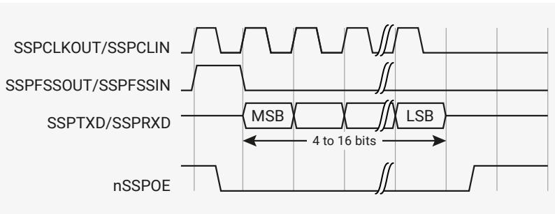
The diagram shows four signals over time: SSPCLKOUT/SSPCLIN , SSPFSSOUT/SSPFSSIN , SSPTXD/SSPRXD , and nSSPOE . SSPCLKOUT/SSPCLIN is a periodic square wave. SSPFSSOUT/SSPFSSIN is a single pulse that occurs at the rising edge of the first clock cycle. SSPTXD/SSPRXD shows a data frame of 4 to 16 bits, with the first bit labeled MSB and the last bit labeled LSB . nSSPOE is a signal that is active-low, going low at the start of the frame and returning high after the frame is complete.
In this mode, SSPCLKOUT and SSPFSSOUT are forced LOW, and the transmit data line, SSPTXD is tristated whenever the PrimeCell SSP is idle. When the bottom entry of the transmit FIFO contains data, SSPFSSOUT is pulsed HIGH for one SSPCLKOUT period. The value to be transmitted is also transferred from the transmit FIFO to the serial shift register of the transmit logic. On the next rising edge of SSPCLKOUT , the MSB of the 4-bit to 16-bit data frame is shifted out on the SSPTXD pin. In a similar way, the MSB of the received data is shifted onto the SSPRXD pin by the off-chip serial slave device.
Both the PrimeCell SSP and the off-chip serial slave device then clock each data bit into their serial shifter on the falling edge of each SSPCLKOUT . The received data is transferred from the serial shifter to the receive FIFO on the first rising edge of CLK after the LSB has been latched.
Figure 93 shows the Texas Instruments synchronous serial frame format when back-to-back frames are transmitted.
Figure 93. Texas Instruments synchronous serial frame format, continuous transfer
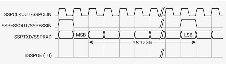
The diagram shows four signals over time: SSPCLKOUT/SSPCLIN , SSPFSSOUT/SSPFSSIN , SSPTXD/SSPRXD , and nSSPOE (=0) . SSPCLKOUT/SSPCLIN is a periodic square wave. SSPFSSOUT/SSPFSSIN is a single pulse that occurs at the rising edge of the first clock cycle. SSPTXD/SSPRXD shows a data frame of 4 to 16 bits, with the first bit labeled MSB and the last bit labeled LSB . nSSPOE (=0) is a signal that is active-low, going low at the start of the frame and returning high after the frame is complete.
12.3.4.9. Motorola SPI frame format
The Motorola SPI interface is a four-wire interface where the SSPFSSOUT signal behaves as a slave select. The main feature of the Motorola SPI format is that you can program the inactive state and phase of the SSPCLKOUT signal using the SP0 and SPH bits of the SSPSCR0 control register.
12.3.4.9.1. SP0, clock polarity
When the SP0 clock polarity control bit is LOW, it produces a steady state LOW value on the SSPCLKOUT pin. If the SP0 clock polarity control bit is HIGH, a steady state HIGH value is placed on the SSPCLKOUT pin when data is not being transferred.
12.3.4.9.2. SPH, clock phase
The SPH control bit selects the clock edge that captures data and enables it to change state. It has the most impact on the first bit transmitted by either permitting or not permitting a clock transition before the first data capture edge.
When the SPH phase control bit is LOW, data is captured on the first clock edge transition.
When the SPH clock phase control bit is HIGH, data is captured on the second clock edge transition.
12.3.4.10. Motorola SPI format with SP0=0, SPH=0
Figure 94 and Figure 95 shows a continuous transmission signal sequence for Motorola SPI frame format with SP0=0 , SPH=0 . Figure 94 shows a single transmission signal sequence for Motorola SPI frame format with SP0=0 , SPH=0 .
Figure 94. Motorola SPI frame format, single transfer, with SP0=0 and SPH=0
Figure 95 shows a continuous transmission signal sequence for Motorola SPI frame format with SP0=0 , SPH=0 .
Figure 95. Motorola SPI frame format, single transfer, with SP0=0 and SPH=0
In this configuration, during idle periods:
- • the SSPCLKOUT signal is forced LOW
- • the SSPFSSOUT signal is forced HIGH
- • the transmit data line SSPTXD is arbitrarily forced LOW
- • the nSSPOE pad enable signal is forced HIGH (this is not connected to the pad in RP2350)
- • when the PrimeCell SSP is configured as a master, the nSSPCTL0E line is driven LOW, enabling the SSPCLKOUT pad, active-LOW enable
- • when the PrimeCell SSP is configured as a slave, the nSSPCTL0E line is driven HIGH, disabling the SSPCLKOUT pad, active-LOW enable
If the PrimeCell SSP is enable, and there is valid data within the transmit FIFO, the start of transmission is signified by the SSPFSSOUT master signal being driven LOW. This causes slave data to be enabled onto the SSPRXD input line of the master. The nSSPOE line is driven LOW, enabling the master SSPTXD output pad.
One-half SSPCLKOUT period later, valid master data is transferred to the SSPTXD pin. Now that both the master and slave data have been set, the SSPCLKOUT master clock pin goes HIGH after one additional half SSPCLKOUT period.
The data is now captured on the rising and propagated on the falling edges of the SSPCLKOUT signal.
In the case of a single word transmission, after all bits of the data word have been transferred, the SSPFSSOUT line is returned to its idle HIGH state one SSPCLKOUT period after the last bit has been captured.
However, in the case of continuous back-to-back transmissions, the SSPFSSOUT signal pulse HIGH between each data word transfer. This is because the slave select pin freezes the data in its serial peripheral register and does not permit it to be altered if the SPH bit is logic zero. Therefore, the master device must raise the SSPFSSIN pin of the slave device between each data transfer to enable the serial peripheral data write. On completion of the continuous transfer, the SSPFSSOUT pin is returned to its idle state one SSPCLKOUT period after the last bit has been captured.
12.3.4.11. Motorola SPI format with SPO=0, SPH=1
Figure 96 shows the transfer signal sequence for Motorola SPI format with SPO=0 , SPH=1 , and it covers both single and continuous transfers.
Figure 96. Motorola SPI frame format with SPO=0 and SPH=1, single and continuous transfers
In this configuration, during idle periods:
- the SSPCLKOUT signal is forced LOW
- The SSPFSSOUT signal is forced HIGH
- the transmit data line SSPTXD is arbitrarily forced LOW
- the nSSPOE pad enable signal is forced HIGH (not connected to the pad in RP2350)
- when the PrimeCell SSP is configured as a master, the nSSPCTL0E line is driven LOW, enabling the SSPCLKOUT pad, active-LOW enable
- when the PrimeCell SSP is configured as a slave, the nSSPCTL0E line is driven HIGH, disabling the SSPCLKOUT pad, active-LOW enable
If the PrimeCell SSP is enabled, and there is valid data within the transmit FIFO, the start of transmission is signified by the SSPFSSOUT master signal being driven LOW. The nSSPOE line is driven LOW, enabling the master SSPTXD output pad. After an additional one half SSPCLKOUT period, both master and slave valid data is enabled onto their respective transmission lines. At the same time, the SSPCLKOUT is enabled with a rising edge transition.
Data is then captured on the falling edges and propagated on the rising edges of the SSPCLKOUT signal.
In the case of a single word transfer, after all bits have been transferred, the SSPFSSOUT line is returned to its idle HIGH state one SSPCLKOUT period after the last bit has been captured. For continuous back-to-back transfers, the SSPFSSOUT pin is held LOW between successive data words and termination is the same as that of the single word transfer.
12.3.4.12. Motorola SPI format with SPO=1, SPH=0
Figure 97 and Figure 98 show single and continuous transmission signal sequences for Motorola SPI format with SPO=1, SPH=0.
Figure 97 shows a single transmission signal sequence for Motorola SPI format with SPO=1, SPH=0.
Figure 97. Motorola SPI frame format, single transfer, with SPO=1 and SPH=0
Figure 98 shows a continuous transmission signal sequence for Motorola SPI format with SPO=1, SPH=0.
i NOTE
In Figure 97, Q is an undefined signal.
Figure 98. Motorola SPI frame format, continuous transfer, with SPO=1 and SPH=0
In this configuration, during idle periods:
- • the SSPCLKOUT signal is forced HIGH
- • the SSPFSSOUT signal is forced HIGH
- • the transmit data line SSPTXD is arbitrarily forced LOW
- • the nSSPOE pad enable signal is forced HIGH (not connected to the pad in RP2350)
- • when the PrimeCell SSP is configured as a master, the nSSPCTL0E line is driven LOW, enabling the SSPCLKOUT pad, active-LOW enable
- • when the PrimeCell SSP is configured as a slave, the nSSPCTL0E line is driven HIGH, disabling the SSPCLKOUT pad, active-LOW enable
If the PrimeCell SSP is enabled, and there is valid data within the transmit FIFO, the start of transmission is signified by the SSPFSSOUT master signal being driven LOW, and this causes slave data to be immediately transferred onto the SSPRXD line of the master. The nSSPOE line is driven LOW, enabling the master SSPTXD output pad.
One half period later, valid master data is transferred to the SSPTXD line. Now that both the master and slave data have been set, the SSPCLKOUT master clock pin becomes LOW after one additional half SSPCLKOUT period. This means that data is captured on the falling edges and be propagated on the rising edges of the SSPCLKOUT signal.
In the case of a single word transmission, after all bits of the data word are transferred, the SSPFSSOUT line is returned to its idle HIGH state one SSPCLKOUT period after the last bit has been captured.
However, in the case of continuous back-to-back transmissions, the SSPFSSOUT signal must be pulsed HIGH between each data word transfer. This is because the slave select pin freezes the data in its serial peripheral register and does not permit it to be altered if the SPH bit is logic zero. Therefore, the master device must raise the SSPFSSIN pin of the slave device between each data transfer to enable the serial peripheral data write. On completion of the continuous transfer, the SSPFSSOUT pin is returned to its idle state one SSPCLKOUT period after the last bit has been captured.
12.3.4.13. Motorola SPI format with SPO=1, SPH=1
Figure 99 shows the transfer signal sequence for Motorola SPI format with SPO=1, SPH=1, and it covers both single and continuous transfers.
Figure 99. Motorola SPI frame format with SPO=1 and SPH=1, single and continuous transfers
NOTE
In Figure 99, Q is an undefined signal.
In this configuration, during idle periods:
- • the SSPCLKOUT signal is forced HIGH
- • the SSPFSSOUT signal is forced HIGH
- • the transmit data line SSPTXD is arbitrarily forced LOW
- • the nSSPOE pad enable signal is forced HIGH (not connected to the pad in RP2350)
- • when the PrimeCell SSP is configured as a master, the nSSPCTL0E line is driven LOW, enabling the SSPCLKOUT pad, active-LOW enable
- • when the PrimeCell SSP is configured as a slave, the nSSPCTL0E line is driven HIGH, disabling the SSPCLKOUT pad, active-LOW enable.
If the PrimeCell SSP is enabled, and there is valid data within the transmit FIFO, the start of transmission is signified by the SSPFSSOUT master signal being driven LOW. The nSSPOE line is driven LOW, enabling the master SSPTXD output pad. After an additional one half SSPCLKOUT period, both master and slave data are enabled onto their respective transmission lines. At the same time, the SSPCLKOUT is enabled with a falling edge transition. Data is then captured on the rising edges and propagated on the falling edges of the SSPCLKOUT signal.
After all bits have been transferred, in the case of a single word transmission, the SSPFSSOUT line is returned to its idle HIGH state one SSPCLKOUT period after the last bit has been captured.
For continuous back-to-back transmissions, the SSPFSSOUT pin remains in its active-LOW state, until the final bit of the last word has been captured, and then returns to its idle state as the previous section describes.
For continuous back-to-back transfers, the SSPFSSOUT pin is held LOW between successive data words and termination is the same as that of the single word transfer.
12.3.4.14. National Semiconductor Microwire frame format
Figure 100 shows the National Semiconductor Microwire frame format for a single frame. Figure 101 shows the same format when back to back frames are transmitted.
Figure 100. Microwire frame format, single transfer
Microwire format is very similar to SPI format, except that transmission is half-duplex instead of full-duplex, using a master-slave message passing technique. Each serial transmission begins with an 8-bit control word that is transmitted from the PrimeCell SSP to the off-chip slave device. During this transmission, the PrimeCell SSP receives no incoming data. After the message has been sent, the off-chip slave decodes it and, after waiting one serial clock after the last bit of the 8-bit control message has been sent, responds with the required data. The returned data is 4 to 16 bits in length, making the total frame length in the range 13-25 bits.
In this configuration, during idle periods:
- • SSPCLKOUT is forced LOW
- • SSPFSSOUT is forced HIGH
- • the transmit data line, SSPTXD , is arbitrarily forced LOW
- • the nSSPOE pad enable signal is forced HIGH (not connected to the pad in RP2350)
A transmission is triggered by writing a control byte to the transmit FIFO. The falling edge of SSPFSSOUT causes the value contained in the bottom entry of the transmit FIFO to be transferred to the serial shift register of the transmit logic, and the MSB of the 8-bit control frame to be shifted out onto the SSPTXD pin. SSPFSSOUT remains LOW for the duration of the frame transmission. The SSPRXD pin remains tristated during this transmission.
The off-chip serial slave device latches each control bit into its serial shifter on the rising edge of each SSPCLKOUT . After the last bit is latched by the slave device, the control byte is decoded during a one clock wait-state, and the slave responds by transmitting data back to the PrimeCell SSP. Each bit is driven onto SSPRXD line on the falling edge of SSPCLKOUT . The PrimeCell SSP in turn latches each bit on the rising edge of SSPCLKOUT . At the end of the frame, for single transfers, the SSPFSSOUT signal is pulled HIGH one clock period after the last bit has been latched in the receive serial shifter, that causes the data to be transferred to the receive FIFO.
NOTE
The off-chip slave device can tristate the receive line either on the falling edge of SSPCLKOUT after the LSB has been latched by the receive shifter, or when the SSPFSSOUT pin goes HIGH.
For continuous transfers, data transmission begins and ends in the same manner as a single transfer. However, the SSPFSSOUT line is continuously asserted, held LOW, and transmission of data occurs back-to-back. The control byte of the next frame follows directly after the LSB of the received data from the current frame. Each of the received values is transferred from the receive shifter on the falling edge SSPCLKOUT , after the LSB of the frame has been latched into the PrimeCell SSP.
Figure 101 shows the National Semiconductor Microwire frame format when back-to-back frames are transmitted.
Figure 101. Microwire frame format, continuous transfers
In Microwire mode, the PrimeCell SSP slave samples the first bit of receive data on the rising edge of SSPCLKIN after SSPFSSIN has gone LOW. Masters that drive a free-running SSPCLKIN must ensure that the SSPFSSIN signal has sufficient setup and hold margins with respect to the rising edge of SSPCLKIN .
Figure 102 shows these setup and hold time requirements.
Figure 104. PrimeCell SSP master coupled to an SPI slave
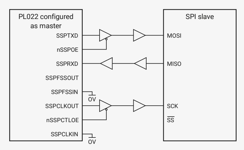
Figure 105 shows a Motorola SPI configured as a master and interfaced to an instance of a PrimeCell SSP (PL022) configured as a slave. In this case, the slave Select Signal ( \( \overline{SS} \) ) is permanently tied HIGH to configure it as a master. The master can broadcast to the slave through the master SPI MOSI line and in response, the slave drives its nSSPOE signal LOW. This enables its SSPTXD data onto the MISO line of the master.
Figure 105. SPI master coupled to a PrimeCell SSP slave
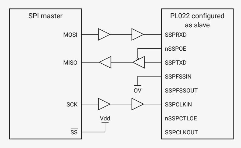
12.3.4.16. PrimeCell DMA interface
The PrimeCell SSP provides an interface to connect to the DMA controller. The PrimeCell SSP DMA control register, SSPDMACR controls the DMA operation of the PrimeCell SSP.
The DMA interface includes the following signals, for receive:
SSPRXDMASREQ
Single-character DMA transfer request, asserted by the SSP. This signal is asserted when the receive FIFO contains at least one character.
SSPRXDMABREQ
Burst DMA transfer request, asserted by the SSP. This signal is asserted when the receive FIFO contains four or more characters.
SSPRXDACLK
DMA request clear, asserted by the DMA controller to clear the receive request signals. If DMA burst transfer is requested, the clear signal is asserted during the transfer of the last data in the burst.
The DMA interface includes the following signals, for transmit:
SSPTXDMASREQ
Single-character DMA transfer request, asserted by the SSP. This signal is asserted when there is at least one empty location in the transmit FIFO.
SSPTXDMABREQ
Burst DMA transfer request, asserted by the SSP. This signal is asserted when the transmit FIFO contains four characters or fewer.
SSPTXDMACLR
DMA request clear, asserted by the DMA controller, to clear the transmit request signals. If a DMA burst transfer is requested, the clear signal is asserted during the transfer of the last data in the burst.
The burst transfer and single transfer request signals are not mutually exclusive. They can both be asserted at the same time. For example, when there is more data than the watermark level of four in the receive FIFO, the burst transfer request, and the single transfer request, are asserted. When the amount of data left in the receive FIFO is less than the watermark level, the single request only is asserted. This is useful for situations where the number of characters left to be received in the stream is less than a burst.
For example, if 19 characters must be received, the DMA controller then transfers four bursts of four characters, and three single transfers to complete the stream.
NOTE
For the remaining three characters, the PrimeCell SSP does not assert the burst request.
Each request signal remains asserted until the relevant DMA clear signal is asserted. After the request clear signal is de-asserted, a request signal can become active again, depending on the conditions that previous sections describe. All request signals are de-asserted if the PrimeCell SSP is disabled, or the DMA enable signal is cleared.
Table 1098 shows the trigger points for DMABREQ, for both the transmit and receive FIFOs.
Table 1098. DMA trigger points for the transmit and receive FIFOs
| Burst length | ||
|---|---|---|
| Watermark level | Transmit, number of empty locations | Receive, number of filled locations |
| 1/2 | 4 | 4 |
Figure 106 shows the timing diagram for both a single transfer request, and a burst transfer request, with the appropriate DMA clear signal. The signals are all synchronous to PCLK.
Figure 106. DMA transfer waveforms

The diagram shows four digital signals over time, synchronized to a PCLK clock. PCLK is a periodic square wave. DMASREQ (single transfer request) is asserted (goes high) at the start of a PCLK cycle and remains high until the end of the cycle. DMABREQ (burst transfer request) is asserted at the start of a PCLK cycle and remains high for multiple cycles. DMACLR (DMA request clear) is asserted at the end of a PCLK cycle and remains high for multiple cycles, clearing the DMASREQ and DMABREQ signals.
12.3.5. List of registers
The SPI0 and SPI1 registers start at base addresses of 0x40080000 and 0x40088000 respectively (defined as SPI0_BASE and SPI1_BASE in SDK).
Table 1099. List of SPI registers
| Offset | Name | Info |
|---|---|---|
| 0x000 | SSPCR0 | Control register 0, SSPCR0 on page 3-4 |
| 0x004 | SSPCR1 | Control register 1, SSPCR1 on page 3-5 |
| 0x008 | SSPDR | Data register, SSPDR on page 3-6 |
| 0x00c | SSPSR | Status register, SSPSR on page 3-7 |
| 0x010 | SSPCPSR | Clock prescale register, SSPCPSR on page 3-8 |
| Offset | Name | Info |
|---|---|---|
| 0x014 | SSPIMSC | Interrupt mask set or clear register, SSPIMSC on page 3-9 |
| 0x018 | SSPRIS | Raw interrupt status register, SSPRIS on page 3-10 |
| 0x01c | SSPMIS | Masked interrupt status register, SSPMIS on page 3-11 |
| 0x020 | SSPICR | Interrupt clear register, SSPICR on page 3-11 |
| 0x024 | SSPDMACR | DMA control register, SSPDMACR on page 3-12 |
| 0xfe0 | SSPPERIPHID0 | Peripheral identification registers, SSPPeriphID0-3 on page 3-13 |
| 0xfe4 | SSPPERIPHID1 | Peripheral identification registers, SSPPeriphID0-3 on page 3-13 |
| 0xfe8 | SSPPERIPHID2 | Peripheral identification registers, SSPPeriphID0-3 on page 3-13 |
| 0xfec | SSPPERIPHID3 | Peripheral identification registers, SSPPeriphID0-3 on page 3-13 |
| 0xff0 | SSPPCELLID0 | PrimeCell identification registers, SSPPCellID0-3 on page 3-16 |
| 0xff4 | SSPPCELLID1 | PrimeCell identification registers, SSPPCellID0-3 on page 3-16 |
| 0xff8 | SSPPCELLID2 | PrimeCell identification registers, SSPPCellID0-3 on page 3-16 |
| 0xffc | SSPPCELLID3 | PrimeCell identification registers, SSPPCellID0-3 on page 3-16 |
SPI: SSPCR0 Register
Offset: 0x000
Description
Control register 0, SSPCR0 on page 3-4
Table 1100. SSPCR0 Register
| Bits | Description | Type | Reset |
|---|---|---|---|
| 31:16 | Reserved. | - | - |
| 15:8 | SCR : Serial clock rate. The value SCR is used to generate the transmit and receive bit rate of the PrimeCell SSP. The bit rate is: \( F_{SSPCLK} \times \text{CPSDVSR} \times (1 + \text{SCR}) \) where CPSDVSR is an even value from 2-254, programmed through the SSPCPSR register and SCR is a value from 0-255. | RW | 0x00 |
| 7 | SPH : SSPCLKOUT phase, applicable to Motorola SPI frame format only. See Motorola SPI frame format on page 2-10. | RW | 0x0 |
| 6 | SPO : SSPCLKOUT polarity, applicable to Motorola SPI frame format only. See Motorola SPI frame format on page 2-10. | RW | 0x0 |
| 5:4 | FRF : Frame format: 00 Motorola SPI frame format. 01 TI synchronous serial frame format. 10 National Microwire frame format. 11 Reserved, undefined operation. | RW | 0x0 |
| 3:0 | DSS : Data Size Select: 0000 Reserved, undefined operation. 0001 Reserved, undefined operation. 0010 Reserved, undefined operation. 0011 4-bit data. 0100 5-bit data. 0101 6-bit data. 0110 7-bit data. 0111 8-bit data. 1000 9-bit data. 1001 10-bit data. 1010 11-bit data. 1011 12-bit data. 1100 13-bit data. 1101 14-bit data. 1110 15-bit data. 1111 16-bit data. | RW | 0x0 |
SPI: SSPCR1 Register
Offset: 0x004
Description
Control register 1, SSPCR1 on page 3-5
Table 1101. SSPCR1 Register
| Bits Register 31:21 20 19:16 15:12 11:0 | column_2 | Description ARCHITECT : Defines the architect of the component. Bits [31:28] are the PRESENT : Defines that the DEVARCH register is present REVISION : Defines the architecture revision of the component ARCHVER : Defines the architecture version of the component ARCHPART : Defines the architecture of the component | Type RO RO RO RO RO | Reset 0x23b 0x1 0x0 0x1 0xa02 |
|---|---|---|---|---|
| 31:4 | Reserved. | - | - | |
| 3 | SOD | : Slave-mode output disable. This bit is relevant only in the slave mode, slave drives data onto its serial output line. In such systems the RXD lines | RW | 0x0 |
| 2 | MS | not drive the SSPTXD output in slave mode. : Master or slave mode select. This bit can be modified only when the Device configured as slave. | RW | 0x0 |
| 1 | SSE | : Synchronous serial port enable: 0 SSP operation disabled. 1 SSP operation enabled. | RW | 0x0 |
| 0 | LBM | : Loop back mode: 0 Normal serial port operation enabled. 1 Output of | RW | 0x0 |
| Bits | Description | Type | Reset | |
| 31:16 | Reserved. | - | - | |
| 15:0 | DATA | : Transmit/Receive FIFO: Read Receive FIFO. Write Transmit FIFO. You The receive logic automatically right-justifies. | RWF | - |
| Bits | Description | Type | Reset | |
| 31:5 | Reserved. | - | - | |
| 4 | BSY | : PrimeCell SSP busy flag, RO: 0 SSP is idle. 1 SSP is currently transmitting and/or receiving a frame or the transmit FIFO is not empty. | RO | 0x0 |
| 3 | RFF | : Receive FIFO full, RO: 0 Receive FIFO is not full. 1 Receive FIFO is full. | RO | 0x0 |
| 2 | RNE | : Receive FIFO not empty, RO: 0 Receive FIFO is empty. 1 Receive FIFO is not empty. | RO | 0x0 |
| 1 | TNF full. | : Transmit FIFO not full, RO: 0 Transmit FIFO is full. 1 Transmit FIFO is not | RO | 0x1 |
| 0 | TFE | : Transmit FIFO empty, RO: 0 Transmit FIFO is not empty. 1 Transmit FIFO is empty. | RO | 0x1 |
SPI: SSPDR Register
Offset: 0x008
Description
Data register, SSPDR on page 3-6
Table 1102. SSPDR Register
SPI: SSPSR Register
Offset: 0x00c
Description
Status register, SSPSR on page 3-7
Table 1103. SSPSR Register
SPI: SSPCPSR Register
Offset: 0x010
Description
Clock prescale register, SSPCPSR on page 3-8
Table 1104. SSPCPSR Register
| Bits 23:16 15:8 7:0 Bits 31:24 | column_2 | Description ATTR2 : Memory attribute encoding for MPU regions with an AttrIndex of 2 ATTR1 : Memory attribute encoding for MPU regions with an AttrIndex of 1 ATTR0 : Memory attribute encoding for MPU regions with an AttrIndex of 0 Description ATTR7 : Memory attribute encoding for MPU regions with an AttrIndex of 7 | Type RW RW RW Type RW | Reset 0x00 0x00 0x00 Reset 0x00 | Description |
|---|---|---|---|---|---|
| 31:8 | Reserved. | - | - | Table 1104. SSPCPSR | |
| 7:0 | CPSDVSR | : Clock prescale divisor. Must be an even number from 2-254, depending on the frequency of SSPCLK. The least significant bit always returns zero on reads. | RW | 0x00 | Table 1104. SSPCPSR |
| Bits | Description | Type | Reset | Offset : 0x014 Description Interrupt mask set or clear register, SSPIMSC on page 3-9 Table 1105. SSPIMSC | |
| 31:4 | Reserved. | - | - | Register | |
| 3 | TXIM | : Transmit FIFO interrupt mask: 0 Transmit FIFO half empty or less condition interrupt is masked. 1 Transmit FIFO half empty or less condition interrupt is not masked. | RW | 0x0 | Register |
| 2 | RXIM | : Receive FIFO interrupt mask: 0 Receive FIFO half full or less condition masked. | RW | 0x0 | Register |
| 1 | RTIM | : Receive timeout interrupt mask: 0 Receive FIFO not empty and no read read prior to timeout period interrupt is not masked. | RW | 0x0 | Register |
| 0 | RORIM | : Receive overrun interrupt mask: 0 Receive FIFO written to while full condition interrupt is masked. 1 Receive FIFO written to while full condition interrupt is not masked. | RW | 0x0 | Register |
| Bits | Description | Type | Reset | Offset : 0x018 Description Raw interrupt status register, SSPRIS on page 3-10 Table 1106. SSPRIS | |
| 31:4 | Reserved. | - | - | Register | |
| 3 | TXRIS | : Gives the raw interrupt state, prior to masking, of the SSPTXINTR interrupt | RO | 0x1 | Register |
| 2 | RXRIS | : Gives the raw interrupt state, prior to masking, of the SSPRXINTR interrupt | RO | 0x0 | Register |
| 1 | RTRIS | : Gives the raw interrupt state, prior to masking, of the SSPRTINTR interrupt | RO | 0x0 | Register |
SPI: SSPIMSC Register
Offset: 0x014
Description
Interrupt mask set or clear register, SSPIMSC on page 3-9
Table 1105. SSPIMSC Register
SPI: SSPRIS Register
Offset: 0x018
Description
Raw interrupt status register, SSPRIS on page 3-10
Table 1106. SSPRIS Register
| Bits 2 1 0 Bits | Description RESET PUSH DATA Description | : Reset (before sending a new key) | Type RW RW RW Type | Reset 0x0 0x0 0x0 Reset |
|---|---|---|---|---|
| 31:4 | Reserved. | - | - | |
| 3 | TXMIS | : Gives the transmit FIFO masked interrupt state, after masking, of the | RO | 0x0 |
| 2 | RXMIS | SSPTXINTR interrupt : Gives the receive FIFO masked interrupt state, after masking, of the | RO | 0x0 |
| 1 | RTMIS | SSPRXINTR interrupt : Gives the receive timeout masked interrupt state, after masking, of the | RO | 0x0 |
| 0 | RORMIS | SSPRTINTR interrupt : Gives the receive over run masked interrupt status, after masking, of the SSPRORINTR interrupt | RO | 0x0 |
| Bits | Description | Type | Reset | |
| 31:2 | Reserved. | - | - | |
| 1 | RTIC | : Clears the SSPRTINTR interrupt | WC | 0x0 |
| 0 | RORIC | : Clears the SSPRORINTR interrupt SSPDMACR Register | WC | 0x0 |
| Bits | Description | Type | Reset | |
| 31:2 | Reserved. | - | - | |
| 1 | TXDMAE | : Transmit DMA Enable. If this bit is set to 1, DMA for the transmit | RW | 0x0 |
| 0 | RXDMAE | FIFO is enabled. : Receive DMA Enable. If this bit is set to 1, DMA for the receive FIFO is enabled. | RW | 0x0 |
SPI: SSPMIS Register
Offset: 0x01c
Description
Masked interrupt status register, SSPMIS on page 3-11
Table 1107. SSPMIS Register
SPI: SSPICR Register
Offset: 0x020
Description
Interrupt clear register, SSPICR on page 3-11
Table 1108. SSPICR Register
SPI: SSPDMACR Register
Offset: 0x024
Description
DMA control register, SSPDMACR on page 3-12
Table 1109. SSPDMACR Register
SPI: SSPPERIPHID0 Register
Offset: 0xfe0
Table 1114.
SSPPCELLID0 Register
| Bits | Description | Type | Reset |
|---|---|---|---|
| 31:8 | Reserved. | - | - |
| 7:0 | SSPPCELLID0 : These bits read back as 0x0D | RO | 0x0d |
SPI: SSPPCELLID1 Register
Offset: 0xff4
Description
PrimeCell identification registers, SSPPCellIID0-3 on page 3-16
Table 1115.
SSPPCELLID1 Register
| Bits | Description | Type | Reset |
|---|---|---|---|
| 31:8 | Reserved. | - | - |
| 7:0 | SSPPCELLID1 : These bits read back as 0xF0 | RO | 0xf0 |
SPI: SSPPCELLID2 Register
Offset: 0xff8
Description
PrimeCell identification registers, SSPPCellIID0-3 on page 3-16
Table 1116.
SSPPCELLID2 Register
| Bits | Description | Type | Reset |
|---|---|---|---|
| 31:8 | Reserved. | - | - |
| 7:0 | SSPPCELLID2 : These bits read back as 0x05 | RO | 0x05 |
SPI: SSPPCELLID3 Register
Offset: 0xffc
Description
PrimeCell identification registers, SSPPCellIID0-3 on page 3-16
Table 1117.
SSPPCELLID3 Register
| Bits | Description | Type | Reset |
|---|---|---|---|
| 31:8 | Reserved. | - | - |
| 7:0 | SSPPCELLID3 : These bits read back as 0xB1 | RO | 0xb1 |
12.4. ADC and Temperature Sensor
RP2350 has an internal analogue-digital converter (ADC) with the following features:
- • SAR ADC (see Section 12.4.3 )
- • 500 kS/s (using an independent 48 MHz clock)
- • 12-bit with 9.2 ENOB (see Section 12.4.4 )
- • Five or nine input mux:
- ◦ Four inputs available on QFN-60 package pins shared with GPIO[29:26]
- ◦ Eight inputs available on QFN-80 package pins shared with GPIO[47:40]
- ◦ One input dedicated to the internal temperature sensor (see Section 12.4.6 )
- • Eight element receive sample FIFO
- • Interrupt generation
- • DMA interface (see Section 12.4.3.5 )
Figure 107 shows the arrangement of ADC channels in the QFN-60 package. Figure 108 shows the same for QFN-80.
Figure 107. ADC Connection Diagram for QFN-60. This package features four external ADC inputs (0 through 3), on Bank 0 GPIOs 26 through 29. The internal temperature sensor connects to a fifth channel (channel 4). This is functionally the same ADC arrangement as RP2040, although the underlying hardware is different, to support the additional channels on QFN-80.
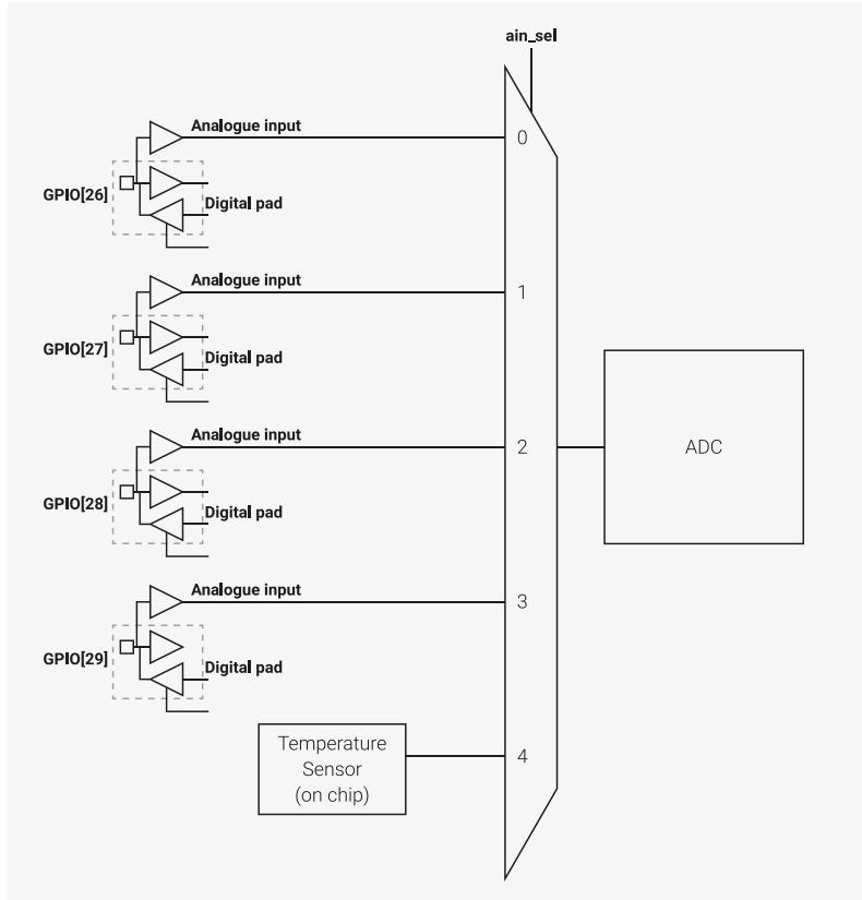
The diagram illustrates the ADC connection for the QFN-60 package. It shows four external ADC inputs (0 through 3) connected to Bank 0 GPIOs 26 through 29. Each input is connected to an 'Analogue input' and a 'Digital pad'. The internal temperature sensor connects to channel 4. The ADC block is connected to the 'ain_sel' bus, which selects the input for the ADC.
graph LR
    subgraph GPIOs [Bank 0 GPIOs]
        direction TB
        GPIO26[GPIO[26]]
        GPIO27[GPIO[27]]
        GPIO28[GPIO[28]]
        GPIO29[GPIO[29]]
    end

    subgraph Inputs [ADC Inputs]
        direction TB
        AI0[Analogue input 0]
        AI1[Analogue input 1]
        AI2[Analogue input 2]
        AI3[Analogue input 3]
        AI4[Analogue input 4]
    end

    subgraph Pads [Digital pads]
        direction TB
        DP0[Digital pad 0]
        DP1[Digital pad 1]
        DP2[Digital pad 2]
        DP3[Digital pad 3]
    end

    subgraph Sensors [Sensors]
        direction TB
        TS[Temperature Sensor on chip]
    end

    subgraph ADC [ADC]
        direction TB
        AI0 --- ADC
        AI1 --- ADC
        AI2 --- ADC
        AI3 --- ADC
        AI4 --- ADC
    end

    GPIO26 --- AI0
    GPIO26 --- DP0
    GPIO27 --- AI1
    GPIO27 --- DP1
    GPIO28 --- AI2
    GPIO28 --- DP2
    GPIO29 --- AI3
    GPIO29 --- DP3
    TS --- AI4

    AI0 --- ain_sel[ain_sel 0]
    AI1 --- ain_sel[ain_sel 1]
    AI2 --- ain_sel[ain_sel 2]
    AI3 --- ain_sel[ain_sel 3]
    AI4 --- ain_sel[ain_sel 4]
Figure 108. ADC Connection Diagram for QFN-80. This package features eight external ADC inputs (0 through 7), on Bank 0 GPIOs 40 through 47. The internal temperature sensor connects to a ninth channel (channel 8). Like in QFN-60, each ADC input shares a package pin with a digital Bank 0 GPIO: generally the digital functions are disabled when the ADC is in use.
![ADC Connection Diagram for QFN-80. The diagram shows a vertical bus labeled 'ain_sel' with pins 0 through 8. Pins 0-7 are connected to external ADC inputs, each sharing a package pin with a digital Bank 0 GPIO (GPIO[40] through GPIO[47]). Each input has an 'Analogue input' and a 'Digital pad' (indicated by a dashed box). Pin 8 is connected to an internal 'Temperature Sensor (on chip)'. A block labeled 'ADC' is connected to the bus between pins 4 and 5.](/RP235x/6280286fa7814c1ff5621a296b5854f8_img.jpg)
The diagram illustrates the ADC connection for the QFN-80 package. It features a vertical bus labeled 'ain_sel' with pins 0 through 8. Pins 0 through 7 are connected to external ADC inputs, each sharing a package pin with a digital Bank 0 GPIO (GPIO[40] through GPIO[47]). Each input has an 'Analogue input' and a 'Digital pad' (indicated by a dashed box). Pin 8 is connected to an internal 'Temperature Sensor (on chip)'. A block labeled 'ADC' is connected to the bus between pins 4 and 5.
When using an ADC input shared with a GPIO pin, always disable the pin’s digital functions by setting IE low and OD high in the pin’s pad control register. See Section 9.11.3, “Pad Control - User Bank” for details.
The maximum ADC input voltage is determined by the digital IO supply voltage ( IOVDD ), not the ADC supply voltage ( ADC_AVDD ). For example, if IOVDD is powered at 1.8 V, the voltage on the ADC inputs should not exceed 1.8 V + 10% even if ADC_AVDD is powered at 3.3 V. Voltages greater than IOVDD will result in leakage currents through the ESD protection diodes. See Section 14.9, “Electrical specifications” for details.
12.4.1. Changes from RP2040
- Removed spikes in differential nonlinearity at codes 0x200 , 0x600 , 0xa00 and 0xe00 , as documented by erratum RP2040-E11, improving the ADC’s precision by around 0.5 ENOB.
- • Increased the number of external ADC input channels from 4 to 8 channels, in the QFN-80 package only.
12.4.2. ADC controller
A digital controller manages the details of operating the RP2350 ADC, and provides additional functionality:
- • One-shot or free-running capture mode
- • Sample FIFO with DMA interface
- • Pacing timer (16 integer bits, 8 fractional bits) for setting free-running sample rate
- • Round-robin sampling of multiple channels in free-running capture mode
- • Optional right-shift to 8 bits in free-running capture mode, so samples can be DMA'd to a byte buffer in system memory
12.4.2.1. Channel connections
The ADC channels are connected to the following GPIOs in QFN-60
Table 1118. ADC channel connections on QFN-60
| Channel | Connection |
|---|---|
| 0 | GPIO[26] |
| 1 | GPIO[27] |
| 2 | GPIO[28] |
| 3 | GPIO[29] |
| 4 | Temperature Sensor |
The ADC channels are connected to the following GPIOs in QFN-80
Table 1119. ADC channel connections on QFN-80
| Channel | Connection |
|---|---|
| 0 | GPIO[40] |
| 1 | GPIO[41] |
| 2 | GPIO[42] |
| 3 | GPIO[43] |
| 4 | GPIO[44] |
| 5 | GPIO[45] |
| 6 | GPIO[46] |
| 7 | GPIO[47] |
| 8 | Temperature Sensor |
12.4.3. SAR ADC
The Successive Approximation Register Analogue to Digital Converter (SAR ADC) is a combination of digital controller and analogue circuit as shown in Figure 109 and Figure 110 .
Figure 109. SAR ADC
Block diagram QFN-60
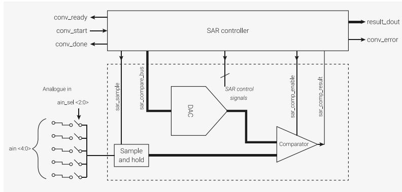
Figure 110. SAR ADC
Block diagram QFN-80
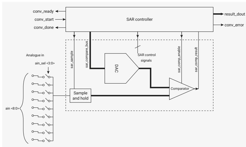
The ADC requires a 48 MHz clock (
clk_adc
), which could come from the USB PLL. Capturing a sample takes 96 clock cycles (
\(
96 \times 1/48 \text{ MHz} = 2 \mu\text{s}
\)
per sample (500 kS/s). The clock must be set up correctly before enabling the ADC.
When the ADC block is provided with a clock, and its reset has been removed, writing a 1 to
CS.EN
will start a short internal power-up sequence for the ADC's analogue hardware. After a few clock cycles,
CS.READY
will go high, indicating the ADC is ready to start its first conversion.
To save power, you can disable the ADC at any time by clearing
CS.EN
.
CS.EN
does
not
enable the temperature sensor bias source; it is controlled separately, see
Section 12.4.6
for details.
The ADC input is capacitive. When sampling, the ADC places about 1pF across the input. Packaging, PCB routing, and other external factors introduce additional capacitance. The effective impedance, even when sampling at 500 kS/s, is over 100 kΩ. DC measurements have no need to buffer.
12.4.3.1. One-shot sample
To select an ADC input, write to
CS.AINSEL
:
- On QFN-60, there are 4 external inputs, with an
AINSELvalue of 0 → 3 mapping to the ADC input on GPIO26 → GPIO29. SetAINSELto 4 to select the internal temperature sensor. - On QFN-80, there are 8 external inputs, with an
AINSELvalue of 0 → 7 mapping to the ADC input on GPIO40 → GPIO47. SetAINSELto 8 to select the internal temperature sensor.
Switching
AINSEL
requires no settling time.
Write a 1 to
CS.START_ONCE
to immediately start a new conversion.
CS.READY
will go low to show that a conversion is currently in progress. After 96 cycles of
clk_adc
,
CS.READY
will go high. The 12-bit conversion result is available in
RESULT
.
12.4.3.2. Free-running sampling
When
CS.START_MANY
is set, the ADC automatically starts new conversions at regular intervals. The most recent conversion result is always available in
RESULT
, but for IRQ or DMA-driven streaming of samples, you must enable the ADC FIFO (Section 12.4.3.4).
By default (
DIV = 0
), new conversions start immediately after the previous conversion finishes, producing a new sample every 96 cycles. At a clock frequency of 48 MHz, this produces 500 kS/s.
Set
DIV.INT
to a positive value
n
to trigger the ADC once per
n + 1
cycles. The ADC ignores this if a conversion is currently in progress, so generally
n
will be
\(
\geq 96
\)
. For example, setting
DIV.INT
to 47999 runs the ADC at 1 kS/s, if running from a 48 MHz clock.
The pacing timer supports fractional-rate division (first order delta sigma). When setting
DIV.FRAC
to a non-zero value, the ADC starts a new conversion once per
\(
1 + \text{INT} + \frac{\text{FRAC}}{256}
\)
cycles on average, by changing the sample interval between
INT + 1
and
INT + 2
.
12.4.3.3. Sampling multiple inputs
CS.RROBIN
allows the ADC to sample multiple inputs in an interleaved fashion while performing free-running sampling. Each bit in
RROBIN
corresponds to one of the five possible values of
CS.AINSEL
. When the ADC completes a conversion,
CS.AINSEL
automatically cycles to the next input whose corresponding bit is set in
RROBIN
.
To disable the round-robin sampling feature, write all-zeroes to
CS.RROBIN
.
For example, if
AINSEL
is initially 0, and
RROBIN
is set to
0x06
(bits 1 and 2 are set), the ADC samples channels in the following order:
- 1. Channel 0
- 2. Channel 1
- 3. Channel 2
- 4. Channel 1
- 5. Channel 2
- 6. Channel 1
- 7. Channel 2
The ADC continues to sample channels 1 and 2 indefinitely.
i NOTE
The initial value of
AINSEL
does not need to correspond with a set bit in
RROBIN
.
12.4.3.4. Sample FIFO
You can read ADC samples directly from the
RESULT
register or store them in a local 8-entry FIFO and read out from
FIFO
. Use the
FCS
register to control FIFO operation.
When
FCS.EN
is set, the ADC writes each conversion result to the FIFO. A software interrupt handler or the RP2350 DMA can read this sample from the FIFO when notified by the ADC's
IRQ
or
DREQ
signals. Alternatively, software can poll the status bits in
FCS
to wait for each sample to become available.
If the FIFO is full when a conversion completes, the sticky error flag
FCS.OVER
is set. When the FIFO is full, the current FIFO contents do not change, so any conversions that complete during this time are lost.
Two flags control the data written to the FIFO by the ADC:
- • FCS.SHIFT right-shifts the FIFO data to eight bits in size (i.e. FIFO bits 7:0 are conversion result bits 11:4). This is suitable for 8-bit DMA transfer to a byte buffer in memory, allowing deeper capture buffers, at the cost of some precision.
- • FCS.ERR sets the FIFO.ERR flag of each FIFO value, showing that a conversion error took place, i.e. the SAR failed to converge.
Conversion errors indicate that the comparison of one or more bits failed to complete in the time allowed. Conversion errors are typically caused by comparator metastability: the closer to the comparator threshold the input signal is, the longer it takes to make a decision. The higher the comparator gain, the lower the probability of conversion errors.
 CAUTION
Because conversion errors produce undefined results, you should always discard samples that contain conversion errors.
12.4.3.5. DMA
The RP2350 DMA (Section 12.6) can fetch ADC samples from the sample FIFO, by performing a normal memory-mapped read on the FIFO register, paced by the ADC_DREQ system data request signal. Before you can use the DMA to fetch ADC samples, you must:
- • Enable the sample FIFO ( FCS.EN ) so that samples are written to it; the FIFO is disabled by default so that it does not inadvertently fill when the ADC is used for one-shot conversions. Configure the ADC sample rate (Section 12.4.3.2) before starting the ADC.
- • Enable the ADC's data request handshake ( DREQ ) via FCS.DREQ_EN .
- • In the DMA channel used for the transfer, select the DREQ_ADC data request signal (Section 12.6.4.1).
- • Set the threshold for DREQ assertion ( FCS.THRESH ) to 1, so that the DMA transfers as soon as a single sample is present in the FIFO. This is also the threshold used for IRQ assertion, so non-DMA use cases might prefer a higher value for less frequent interrupts.
- • If the DMA transfer size is set to 8 bits (so that the DMA transfers to a byte array in memory), set FCS.SHIFT to pre-shift the FIFO samples to 8 bits of significance.
- • To sample multiple input channels, write a mask of those channels to CS.RROBIN . Additionally, select the first channel to sample with CS.AINSEL .
Once the ADC is suitably configured, start the DMA channel first, then the ADC conversion via CS.START_MANY . Once the DMA completes, you can halt the ADC if you are finished sampling, or promptly start a new DMA transfer before the FIFO fills up. After clearing CS.START_MANY to halt the ADC, software should poll CS.READY to make sure the last conversion has finished, then drain any stray samples from the FIFO.
12.4.3.6. Interrupts
Use INTE to generate an interrupt when the FIFO level reaches a threshold defined in FCS.THRESH .
Use INTS to read the interrupt status. To clear the interrupt, drain the FIFO to a level lower than FCS.THRESH .
12.4.3.7. Supply
RP2350 separates the ADC supply out on its own pin to allow noise filtering.
12.4.4. ADC ENOB
ADC ENOB details are shown in Table 1438 .
12.4.5. INL and DNL
Details to follow.
12.4.6. Temperature sensor
The temperature sensor measures the \( V_{be} \) voltage of a biased bipolar diode, connected to the fifth ADC channel ( \( A_{INSEL}=4 \) ) on QFN-60 or the ninth ADC channel ( \( A_{INSEL}=8 \) ) on QFN-80. Typically, \( V_{be} = 0.706\text{ V} \) at \( 27\text{ }^{\circ}\text{C} \) , with a slope of \( -1.721\text{ mV per degree} \) . Therefore the temperature in \( ^{\circ}\text{C} \) can be approximated as follows:
As the \( V_{be} \) and the \( V_{be} \) slope can vary over the temperature range, and from device to device, some user calibration may be required if accurate measurements are required.
The temperature sensor's bias source must be enabled before use, via CS.TS_EN . This increases current consumption on ADC_AVDD by approximately \( 40\text{ }\mu\text{A} \) .
The on board temperature sensor is very sensitive to errors in reference voltage. At \( 3.3\text{ V} \) , a value of 891 returned by the ADC corresponds to a temperature of \( 20.1^{\circ}\text{C} \) . At a reference voltage 1% lower than \( 3.3\text{ V} \) , the same reading of 891 correspond to a temperature of \( 24.3^{\circ}\text{C} \) : a temperature change of over \( 4^{\circ}\text{C} \) . To improve the accuracy of the internal temperature sensor, consider adding an external reference voltage.
12.4.7. List of registers
The ADC registers start at a base address of
0x400a0000
(defined as
ADC_BASE
in SDK).
Table 1120. List of ADC registers
| Offset 0x42fc8 0x42fcc 0x42fd0 0x42fd4 0x42fd8 | Name DEVID DEVTYPE PIDR4 PIDR5 PIDR6 | Info Device Configuration register Device Type Identifier register CoreSight Periperal ID4 CoreSight Periperal ID5 CoreSight Periperal ID6 |
|---|---|---|
| The temperature sensor measures the | Vbe voltage of a biased bipolar diode, connected to the fifth ADC channel ( | |
| AINSEL | =4) on QFN-60 or the ninth ADC channel ( | AINSEL =8) on QFN-80. Typically, Vbe = 0.706 V at 27 °C, with a slope of |
| As the | Vbe and the Vbe be required if accurate measurements are required. | slope can vary over the temperature range, and from device to device, some user calibration may |
| The temperature sensor’s bias source must be enabled before use, via CS .TS_EN. This increases current consumption | ||
| on ADC_AVDD NOTE | by approximately 40 μA. | |
| 12.4.7. List of registers The ADC registers start at a base address of | 0x400a0000 (defined as ADC_BASE in SDK). | |
| Offset ADC registers | Name | Info |
| 0x00 | CS | ADC Control and Status |
| 0x04 | RESULT | Result of most recent ADC conversion |
| 0x08 | FCS | FIFO control and status |
| 0x0c | FIFO | Conversion result FIFO |
| 0x10 | DIV | Clock divider. If non-zero, CS_START_MANY will start conversions |
| 0x14 | INTR | Total period is 1 + INT + FRAC / 256 Raw Interrupts |
| 0x18 | INTE | Interrupt Enable |
| 0x1c | INTF | Interrupt Force |
| 0x20 | INTS | Interrupt status after masking & forcing |
| 12.4. ADC and Temperature Sensor 12.4. ADC and Temperature Sensor | 1073 |
ADC: CS Register
Offset: 0x00
Description
ADC Control and Status
Table 1121. CS Register
| Bits 31:0 Bits 31:0 Bits 31:28 | column_2 | Description Description Input value for GPIO0…31. Description QSPI_SD : Input value on QSPI SD0 (MOSI), SD1 (MISO), SD2 and SD3 pins | Type RO Type RO Type RO | Reset - Reset 0x00000000 Reset 0x0 |
|---|---|---|---|---|
| 31:25 | Reserved. | - | - | |
| 24:16 | RROBIN | : Round-robin sampling. 1 bit per channel. Set all bits to 0 to disable. fashion. | RW | 0x000 |
| 15:12 | AINSEL | : Select analog mux input. Updated automatically in round-robin mode. This is corrected for the package option so only ADC channels which are bonded are available, and in the correct order | RW | 0x0 |
| 11 | Reserved. | - | - | |
| 10 | ERR_STICKY clear. | : Some past ADC conversion encountered an error. Write 1 to | WC | 0x0 |
| 9 | ERR | : The most recent ADC conversion encountered an error; result is undefined or noisy. | RO | 0x0 |
| 8 | READY | : 1 if the ADC is ready to start a new conversion. Implies any previous conversion has completed. 0 whilst conversion in progress. | RO | 0x0 |
| 7:4 | Reserved. | - | - | |
| 3 | START_MANY | : Continuously perform conversions whilst this bit is 1. A new conversion will start immediately after the previous finishes. | RW | 0x0 |
| 2 | START_ONCE | : Start a single conversion. Self-clearing. Ignored if start_many is asserted. | SC | 0x0 |
| 1 | TS_EN | : Power on temperature sensor. 1 - enabled. 0 - disabled. | RW | 0x0 |
| 0 | EN : Power on ADC and enable its clock. | RW | 0x0 | |
| Bits | : 0x04 Description | Type | Reset | |
| 31:12 | Reserved. | - | - | |
| 11:0 | Result of most recent ADC conversion | RO | 0x000 |
ADC: RESULT Register
Offset: 0x04
Table 1122. RESULT Register
ADC: FCS Register
Offset: 0x08
Description
FIFO control and status
Table 1123. FCS Register
| Bits | Description | Type | Reset |
|---|---|---|---|
| 31:28 | Reserved. | - | - |
| 27:24 | THRESH : DREQ/IRQ asserted when level >= threshold | RW | 0x0 |
| 23:20 | Reserved. | - | - |
| 19:16 | LEVEL : The number of conversion results currently waiting in the FIFO | RO | 0x0 |
| 15:12 | Reserved. | - | - |
| 11 | OVER : 1 if the FIFO has been overflowed. Write 1 to clear. | WC | 0x0 |
| 10 | UNDER : 1 if the FIFO has been underflowed. Write 1 to clear. | WC | 0x0 |
| 9 | FULL | RO | 0x0 |
| 8 | EMPTY | RO | 0x0 |
| 7:4 | Reserved. | - | - |
| 3 | DREQ_EN : If 1: assert DMA requests when FIFO contains data | RW | 0x0 |
| 2 | ERR : If 1: conversion error bit appears in the FIFO alongside the result | RW | 0x0 |
| 1 | SHIFT : If 1: FIFO results are right-shifted to be one byte in size. Enables DMA to byte buffers. | RW | 0x0 |
| 0 | EN : If 1: write result to the FIFO after each conversion. | RW | 0x0 |
ADC: FIFO Register
Offset: 0x0c
Description
Conversion result FIFO
Table 1124. FIFO Register
| Bits | Description | Type | Reset |
|---|---|---|---|
| 31:16 | Reserved. | - | - |
| 15 | ERR : 1 if this particular sample experienced a conversion error. Remains in the same location if the sample is shifted. | RF | - |
| 14:12 | Reserved. | - | - |
| 11:0 | VAL | RF | - |
ADC: DIV Register
Offset: 0x10
Description
Clock divider. If non-zero, CS_START_MANY will start conversions at regular intervals rather than back-to-back.
The divider is reset when either of these fields are written.
Total period is 1 + INT + FRAC / 256
Table 1125. DIV Register
| Bits | Description | Type | Reset |
|---|---|---|---|
| 31:24 | Reserved. | - | - |
| 23:8 | INT : Integer part of clock divisor. | RW | 0x0000 |
| 7:0 | FRAC : Fractional part of clock divisor. First-order delta-sigma. | RW | 0x00 |
ADC: INTR Register
Offset: 0x14
Description
Raw Interrupts
Table 1126. INTR Register
| Bits | Description | Type | Reset |
|---|---|---|---|
| 31:1 | Reserved. | - | - |
| 0 | FIFO:
Triggered when the sample FIFO reaches a certain level. This level can be programmed via the FCS_THRESH field. | RO | 0x0 |
ADC: INTE Register
Offset: 0x18
Description
Interrupt Enable
Table 1127. INTE Register
| Bits | Description | Type | Reset |
|---|---|---|---|
| 31:1 | Reserved. | - | - |
| 0 | FIFO:
Triggered when the sample FIFO reaches a certain level. This level can be programmed via the FCS_THRESH field. | RW | 0x0 |
ADC: INTF Register
Offset: 0x1c
Description
Interrupt Force
Table 1128. INTF Register
| Bits | Description | Type | Reset |
|---|---|---|---|
| 31:1 | Reserved. | - | - |
| 0 | FIFO:
Triggered when the sample FIFO reaches a certain level. This level can be programmed via the FCS_THRESH field. | RW | 0x0 |
ADC: INTS Register
Offset: 0x20
Description
Interrupt status after masking & forcing
Table 1129. INTS Register
| Bits | Description | Type | Reset |
|---|---|---|---|
| 31:1 | Reserved. | - | - |
| 0 | FIFO:
Triggered when the sample FIFO reaches a certain level. This level can be programmed via the FCS_THRESH field. | RO | 0x0 |
12.5. PWM
12.5.1. Overview
Pulse width modulation (PWM) smoothly varies the average voltage of a digital signal using controlled-width positive pulses at regular intervals. The fraction of time spent high is known as the duty cycle. This may be used to approximate an analogue output or control switchmode power electronics.
The RP2350 PWM block has 12 identical slices. Each slice can drive two PWM output signals, or measure the frequency or duty cycle of an input signal. The two outputs on each slice have the same period, but independently varying duty cycles, so this gives a total of 24 controllable PWM outputs in the QFN-80 package.
Figure 111. A single PWM slice. A 16-bit counter counts from 0 up to some programmed value, and then wraps to zero, or counts back down again, depending on PWM mode. The A and B outputs transition high and low based on the current count value and the preprogrammed A and B thresholds. The counter advances based on a number of events: it may be free-running, or gated by level or edge of an input signal on the B pin. A fractional divider slows the overall count rate for finer control of output frequency.
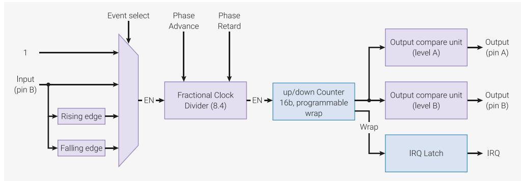
Each PWM slice is equipped with the following:
- • 16-bit counter
- • 8.4 fractional clock divider
- • Two independent output channels, duty cycle from 0% to 100% inclusive
- • Dual slope and trailing edge modulation
- • Edge-sensitive input mode for frequency measurement
- • Level-sensitive input mode for duty cycle measurement
- • Configurable counter wrap value
- ◦ Wrap and level registers are double buffered and can be changed race-free while PWM is running
- • Interrupt request and DMA request on counter wrap
- • Phase can be precisely advanced or retarded while running (increments of one count)
Slices can be enabled or disabled simultaneously via a single global control register. Slices then run in lockstep, so that more complex power circuitry can be switched by the outputs of multiple slices.
12.5.1.1. Changes from RP2040
- • Increased the number of slices from 8 to 12, with the 4 additional slices available on GPIOs 32 through 47 in the QFN-80 package.
- • Added a second shared interrupt line (controlled by IRQ1_INTE ), to aid use of PWM slices as simple repeating timers.
12.5.2. Programmer's model
All GPIO pins on RP2350 can be used for PWM:
Table 1130. Mapping of PWM channels to GPIO pins on RP2350. This is also shown in the main GPIO function table, Table 646
| GPIO | 0 | 1 | 2 | 3 | 4 | 5 | 6 | 7 | 8 | 9 | 10 | 11 | 12 | 13 | 14 | 15 |
| PWM Channel | 0A | 0B | 1A | 1B | 2A | 2B | 3A | 3B | 4A | 4B | 5A | 5B | 6A | 6B | 7A | 7B |
| GPIO | 16 | 17 | 18 | 19 | 20 | 21 | 22 | 23 | 24 | 25 | 26 | 27 | 28 | 29 | 30 | 31 |
| PWM Channel | 0A | 0B | 1A | 1B | 2A | 2B | 3A | 3B | 4A | 4B | 5A | 5B | 6A | 6B | 7A | 7B |
| GPIO | 32 | 33 | 34 | 35 | 36 | 37 | 38 | 39 | 40 | 41 | 42 | 43 | 44 | 45 | 46 | 47 |
| PWM Channel | 8A | 8B | 9A | 9B | 10A | 10B | 11A | 11B | 8A | 8B | 9A | 9B | 10A | 10B | 11A | 11B |
- • The first 16 PWM channels (8 × 2-channel slices) appear on GPIOs 0 through 15, in the order PWM0 A , PWM0 B , PWM1 A , and so on.
- • This pattern repeats for GPIOs 16 through 31. GPIO16 is PWM0 A , GPIO17 is PWM0 B , and so on up to PWM7 B on GPIO31. GPIO30 and above are available only in the QFN-80 package.
- • The remaining 8 PWM channels (4 × 2-channel slices) appear on GPIOs 32 through 39, and then repeat on GPIOs 40 through 47.
- • If you select the same PWM output on two GPIO pins, the same signal appears on both.
- • If you use B pin as an input and select it on multiple GPIO pins, the PWM slice sees the logical OR of those two GPIO inputs.
NOTE
GPIOs 0 through 29 have the same channel assignment as RP2040 for pinout compatibility. This reduces the maximum number of independent PWM outputs in the QFN-60 package option of RP2350, but you can still use slices 8 through 11 for repeating timer interrupts in this package.
12.5.2.1. Pulse width modulation (PWM)
The PWM hardware continuously compares an input value to a free-running counter. This produces a toggling output; the amount of time spent at the high output level corresponds to the input value. The fraction of time spent at the high signal level is known as the duty cycle of the signal.
The counting period is controlled by the TOP register, with a maximum possible period of 65536 cycles, as the counter and TOP are 16 bits in size. Use the CC register to configure input values.
Figure 112. The counter repeatedly counts from 0 to TOP, forming a sawtooth shape. The counter is continuously compared with some input value. When the input value is higher than the counter, the output is driven high. Otherwise, the output is low. The output period \( T \) is defined by the TOP value of the counter, and how fast the counter is configured to count. The average output voltage, as a fraction of the IO power supply, is the input value divided by the counter period ( \( TOP + 1 \) )
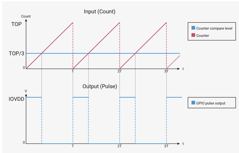
This example shows the counting period and the A and B counter compare levels being configured on one of RP2350's PWM slices.
Pico Examples: https://github.com/raspberrypi/pico-examples/blob/master/pwm/hello_pwm/hello_pwm.c Lines 14 - 29
14 // Tell GPIO 0 and 1 they are allocated to the PWM
15 gpio_set_function(0, GPIO_FUNC_PWM);
16 gpio_set_function(1, GPIO_FUNC_PWM);
17
18 // Find out which PWM slice is connected to GPIO 0 (it's slice 0)
19 uint slice_num = pwm_gpio_to_slice_num(0);
20
21 // Set period of 4 cycles (0 to 3 inclusive)
22 pwm_set_wrap(slice_num, 3);
23 // Set channel A output high for one cycle before dropping
24 pwm_set_chan_level(slice_num, PWM_CHAN_A, 1);
25 // Set initial B output high for three cycles before dropping
26 pwm_set_chan_level(slice_num, PWM_CHAN_B, 3);
27 // Set the PWM running
28 pwm_set_enabled(slice_num, true);
Figure 113 shows how the PWM hardware operates once it has been configured.
Figure 113. The slice counts repeatedly from 0 to 3, which is configured as the TOP value. The output waves therefore have a period of 4. Output A is high for 1 cycle in 4, so the average output voltage is 1/4 of the IO supply voltage. Output B is high for 3 cycles in every 4. The rising edges of A and B are always aligned.

By default, PWM slices count upward until they reach the value of the TOP register. After they reach the TOP value, they wrap to 0. Alternatively, set
CSR_PH_CORRECT
to 1 to enable
phase-correct mode
, where the counter counts downward after reaching TOP, until it reaches 0 again.
Phase-correct mode centres the pulse on the same point no matter the duty cycle; its phase is not a function of duty cycle. When phase-correct mode is enabled, the output frequency is halved. The slice spends two cycles at a count of TOP and two cycles at a count of 0 each PWM period.
Figure 114. In phase-correct mode, the counter counts back down from TOP to 0 once it reaches TOP.
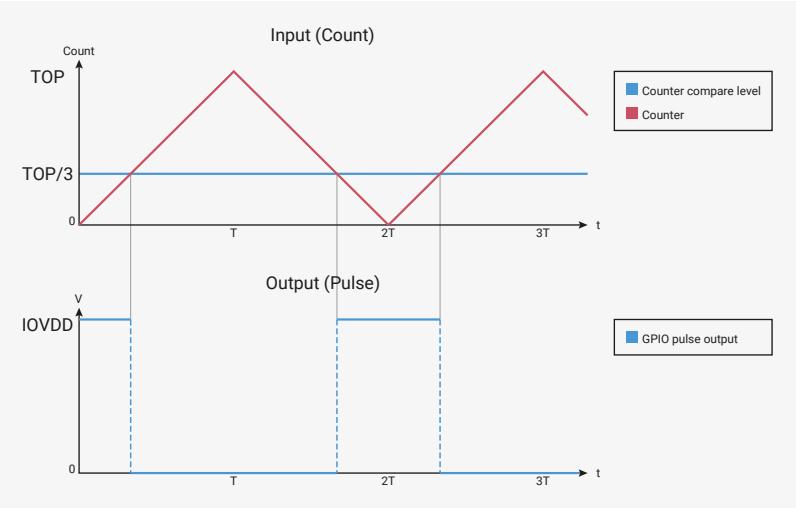
The diagram shows two vertically aligned plots sharing a common time axis \( t \) . The top plot, 'Input (Count)', has a vertical axis 'Count' with markers at 0, \( TOP/3 \) , and \( TOP \) . A red line represents the 'Counter', which increases linearly from 0 to \( TOP \) and then decreases linearly back to 0. A horizontal blue line at \( TOP/3 \) represents the 'Counter compare level'. The bottom plot, 'Output (Pulse)', has a vertical axis 'V' with markers at 0 and \( IOVDD \) . A blue square wave represents the 'GPIO pulse output', which is high at \( IOVDD \) when the counter is below the compare level and low at 0 otherwise. The period of the output is \( T \) , and the duty cycle is \( 1/3 \) .
12.5.2.2. 0% and 100% Duty Cycle
The RP2350 PWM can produce toggle-free 0% and 100% duty cycle output.
Figure 115. Glitch-free 0% duty cycle output for \( CC = 0 \) , and glitch-free 100% duty cycle output for \( CC = TOP + 1 \)
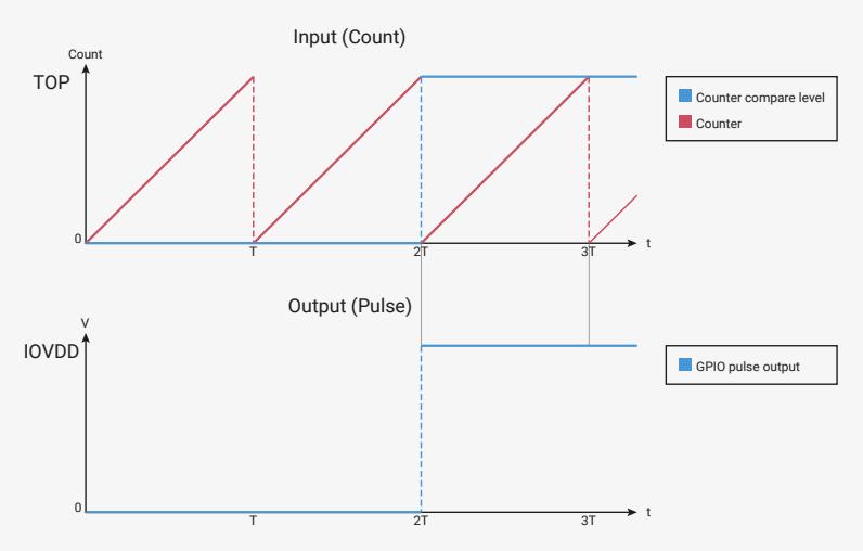
The diagram shows two vertically aligned plots sharing a common time axis \( t \) . The top plot, 'Input (Count)', has a vertical axis 'Count' with markers at 0 and \( TOP \) . A red line represents the 'Counter', which increases linearly from 0 to \( TOP \) and then resets to 0. A horizontal blue line represents the 'Counter compare level'. The bottom plot, 'Output (Pulse)', has a vertical axis 'V' with markers at 0 and \( IOVDD \) . A blue square wave represents the 'GPIO pulse output'. For \( CC = 0 \) , the output is low at 0. For \( CC = TOP + 1 \) , the output is high at \( IOVDD \) for the entire period \( T \) .
A \( CC \) value of 0 produces a 0% output: the output signal is always low. A \( CC \) value of \( TOP + 1 \) (equal to the period when not phase-corrected) produces a 100% output. If \( TOP \) is 254, the counter has a period of 255 cycles, and \( CC \) values in the range of 0 to 255 inclusive will produce duty cycles in the range 0% to 100% inclusive.
Glitch-free output at 0% and 100% helps avoid switching losses, for instance, when a MOSFET is controlled at its minimum and maximum current levels.
12.5.2.3. Double buffering
Figure 116 shows how a change in input value produces a change in output duty cycle. This can approximate analogue waveforms such as a sine wave.
Figure 116. The input value varies with each counter period: first \( TOP/3 \) , then \( 2 \times TOP/3 \) , and finally \( TOP + 1 \) for 100% duty cycle. Each increase in the input value causes a corresponding increase in the output duty cycle.
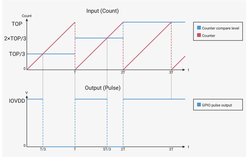
The diagram consists of two vertically aligned plots sharing a common time axis \( t \) .
- Top Plot (Input (Count)): The y-axis is labeled 'Count' with values \( 0 \) , \( TOP/3 \) , \( 2 \times TOP/3 \) , and \( TOP \) . A red line represents the 'Counter' value, which increases linearly from \( 0 \) to \( TOP \) over each period \( T \) . Blue horizontal segments represent the 'Counter compare level'. These levels are \( 0 \) for the first \( T/3 \) of each period, \( TOP/3 \) for the next \( T/3 \) , and \( 2 \times TOP/3 \) for the final \( T/3 \) . At the end of each period, the counter wraps back to \( 0 \) .
- Bottom Plot (Output (Pulse)): The y-axis is labeled 'V' with values \( 0 \) and \( IOVDD \) . A blue square wave represents the 'GPIO pulse output'. The pulse is at \( IOVDD \) for the duration of the counter compare level and at \( 0 \) otherwise. The duty cycle increases in steps as the compare level increases.
In Figure 116, the input value only changes at the instant where the counter wraps through \( 0 \) . Figure 117 shows what happens if the input value is allowed to change at any other time: an unwanted glitch is produced at the output.
Figure 117. The input value changes whilst the counter is mid-ramp. This produces additional toggling at the output.
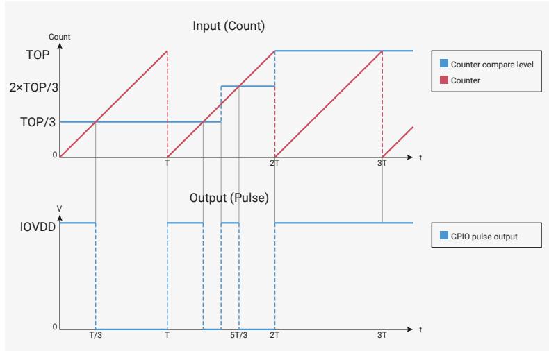
The diagram is similar to Figure 116 but includes an additional change to the input value.
- Top Plot (Input (Count)): The counter (red line) ramps up. At time \( 5T/3 \) , the counter compare level (blue step) changes from \( TOP/3 \) to \( 2 \times TOP/3 \) mid-ramp. This causes the counter to effectively jump, creating a glitch in the output.
- Bottom Plot (Output (Pulse)): The GPIO pulse output (blue square wave) shows an additional narrow pulse at \( IOVDD \) at time \( 5T/3 \) , corresponding to the mid-ramp change in the input value.
The behaviour becomes even more perplexing if the \( TOP \) register is also modified. It would be difficult for software to write to \( CC \) or \( TOP \) with the correct timing. To solve this, each slice has two copies of the \( CC \) and \( TOP \) registers: one copy that software can modify, and another, internal copy that is updated from the first register at the instant the counter wraps. Software can modify its copy of the register at will, but the changes are not captured by the PWM output until the next wrap.
Figure 118 shows the sequence of events where a software interrupt handler changes the value of \( CC_A \) each time the counter wraps.
Figure 118. Each counter wrap causes the interrupt request signal to assert. The processor enters its interrupt handler, writes to its copy of the CC register, and clears the interrupt. When the counter wraps again, the latched version of the CC register is instantaneously updated with the most recent value written by software, and this value controls the duty cycle for the next period. The IRQ is reasserted so that software can write another fresh value to its copy of the CC register.
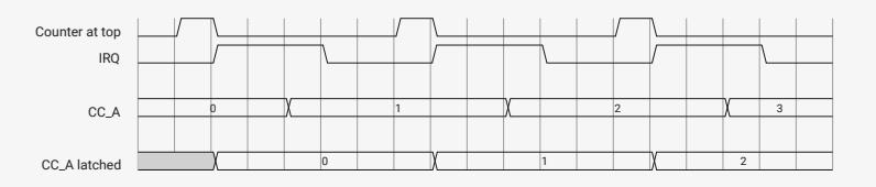
The diagram shows four digital signals over time. The top signal, 'Counter at top', is a periodic square wave. The second signal, 'IRQ', is a square wave that asserts (goes high) at each transition of the counter from high to low. The third signal, 'CC_A', is a square wave that changes value at each IRQ assertion, with values 0, 1, 2, and 3 shown. The bottom signal, 'CC_A latched', is a square wave that remains at its current value until the next IRQ assertion, at which point it updates to the new CC_A value.
There is no limitation on what values can be written to CC or TOP , or when they are written. In normal PWM mode ( CSR_PH_CORRECT is 0), the latched copies update when the counter wraps to 0, which occurs once every TOP + 1 cycles. In phase-correct mode ( CSR_PH_CORRECT is 1), the latched copies update on the 0 to 0 count transition, when the counter stops counting downward and begins to count upward again.
12.5.2.4. Clock divider
Each slice has a 8 integer bit, 4 fractional bit fractional clock divider configured by the DIV register. The clock divider allows you to slow the count rate by a factor of up to 256. To do this, the PWM generates an enable signal that gates counter operation. This allows you to achieve output frequencies significantly lower than the system clock. For instance, from a 125MHz system clock, the clock divider can slow the count rate to approximately 7.5Hz. Lower frequencies than this require a system timer interrupt (Section 12.8).
Figure 119. The clock divider generates an enable signal. The counter only counts on cycles where this signal is high. A clock divisor of 1 causes the enable to be asserted on every cycle, so the counter counts by one on every system clock cycle. Higher divisors cause the count enable to be asserted less frequently. Fractional division achieves an average fractional counting rate by spacing some enable pulses further apart than others.
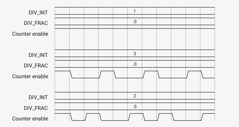
The diagram shows three sets of signals for different clock divisors. Each set includes 'DIV_INT' (integer part), 'DIV_FRAC' (fractional part), and 'Counter enable' (the resulting gate signal).
- For divisor 1: DIV_INT is 1, DIV_FRAC is .0. The counter enable signal is a continuous high line.
- For divisor 3: DIV_INT is 3, DIV_FRAC is .0. The counter enable signal is a square wave that is high for 3 full system clock cycles and then low for 1 cycle.
- For divisor 2.5: DIV_INT is 2, DIV_FRAC is .5. The counter enable signal is a square wave that is high for 2 full system clock cycles and then high for half of the next cycle.
The fractional divider is a first-order delta-sigma type. The clock divider also extends the effective count range when using level-sensitive or edge-sensitive modes to take duty cycle or frequency measurements.
12.5.2.5. Level-sensitive and edge-sensitive triggering
The PWM provides the following counter modes:
- • Default free-running, counting continuously whenever the slice is enabled (free-running)
- • Count continuously when a high level is detected on the B pin (level sensitive)
- • Count once with each rising edge detected on the B pin (rising edge-sensitive)
- • Count once with each falling edge detected on the B pin (falling edge-sensitive)
Figure 120. PWM slice event selection. The counter advances when its enable input is high. This enable is generated by two sequential stages. First, any one of four event types (always on, pin B high, pin B rise, pin B fall) can generate enable pulses for the fractional clock divider. The divider can reduce the rate of the enable pulses, before passing them on to the counter.
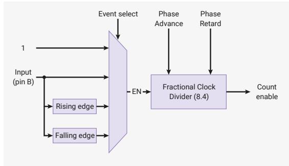
Use the
DIVMODE
field in each slice's
CSR
to select a mode. In free-running mode, the A and B pins are both outputs. In any other mode, the B pin becomes an input that controls counter operation.
CC_B
is ignored when not in free-running mode.
You can measure the duty cycle or frequency of an input signal by running the slice for a fixed amount of time in level-sensitive or edge-sensitive mode. Due to the type of edge-detect circuit used, the low period and high period of the measured signal must both be strictly greater than the system clock period when taking frequency measurements.
The clock divider still operates in level-sensitive and edge-sensitive modes. At maximum division (
DIV_INT
is 0), the counter only advances once per 256 high input cycles in level-sensitive modes, or once per 256 edges in edge-sensitive mode. This allows you to take longer-running measurements, although the resolution is still 16 bits.
Pico Examples: https://github.com/raspberrypi/pico-examples/blob/master/pwm/measure_duty_cycle/measure_duty_cycle.c Lines 19 - 37
19 float measure_duty_cycle(uint gpio) {
20     // Only the PWM B pins can be used as inputs.
21     assert(pwm_gpio_to_channel(gpio) == PWM_CHAN_B);
22     uint slice_num = pwm_gpio_to_slice_num(gpio);
23
24     // Count once for every 100 cycles the PWM B input is high
25     pwm_config cfg = pwm_get_default_config();
26     pwm_config_set_clkdiv_mode(&cfg, PWM_DIV_B_HIGH);
27     pwm_config_set_clkdiv(&cfg, 100);
28     pwm_init(slice_num, &cfg, false);
29     gpio_set_function(gpio, GPIO_FUNC_PWM);
30
31     pwm_set_enabled(slice_num, true);
32     sleep_ms(10);
33     pwm_set_enabled(slice_num, false);
34     float counting_rate = clock_get_hz(clk_sys) / 100;
35     float max_possible_count = counting_rate * 0.01;
36     return pwm_get_counter(slice_num) / max_possible_count;
37 }
12.5.2.6. Configuring PWM period
When free-running, use the following three parameters to control the period of a PWM slice's output (measured in system clock cycles):
- • The
TOPregister, which controls the maximum value of the counting period - • The
CSR_PH_CORRECTbit, which enables phase-correct mode - • The
DIVregister, which controls the clock divider
The slice counts from 0 to
TOP
, then either wraps or begins counting backward, depending on the setting of
CSR_PH_CORRECT
. The clock divider slows the rate of counting, with a maximum speed of one count per cycle, and a minimum speed of one count per 256 cycles. Calculate the period in clock cycles with the following equation:
33     }
34 }
35 // Square the fade value to make the LED's brightness appear more linear
36 // Note this range matches with the wrap value
37 pwm_set_gpio_level(PICO_DEFAULT_LED_PIN, fade * fade);
38 }
39
40 int main() {
41 #ifndef PICO_DEFAULT_LED_PIN
42 #warning pwm/led_fade example requires a board with a regular LED
43 #else
44     // Tell the LED pin that the PWM is in charge of its value.
45     gpio_set_function(PICO_DEFAULT_LED_PIN, GPIO_FUNC_PWM);
46     // Figure out which slice we just connected to the LED pin
47     uint slice_num = pwm_gpio_to_slice_num(PICO_DEFAULT_LED_PIN);
48
49     // Mask our slice's IRQ output into the PWM block's single interrupt line,
50     // and register our interrupt handler
51     pwm_clear_irq(slice_num);
52     pwm_set_irq_enabled(slice_num, true);
53     irq_set_exclusive_handler(PWM_DEFAULT_IRQ_NUM(), on_pwm_wrap);
54     irq_set_enabled(PWM_DEFAULT_IRQ_NUM(), true);
55
56     // Get some sensible defaults for the slice configuration. By default, the
57     // counter is allowed to wrap over its maximum range (0 to 2**16-1)
58     pwm_config config = pwm_get_default_config();
59     // Set divider, reduces counter clock to sysclock/this value
60     pwm_config_set_clkdiv(&config, 4.f);
61     // Load the configuration into our PWM slice, and set it running.
62     pwm_init(slice_num, &config, true);
63
64     // Everything after this point happens in the PWM interrupt handler, so we
65     // can twiddle our thumbs
66     while (1)
67         tight_loop_contents();
68 #endif
69 }
This scheme allows multiple slices to generate interrupts concurrently. A system interrupt handler determines which slices caused the most recent interruption, and handles them appropriately. Normally, this means reloading those slices' TOP or CC registers, but the PWM block can also be used as a source of regular interrupt requests for non-PWM purposes.
The same pulse which sets the interrupt flag in INTR is also available as a one-cycle data request to the RP2350 system DMA. For each cycle the DMA sees a DREQ asserted, it makes one data transfer to its programmed location in as timely a manner as possible. Combined with the double-buffered behaviour of CC and TOP , the DMA can efficiently stream data to a PWM slice at a rate of one transfer per counter period. Alternatively, a PWM slice could serve as a pacing timer for DMA transfers to some other memory-mapped hardware.
12.5.2.8. On-the-fly phase adjustment
For some applications, it is necessary to control the phase relationship between two PWM outputs on different slices.
The global enable register EN contains an alias of the CSR_EN flag for each slice. Use this register to start and stop several slices simultaneously. If two slices with the same output frequency start at the same time, they run in perfect lockstep, with a fixed phase relationship determined by the initial counter values.
The CSR_PH_ADV and CSR_PH_RET fields advance or retard a slice's output phase by one count whilst it is running. They do so by inserting or deleting pulses from the clock enable (the output of the clock divider), as shown in Figure 121 .
Figure 121. The clock enable signal, output by the clock divider, controls the rate of counting. Phase advance forces the clock enable high on cycles where it is low, causing the counter to jump forward by one count. Phase retard forces the clock enable low when it would be high, holding the counter back by one count.
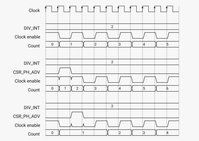
The figure shows three timing scenarios for a counter. In all scenarios, a 'Clock' signal is provided as a series of pulses. The 'DIV_INT' signal is a constant high level with a '2' indicating a division factor. The 'Clock enable' signal is derived from the clock and DIV_INT. The 'Count' signal shows the counter's state over time.
- Scenario 1 (Top): The 'Clock enable' signal is high during clock pulses. The 'Count' signal increments from 0 to 5.
- Scenario 2 (Middle): The 'CSR_PH_ADV' signal is high during a clock pulse. The 'Clock enable' signal is high during that pulse, causing the counter to skip a count. The 'Count' signal increments from 0 to 6.
- Scenario 3 (Bottom): The 'CSR_PH_ADV' signal is low during a clock pulse. The 'Clock enable' signal is low during that pulse, causing the counter to skip a count. The 'Count' signal increments from 0 to 4.
The counter cannot count faster than once per cycle, so PH_ADV requires DIV_INT > 1 or DIV_FRAC > 0. Likewise, the counter will not start to count backward if PH_RET is asserted when the clock enable is permanently low.
To advance or retard the phase by one count, software writes 1 to PH_ADV or PH_RET . Once an enable pulse has been inserted or deleted, the PH_ADV or PH_RET register bit returns to 0. Software can poll CSR until this happens. PH_ADV always inserts a pulse into the next available gap; PH_RET always deletes the next available pulse.
12.5.3. List of registers
The PWM registers start at a base address of 0x400a8000 (defined as PWM_BASE in the SDK).
Table 1131. List of PWM registers
| Offset 0x42fc8 0x42fcc 0x42fd0 0x42fd4 0x42fd8 | Name DEVID DEVTYPE PIDR4 PIDR5 PIDR6 | Info Device Configuration register Device Type Identifier register CoreSight Periperal ID4 CoreSight Periperal ID5 CoreSight Periperal ID6 |
|---|---|---|
| cycles where it is low, causing the counter to jump forward by one | Count 0 1 | 2 3 4 5 |
| count. Phase retard forces the clock enable low when it | DIV_INT CSR_PH_ADV | 2 |
| would be high, holding the counter back by one count. | Clock enable Count 0 1 2 | 3 4 5 6 |
| Clock enable Count 0 | 1 2 3 4 | |
| The counter cannot count faster than once per cycle, so | PH_ADV requires DIV_INT > 1 or DIV_FRAC > 0. Likewise, the counter | |
| will not start to count backward if | PH_RET | is asserted when the clock enable is permanently low. |
| To advance or retard the phase by one count, software writes 1 to | PH_ADV or PH_RET . Once an enable pulse has been | |
| inserted or deleted, the | PH_ADV or PH_RET | register bit returns to 0. Software can poll CSR until this happens. PH_ADV always |
| inserts a pulse into the next available gap; | PH_RET always deletes the next available pulse. | |
| The PWM registers start at a base address of Table 1131. List of | 0x400a8000 (defined as PWM_BASE in the SDK). | |
| Offset PWM registers | Name | Info |
| 0x000 | CH0_CSR | Control and status register |
| 0x004 | CH0_DIV | INT and FRAC form a fixed-point fractional number. Counting rate is system clock frequency divided by this number. |
| 0x008 | CH0_CTR | Fractional division uses simple 1st-order sigma-delta. Direct access to the PWM counter |
| 0x00c | CH0_CC | Counter compare values |
| 0x010 | CH0_TOP | Counter wrap value |
| 0x014 | CH1_CSR | Control and status register |
| 0x018 | CH1_DIV | INT and FRAC form a fixed-point fractional number. Counting rate is system clock frequency divided by this number. |
| 0x01c | CH1_CTR | Fractional division uses simple 1st-order sigma-delta. Direct access to the PWM counter |
| 0x020 | CH1_CC | Counter compare values |
| 0x024 | CH1_TOP | Counter wrap value |
| 0x028 | CH2_CSR | Control and status register |
| 0x02c | CH2_DIV | INT and FRAC form a fixed-point fractional number. Counting rate is system clock frequency divided by this number. |
| Offset | Name | Info |
|---|---|---|
| 0x0a4 | CH8_DIV | INT and FRAC form a fixed-point fractional number. Counting rate is system clock frequency divided by this number. Fractional division uses simple 1st-order sigma-delta. |
| 0x0a8 | CH8_CTR | Direct access to the PWM counter |
| 0x0ac | CH8_CC | Counter compare values |
| 0x0b0 | CH8_TOP | Counter wrap value |
| 0x0b4 | CH9_CSR | Control and status register |
| 0x0b8 | CH9_DIV | INT and FRAC form a fixed-point fractional number. Counting rate is system clock frequency divided by this number. Fractional division uses simple 1st-order sigma-delta. |
| 0x0bc | CH9_CTR | Direct access to the PWM counter |
| 0x0c0 | CH9_CC | Counter compare values |
| 0x0c4 | CH9_TOP | Counter wrap value |
| 0x0c8 | CH10_CSR | Control and status register |
| 0x0cc | CH10_DIV | INT and FRAC form a fixed-point fractional number. Counting rate is system clock frequency divided by this number. Fractional division uses simple 1st-order sigma-delta. |
| 0x0d0 | CH10_CTR | Direct access to the PWM counter |
| 0x0d4 | CH10_CC | Counter compare values |
| 0x0d8 | CH10_TOP | Counter wrap value |
| 0x0dc | CH11_CSR | Control and status register |
| 0x0e0 | CH11_DIV | INT and FRAC form a fixed-point fractional number. Counting rate is system clock frequency divided by this number. Fractional division uses simple 1st-order sigma-delta. |
| 0x0e4 | CH11_CTR | Direct access to the PWM counter |
| 0x0e8 | CH11_CC | Counter compare values |
| 0x0ec | CH11_TOP | Counter wrap value |
| 0x0f0 | EN | This register aliases the CSR_EN bits for all channels. Writing to this register allows multiple channels to be enabled or disabled simultaneously, so they can run in perfect sync. For each channel, there is only one physical EN register bit, which can be accessed through here or CHx_CSR. |
| 0x0f4 | INTR | Raw Interrupts |
| 0x0f8 | IRQ0_INTE | Interrupt Enable for irq0 |
| 0x0fc | IRQ0_INTF | Interrupt Force for irq0 |
| 0x100 | IRQ0_INTS | Interrupt status after masking & forcing for irq0 |
| 0x104 | IRQ1_INTE | Interrupt Enable for irq1 |
| 0x108 | IRQ1_INTF | Interrupt Force for irq1 |
| 0x10c | IRQ1_INTS | Interrupt status after masking & forcing for irq1 |
PWM: CH0_CSR, CH1_CSR, ..., CH10_CSR, CH11_CSR Registers
Offsets: 0x000, 0x014, ..., 0x0c8, 0x0dc
Description
Control and status register
Table 1132. CH0_CSR, CH1_CSR, ..., CH10_CSR, CH11_CSR Registers
| Bits | Description | Type | Reset |
|---|---|---|---|
| 31:8 | Reserved. | - | - |
| 7 | PH_ADV : Advance the phase of the counter by 1 count, while it is running. Self-clearing. Write a 1, and poll until low. Counter must be running at less than full speed ( \( \text{div\_int} + \text{div\_frac} / 16 > 1 \) ) | SC | 0x0 |
| 6 | PH_RET : Retard the phase of the counter by 1 count, while it is running. Self-clearing. Write a 1, and poll until low. Counter must be running. | SC | 0x0 |
| 5:4 | DIVMODE | RW | 0x0 |
| Enumerated values: | |||
| 0x0 → DIV: Free-running counting at rate dictated by fractional divider | |||
| 0x1 → LEVEL: Fractional divider operation is gated by the PWM B pin. | |||
| 0x2 → RISE: Counter advances with each rising edge of the PWM B pin. | |||
| 0x3 → FALL: Counter advances with each falling edge of the PWM B pin. | |||
| 3 | B_INV : Invert output B | RW | 0x0 |
| 2 | A_INV : Invert output A | RW | 0x0 |
| 1 | PH_CORRECT : 1: Enable phase-correct modulation. 0: Trailing-edge | RW | 0x0 |
| 0 | EN : Enable the PWM channel. | RW | 0x0 |
PWM: CH0_DIV, CH1_DIV, ..., CH10_DIV, CH11_DIV Registers
Offsets: 0x004, 0x018, ..., 0x0cc, 0x0e0
Description
INT and FRAC form a fixed-point fractional number.
Counting rate is system clock frequency divided by this number.
Fractional division uses simple 1st-order sigma-delta.
Table 1133. CH0_DIV, CH1_DIV, ..., CH10_DIV, CH11_DIV Registers
| Bits | Description | Type | Reset |
|---|---|---|---|
| 31:12 | Reserved. | - | - |
| 11:4 | INT | RW | 0x01 |
| 3:0 | FRAC | RW | 0x0 |
PWM: CH0_CTR, CH1_CTR, ..., CH10_CTR, CH11_CTR Registers
Offsets: 0x008, 0x01c, ..., 0x0d0, 0x0e4
Table 1134. CH0_CTR, CH1_CTR, ..., CH10_CTR, CH11_CTR Registers
| Bits | Description | Type | Reset |
|---|---|---|---|
| 31:16 | Reserved. | - | - |
| 15:0 | Direct access to the PWM counter | RW | 0x0000 |
PWM: CH0_CC, CH1_CC, ..., CH10_CC, CH11_CC Registers
Offsets: 0x00c, 0x020, ..., 0x0d4, 0x0e8
Description
Counter compare values
Table 1135. CH0_CC, CH1_CC, ..., CH10_CC, CH11_CC Registers
| Bits | Description | Type | Reset |
|---|---|---|---|
| 31:16 | B | RW | 0x0000 |
| 15:0 | A | RW | 0x0000 |
PWM: CH0_TOP, CH1_TOP, ..., CH10_TOP, CH11_TOP Registers
Offsets: 0x010, 0x024, ..., 0x0d8, 0x0ec
Table 1136. CH0_TOP, CH1_TOP, ..., CH10_TOP, CH11_TOP Registers
| Bits | Description | Type | Reset |
|---|---|---|---|
| 31:16 | Reserved. | - | - |
| 15:0 | Counter wrap value | RW | 0xffff |
PWM: EN Register
Offset: 0x0f0
Description
This register aliases the CSR_EN bits for all channels.
Writing to this register allows multiple channels to be enabled or disabled simultaneously, so they can run in perfect sync.
For each channel, there is only one physical EN register bit, which can be accessed through here or CHx_CSR.
Table 1137. EN Register
| Bits | Description | Type | Reset |
|---|---|---|---|
| 31:12 | Reserved. | - | - |
| 11 | CH11 | RW | 0x0 |
| 10 | CH10 | RW | 0x0 |
| 9 | CH9 | RW | 0x0 |
| 8 | CH8 | RW | 0x0 |
| 7 | CH7 | RW | 0x0 |
| 6 | CH6 | RW | 0x0 |
| 5 | CH5 | RW | 0x0 |
| 4 | CH4 | RW | 0x0 |
| 3 | CH3 | RW | 0x0 |
| 2 | CH2 | RW | 0x0 |
| 1 | CH1 | RW | 0x0 |
| Bits | Description | Type | Reset |
|---|---|---|---|
| 0 | CH0 | RW | 0x0 |
PWM: INTR Register
Offset: 0x0f4
Description
Raw Interrupts
Table 1138. INTR Register
| Bits | Description | Type | Reset |
|---|---|---|---|
| 31:12 | Reserved. | - | - |
| 11 | CH11 | WC | 0x0 |
| 10 | CH10 | WC | 0x0 |
| 9 | CH9 | WC | 0x0 |
| 8 | CH8 | WC | 0x0 |
| 7 | CH7 | WC | 0x0 |
| 6 | CH6 | WC | 0x0 |
| 5 | CH5 | WC | 0x0 |
| 4 | CH4 | WC | 0x0 |
| 3 | CH3 | WC | 0x0 |
| 2 | CH2 | WC | 0x0 |
| 1 | CH1 | WC | 0x0 |
| 0 | CH0 | WC | 0x0 |
PWM: IRQ0_INTE Register
Offset: 0x0f8
Description
Interrupt Enable for irq0
Table 1139. IRQ0_INTE Register
| Bits | Description | Type | Reset |
|---|---|---|---|
| 31:12 | Reserved. | - | - |
| 11 | CH11 | RW | 0x0 |
| 10 | CH10 | RW | 0x0 |
| 9 | CH9 | RW | 0x0 |
| 8 | CH8 | RW | 0x0 |
| 7 | CH7 | RW | 0x0 |
| 6 | CH6 | RW | 0x0 |
| 5 | CH5 | RW | 0x0 |
| 4 | CH4 | RW | 0x0 |
| 3 | CH3 | RW | 0x0 |
| 2 | CH2 | RW | 0x0 |
| Bits | Description | Type | Reset |
|---|---|---|---|
| 1 | CH1 | RW | 0x0 |
| 0 | CH0 | RW | 0x0 |
PWM: IRQ0_INTF Register
Offset: 0x0fc
Description
Interrupt Force for irq0
Table 1140.
IRQ0_INTF Register
| Bits | Description | Type | Reset |
|---|---|---|---|
| 31:12 | Reserved. | - | - |
| 11 | CH11 | RW | 0x0 |
| 10 | CH10 | RW | 0x0 |
| 9 | CH9 | RW | 0x0 |
| 8 | CH8 | RW | 0x0 |
| 7 | CH7 | RW | 0x0 |
| 6 | CH6 | RW | 0x0 |
| 5 | CH5 | RW | 0x0 |
| 4 | CH4 | RW | 0x0 |
| 3 | CH3 | RW | 0x0 |
| 2 | CH2 | RW | 0x0 |
| 1 | CH1 | RW | 0x0 |
| 0 | CH0 | RW | 0x0 |
PWM: IRQ0_INTS Register
Offset: 0x100
Description
Interrupt status after masking & forcing for irq0
Table 1141.
IRQ0_INTS Register
| Bits | Description | Type | Reset |
|---|---|---|---|
| 31:12 | Reserved. | - | - |
| 11 | CH11 | RO | 0x0 |
| 10 | CH10 | RO | 0x0 |
| 9 | CH9 | RO | 0x0 |
| 8 | CH8 | RO | 0x0 |
| 7 | CH7 | RO | 0x0 |
| 6 | CH6 | RO | 0x0 |
| 5 | CH5 | RO | 0x0 |
| 4 | CH4 | RO | 0x0 |
| 3 | CH3 | RO | 0x0 |
| Bits | Description | Type | Reset |
|---|---|---|---|
| 2 | CH2 | RO | 0x0 |
| 1 | CH1 | RO | 0x0 |
| 0 | CH0 | RO | 0x0 |
PWM: IRQ1_INTE Register
Offset: 0x104
Description
Interrupt Enable for irq1
Table 1142.
IRQ1_INTE Register
| Bits | Description | Type | Reset |
|---|---|---|---|
| 31:12 | Reserved. | - | - |
| 11 | CH11 | RW | 0x0 |
| 10 | CH10 | RW | 0x0 |
| 9 | CH9 | RW | 0x0 |
| 8 | CH8 | RW | 0x0 |
| 7 | CH7 | RW | 0x0 |
| 6 | CH6 | RW | 0x0 |
| 5 | CH5 | RW | 0x0 |
| 4 | CH4 | RW | 0x0 |
| 3 | CH3 | RW | 0x0 |
| 2 | CH2 | RW | 0x0 |
| 1 | CH1 | RW | 0x0 |
| 0 | CH0 | RW | 0x0 |
PWM: IRQ1_INTF Register
Offset: 0x108
Description
Interrupt Force for irq1
Table 1143.
IRQ1_INTF Register
| Bits | Description | Type | Reset |
|---|---|---|---|
| 31:12 | Reserved. | - | - |
| 11 | CH11 | RW | 0x0 |
| 10 | CH10 | RW | 0x0 |
| 9 | CH9 | RW | 0x0 |
| 8 | CH8 | RW | 0x0 |
| 7 | CH7 | RW | 0x0 |
| 6 | CH6 | RW | 0x0 |
| 5 | CH5 | RW | 0x0 |
| 4 | CH4 | RW | 0x0 |
| Bits | Description | Type | Reset |
|---|---|---|---|
| 3 | CH3 | RW | 0x0 |
| 2 | CH2 | RW | 0x0 |
| 1 | CH1 | RW | 0x0 |
| 0 | CH0 | RW | 0x0 |
PWM: IRQ1_INTS Register
Offset: 0x10c
Description
Interrupt status after masking & forcing for irq1
Table 1144.
IRQ1_INTS Register
| Bits | Description | Type | Reset |
|---|---|---|---|
| 31:12 | Reserved. | - | - |
| 11 | CH11 | RO | 0x0 |
| 10 | CH10 | RO | 0x0 |
| 9 | CH9 | RO | 0x0 |
| 8 | CH8 | RO | 0x0 |
| 7 | CH7 | RO | 0x0 |
| 6 | CH6 | RO | 0x0 |
| 5 | CH5 | RO | 0x0 |
| 4 | CH4 | RO | 0x0 |
| 3 | CH3 | RO | 0x0 |
| 2 | CH2 | RO | 0x0 |
| 1 | CH1 | RO | 0x0 |
| 0 | CH0 | RO | 0x0 |
12.6. DMA
The RP2350 Direct Memory Access (DMA) controller performs bulk data transfers on a processor’s behalf. This leaves processors free to attend to other tasks or enter low-power sleep states. The DMA dual bus manager ports can issue one read and one write access per cycle. The data throughput is therefore far greater than one of RP2350’s processors.
Figure 122. DMA Architecture Overview. The read manager can read data from some address every clock cycle. Likewise, the write manager can write to another address. The address generator produces matched pairs of read and write addresses, which the managers consume through the address FIFOs. The DMA can run up to 16 transfer sequences simultaneously, supervised by software via the control and status registers.
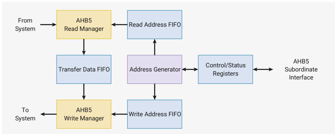
The DMA can perform one read access and one write access, up to 32 bits in size, every clock cycle. There are 16 independent channels, each of which supervises a sequence of bus transfers in one of the following scenarios:
Memory-to-peripheral
a peripheral signals the DMA when it needs more data to transmit. The DMA reads data from an array in RAM or flash, and writes to the peripheral's data FIFO.
Peripheral-to-memory
a peripheral signals the DMA when it has received data. The DMA reads this data from the peripheral's data FIFO, and writes it to an array in RAM.
Memory-to-memory
the DMA transfers data between two buffers in RAM, as fast as possible.
Each channel has its own control and status registers (CSRs) that software can use to program and monitor the channel's progress. When multiple channels are active at the same time, the DMA shares bandwidth evenly between the channels, with round-robin over all channels that are currently requesting data transfers.
The transfer size can be either 32, 16, or 8 bits. This is configured once for each channel: source transfer size and destination transfer size are the same. The DMA performs byte lane replication on narrow writes, so byte data is available in all 4 bytes of the databus, and halfword data in both halfwords.
Channels can be combined in varied ways for more sophisticated behaviour and greater autonomy. For example, one channel can configure another, loading configuration data from a sequence of control blocks in memory, and the second can then call back to the first via the
CHAIN_TO
option when it needs to be reconfigured.
Making the DMA more autonomous means that much less processor supervision is required: overall this allows the system to do more at once, or to dissipate less power.
12.6.1. Changes from RP2040
The following new features have been added:
- • Increased the number of DMA channels from 12 to 16.
- • Increased the number of shared IRQ outputs from 2 to 4.
- • Channels can be assigned to security domains using
SECCFG_CH0throughSECCFG_CH15. - • The DMA now filters bus accesses using the built-in memory protection unit (Section 12.6.6.3).
- • Interrupts can be assigned to security domains using
SECCFG_IRQ0throughSECCFG_IRQ3. - • Pacing timers and the CRC sniffer can be assigned to security domains using the
SECCFG_MISCregister. - • The four most-significant bits of
TRANS_COUNT(CH0_TRANS_COUNT) are redefined as theMODEfield, which defines what happens whenTRANS_COUNTreaches zero:
- ◦ This backward-incompatible change reduces the maximum transfers in one sequence from \( 2^{32}-1 \) to \( 2^{28}-1 \) .
- ◦ Mode
0x0has the same behaviour as RP2040, so there is no need to modify software that performs less than 256 million transfers at a time. - ◦ Mode
0x1, "trigger self", allows a channel to automatically restart itself after finishing a transfer sequence, in addition to the usual end-of-sequence actions like raising an interrupt or triggering other channels. This can be used for example to get periodic interrupts from streaming ring buffer transfers. - ◦ Mode
0xf, "endless", allows a channel to run forever:TRANS_COUNTdoes not decrement. - • New
CH0_CTRL_TRIG.INCR_READ_REVandCH0_CTRL_TRIG.INCR_WRITE_REVfields allow addresses to decrement rather than increment, or to increment by two.- ◦ Some existing fields in the
CTRLregisters, such asCH0_CTRL_TRIG.BUSY, have moved to accommodate the new fields.
- ◦ Some existing fields in the
Some existing behaviour has been refined:
- • The logic that adjusts values read from
WRITE_ADDRandREAD_ADDRaccording to the number of in-flight transfers is disabled for address-wrapping and non-incrementing transfers (erratum RP2040-E12). - • You can now poll the
ABORTregister to wait for completion of an aborted channel (erratum RP2040-E13). - • DMA completion actions such as
CHAIN_TOare now strictly ordered against the last write completion, so aCHAIN_TOon a channel whose registers you write to is a well-defined operation.- ◦ This enables the use of control blocks that don't include one of the four trigger register aliases.
- ◦ Previously, a channel was considered to complete on the first cycle of its last write's data phase. Now, a channel is considered to complete on the last cycle of its last write's data phase. This is usually the same cycle, but it can be later when the DMA encounters a write data-phase bus stall.
- • Previously, the DMA's internal arbitration logic inserted an idle cycle after completing a round of active high-priority channels (
CH0_CTRL_TRIG.HIGH_PRIORITY), even if there were no active low-priority requests. This reduced DMA throughput when lightly loaded. This idle cycle has been removed, eliminating lost throughput. - • IRQ assertion latency has been reduced by one cycle.
12.6.2. Configuring channels
Each channel has four control/status registers:
- •
READ_ADDR(CH0_READ_ADDR) is the address of the next memory location to read. - •
WRITE_ADDR(CH0_WRITE_ADDR) is the address of the next memory location to write. - •
TRANS_COUNT(CH0_TRANS_COUNT) shows the number of transfers remaining in the current transfer sequence and programs the number of transfers in the next transfer sequence (see Section 12.6.2.2 ). - •
CTRL(CH0_CTRL_TRIG) configures all other aspects of the channel's behaviour, enables/disables the channel, and provides completion status.
To directly instruct the DMA channel to perform a data transfer, software writes to these four registers, and then triggers the channel ( Section 12.6.3 ). To make the DMA more autonomous, you can also program one DMA channel to write to another channel's configuration registers, queueing up many transfer sequences in advance.
All four are live registers; they update their status continuously as the channel progresses.
12.6.2.1. Read and write addresses
READ_ADDR
and
WRITE_ADDR
contain the address the channel will next read from, and write to, respectively. These registers update automatically after each read/write access, incrementing to the next read/write address as required. The size of the increment varies according to:
- • the transfer size: 1, 2 or 4 byte bus accesses as per
CH0_CTRL_TRIG.DATA_SIZE - • the increment enable for each address register:
CH0_CTRL_TRIG.INCR_READandCH0_CTRL_TRIG.INCR_WRITE - • the increment direction:
CH0_CTRL_TRIG.INCR_READ_REVandCH0_CTRL_TRIG.INCR_WRITE_REV
Software should generally program these registers with new start addresses each time a new transfer sequence starts. If
READ_ADDR
and
WRITE_ADDR
are not reprogrammed, the DMA will use the current values as start addresses for the next transfer. For example:
- • If the address does not increment (e.g. it is the address of a peripheral FIFO), and the next transfer sequence is to/from that same address, there is no need to write to the register again.
- • When transferring to/from a consecutive series of buffers in memory (e.g. scattering and gathering), an address register will already have incremented to the start of the next buffer at the completion of a transfer.
By not programming all four CSRs for each transfer sequence, software can use shorter interrupt handlers, and more compact control block formats when used with channel chaining (see register aliases in Section 12.6.3.1 , chaining in Section 12.6.3.2 ).
12.6.2.1.1. Address alignment
READ_ADDR
and
WRITE_ADDR
must be aligned to the transfer size, specified in
CH0_CTRL_TRIG.DATA_SIZE
. For 32-bit transfers, the address must be a multiple of four, and for 16-bit transfers, the address must be a multiple of two. Software is responsible for correctly aligning addresses written to
READ_ADDR
and
WRITE_ADDR
: the DMA does not enforce alignment.
If software initially writes a correctly aligned address, the address will remain correctly aligned throughout the transfer sequence, because the DMA always increments
READ_ADDR
and
WRITE_ADDR
by a multiple of the transfer size. Specifically, it increments by transfer size times -1, 0, 1 or 2, depending on the values of
CH0_CTRL_TRIG.INCR_READ
,
CH0_CTRL_TRIG.INCR_WRITE
,
CH0_CTRL_TRIG.INCR_READ_REV
and
CH0_CTRL_TRIG.INCR_WRITE_REV
.
The DMA MPU and system-level bus security filters perform protection checks on the lowest byte address of all bytes transferred on a given cycle (i.e. to the present value of
READ_ADDR/WRITE_ADDR
). RP2350 memory hardware ensures unaligned bus accesses do not cause data to be read/written from the other side of a protection boundary. This means that unaligned access can not be used to violate the memory protection model. Other than this, the result of an unaligned access is unspecified.
12.6.2.2. Transfer count
Reading
TRANS_COUNT
(
CH0_TRANS_COUNT
) returns the number of transfers remaining in the current transfer sequence. This value updates continuously as the channel progresses. Writing to
TRANS_COUNT
sets the length of the
next
transfer sequence. Up to
\(
2^{28}-1
\)
transfers can be performed in one sequence (
0xffffffff
, approximately 256 million).
Each time the channel starts a new transfer sequence, the most recent value written to
TRANS_COUNT
is copied to the live transfer counter, which will then start to decrement again as the new transfer sequence makes progress. For debugging purposes, the
DBG_TCR
(
TRANS_COUNT
reload value) registers display the last value written to each channel's
TRANS_COUNT
.
If the channel is triggered multiple times without intervening writes to
TRANS_COUNT
, it performs the same number of transfers each time. For example, when chained to, one channel might load a fixed-size control block into another channel's CSRs.
TRANS_COUNT
would be programmed once by software, and then reload automatically every time.
Alternatively,
TRANS_COUNT
can be written with a new value before starting each transfer sequence. If
TRANS_COUNT
is the channel trigger (see
Section 12.6.3.1
), the channel will start immediately, and the value just written will be used,
not
the value currently in the reload register.
The
TRANS_COUNT
is the number of
transfers
to be performed. The total number of bytes transferred is
TRANS_COUNT
times the size of each transfer in bytes, given by
CTRL.DATA_SIZE
.
The four most-significant bits of
TRANS_COUNT
contain the
MODE
field (
CHO_TRANS_COUNT.MODE
), which modifies the counting behaviour of
TRANS_COUNT
. Mode
0x0
is the default:
TRANS_COUNT
decrements once for every bus transfer, and the channel halts once
TRANS_COUNT
reaches zero and all in-flight transfers have finished. The value of
0x0
is chosen for backward-compatibility with RP2040 software, which expects the
TRANS_COUNT
register to contain a 32-bit count rather than a 4-bit mode and a 28-bit count. There are few use cases for a
finite
number of transfers greater than
\(
2^{28}
\)
, which is why the four most-significant bits have been reallocated for use with endless transfers.
Mode
0x1
,
TRIGGER_SELF
, behaves the same as mode
0x0
, except that rather than halting upon completion, the channel immediately re-triggers itself. This is equivalent to a trigger performed by any other mechanism (Section 12.6.3):
TRANS_COUNT
is reloaded, and the channel resumes from the current
READ_ADDR
and
WRITE_ADDR
addresses. A completion interrupt is still raised (if
CTRL.IRQ_QUIET
is not set) and the specified
CHAIN_TO
operation is still performed. The main use for this mode is streaming through SRAM ring buffers, where some action is required at regular intervals, for example requesting the processor to refill an audio buffer once it is half-empty.
Mode
0xf
,
ENDLESS
, disables the decrement of
TRANS_COUNT
. This means a channel will generally run indefinitely without pause, though triggering a channel with a mode of
0xf
and a count of
0x0
will result in the channel halting immediately.
All other values are reserved for future use and their effect is unspecified.
12.6.2.3. Control/StatusThe
CTRL
register (
CHO_CTRL_TRIG
) has more, smaller fields than the other 3 registers. Among other things,
CTRL
is used to:
- • Configure the size of this channel's data transfers through the
DATA_SIZEfield. Reads are always the same size as writes. - • Configure if and how
READ_ADDRandWRITE_ADDRincrement after each read or write through theINCR_READ,INCR_READ_REV,INCR_WRITE,INCR_WRITE_REV,RING_SEL, andRING_SIZEfields. Ring transfers are available, where one of the address pointers wraps at some power-of-2 boundary. - • Select another channel (or none) to trigger when this channel completes through the
CHAIN_TOfield. - • Select a peripheral data request (DREQ) signal to pace this channel's transfers, via the
TREQ_SELfield. - • See when the channel is idle, using the
BUSYflag. - • See if the channel has encountered a bus error in the
READ_ERRORandWRITE_ERRORflags, or the combined error status in theAHB_ERRORflag.
After a channel has been correctly configured, you must trigger it. This instructs the channel to begin scheduling bus accesses, either paced by a peripheral data request signal (DREQ) or as fast as possible. The following events can trigger a channel:
- • A write to a channel trigger register.
- • Completion of another channel whose
CHAIN_TOpoints to this channel. - • A write to the
MULTI_CHAN_TRIGGERregister (can trigger multiple channels at once).
Each trigger mechanism covers different use cases. For example, trigger registers are simple and efficient when
configuring and starting a channel in an interrupt service routine because the channel is triggered by the last configuration write.
CHAIN_TO
allows one channel to callback to another channel, which can then reconfigure the first channel.
MULTI_CHAN_TRIGGER
allows software to simply start a channel without touching any of its configuration registers.
When triggered, the channel sets its
CTRL.BUSY
flag to indicate it is actively scheduling transfers. This remains set until the transfer count reaches zero, or the channel is aborted via the
CHAN_ABORT
register (Section 12.6.8.3).
When a channel is already running, indicated by
BUSY = 1
, it ignores additional triggers. A channel that is disabled (
CTRL.EN
is clear) also ignores triggers.
12.6.3.1. Aliases and triggers
Table 1145. Control register aliases. Each channel has four control/status registers. Each register can be accessed at multiple different addresses. In each naturally-aligned group of four, all four registers appear, in different orders.
| Offset | +0x0 | +0x4 | +0x8 | +0xc (Trigger) |
|---|---|---|---|---|
| 0x00 (Alias 0) | READ_ADDR | WRITE_ADDR | TRANS_COUNT | CTRL_TRIG |
| 0x10 (Alias 1) | CTRL | READ_ADDR | WRITE_ADDR | TRANS_COUNT_TRIG |
| 0x20 (Alias 2) | CTRL | TRANS_COUNT | READ_ADDR | WRITE_ADDR_TRIG |
| 0x30 (Alias 3) | CTRL | WRITE_ADDR | TRANS_COUNT | READ_ADDR_TRIG |
The four CSRs are aliased multiple times in memory. Each of the four aliases exposes the same four physical registers, but in a different order. The final register in each alias (at offset +0xc, highlighted) is a trigger register. Writing to the trigger register starts the channel.
Often, only alias 0 is used, and aliases 1 through 3 can be ignored. To configure and start the channel, write
READ_ADDR
,
WRITE_ADDR
,
TRANS_COUNT
, and finally
CTRL
. Since
CTRL
is the trigger register in alias 0, this starts the channel.
The other aliases allow more compact control block lists when using one channel to configure another, and more efficient reconfiguration and launch in interrupt handlers:
- • Each CSR is a trigger register in one of the aliases:
- ◦ When gathering fixed-size buffers into a peripheral, the DMA channel can be configured and launched by writing only
READ_ADDR_TRIG. - ◦ When scattering from a peripheral to fixed-size buffers, the channel can be configured and launched by writing only
WRITE_ADDR_TRIG.
- ◦ When gathering fixed-size buffers into a peripheral, the DMA channel can be configured and launched by writing only
- • Useful combinations of registers appear as naturally-aligned tuples which contain a trigger register. In conjunction with channel chaining and address wrapping, these implement compressed control block formats, e.g.:
- ◦ (
WRITE_ADDR,TRANS_COUNT_TRIG) for peripheral scatter operations - ◦ (
TRANS_COUNT,READ_ADDR_TRIG) for peripheral gather operations, or calculating CRCs on a list of buffers - ◦ (
READ_ADDR,WRITE_ADDR_TRIG) for manipulating fixed-size buffers in memory
- ◦ (
Trigger registers do not start the channel if:
- • The channel is disabled via
CTRL.EN(if the trigger isCTRL, the just-written value ofENis used, not the value currently in theCTRLregister) - • The channel is already running
- • The value 0 is written to the trigger register (useful for ending control block chains, see null triggers (Section 12.6.3.3))
- • The bus access has a security level lower than the channel's security level (Section 12.6.6.1)
12.6.3.2. Chaining
When a channel completes, it can name a different channel to immediately be triggered. This can be used as a callback for the second channel to reconfigure and restart the first.
This feature is configured through the
CHAIN_TO
field in the channel
CTRL
register. This 4-bit value selects a channel that will start when this one finishes. A channel cannot chain to itself. Setting
CHAIN_TO
to a channel's own index prevents chaining.
Chain triggers behave the same as triggers from other sources, such as trigger registers. For example, they cause
TRANS_COUNT
to reload, and they are ignored if the targeted channel is already running.
One application for
CHAIN_TO
is for a channel to request reconfiguration by another channel from a sequence of control blocks in memory. Channel A is configured to perform a wrapped transfer from memory to channel B's control registers (including a trigger register), and channel B is configured to chain back to channel A when it completes each transfer sequence. This is shown explicitly in the DMA control blocks example (
Section 12.6.9.2
).
Use of the register aliases ( Section 12.6.3.1 ) enables compact formats for DMA control blocks: as little as one word, in some cases.
Another use of chaining is a ping-pong configuration, where two channels each trigger one another. The processor can respond to the channel completion interrupts and reconfigure each channel after it completes. However, the chained channel, which has already been configured, starts immediately. In other words, channel configuration and channel operation are pipelined. This can improve performance dramatically when a usage pattern requires many short transfer sequences.
The Section 12.6.9 goes into more detail on the possibilities of chain triggers in the real world.
12.6.3.3. Null triggers and chain interrupts
As mentioned in Section 12.6.3.1 , writing all-zeroes to a trigger register does not start the channel. This is called a null trigger, and it has two purposes:
- • Cause a halt at the end of an array of control blocks, by appending an all-zeroes block.
- • Reduce the number of interrupts generated when using control blocks.
By default, channels generate an interrupt each time they finish a transfer sequence, unless that channel's IRQ is masked in
INTE0
through
INTE3
. The rate of interrupts can be excessive, particularly as processor attention is generally not required while a sequence of control blocks are in progress. However, processor attention is required at the end of a chain.
The channel
CTRL
register has a field called
IRQ_QUIET
. Its default value is 0. When this set to 1, channels generate an interrupt when they receive a null trigger, but not on normal completion of a transfer sequence. The interrupt is generated by the channel that receives the trigger.
12.6.4. Data request (DREQ)
Peripherals produce or consume data at their own pace. If the DMA transferred data as fast as possible, loss or corruption of data would ensue. DREQs are a communication channel between peripherals and the DMA that enables the DMA to pace transfers according to the needs of the peripheral.
The
CTRL.TREQ_SEL
(transfer request) field selects an external DREQ. It can also be used to select one of the internal pacing timers, or select no TREQ at all (the transfer proceeds as fast as possible), e.g. for memory-to-memory transfers.
12.6.4.1. System DREQ table
DREQ numbers use the following global assignment to peripheral DREQ channels:
Table 1146. DREQs
| DREQ | DREQ Channel | DREQ | DREQ Channel | DREQ | DREQ Channel | DREQ | DREQ Channel |
|---|---|---|---|---|---|---|---|
| 0 | DREQ_PIO0_TX0 | 14 | DREQ_PIO1_RX2 | 28 | DREQ_UART0_TX | 42 | DREQ_PWM_WRAP10 |
| 1 | DREQ_PIO0_TX1 | 15 | DREQ_PIO1_RX3 | 29 | DREQ_UART0_RX | 43 | DREQ_PWM_WRAP11 |
| 2 | DREQ_PIO0_TX2 | 16 | DREQ_PIO2_TX0 | 30 | DREQ_UART1_TX | 44 | DREQ_I2C0_TX |
| 3 | DREQ_PIO0_TX3 | 17 | DREQ_PIO2_TX1 | 31 | DREQ_UART1_RX | 45 | DREQ_I2C0_RX |
| 4 | DREQ_PIO0_RX0 | 18 | DREQ_PIO2_TX2 | 32 | DREQ_PWM_WRAP0 | 46 | DREQ_I2C1_TX |
| 5 | DREQ_PIO0_RX1 | 19 | DREQ_PIO2_TX3 | 33 | DREQ_PWM_WRAP1 | 47 | DREQ_I2C1_RX |
| 6 | DREQ_PIO0_RX2 | 20 | DREQ_PIO2_RX0 | 34 | DREQ_PWM_WRAP2 | 48 | DREQ_ADC |
| 7 | DREQ_PIO0_RX3 | 21 | DREQ_PIO2_RX1 | 35 | DREQ_PWM_WRAP3 | 49 | DREQ_XIP_STREAM |
| 8 | DREQ_PIO1_TX0 | 22 | DREQ_PIO2_RX2 | 36 | DREQ_PWM_WRAP4 | 50 | DREQ_XIP_QMITX |
| 9 | DREQ_PIO1_TX1 | 23 | DREQ_PIO2_RX3 | 37 | DREQ_PWM_WRAP5 | 51 | DREQ_XIP_QMIRX |
| 10 | DREQ_PIO1_TX2 | 24 | DREQ_SPI0_TX | 38 | DREQ_PWM_WRAP6 | 52 | DREQ_HSTX |
| 11 | DREQ_PIO1_TX3 | 25 | DREQ_SPI0_RX | 39 | DREQ_PWM_WRAP7 | 53 | DREQ_CORESIGHT |
| 12 | DREQ_PIO1_RX0 | 26 | DREQ_SPI1_TX | 40 | DREQ_PWM_WRAP8 | 54 | DREQ_SHA256 |
| 13 | DREQ_PIO1_RX1 | 27 | DREQ_SPI1_RX | 41 | DREQ_PWM_WRAP9 |
12.6.4.2. Credit-based DREQ Scheme
The RP2350 DMA is designed for systems where:
- • The area and power cost of large peripheral data FIFOs is prohibitive.
- • The bandwidth demands of individual peripherals can be high, for example, >50% bus injection rate for short periods.
- • Bus latency is low, but multiple managers can compete for bus access.
In addition, the DMA's transfer FIFOs and dual-manager-port structure permit multiple accesses to the same peripheral to be in-flight at once to improve throughput. Choice of DREQ mechanism is therefore critical:
- • The traditional "turn on the tap" method can cause overflow if multiple writes are backed up in the TDF. Some systems solve this by over-provisioning peripheral FIFOs and setting the DREQ threshold below the full level at the expense of precious area and power.
- • The Arm-style single and burst handshake does not permit additional requests to be registered while the current request is being served. This limits performance when FIFOs are very shallow.
The RP2350 DMA uses a credit-based DREQ mechanism. For each peripheral, the DMA attempts to keep as many transfers in-flight as the peripheral has capacity for. This enables full bus throughput (1 word per clock) through an 8-deep peripheral FIFO with no possibility of overflow or underflow in the absence of fabric latency or contention.
For each channel, the DMA maintains a counter. Each 1-clock pulse on the
dreq
signal increments this counter. When non-zero, the channel requests a transfer from the DMA's internal arbiter. The counter decrements when the transfer is issued to the address FIFOs. At this point the transfer is in flight, but has not yet necessarily completed.
The counter is saturating, and six bits in size. The counter ignores increments at the maximum value or decrements at zero. The six-bit counter size supports counts up to the depth of any FIFO on RP2350.
Figure 123. DREQ counting
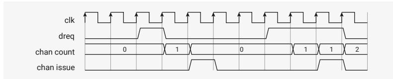
The diagram illustrates the DREQ counting mechanism. It shows four signals over time: clk (clock), dreq (data request), chan count (channel count), and chan issue (channel issue). The clk signal is a regular square wave. The dreq signal is a pulse that occurs at specific clock cycles. The chan count signal is a counter that increments from 0 to 2 as dreq pulses occur. The chan issue signal is a pulse that occurs at the end of each chan count increment.
The effect is to upper bound the number of in-flight transfers based on the amount of room or data available in the peripheral FIFO. In the steady state, this gives maximum throughput, but can't underflow or underflow. This approach has the following caveats:
- • The user must not access a FIFO currently being serviced by the DMA. This causes the channel and peripheral to become desynchronised, and can cause corruption or loss of data.
- • Multiple channels must not be connected to the same DREQ.
12.6.5. Interrupts
Each channel can generate interrupts; these can be masked on a per-channel basis using one of the four identical interrupt enable registers, INTE0 through INTE3 . There are three circumstances where a channel raises an interrupt request:
- • On the completion of each transfer sequence, if CTRL.IRQ_QUIET is disabled
- • On receiving a null trigger, if CTRL.IRQ_QUIET is enabled
- • On a read or write bus error
The masked interrupt status is visible in the INTS registers; there is one bit for each channel. Interrupts are cleared by writing a bit mask to INTS . One idiom for acknowledging interrupts is to read INTS , then write the same value back, so only enabled interrupts are cleared.
The RP2350 DMA provides four system IRQs, with independent masking and status registers (e.g. INTE0 , INTE1 ). Any combination of channel interrupt requests can be routed to each system IRQ, though generally software only routes each channel interrupt to a single system IRQ. For example:
- • Some channels can be given a higher priority in the system interrupt controller, if they have particularly tight timing requirements.
- • In multiprocessor systems, different channel interrupts can be routed independently to different cores.
- • When channels are assigned to a mixture of security domains, IRQs can also be assigned, so that software in each security domain can get interrupts from its own channels.
For debugging purposes, the INTF registers can force any channel interrupt to be asserted, which will cause assertion of any system IRQs that have that channel interrupt's enable bit set in their respective INTE registers.
12.6.6. Security
RP2350's processors support partitioning of memory and peripherals into multiple security domains. This partitioning is extended into the DMA, so that different security contexts can safely use their assigned channels without breaking any of the security invariants laid out by the processor security model. For example, an Arm processor in the Non-secure state must not be able to use the DMA to access memory or peripherals owned by Secure software.
The DMA defines four security levels that map onto Arm or RISC-V processor security states:
- •
3
: SP (secure and privileged)
- ◦ Equivalent to Arm processors in the Secure, Privileged state
- ◦ Equivalent to RISC-V processors in Machine mode
- • 2 : SU (secure and unprivileged)
- ◦ Equivalent to Arm processors in the Secure, Normal state
- • 1: NSP (nonsecure and privileged)
- ◦ Equivalent to Arm processors in the Non-secure, Privileged state
- ◦ Equivalent to RISC-V processors in Supervisor mode
- • 0: NSU (nonsecure and unprivileged)
- ◦ Equivalent to Arm processors in the Non-secure, Normal state
- ◦ Equivalent to RISC-V processors in User mode
So that the DMA can compare different security levels in a consistent way, they are considered ordered, with \( SP > SU > NSP > NSU \) . For example, when we say that a channel requires a minimum of SU to access its registers, this means that SP and SU are acceptable, and NSP and NSU are not. As a rule, every action has a reaction that is at or below the security level of the original action, and so the DMA can not be used to escalate accesses to a higher security level.
Software assigns internal DMA resources, like channels, interrupts, pacing timers and the CRC sniffer, to one of the four possible security levels. These resources are then accessible only at and above that level. Channel assignment in particular is discussed in Section 12.6.6.1 .
The DMA memory protection unit ( Section 12.6.6.3 ) defines the minimum security level required to access up to eight programmable address ranges, so that channels of a given security level can not access memory beyond their means. This MPU is intended to mirror the SRAM and XIP memory protection boundaries configured in the processor SAU or PMP. In addition to the internal filtering performed by the DMA MPU, accesses are filtered by the system bus according to the ACCESSCTRL filter rules described in Section 10.6.2 .
The combination of these features allows the DMA to be safely shared by software running in different security domains. If this is not desired, the entire DMA block can instead be assigned wholesale to a single security domain using the ACCESSCTRL DMA register.
12.6.6.1. Channel security assignment
Channels are assigned to security domains using the channel SECCFG registers, SECCFG_CH0 through SECCFG_CH15 . There is one register per channel. Each register contains a 2-bit security level, and a lock bit that prevents that SECCFG register from being changed once configured. At reset, all channels are assigned to the SP security level, which is the highest.
The security level of a channel defines:
- • The security level of bus transfers performed by this channel, which is checked against both the DMA memory protection unit and the ACCESSCTRL bus-level filters described in Section 10.6.2 .
- • The minimum security level required to read or write this channel's registers; access from a lower level returns a bus fault.
- • The minimum security level that must be defined on a shared IRQ line for that IRQ to be able to observe this channel's interrupts ( Section 12.6.6.2 ), or for this channel's interrupt to be set/cleared through that IRQ's registers.
- • The minimum bus security level required to clear this channel's interrupts through the INTR register.
- • Which DREQs a channel can observe: channels assigned to the NSP or NSU security levels can not observe DREQs of Secure-only peripherals (as defined by the ACCESSCTRL peripheral configuration).
- • Which pacing timer TREQs can be observed; pacing timer security levels are configured by SECCFG_MISC and must be no higher than the channel security level for the channel in order to observe the TREQ.
- • Whether the channel is visible to the CRC sniffer; the sniffer's security level is configured by SECCFG_MISC and must be no lower than the observed channel's security level.
- • Which channels this channel can trigger with a CHAIN_TO ; chaining from lower to higher security levels is not permitted.
- • The minimum bus security level required to trigger this channel with a write to MULTI_CHAN_TRIGGER .
The channel SECCFG registers require privileged writes (SP/NSP), and will generate a bus fault on an attempted unprivileged write (SU/NSU). Additionally, the S bit (MSB of the security level) and the LOCK bit are writable only by SP, whilst the P bit (LSB of the security level) is also writable by NSP, if and only if the S bit is clear. Reads are always allowed: it is always possible to query which channels are assigned to you by reading the channel SECCFG registers.
Each channel SECCFG register can be locked manually by writing a one to the LOCK bit in that register, and will also lock automatically upon a successful write to one of the channel's control registers such as CHO_CTRL_TRIG . This automatic locking avoids any race conditions that can arise from a channel's security level changing after it has already started making transfers, or from leaking secure pointers that have been written to its control registers. After a channel SECCFG register has been locked, it becomes read-only. LOCK bits can be cleared only by a full reset of the DMA block.
SECCFG registers can be written multiple times before being locked, so the full assignment does not have to be known up front: for example, Secure Arm software can set spare channels to NSP before launching the Non-secure software context, and Non-secure, Privileged software can then set the remaining channels it does not need to NSU before returning to the Non-secure, Normal context.
12.6.6.2. Interrupt Security Assignment
The RP2350 DMA has four system-level interrupt request lines (IRQs), each of which can be asserted on any combination of channel interrupts, as defined by the channel masks in the interrupt enable registers INTE0 through INTE3 . Because the timing of interrupts can leak information, and because it is possible to cause software to malfunction by deliberately manipulating its interrupts, access to the channel interrupt flags must be controlled.
The interrupt security configuration registers, SECCFG_IRQ0 through SECCFG_IRQ3 , define the security level for each interrupt. This is one of the four security levels laid out in Section 12.6.6 . The security level of an IRQ defines:
- • Which channels are visible in this IRQ's status registers; channels of a level higher than the IRQ's will read back as zero.
- • Whether a bus access to this IRQ's control and status registers is permitted; bus accesses below this IRQ's security level will return bus faults and have no effect on the DMA.
- • Which channels will assert this IRQ; channels of a level higher than this IRQ's level will not cause the interrupt to assert, even if relevant INTE bit is set.
- • Whether a channel's interrupt can be cleared through this IRQ's INTS register, or set through this channel's INTF register; the interrupt flags of channels of higher security level than the IRQ can not be set or cleared.
The INTR register is shared between all IRQs, so it does not respect any of the IRQ security levels. Instead, it follows the security level of the bus access: reads of INTR will return the interrupt flags of all channels at or below the security level of the bus access (with higher-level channels reading back as zeroes), and writes to INTR have write-one-clear behaviour on channels which are at or below the security level of the bus access.
12.6.6.3. Memory protection unit
The DMA memory protection unit (MPU) monitors the addresses of all read/write transfers performed by the DMA, and notes the security level of the originating channel. The MPU is configured in advance with a user-defined security address map, which specifies the minimum security level required to access up to eight dynamically configured regions. This is one of the four security levels defined in Section 12.6.6 .
Transfers that fail to meet the minimum security level for their address are shot down before reaching the system bus, and a bus error is returned to the originating channel. This will be reported as either a read or write bus error in the channel's CTRL register, depending on whether it was a read or write address that failed the security check.
The intended use for the DMA MPU is to mirror the security definitions of SRAM and XIP memory from the processor SAU or PMP. The number of DMA MPU regions is not sufficient for assigning individual peripherals, so the ACCESSCTRL bus access registers ( Section 10.6.2 ) are provided for this purpose.
Each of the eight MPU regions is configured with a base address, MPU_BAR0 through MPU_BAR7 for each region, and a limit address, MPU_LAR0 through MPU_LAR7 .
MPU regions have a granularity of 32 bytes, so the base/limit addresses are configured by the 27 most-significant bits of each
BAR/LAR
register (bits 31:5). Addresses match MPU regions when the 27 most-significant bits of the address are greater than or equal to the
BAR
address bits, and less than or equal to the
LAR
address bits. For example, when
MPU_BAR0
and
MPU_LAR0
both have the value
0x10000000
, MPU region 0 matches on a 32-byte region extending from byte address
0x10000000
to
0x1000001f
(inclusive). Regions can be enabled or disabled using the
LAR.EN
bits – if a region is disabled, it matches no addresses.
The minimum security level required to access each region is defined by the S and P bits in the LSBs of that region's LAR register. When an address matches multiple regions, the lowest-numbered region applies. This matches the tie-break rules for the RISC-V PMP, but is different from the Arm SAU tie-break rules, so care must be taken when mirroring SAU mappings with overlapping regions. When none of the MPU regions are matched, the security level is defined by the global MPU_CTRL.S and MPU_CTRL.P bits.
The MPU configuration registers ( MPU_CTRL , MPU_BAR0 through MPU_BAR7 and MPU_LAR0 through MPU_LAR7 ) do not permit unprivileged access. Bus accesses at the SU and NSU security levels will return a bus fault and have no other effect.
The MPU registers are also mostly read-only to NSP accesses, with the sole exception being the region P bits which are NSP-writable if and only if the corresponding region's S bit is clear. This delegates to Privileged, Non-secure software the decision of whether Non-secure regions are NSU-accessible.
12.6.7. Bus error handling
A bus error is an error condition flagged to one of the DMA's manager ports in response to an attempted read or write transfer, indicating the transfer was rejected for one of the following reasons:
- • The DMA MPU forbids access to this address at the originating channel's security level ( Section 12.6.6.3 ).
- • The bus fabric failed to decode the address; the address did not match any known memory location (for example SIO is not visible from the DMA bus ports as it is tightly coupled to the processors).
- • ACCESSCTRL forbids access to the addressed region at the originating channel's privilege level ( Section 10.6.2 ).
- • ACCESSCTRL forbids DMA access to the addressed region, irrespective of privilege.
- • The APB bridge returned a timeout fault for a transfer exceeding 65535 cycles (e.g. accessed ADC whilst clk_adc was stopped).
- • The downstream bus port returned an error response for any other device-specific reason, e.g. attempting to access configuration registers for a DMA channel with higher security level ( Section 12.6.6.1 ).
12.6.7.1. Response to bus errors
Upon encountering a bus error, the DMA halts the offending channel and reports the error through the channel's CH0_CTRL.TRIG.READ_ERROR and WRITE_ERROR flags. The channel stops scheduling bus accesses.
Bus errors are exceptional events which usually indicate misconfiguration of the DMA or some other system hardware. Therefore the DMA refuses to restart the offending channel until its error status is cleared by writing
1
to the relevant error flag. Other channels are not affected, and continue their transfer sequences uninterrupted.
A channel which encounters a bus error does not CHAIN_TO other channels.
Bus errors always cause the channel's interrupt request to be asserted. Whether or not this causes a system-level IRQ depends on the channel masks configured in interrupt enable registers INTE0 through INTE3 .
12.6.7.2. Recovery after bus errors
If an error is reported through
READ_ERR
/
WRITE_ERR
then, before restarting the channel, software must:
- 1. Poll for a low
BUSYstatus to ensure that all in-flight transfers for this channel have been flushed from the DMA's bus pipeline. - 2. Clear the error flags by writing
1to each flag.
Generally the
BUSY
flag will already be low long before the processor enters its interrupt handler and checks the error status, but it is possible for these events to overlap when the DMA is accessing a slow device such as XIP with a high
SCK
divisor and processors are executing from SRAM.
READ_ADDR
and
WRITE_ADDR
contain the approximate address where the bus error was encountered. This can be useful for the programmer to understand why the bus error occurred, and fix the software to avoid it in future.
Since the DMA performs reads and writes in parallel, it is possible for a channel to encounter both a read and write error simultaneously, and in this case the DMA sets both
READ_ERR
and
WRITE_ERR
. You must clear both.
12.6.7.3. Halt timing
The DMA halts the channel as soon as possible following a bus error. This suppresses future reads and writes. Because the request to access the bus is masked, the bus access has no side effects on the system. The timing relationships are not straightforward due to the DMA's pipelining and buffering. The DMA provides the following ordering guarantees between transfers originating from one channel:
- • Read error → read suppression: Any reads scheduled to occur after a faulting read
will
be suppressed, but
can
still increment
READ_ADDRup to two times total - • Write error → write suppression: Any writes scheduled to occur after a faulting write
will
be suppressed, but
can
still increment
WRITE_ADDRup to four times total - • Read error → write suppression:
- ◦ Any write paired with a faulting read
will
be suppressed, but
will
increment
WRITE_ADDR - ◦ Any write following the first write paired with a faulting read
will
be suppressed, but
can
increment
WRITE_ADDRup to three times total - ◦ Up to three writes immediately preceding the first write paired with a faulting read
can
be suppressed, but
will
increment
WRITE_ADDR
- ◦ Any write paired with a faulting read
will
be suppressed, but
will
increment
- • Write error → read suppression:
- ◦ Reads paired with writes before the first faulting write
will not
be suppressed, and
will
increment
READ_ADDR. - ◦ Up to two read transfers paired with writes after the first faulting write
can
be suppressed, and
can
increment
READ_ADDR
- ◦ Reads paired with writes before the first faulting write
will not
be suppressed, and
will
increment
"Paired with" in the above paragraph refers to the write access which writes data originating from a particular read transfer , or vice versa. The DMA always schedules read and write accesses in matched pairs.
Slight variability in halt behaviour is due to the buffering of in-flight transfers, and the parallel operation of the read and write bus ports. The values of
READ_ADDR
/
WRITE_ADDR
following a bus error can be slightly beyond the address that experienced the first error, but the difference is bounded, and usually this is still sufficient to diagnose the reason for the fault. Additionally,
READ_ADDR
and
WRITE_ADDR
are guaranteed to over-increment by the same amount, since reads and writes are always scheduled in pairs.
In addition to the increments mentioned above,
READ_ADDR
/
WRITE_ADDR
always point to the
next
address to be written, so always point slightly past the faulting address if address increment is enabled.
12.6.8. Additional features
12.6.8.1. Pacing timers
These allow transfer of data roughly once every
\(
n
\)
clk_sys
clocks instead of using external peripheral DREQ to trigger transfers. A fractional (X/Y) divider is used, and will generate a maximum of 1 request per
clk_sys
cycle.
There are 4 timers available in RP2350. Each DMA channel is able to select any of these in
CTRL.TREQ_SEL
. There is one register used to configure the pacing coefficients for each timer,
TIMER0
through
TIMER3
.
Each timer's security level is defined by a register field in
SECCFG_MISC
. This defines the minimum bus security level required to configure that timer (lower levels will get a bus fault), and the minimum channel security level required to observe that timer's TREQ.
12.6.8.2. CRC calculation
The DMA can watch data from a given channel passing through the data FIFO, and calculate checksums based on this data. This is a purely passive affair: the data is not altered by this hardware, only observed.
The feature is controlled via the
SNIFF_CTRL
and
SNIFF_DATA
registers, and can be enabled/disabled per DMA transfer via the
CTRL.SNIFF_EN
field.
As this hardware cannot place back-pressure on the FIFO, it must keep up with the DMA's maximum transfer rate of 32 bits per clock.
The supported checksums are:
- • CRC-32, MSB-first and LSB-first
- • CRC-16-CCITT, MSB-first and LSB-first
- • Simple summation (add to 32-bit accumulator)
- • Even parity
The result register is both readable and writable, so that the initial seed value can be set.
Bit/byte manipulations are available on the result, which can aid specific use cases:
- • Bit inversion
- • Bit reversal
- • Byte swap
These manipulations do not affect the CRC calculation, just how the data is presented in the result register.
The sniffer's security level is configured by the
SECCFG_MISC.SNIFF_S
and
SECCFG_MISC.SNIFF_P
bits. This determines the minimum bus security level required to access the sniffer's control registers, as well as the maximum channel security level that the sniffer can observe.
12.6.8.3. Channel abort
It is possible for a channel to get into an irrecoverable state. If commanded to transfer more data than a peripheral will ever request, the channel will never complete. Clearing the
CTRL.EN
bit pauses the channel, but does not solve the problem. This should not occur under normal circumstances, but it is important that there is a mechanism to recover without simply hard-resetting the entire DMA block.
In such a situation, use the
CHAN_ABORT
register to force the channel to complete early. There is one bit for each channel. Writing a 1 to the corresponding bit terminates the channel. This clears the transfer counter and forces the channel into an inactive state.
At the time an abort is triggered, a channel might have bus transfers currently in flight between the read and write manager. These transfers cannot be revoked. The
CTRL.BUSY
flag stays high until these transfers complete, and the channel reaches a safe state. This generally takes only a few cycles. The channel must not be restarted until its
CTRL.BUSY
flag de-asserts. Starting a new sequence of transfers whilst transfers from an old sequence are still in flight will cause unpredictable behaviour.
The sequence to abort one or more channels in an unknown state (also accounting for the behaviour described in RP2350-E5 is:
- 1. Clear the
ENbit and disableCHAIN_TOfor all channels to be aborted. - 2. Write the
CHAN_ABORTregister with a bitmap of those same channels. - 3. Poll the
ABORTregister until all bits set by the previous write are clear.
When aborting a channel involved in a
CHAIN_TO
, it is recommended to simultaneously abort all other channels involved in the chain.
12.6.8.4. Debug
Debug registers are available for each DMA channel to show the dreq counter
DBG_CTDREQ
and next transfer count
DBG_TCR
. These can also be used to reset a DMA channel if required.
12.6.9. Example use cases
12.6.9.1. Using interrupts to reconfigure a channel
When a channel finishes a block of transfers, it becomes available for making more transfers. Software detects that the channel is no longer busy, and reconfigures and restarts the channel. One approach is to poll the
CTRL_BUSY
bit until the channel is done, but this loses one of the key advantages of the DMA, namely that it does
not
have to operate in lockstep with a processor. By setting the correct bit in
INTE0
through
INTE3
, you can instruct the DMA to raise one of its four interrupt request lines when a given channel completes. Rather than repeatedly asking if a channel is done, you are told.
i NOTE
Having four system interrupt lines allows different channel completion interrupts to be routed to different cores, or to pre-empt one another on the same core if one channel is more time-critical. It also allows channel interrupts to target different security domains.
When the interrupt is asserted, the processor can be configured to drop whatever it is doing and call a user-specified handler function. The handler can reconfigure and restart the channel. When the handler exits, the processor returns to the interrupted code running in the foreground.
Pico Examples: https://github.com/raspberrypi/pico-examples/blob/master/dma/channel_irq/channel_irq.c Lines 35 - 52
35 void dma_handler() {
36     static int pwm_level = 0;
37     static uint32_t wavetable[N_PWM_LEVELS];
38     static bool first_run = true;
39     // Entry number `i` has `i` one bits and `(32 - i)` zero bits.
40     if (first_run) {
41         first_run = false;
42         for (int i = 0; i < N_PWM_LEVELS; ++i)
43             wavetable[i] = ~(~0u << i);
44     }
45 }
46 // Clear the interrupt request. 47 dma_hw->ints0 = 1u << dma_chan; 48 // Give the channel a new wave table entry to read from, and re-trigger it 49 dma_channel_set_read_addr(dma_chan, &wavetable[pwm_level], true); 50 51 pwm_level = (pwm_level + 1) % N_PWM_LEVELS; 52 }
In many cases, most of the configuration can be done the first time the channel starts. This way, only addresses and transfer lengths need reprogramming in the interrupt handler.
Pico Examples: https://github.com/raspberrypi/pico-examples/blob/master/dma/channel_irq/channel_irq.c Lines 54 - 94
54 int main() {
55 #ifndef PICO_DEFAULT_LED_PIN
56 #warning dma/channel_irq example requires a board with a regular LED
57 #else
58 // Set up a PIO state machine to serialise our bits
59 uint offset = pio_add_program(pio0, &pio_serialiser_program);
60 pio_serialiser_program_init(pio0, 0, offset, PICO_DEFAULT_LED_PIN, PIO_SERIAL_CLKDIV);
61
62 // Configure a channel to write the same word (32 bits) repeatedly to PIO0
63 // SM0's TX FIFO, paced by the data request signal from that peripheral.
64 dma_chan = dma_claim_unused_channel(true);
65 dma_channel_config c = dma_channel_get_default_config(dma_chan);
66 channel_config_set_transfer_data_size(&c, DMA_SIZE_32);
67 channel_config_set_read_increment(&c, false);
68 channel_config_set_dreq(&c, DREQ_PIO0_TX0);
69
70 dma_channel_configure(
71     dma_chan,
72     &c,
73     &pio0_hw->txf[0], // Write address (only need to set this once)
74     NULL,             // Don't provide a read address yet
75     PWM_REPEAT_COUNT, // Write the same value many times, then halt and interrupt
76     false             // Don't start yet
77 );
78
79 // Tell the DMA to raise IRQ line 0 when the channel finishes a block
80 dma_channel_set_irq0_enabled(dma_chan, true);
81
82 // Configure the processor to run dma_handler() when DMA IRQ 0 is asserted
83 irq_set_exclusive_handler(DMA_IRQ_0, dma_handler);
84 irq_set_enabled(DMA_IRQ_0, true);
85
86 // Manually call the handler once, to trigger the first transfer
87 dma_handler();
88
89 // Everything else from this point is interrupt-driven. The processor has
90 // time to sit and think about its early retirement -- maybe open a bakery?
91 while (true)
92     tight_loop_contents();
93 #endif
94 }
One disadvantage of this technique is that you don't start to reconfigure the channel until some time after the channel makes its last transfer. If there is heavy interrupt activity on the processor, this can be quite a long time, and quite a large gap in transfers. This makes it difficult to sustain a high data throughput.
This is solved by using two channels, with their
CHAIN_TO
fields crossed over, so that channel A triggers channel B when it completes, and vice versa. At any point in time, one of the channels is transferring data. The other is either already
configured to start the next transfer immediately when the current one finishes, or it is in the process of being reconfigured. When channel A completes, it immediately starts the cued-up transfer on channel B. At the same time, the interrupt is fired, and the handler reconfigures channel A so that it is ready when channel B completes.
12.6.9.2. DMA control blocks
Frequently, multiple smaller buffers must be gathered together and sent to the same peripheral. To address this use case, the RP2350 DMA can execute a long and complex sequence of transfers without processor control. One channel repeatedly reconfigures a second channel, and the second channel restarts the first each time it completes block of transfers.
Because the first DMA channel transfers data directly from memory to the second channel's control registers, the format of the control blocks in memory must match those registers. Each time, the last register written to will be one of the trigger registers (Section 12.6.3.1), which will start the second channel on its programmed block of transfers. The register aliases (Section 12.6.3.1) give some flexibility for the block layout, and more importantly allow some registers to be omitted from the blocks, so they occupy less memory and can be loaded more quickly.
This example shows how multiple buffers can be gathered and transferred to the UART, by reprogramming
TRANS_COUNT
and
READ_ADDR_TRIG
:
Pico Examples: https://github.com/raspberrypi/pico-examples/blob/master/dma/control_blocks/control_blocks.c
1  /**
2   * Copyright (c) 2020 Raspberry Pi (Trading) Ltd.
3   *
4   * SPDX-License-Identifier: BSD-3-Clause
5   */
6
7  // Use two DMA channels to make a programmed sequence of data transfers to the
8  // UART (a data gather operation). One channel is responsible for transferring
9  // the actual data, the other repeatedly reprograms that channel.
10
11 #include <stdio.h>
12 #include "pico/stdlib.h"
13 #include "hardware/dma.h"
14 #include "hardware/structs/uart.h"
15
16 // These buffers will be DMA'd to the UART, one after the other.
17
18 const char word0[] = "Transferring ";
19 const char word1[] = "one ";
20 const char word2[] = "word ";
21 const char word3[] = "at ";
22 const char word4[] = "a ";
23 const char word5[] = "time.\n";
24
25 // Note the order of the fields here: it's important that the length is before
26 // the read address, because the control channel is going to write to the last
27 // two registers in alias 3 on the data channel:
28 //          +0x0      +0x4      +0x8      +0xC (Trigger)
29 // Alias 0:  READ_ADDR  WRITE_ADDR  TRANS_COUNT  CTRL
30 // Alias 1:  CTRL      READ_ADDR  WRITE_ADDR  TRANS_COUNT
31 // Alias 2:  CTRL      TRANS_COUNT  READ_ADDR  WRITE_ADDR
32 // Alias 3:  CTRL      WRITE_ADDR  TRANS_COUNT  READ_ADDR
33 //
34 // This will program the transfer count and read address of the data channel,
35 // and trigger it. Once the data channel completes, it will restart the
36 // control channel (via CHAIN_TO) to load the next two words into its control
37 // registers.
38
39 const struct {uint32_t len; const char *data;} control_blocks[] = {
40     {count_of(word0) - 1, word0}, // Skip null terminator
41     {count_of(word1) - 1, word1},
42     {count_of(word2) - 1, word2},
43     {count_of(word3) - 1, word3},
44     {count_of(word4) - 1, word4},
45     {count_of(word5) - 1, word5},
46     {0, NULL} // Null trigger to end chain.
47 };
48
49 int main() {
50 #ifndef uart_default
51 #warning dma/control_blocks example requires a UART
52 #else
53     stdio_init_all();
54     puts("DMA control block example:");
55
56     // ctrl_chan loads control blocks into data_chan, which executes them.
57     int ctrl_chan = dma_claim_unused_channel(true);
58     int data_chan = dma_claim_unused_channel(true);
59
60     // The control channel transfers two words into the data channel's control
61     // registers, then halts. The write address wraps on a two-word
62     // (eight-byte) boundary, so that the control channel writes the same two
63     // registers when it is next triggered.
64
65     dma_channel_config c = dma_channel_get_default_config(ctrl_chan);
66     channel_config_set_transfer_data_size(&c, DMA_SIZE_32);
67     channel_config_set_read_increment(&c, true);
68     channel_config_set_write_increment(&c, true);
69     channel_config_set_ring(&c, true, 3); // 1 << 3 byte boundary on write ptr
70
71     dma_channel_configure(
72         ctrl_chan,
73         &c,
74         &dma_hw->ch[data_chan].al3_transfer_count, // Initial write address
75         &control_blocks[0], // Initial read address
76         2, // Halt after each control block
77         false // Don't start yet
78     );
79
80     // The data channel is set up to write to the UART FIFO (paced by the
81     // UART's TX data request signal) and then chain to the control channel
82     // once it completes. The control channel programs a new read address and
83     // data length, and retriggers the data channel.
84
85     c = dma_channel_get_default_config(data_chan);
86     channel_config_set_transfer_data_size(&c, DMA_SIZE_8);
87     channel_config_set_dreq(&c, uart_get_dreq(uart_default, true));
88     // Trigger ctrl_chan when data_chan completes
89     channel_config_set_chain_to(&c, ctrl_chan);
90     // Raise the IRQ flag when 0 is written to a trigger register (end of chain):
91     channel_config_set_irq_quiet(&c, true);
92
93     dma_channel_configure(
94         data_chan,
95         &c,
96         &uart_get_hw(uart_default)->dr,
97         NULL, // Initial read address and transfer count are unimportant;
98         0, // the control channel will reprogram them each time.
99         false // Don't start yet.
100    );
101
102    // Everything is ready to go. Tell the control channel to load the first
103    // control block. Everything is automatic from here.
104 dma_start_channel_mask(1u << ctrl_chan);
105
106 // The data channel will assert its IRQ flag when it gets a null trigger,
107 // indicating the end of the control block list. We're just going to wait
108 // for the IRQ flag instead of setting up an interrupt handler.
109 while (!(dma_hw->intr & 1u << data_chan))
110     tight_loop_contents();
111 dma_hw->ints0 = 1u << data_chan;
112
113 puts("DMA finished.");
114 #endif
115 }
12.6.10. List of Registers
The DMA registers start at a base address of 0x50000000 (defined as DMA_BASE in SDK).
Table 1147. List of DMA registers
| Offset | Name | Info |
|---|---|---|
| 0x000 | CH0_READ_ADDR | DMA Channel 0 Read Address pointer |
| 0x004 | CH0_WRITE_ADDR | DMA Channel 0 Write Address pointer |
| 0x008 | CH0_TRANS_COUNT | DMA Channel 0 Transfer Count |
| 0x00c | CH0_CTRL_TRIG | DMA Channel 0 Control and Status |
| 0x010 | CH0_AL1_CTRL | Alias for channel 0 CTRL register |
| 0x014 | CH0_AL1_READ_ADDR | Alias for channel 0 READ_ADDR register |
| 0x018 | CH0_AL1_WRITE_ADDR | Alias for channel 0 WRITE_ADDR register |
| 0x01c | CH0_AL1_TRANS_COUNT_TRIG | Alias for channel 0 TRANS_COUNT register This is a trigger register (0xc). Writing a nonzero value will reload the channel counter and start the channel. |
| 0x020 | CH0_AL2_CTRL | Alias for channel 0 CTRL register |
| 0x024 | CH0_AL2_TRANS_COUNT | Alias for channel 0 TRANS_COUNT register |
| 0x028 | CH0_AL2_READ_ADDR | Alias for channel 0 READ_ADDR register |
| 0x02c | CH0_AL2_WRITE_ADDR_TRIG | Alias for channel 0 WRITE_ADDR register This is a trigger register (0xc). Writing a nonzero value will reload the channel counter and start the channel. |
| 0x030 | CH0_AL3_CTRL | Alias for channel 0 CTRL register |
| 0x034 | CH0_AL3_WRITE_ADDR | Alias for channel 0 WRITE_ADDR register |
| 0x038 | CH0_AL3_TRANS_COUNT | Alias for channel 0 TRANS_COUNT register |
| 0x03c | CH0_AL3_READ_ADDR_TRIG | Alias for channel 0 READ_ADDR register This is a trigger register (0xc). Writing a nonzero value will reload the channel counter and start the channel. |
| 0x040 | CH1_READ_ADDR | DMA Channel 1 Read Address pointer |
| 0x044 | CH1_WRITE_ADDR | DMA Channel 1 Write Address pointer |
| 0x048 | CH1_TRANS_COUNT | DMA Channel 1 Transfer Count |
| 0x04c | CH1_CTRL_TRIG | DMA Channel 1 Control and Status |
| Offset | Name | Info |
|---|---|---|
| 0x050 | CH1_AL1_CTRL | Alias for channel 1 CTRL register |
| 0x054 | CH1_AL1_READ_ADDR | Alias for channel 1 READ_ADDR register |
| 0x058 | CH1_AL1_WRITE_ADDR | Alias for channel 1 WRITE_ADDR register |
| 0x05c | CH1_AL1_TRANS_COUNT_TRIG | Alias for channel 1 TRANS_COUNT register This is a trigger register (0xc). Writing a nonzero value will reload the channel counter and start the channel. |
| 0x060 | CH1_AL2_CTRL | Alias for channel 1 CTRL register |
| 0x064 | CH1_AL2_TRANS_COUNT | Alias for channel 1 TRANS_COUNT register |
| 0x068 | CH1_AL2_READ_ADDR | Alias for channel 1 READ_ADDR register |
| 0x06c | CH1_AL2_WRITE_ADDR_TRIG | Alias for channel 1 WRITE_ADDR register This is a trigger register (0xc). Writing a nonzero value will reload the channel counter and start the channel. |
| 0x070 | CH1_AL3_CTRL | Alias for channel 1 CTRL register |
| 0x074 | CH1_AL3_WRITE_ADDR | Alias for channel 1 WRITE_ADDR register |
| 0x078 | CH1_AL3_TRANS_COUNT | Alias for channel 1 TRANS_COUNT register |
| 0x07c | CH1_AL3_READ_ADDR_TRIG | Alias for channel 1 READ_ADDR register This is a trigger register (0xc). Writing a nonzero value will reload the channel counter and start the channel. |
| 0x080 | CH2_READ_ADDR | DMA Channel 2 Read Address pointer |
| 0x084 | CH2_WRITE_ADDR | DMA Channel 2 Write Address pointer |
| 0x088 | CH2_TRANS_COUNT | DMA Channel 2 Transfer Count |
| 0x08c | CH2_CTRL_TRIG | DMA Channel 2 Control and Status |
| 0x090 | CH2_AL1_CTRL | Alias for channel 2 CTRL register |
| 0x094 | CH2_AL1_READ_ADDR | Alias for channel 2 READ_ADDR register |
| 0x098 | CH2_AL1_WRITE_ADDR | Alias for channel 2 WRITE_ADDR register |
| 0x09c | CH2_AL1_TRANS_COUNT_TRIG | Alias for channel 2 TRANS_COUNT register This is a trigger register (0xc). Writing a nonzero value will reload the channel counter and start the channel. |
| 0x0a0 | CH2_AL2_CTRL | Alias for channel 2 CTRL register |
| 0x0a4 | CH2_AL2_TRANS_COUNT | Alias for channel 2 TRANS_COUNT register |
| 0x0a8 | CH2_AL2_READ_ADDR | Alias for channel 2 READ_ADDR register |
| 0x0ac | CH2_AL2_WRITE_ADDR_TRIG | Alias for channel 2 WRITE_ADDR register This is a trigger register (0xc). Writing a nonzero value will reload the channel counter and start the channel. |
| 0x0b0 | CH2_AL3_CTRL | Alias for channel 2 CTRL register |
| 0x0b4 | CH2_AL3_WRITE_ADDR | Alias for channel 2 WRITE_ADDR register |
| 0x0b8 | CH2_AL3_TRANS_COUNT | Alias for channel 2 TRANS_COUNT register |
| 0x0bc | CH2_AL3_READ_ADDR_TRIG | Alias for channel 2 READ_ADDR register This is a trigger register (0xc). Writing a nonzero value will reload the channel counter and start the channel. |
| Offset | Name | Info |
|---|---|---|
| 0x0c0 | CH3_READ_ADDR | DMA Channel 3 Read Address pointer |
| 0x0c4 | CH3_WRITE_ADDR | DMA Channel 3 Write Address pointer |
| 0x0c8 | CH3_TRANS_COUNT | DMA Channel 3 Transfer Count |
| 0x0cc | CH3_CTRL_TRIG | DMA Channel 3 Control and Status |
| 0x0d0 | CH3_AL1_CTRL | Alias for channel 3 CTRL register |
| 0x0d4 | CH3_AL1_READ_ADDR | Alias for channel 3 READ_ADDR register |
| 0x0d8 | CH3_AL1_WRITE_ADDR | Alias for channel 3 WRITE_ADDR register |
| 0x0dc | CH3_AL1_TRANS_COUNT_TRIG | Alias for channel 3 TRANS_COUNT register This is a trigger register (0xc). Writing a nonzero value will reload the channel counter and start the channel. |
| 0x0e0 | CH3_AL2_CTRL | Alias for channel 3 CTRL register |
| 0x0e4 | CH3_AL2_TRANS_COUNT | Alias for channel 3 TRANS_COUNT register |
| 0x0e8 | CH3_AL2_READ_ADDR | Alias for channel 3 READ_ADDR register |
| 0x0ec | CH3_AL2_WRITE_ADDR_TRIG | Alias for channel 3 WRITE_ADDR register This is a trigger register (0xc). Writing a nonzero value will reload the channel counter and start the channel. |
| 0x0f0 | CH3_AL3_CTRL | Alias for channel 3 CTRL register |
| 0x0f4 | CH3_AL3_WRITE_ADDR | Alias for channel 3 WRITE_ADDR register |
| 0x0f8 | CH3_AL3_TRANS_COUNT | Alias for channel 3 TRANS_COUNT register |
| 0x0fc | CH3_AL3_READ_ADDR_TRIG | Alias for channel 3 READ_ADDR register This is a trigger register (0xc). Writing a nonzero value will reload the channel counter and start the channel. |
| 0x100 | CH4_READ_ADDR | DMA Channel 4 Read Address pointer |
| 0x104 | CH4_WRITE_ADDR | DMA Channel 4 Write Address pointer |
| 0x108 | CH4_TRANS_COUNT | DMA Channel 4 Transfer Count |
| 0x10c | CH4_CTRL_TRIG | DMA Channel 4 Control and Status |
| 0x110 | CH4_AL1_CTRL | Alias for channel 4 CTRL register |
| 0x114 | CH4_AL1_READ_ADDR | Alias for channel 4 READ_ADDR register |
| 0x118 | CH4_AL1_WRITE_ADDR | Alias for channel 4 WRITE_ADDR register |
| 0x11c | CH4_AL1_TRANS_COUNT_TRIG | Alias for channel 4 TRANS_COUNT register This is a trigger register (0xc). Writing a nonzero value will reload the channel counter and start the channel. |
| 0x120 | CH4_AL2_CTRL | Alias for channel 4 CTRL register |
| 0x124 | CH4_AL2_TRANS_COUNT | Alias for channel 4 TRANS_COUNT register |
| 0x128 | CH4_AL2_READ_ADDR | Alias for channel 4 READ_ADDR register |
| 0x12c | CH4_AL2_WRITE_ADDR_TRIG | Alias for channel 4 WRITE_ADDR register This is a trigger register (0xc). Writing a nonzero value will reload the channel counter and start the channel. |
| 0x130 | CH4_AL3_CTRL | Alias for channel 4 CTRL register |
| Offset | Name | Info |
|---|---|---|
| 0x134 | CH4_AL3_WRITE_ADDR | Alias for channel 4 WRITE_ADDR register |
| 0x138 | CH4_AL3_TRANS_COUNT | Alias for channel 4 TRANS_COUNT register |
| 0x13c | CH4_AL3_READ_ADDR_TRIG | Alias for channel 4 READ_ADDR register This is a trigger register (0xc). Writing a nonzero value will reload the channel counter and start the channel. |
| 0x140 | CH5_READ_ADDR | DMA Channel 5 Read Address pointer |
| 0x144 | CH5_WRITE_ADDR | DMA Channel 5 Write Address pointer |
| 0x148 | CH5_TRANS_COUNT | DMA Channel 5 Transfer Count |
| 0x14c | CH5_CTRL_TRIG | DMA Channel 5 Control and Status |
| 0x150 | CH5_AL1_CTRL | Alias for channel 5 CTRL register |
| 0x154 | CH5_AL1_READ_ADDR | Alias for channel 5 READ_ADDR register |
| 0x158 | CH5_AL1_WRITE_ADDR | Alias for channel 5 WRITE_ADDR register |
| 0x15c | CH5_AL1_TRANS_COUNT_TRIG | Alias for channel 5 TRANS_COUNT register This is a trigger register (0xc). Writing a nonzero value will reload the channel counter and start the channel. |
| 0x160 | CH5_AL2_CTRL | Alias for channel 5 CTRL register |
| 0x164 | CH5_AL2_TRANS_COUNT | Alias for channel 5 TRANS_COUNT register |
| 0x168 | CH5_AL2_READ_ADDR | Alias for channel 5 READ_ADDR register |
| 0x16c | CH5_AL2_WRITE_ADDR_TRIG | Alias for channel 5 WRITE_ADDR register This is a trigger register (0xc). Writing a nonzero value will reload the channel counter and start the channel. |
| 0x170 | CH5_AL3_CTRL | Alias for channel 5 CTRL register |
| 0x174 | CH5_AL3_WRITE_ADDR | Alias for channel 5 WRITE_ADDR register |
| 0x178 | CH5_AL3_TRANS_COUNT | Alias for channel 5 TRANS_COUNT register |
| 0x17c | CH5_AL3_READ_ADDR_TRIG | Alias for channel 5 READ_ADDR register This is a trigger register (0xc). Writing a nonzero value will reload the channel counter and start the channel. |
| 0x180 | CH6_READ_ADDR | DMA Channel 6 Read Address pointer |
| 0x184 | CH6_WRITE_ADDR | DMA Channel 6 Write Address pointer |
| 0x188 | CH6_TRANS_COUNT | DMA Channel 6 Transfer Count |
| 0x18c | CH6_CTRL_TRIG | DMA Channel 6 Control and Status |
| 0x190 | CH6_AL1_CTRL | Alias for channel 6 CTRL register |
| 0x194 | CH6_AL1_READ_ADDR | Alias for channel 6 READ_ADDR register |
| 0x198 | CH6_AL1_WRITE_ADDR | Alias for channel 6 WRITE_ADDR register |
| 0x19c | CH6_AL1_TRANS_COUNT_TRIG | Alias for channel 6 TRANS_COUNT register This is a trigger register (0xc). Writing a nonzero value will reload the channel counter and start the channel. |
| 0x1a0 | CH6_AL2_CTRL | Alias for channel 6 CTRL register |
| 0x1a4 | CH6_AL2_TRANS_COUNT | Alias for channel 6 TRANS_COUNT register |
| Offset | Name | Info |
|---|---|---|
| 0x1a8 | CH6_AL2_READ_ADDR | Alias for channel 6 READ_ADDR register |
| 0x1ac | CH6_AL2_WRITE_ADDR_TRIG | Alias for channel 6 WRITE_ADDR register This is a trigger register (0xc). Writing a nonzero value will reload the channel counter and start the channel. |
| 0x1b0 | CH6_AL3_CTRL | Alias for channel 6 CTRL register |
| 0x1b4 | CH6_AL3_WRITE_ADDR | Alias for channel 6 WRITE_ADDR register |
| 0x1b8 | CH6_AL3_TRANS_COUNT | Alias for channel 6 TRANS_COUNT register |
| 0x1bc | CH6_AL3_READ_ADDR_TRIG | Alias for channel 6 READ_ADDR register This is a trigger register (0xc). Writing a nonzero value will reload the channel counter and start the channel. |
| 0x1c0 | CH7_READ_ADDR | DMA Channel 7 Read Address pointer |
| 0x1c4 | CH7_WRITE_ADDR | DMA Channel 7 Write Address pointer |
| 0x1c8 | CH7_TRANS_COUNT | DMA Channel 7 Transfer Count |
| 0x1cc | CH7_CTRL_TRIG | DMA Channel 7 Control and Status |
| 0x1d0 | CH7_AL1_CTRL | Alias for channel 7 CTRL register |
| 0x1d4 | CH7_AL1_READ_ADDR | Alias for channel 7 READ_ADDR register |
| 0x1d8 | CH7_AL1_WRITE_ADDR | Alias for channel 7 WRITE_ADDR register |
| 0x1dc | CH7_AL1_TRANS_COUNT_TRIG | Alias for channel 7 TRANS_COUNT register This is a trigger register (0xc). Writing a nonzero value will reload the channel counter and start the channel. |
| 0x1e0 | CH7_AL2_CTRL | Alias for channel 7 CTRL register |
| 0x1e4 | CH7_AL2_TRANS_COUNT | Alias for channel 7 TRANS_COUNT register |
| 0x1e8 | CH7_AL2_READ_ADDR | Alias for channel 7 READ_ADDR register |
| 0x1ec | CH7_AL2_WRITE_ADDR_TRIG | Alias for channel 7 WRITE_ADDR register This is a trigger register (0xc). Writing a nonzero value will reload the channel counter and start the channel. |
| 0x1f0 | CH7_AL3_CTRL | Alias for channel 7 CTRL register |
| 0x1f4 | CH7_AL3_WRITE_ADDR | Alias for channel 7 WRITE_ADDR register |
| 0x1f8 | CH7_AL3_TRANS_COUNT | Alias for channel 7 TRANS_COUNT register |
| 0x1fc | CH7_AL3_READ_ADDR_TRIG | Alias for channel 7 READ_ADDR register This is a trigger register (0xc). Writing a nonzero value will reload the channel counter and start the channel. |
| 0x200 | CH8_READ_ADDR | DMA Channel 8 Read Address pointer |
| 0x204 | CH8_WRITE_ADDR | DMA Channel 8 Write Address pointer |
| 0x208 | CH8_TRANS_COUNT | DMA Channel 8 Transfer Count |
| 0x20c | CH8_CTRL_TRIG | DMA Channel 8 Control and Status |
| 0x210 | CH8_AL1_CTRL | Alias for channel 8 CTRL register |
| 0x214 | CH8_AL1_READ_ADDR | Alias for channel 8 READ_ADDR register |
| 0x218 | CH8_AL1_WRITE_ADDR | Alias for channel 8 WRITE_ADDR register |
| Offset | Name | Info |
|---|---|---|
| 0x21c | CH8_AL1_TRANS_COUNT_TRIG | Alias for channel 8 TRANS_COUNT register This is a trigger register (0xc). Writing a nonzero value will reload the channel counter and start the channel. |
| 0x220 | CH8_AL2_CTRL | Alias for channel 8 CTRL register |
| 0x224 | CH8_AL2_TRANS_COUNT | Alias for channel 8 TRANS_COUNT register |
| 0x228 | CH8_AL2_READ_ADDR | Alias for channel 8 READ_ADDR register |
| 0x22c | CH8_AL2_WRITE_ADDR_TRIG | Alias for channel 8 WRITE_ADDR register This is a trigger register (0xc). Writing a nonzero value will reload the channel counter and start the channel. |
| 0x230 | CH8_AL3_CTRL | Alias for channel 8 CTRL register |
| 0x234 | CH8_AL3_WRITE_ADDR | Alias for channel 8 WRITE_ADDR register |
| 0x238 | CH8_AL3_TRANS_COUNT | Alias for channel 8 TRANS_COUNT register |
| 0x23c | CH8_AL3_READ_ADDR_TRIG | Alias for channel 8 READ_ADDR register This is a trigger register (0xc). Writing a nonzero value will reload the channel counter and start the channel. |
| 0x240 | CH9_READ_ADDR | DMA Channel 9 Read Address pointer |
| 0x244 | CH9_WRITE_ADDR | DMA Channel 9 Write Address pointer |
| 0x248 | CH9_TRANS_COUNT | DMA Channel 9 Transfer Count |
| 0x24c | CH9_CTRL_TRIG | DMA Channel 9 Control and Status |
| 0x250 | CH9_AL1_CTRL | Alias for channel 9 CTRL register |
| 0x254 | CH9_AL1_READ_ADDR | Alias for channel 9 READ_ADDR register |
| 0x258 | CH9_AL1_WRITE_ADDR | Alias for channel 9 WRITE_ADDR register |
| 0x25c | CH9_AL1_TRANS_COUNT_TRIG | Alias for channel 9 TRANS_COUNT register This is a trigger register (0xc). Writing a nonzero value will reload the channel counter and start the channel. |
| 0x260 | CH9_AL2_CTRL | Alias for channel 9 CTRL register |
| 0x264 | CH9_AL2_TRANS_COUNT | Alias for channel 9 TRANS_COUNT register |
| 0x268 | CH9_AL2_READ_ADDR | Alias for channel 9 READ_ADDR register |
| 0x26c | CH9_AL2_WRITE_ADDR_TRIG | Alias for channel 9 WRITE_ADDR register This is a trigger register (0xc). Writing a nonzero value will reload the channel counter and start the channel. |
| 0x270 | CH9_AL3_CTRL | Alias for channel 9 CTRL register |
| 0x274 | CH9_AL3_WRITE_ADDR | Alias for channel 9 WRITE_ADDR register |
| 0x278 | CH9_AL3_TRANS_COUNT | Alias for channel 9 TRANS_COUNT register |
| 0x27c | CH9_AL3_READ_ADDR_TRIG | Alias for channel 9 READ_ADDR register This is a trigger register (0xc). Writing a nonzero value will reload the channel counter and start the channel. |
| 0x280 | CH10_READ_ADDR | DMA Channel 10 Read Address pointer |
| 0x284 | CH10_WRITE_ADDR | DMA Channel 10 Write Address pointer |
| 0x288 | CH10_TRANS_COUNT | DMA Channel 10 Transfer Count |
| Offset | Name | Info |
|---|---|---|
| 0x28c | CH10_CTRL_TRIG | DMA Channel 10 Control and Status |
| 0x290 | CH10_AL1_CTRL | Alias for channel 10 CTRL register |
| 0x294 | CH10_AL1_READ_ADDR | Alias for channel 10 READ_ADDR register |
| 0x298 | CH10_AL1_WRITE_ADDR | Alias for channel 10 WRITE_ADDR register |
| 0x29c | CH10_AL1_TRANS_COUNT_TRIG | Alias for channel 10 TRANS_COUNT register This is a trigger register (0xc). Writing a nonzero value will reload the channel counter and start the channel. |
| 0x2a0 | CH10_AL2_CTRL | Alias for channel 10 CTRL register |
| 0x2a4 | CH10_AL2_TRANS_COUNT | Alias for channel 10 TRANS_COUNT register |
| 0x2a8 | CH10_AL2_READ_ADDR | Alias for channel 10 READ_ADDR register |
| 0x2ac | CH10_AL2_WRITE_ADDR_TRIG | Alias for channel 10 WRITE_ADDR register This is a trigger register (0xc). Writing a nonzero value will reload the channel counter and start the channel. |
| 0x2b0 | CH10_AL3_CTRL | Alias for channel 10 CTRL register |
| 0x2b4 | CH10_AL3_WRITE_ADDR | Alias for channel 10 WRITE_ADDR register |
| 0x2b8 | CH10_AL3_TRANS_COUNT | Alias for channel 10 TRANS_COUNT register |
| 0x2bc | CH10_AL3_READ_ADDR_TRIG | Alias for channel 10 READ_ADDR register This is a trigger register (0xc). Writing a nonzero value will reload the channel counter and start the channel. |
| 0x2c0 | CH11_READ_ADDR | DMA Channel 11 Read Address pointer |
| 0x2c4 | CH11_WRITE_ADDR | DMA Channel 11 Write Address pointer |
| 0x2c8 | CH11_TRANS_COUNT | DMA Channel 11 Transfer Count |
| 0x2cc | CH11_CTRL_TRIG | DMA Channel 11 Control and Status |
| 0x2d0 | CH11_AL1_CTRL | Alias for channel 11 CTRL register |
| 0x2d4 | CH11_AL1_READ_ADDR | Alias for channel 11 READ_ADDR register |
| 0x2d8 | CH11_AL1_WRITE_ADDR | Alias for channel 11 WRITE_ADDR register |
| 0x2dc | CH11_AL1_TRANS_COUNT_TRIG | Alias for channel 11 TRANS_COUNT register This is a trigger register (0xc). Writing a nonzero value will reload the channel counter and start the channel. |
| 0x2e0 | CH11_AL2_CTRL | Alias for channel 11 CTRL register |
| 0x2e4 | CH11_AL2_TRANS_COUNT | Alias for channel 11 TRANS_COUNT register |
| 0x2e8 | CH11_AL2_READ_ADDR | Alias for channel 11 READ_ADDR register |
| 0x2ec | CH11_AL2_WRITE_ADDR_TRIG | Alias for channel 11 WRITE_ADDR register This is a trigger register (0xc). Writing a nonzero value will reload the channel counter and start the channel. |
| 0x2f0 | CH11_AL3_CTRL | Alias for channel 11 CTRL register |
| 0x2f4 | CH11_AL3_WRITE_ADDR | Alias for channel 11 WRITE_ADDR register |
| 0x2f8 | CH11_AL3_TRANS_COUNT | Alias for channel 11 TRANS_COUNT register |
| Offset | Name | Info |
|---|---|---|
| 0x2fc | CH11_AL3_READ_ADDR_TRIG | Alias for channel 11 READ_ADDR register This is a trigger register (0xc). Writing a nonzero value will reload the channel counter and start the channel. |
| 0x300 | CH12_READ_ADDR | DMA Channel 12 Read Address pointer |
| 0x304 | CH12_WRITE_ADDR | DMA Channel 12 Write Address pointer |
| 0x308 | CH12_TRANS_COUNT | DMA Channel 12 Transfer Count |
| 0x30c | CH12_CTRL_TRIG | DMA Channel 12 Control and Status |
| 0x310 | CH12_AL1_CTRL | Alias for channel 12 CTRL register |
| 0x314 | CH12_AL1_READ_ADDR | Alias for channel 12 READ_ADDR register |
| 0x318 | CH12_AL1_WRITE_ADDR | Alias for channel 12 WRITE_ADDR register |
| 0x31c | CH12_AL1_TRANS_COUNT_TRIG | Alias for channel 12 TRANS_COUNT register This is a trigger register (0xc). Writing a nonzero value will reload the channel counter and start the channel. |
| 0x320 | CH12_AL2_CTRL | Alias for channel 12 CTRL register |
| 0x324 | CH12_AL2_TRANS_COUNT | Alias for channel 12 TRANS_COUNT register |
| 0x328 | CH12_AL2_READ_ADDR | Alias for channel 12 READ_ADDR register |
| 0x32c | CH12_AL2_WRITE_ADDR_TRIG | Alias for channel 12 WRITE_ADDR register This is a trigger register (0xc). Writing a nonzero value will reload the channel counter and start the channel. |
| 0x330 | CH12_AL3_CTRL | Alias for channel 12 CTRL register |
| 0x334 | CH12_AL3_WRITE_ADDR | Alias for channel 12 WRITE_ADDR register |
| 0x338 | CH12_AL3_TRANS_COUNT | Alias for channel 12 TRANS_COUNT register |
| 0x33c | CH12_AL3_READ_ADDR_TRIG | Alias for channel 12 READ_ADDR register This is a trigger register (0xc). Writing a nonzero value will reload the channel counter and start the channel. |
| 0x340 | CH13_READ_ADDR | DMA Channel 13 Read Address pointer |
| 0x344 | CH13_WRITE_ADDR | DMA Channel 13 Write Address pointer |
| 0x348 | CH13_TRANS_COUNT | DMA Channel 13 Transfer Count |
| 0x34c | CH13_CTRL_TRIG | DMA Channel 13 Control and Status |
| 0x350 | CH13_AL1_CTRL | Alias for channel 13 CTRL register |
| 0x354 | CH13_AL1_READ_ADDR | Alias for channel 13 READ_ADDR register |
| 0x358 | CH13_AL1_WRITE_ADDR | Alias for channel 13 WRITE_ADDR register |
| 0x35c | CH13_AL1_TRANS_COUNT_TRIG | Alias for channel 13 TRANS_COUNT register This is a trigger register (0xc). Writing a nonzero value will reload the channel counter and start the channel. |
| 0x360 | CH13_AL2_CTRL | Alias for channel 13 CTRL register |
| 0x364 | CH13_AL2_TRANS_COUNT | Alias for channel 13 TRANS_COUNT register |
| 0x368 | CH13_AL2_READ_ADDR | Alias for channel 13 READ_ADDR register |
| Offset | Name | Info |
|---|---|---|
| 0x36c | CH13_AL2_WRITE_ADDR_TRIG | Alias for channel 13 WRITE_ADDR register This is a trigger register (0xc). Writing a nonzero value will reload the channel counter and start the channel. |
| 0x370 | CH13_AL3_CTRL | Alias for channel 13 CTRL register |
| 0x374 | CH13_AL3_WRITE_ADDR | Alias for channel 13 WRITE_ADDR register |
| 0x378 | CH13_AL3_TRANS_COUNT | Alias for channel 13 TRANS_COUNT register |
| 0x37c | CH13_AL3_READ_ADDR_TRIG | Alias for channel 13 READ_ADDR register This is a trigger register (0xc). Writing a nonzero value will reload the channel counter and start the channel. |
| 0x380 | CH14_READ_ADDR | DMA Channel 14 Read Address pointer |
| 0x384 | CH14_WRITE_ADDR | DMA Channel 14 Write Address pointer |
| 0x388 | CH14_TRANS_COUNT | DMA Channel 14 Transfer Count |
| 0x38c | CH14_CTRL_TRIG | DMA Channel 14 Control and Status |
| 0x390 | CH14_AL1_CTRL | Alias for channel 14 CTRL register |
| 0x394 | CH14_AL1_READ_ADDR | Alias for channel 14 READ_ADDR register |
| 0x398 | CH14_AL1_WRITE_ADDR | Alias for channel 14 WRITE_ADDR register |
| 0x39c | CH14_AL1_TRANS_COUNT_TRIG | Alias for channel 14 TRANS_COUNT register This is a trigger register (0xc). Writing a nonzero value will reload the channel counter and start the channel. |
| 0x3a0 | CH14_AL2_CTRL | Alias for channel 14 CTRL register |
| 0x3a4 | CH14_AL2_TRANS_COUNT | Alias for channel 14 TRANS_COUNT register |
| 0x3a8 | CH14_AL2_READ_ADDR | Alias for channel 14 READ_ADDR register |
| 0x3ac | CH14_AL2_WRITE_ADDR_TRIG | Alias for channel 14 WRITE_ADDR register This is a trigger register (0xc). Writing a nonzero value will reload the channel counter and start the channel. |
| 0x3b0 | CH14_AL3_CTRL | Alias for channel 14 CTRL register |
| 0x3b4 | CH14_AL3_WRITE_ADDR | Alias for channel 14 WRITE_ADDR register |
| 0x3b8 | CH14_AL3_TRANS_COUNT | Alias for channel 14 TRANS_COUNT register |
| 0x3bc | CH14_AL3_READ_ADDR_TRIG | Alias for channel 14 READ_ADDR register This is a trigger register (0xc). Writing a nonzero value will reload the channel counter and start the channel. |
| 0x3c0 | CH15_READ_ADDR | DMA Channel 15 Read Address pointer |
| 0x3c4 | CH15_WRITE_ADDR | DMA Channel 15 Write Address pointer |
| 0x3c8 | CH15_TRANS_COUNT | DMA Channel 15 Transfer Count |
| 0x3cc | CH15_CTRL_TRIG | DMA Channel 15 Control and Status |
| 0x3d0 | CH15_AL1_CTRL | Alias for channel 15 CTRL register |
| 0x3d4 | CH15_AL1_READ_ADDR | Alias for channel 15 READ_ADDR register |
| 0x3d8 | CH15_AL1_WRITE_ADDR | Alias for channel 15 WRITE_ADDR register |
| Offset | Name | Info |
|---|---|---|
| 0x3dc | CH15_AL1_TRANS_COUNT_TRIG | Alias for channel 15 TRANS_COUNT register This is a trigger register (0xc). Writing a nonzero value will reload the channel counter and start the channel. |
| 0x3e0 | CH15_AL2_CTRL | Alias for channel 15 CTRL register |
| 0x3e4 | CH15_AL2_TRANS_COUNT | Alias for channel 15 TRANS_COUNT register |
| 0x3e8 | CH15_AL2_READ_ADDR | Alias for channel 15 READ_ADDR register |
| 0x3ec | CH15_AL2_WRITE_ADDR_TRIG | Alias for channel 15 WRITE_ADDR register This is a trigger register (0xc). Writing a nonzero value will reload the channel counter and start the channel. |
| 0x3f0 | CH15_AL3_CTRL | Alias for channel 15 CTRL register |
| 0x3f4 | CH15_AL3_WRITE_ADDR | Alias for channel 15 WRITE_ADDR register |
| 0x3f8 | CH15_AL3_TRANS_COUNT | Alias for channel 15 TRANS_COUNT register |
| 0x3fc | CH15_AL3_READ_ADDR_TRIG | Alias for channel 15 READ_ADDR register This is a trigger register (0xc). Writing a nonzero value will reload the channel counter and start the channel. |
| 0x400 | INTR | Interrupt Status (raw) |
| 0x404 | INTE0 | Interrupt Enables for IRQ 0 |
| 0x408 | INTF0 | Force Interrupts |
| 0x40c | INTS0 | Interrupt Status for IRQ 0 |
| 0x414 | INTE1 | Interrupt Enables for IRQ 1 |
| 0x418 | INTF1 | Force Interrupts |
| 0x41c | INTS1 | Interrupt Status for IRQ 1 |
| 0x424 | INTE2 | Interrupt Enables for IRQ 2 |
| 0x428 | INTF2 | Force Interrupts |
| 0x42c | INTS2 | Interrupt Status for IRQ 2 |
| 0x434 | INTE3 | Interrupt Enables for IRQ 3 |
| 0x438 | INTF3 | Force Interrupts |
| 0x43c | INTS3 | Interrupt Status for IRQ 3 |
| 0x440 | TIMER0 | Pacing timer (generate periodic TREQs) |
| 0x444 | TIMER1 | Pacing timer (generate periodic TREQs) |
| 0x448 | TIMER2 | Pacing timer (generate periodic TREQs) |
| 0x44c | TIMER3 | Pacing timer (generate periodic TREQs) |
| 0x450 | MULTI_CHAN_TRIGGER | Trigger one or more channels simultaneously |
| 0x454 | SNIFF_CTRL | Sniffer Control |
| 0x458 | SNIFF_DATA | Data accumulator for sniff hardware |
| 0x460 | FIFO_LEVELS | Debug RAF, WAF, TDF levels |
| 0x464 | CHAN_ABORT | Abort an in-progress transfer sequence on one or more channels |
| Offset | Name | Info |
|---|---|---|
| 0x468 | N_CHANNELS | The number of channels this DMA instance is equipped with. This DMA supports up to 16 hardware channels, but can be configured with as few as one, to minimise silicon area. |
| 0x480 | SECCFG_CH0 | Security level configuration for channel 0. |
| 0x484 | SECCFG_CH1 | Security level configuration for channel 1. |
| 0x488 | SECCFG_CH2 | Security level configuration for channel 2. |
| 0x48c | SECCFG_CH3 | Security level configuration for channel 3. |
| 0x490 | SECCFG_CH4 | Security level configuration for channel 4. |
| 0x494 | SECCFG_CH5 | Security level configuration for channel 5. |
| 0x498 | SECCFG_CH6 | Security level configuration for channel 6. |
| 0x49c | SECCFG_CH7 | Security level configuration for channel 7. |
| 0x4a0 | SECCFG_CH8 | Security level configuration for channel 8. |
| 0x4a4 | SECCFG_CH9 | Security level configuration for channel 9. |
| 0x4a8 | SECCFG_CH10 | Security level configuration for channel 10. |
| 0x4ac | SECCFG_CH11 | Security level configuration for channel 11. |
| 0x4b0 | SECCFG_CH12 | Security level configuration for channel 12. |
| 0x4b4 | SECCFG_CH13 | Security level configuration for channel 13. |
| 0x4b8 | SECCFG_CH14 | Security level configuration for channel 14. |
| 0x4bc | SECCFG_CH15 | Security level configuration for channel 15. |
| 0x4c0 | SECCFG_IRQ0 | Security configuration for IRQ 0. Control whether the IRQ permits configuration by Non-secure/Unprivileged contexts, and whether it can observe Secure/Privileged channel interrupt flags. |
| 0x4c4 | SECCFG_IRQ1 | Security configuration for IRQ 1. Control whether the IRQ permits configuration by Non-secure/Unprivileged contexts, and whether it can observe Secure/Privileged channel interrupt flags. |
| 0x4c8 | SECCFG_IRQ2 | Security configuration for IRQ 2. Control whether the IRQ permits configuration by Non-secure/Unprivileged contexts, and whether it can observe Secure/Privileged channel interrupt flags. |
| 0x4cc | SECCFG_IRQ3 | Security configuration for IRQ 3. Control whether the IRQ permits configuration by Non-secure/Unprivileged contexts, and whether it can observe Secure/Privileged channel interrupt flags. |
| 0x4d0 | SECCFG_MISC | Miscellaneous security configuration |
| 0x500 | MPU_CTRL | Control register for DMA MPU. Accessible only from a Privileged context. |
| 0x504 | MPU_BAR0 | Base address register for MPU region 0. Writable only from a Secure, Privileged context. |
| 0x508 | MPU_LAR0 | Limit address register for MPU region 0. Writable only from a Secure, Privileged context, with the exception of the P bit. |
| 0x50c | MPU_BAR1 | Base address register for MPU region 1. Writable only from a Secure, Privileged context. |
| Offset | Name | Info |
|---|---|---|
| 0x510 | MPU_LAR1 | Limit address register for MPU region 1. Writable only from a Secure, Privileged context, with the exception of the P bit. |
| 0x514 | MPU_BAR2 | Base address register for MPU region 2. Writable only from a Secure, Privileged context. |
| 0x518 | MPU_LAR2 | Limit address register for MPU region 2. Writable only from a Secure, Privileged context, with the exception of the P bit. |
| 0x51c | MPU_BAR3 | Base address register for MPU region 3. Writable only from a Secure, Privileged context. |
| 0x520 | MPU_LAR3 | Limit address register for MPU region 3. Writable only from a Secure, Privileged context, with the exception of the P bit. |
| 0x524 | MPU_BAR4 | Base address register for MPU region 4. Writable only from a Secure, Privileged context. |
| 0x528 | MPU_LAR4 | Limit address register for MPU region 4. Writable only from a Secure, Privileged context, with the exception of the P bit. |
| 0x52c | MPU_BAR5 | Base address register for MPU region 5. Writable only from a Secure, Privileged context. |
| 0x530 | MPU_LAR5 | Limit address register for MPU region 5. Writable only from a Secure, Privileged context, with the exception of the P bit. |
| 0x534 | MPU_BAR6 | Base address register for MPU region 6. Writable only from a Secure, Privileged context. |
| 0x538 | MPU_LAR6 | Limit address register for MPU region 6. Writable only from a Secure, Privileged context, with the exception of the P bit. |
| 0x53c | MPU_BAR7 | Base address register for MPU region 7. Writable only from a Secure, Privileged context. |
| 0x540 | MPU_LAR7 | Limit address register for MPU region 7. Writable only from a Secure, Privileged context, with the exception of the P bit. |
| 0x800 | CH0_DBG_CTDREQ | Read: get channel DREQ counter (i.e. how many accesses the DMA expects it can perform on the peripheral without overflow/underflow. Write any value: clears the counter, and cause channel to re-initiate DREQ handshake. |
| 0x804 | CH0_DBG_TCR | Read to get channel TRANS_COUNT reload value, i.e. the length of the next transfer |
| 0x840 | CH1_DBG_CTDREQ | Read: get channel DREQ counter (i.e. how many accesses the DMA expects it can perform on the peripheral without overflow/underflow. Write any value: clears the counter, and cause channel to re-initiate DREQ handshake. |
| 0x844 | CH1_DBG_TCR | Read to get channel TRANS_COUNT reload value, i.e. the length of the next transfer |
| 0x880 | CH2_DBG_CTDREQ | Read: get channel DREQ counter (i.e. how many accesses the DMA expects it can perform on the peripheral without overflow/underflow. Write any value: clears the counter, and cause channel to re-initiate DREQ handshake. |
| 0x884 | CH2_DBG_TCR | Read to get channel TRANS_COUNT reload value, i.e. the length of the next transfer |
| Offset | Name | Info |
|---|---|---|
| 0x8c0 | CH3_DBG_CTDREQ | Read: get channel DREQ counter (i.e. how many accesses the DMA expects it can perform on the peripheral without overflow/underflow. Write any value: clears the counter, and cause channel to re-initiate DREQ handshake. |
| 0x8c4 | CH3_DBG_TCR | Read to get channel TRANS_COUNT reload value, i.e. the length of the next transfer |
| 0x900 | CH4_DBG_CTDREQ | Read: get channel DREQ counter (i.e. how many accesses the DMA expects it can perform on the peripheral without overflow/underflow. Write any value: clears the counter, and cause channel to re-initiate DREQ handshake. |
| 0x904 | CH4_DBG_TCR | Read to get channel TRANS_COUNT reload value, i.e. the length of the next transfer |
| 0x940 | CH5_DBG_CTDREQ | Read: get channel DREQ counter (i.e. how many accesses the DMA expects it can perform on the peripheral without overflow/underflow. Write any value: clears the counter, and cause channel to re-initiate DREQ handshake. |
| 0x944 | CH5_DBG_TCR | Read to get channel TRANS_COUNT reload value, i.e. the length of the next transfer |
| 0x980 | CH6_DBG_CTDREQ | Read: get channel DREQ counter (i.e. how many accesses the DMA expects it can perform on the peripheral without overflow/underflow. Write any value: clears the counter, and cause channel to re-initiate DREQ handshake. |
| 0x984 | CH6_DBG_TCR | Read to get channel TRANS_COUNT reload value, i.e. the length of the next transfer |
| 0x9c0 | CH7_DBG_CTDREQ | Read: get channel DREQ counter (i.e. how many accesses the DMA expects it can perform on the peripheral without overflow/underflow. Write any value: clears the counter, and cause channel to re-initiate DREQ handshake. |
| 0x9c4 | CH7_DBG_TCR | Read to get channel TRANS_COUNT reload value, i.e. the length of the next transfer |
| 0xa00 | CH8_DBG_CTDREQ | Read: get channel DREQ counter (i.e. how many accesses the DMA expects it can perform on the peripheral without overflow/underflow. Write any value: clears the counter, and cause channel to re-initiate DREQ handshake. |
| 0xa04 | CH8_DBG_TCR | Read to get channel TRANS_COUNT reload value, i.e. the length of the next transfer |
| 0xa40 | CH9_DBG_CTDREQ | Read: get channel DREQ counter (i.e. how many accesses the DMA expects it can perform on the peripheral without overflow/underflow. Write any value: clears the counter, and cause channel to re-initiate DREQ handshake. |
| 0xa44 | CH9_DBG_TCR | Read to get channel TRANS_COUNT reload value, i.e. the length of the next transfer |
| 0xa80 | CH10_DBG_CTDREQ | Read: get channel DREQ counter (i.e. how many accesses the DMA expects it can perform on the peripheral without overflow/underflow. Write any value: clears the counter, and cause channel to re-initiate DREQ handshake. |
| Offset | Name | Info |
|---|---|---|
| 0xa84 | CH10_DBG_TCR | Read to get channel TRANS_COUNT reload value, i.e. the length of the next transfer |
| 0xac0 | CH11_DBG_CTDREQ | Read: get channel DREQ counter (i.e. how many accesses the DMA expects it can perform on the peripheral without overflow/underflow. Write any value: clears the counter, and cause channel to re-initiate DREQ handshake. |
| 0xac4 | CH11_DBG_TCR | Read to get channel TRANS_COUNT reload value, i.e. the length of the next transfer |
| 0xb00 | CH12_DBG_CTDREQ | Read: get channel DREQ counter (i.e. how many accesses the DMA expects it can perform on the peripheral without overflow/underflow. Write any value: clears the counter, and cause channel to re-initiate DREQ handshake. |
| 0xb04 | CH12_DBG_TCR | Read to get channel TRANS_COUNT reload value, i.e. the length of the next transfer |
| 0xb40 | CH13_DBG_CTDREQ | Read: get channel DREQ counter (i.e. how many accesses the DMA expects it can perform on the peripheral without overflow/underflow. Write any value: clears the counter, and cause channel to re-initiate DREQ handshake. |
| 0xb44 | CH13_DBG_TCR | Read to get channel TRANS_COUNT reload value, i.e. the length of the next transfer |
| 0xb80 | CH14_DBG_CTDREQ | Read: get channel DREQ counter (i.e. how many accesses the DMA expects it can perform on the peripheral without overflow/underflow. Write any value: clears the counter, and cause channel to re-initiate DREQ handshake. |
| 0xb84 | CH14_DBG_TCR | Read to get channel TRANS_COUNT reload value, i.e. the length of the next transfer |
| 0xbc0 | CH15_DBG_CTDREQ | Read: get channel DREQ counter (i.e. how many accesses the DMA expects it can perform on the peripheral without overflow/underflow. Write any value: clears the counter, and cause channel to re-initiate DREQ handshake. |
| 0xbc4 | CH15_DBG_TCR | Read to get channel TRANS_COUNT reload value, i.e. the length of the next transfer |
DMA: CH0_READ_ADDR , CH1_READ_ADDR , ..., CH14_READ_ADDR , CH15_READ_ADDR Registers
Offsets: 0x000, 0x040, ..., 0x380, 0x3c0
Description
DMA Channel N Read Address pointer
Table 1148.
CH0_READ_ADDR
,
CH1_READ_ADDR
, ...,
CH14_READ_ADDR
,
CH15_READ_ADDR
Registers
| Bits | Description | Type | Reset |
|---|---|---|---|
| 31:0 | This register updates automatically each time a read completes. The current value is the next address to be read by this channel. | RW | 0x00000000 |
DMA: CH0_WRITE_ADDR , CH1_WRITE_ADDR , ..., CH14_WRITE_ADDR , CH15_WRITE_ADDR Registers
Offsets: 0x004, 0x044, ..., 0x384, 0x3c4
Description DMA Channel N Write Address pointerTable 1149.
CH0_WRITE_ADDR,
CH1_WRITE_ADDR, ...,
CH14_WRITE_ADDR,
CH15_WRITE_ADDR
Registers
| Bits | Description | Type | Reset |
|---|---|---|---|
| 31:0 | This register updates automatically each time a write completes. The current value is the next address to be written by this channel. | RW | 0x00000000 |
DMA: CH0_TRANS_COUNT, CH1_TRANS_COUNT, ..., CH14_TRANS_COUNT, CH15_TRANS_COUNT Registers
Offsets: 0x008, 0x048, ..., 0x388, 0x3c8 Description DMA Channel N Transfer CountTable 1150.
CH0_TRANS_COUNT,
CH1_TRANS_COUNT,
...,
CH14_TRANS_COUNT,
CH15_TRANS_COUNT
Registers
| Bits | Description | Type | Reset |
|---|---|---|---|
| 31:28 | MODE: When MODE is 0x0, the transfer count decrements with each transfer until 0, and then the channel triggers the next channel indicated by CTRL_CHAIN_TO. When MODE is 0x1, the transfer count decrements with each transfer until 0, and then the channel re-triggers itself, in addition to the trigger indicated by CTRL_CHAIN_TO. This is useful for e.g. an endless ring-buffer DMA with periodic interrupts. When MODE is 0xf, the transfer count does not decrement. The DMA channel performs an endless sequence of transfers, never triggering other channels or raising interrupts, until an ABORT is raised. All other values are reserved. | RW | 0x0 |
| Enumerated values: | |||
| 0x0 → NORMAL | |||
| 0x1 → TRIGGER_SELF | |||
| 0xf → ENDLESS | |||
| 27:0 | COUNT: 28-bit transfer count (256 million transfers maximum). Program the number of bus transfers a channel will perform before halting. Note that, if transfers are larger than one byte in size, this is not equal to the number of bytes transferred (see CTRL_DATA_SIZE). When the channel is active, reading this register shows the number of transfers remaining, updating automatically each time a write transfer completes. Writing this register sets the RELOAD value for the transfer counter. Each time this channel is triggered, the RELOAD value is copied into the live transfer counter. The channel can be started multiple times, and will perform the same number of transfers each time, as programmed by most recent write. The RELOAD value can be observed at CHx_DBG_TCR. If TRANS_COUNT is used as a trigger, the written value is used immediately as the length of the new transfer sequence, as well as being written to RELOAD. | RW | 0x00000000 |
DMA: CH0_CTRL_TRIG, CH1_CTRL_TRIG, ..., CH14_CTRL_TRIG, CH15_CTRL_TRIG Registers
Offsets: 0x00c, 0x04c, ..., 0x38c, 0x3cc
Description
DMA Channel N Control and Status
Table 1151.
CH0_CTRL_TRIG,
CH1_CTRL_TRIG, ...,
CH14_CTRL_TRIG,
CH15_CTRL_TRIG
Registers
| Bits 31:0 Bits 31:0 Bits 31:28 | column_2 | Description Description Input value for GPIO0…31. Description QSPI_SD : Input value on QSPI SD0 (MOSI), SD1 (MISO), SD2 and SD3 pins | Type RO Type RO Type RO | Reset - Reset 0x00000000 Reset 0x0 |
|---|---|---|---|---|
| 28:27 | Reserved. | - | - | |
| 26 | BUSY | : This flag goes high when the channel starts a new transfer sequence, BUSY is high pauses the channel, and BUSY will stay high while paused. | RO | 0x0 |
| 25 | SNIFF_EN | : If 1, this channel’s data transfers are visible to the sniff hardware, the sniff hardware is enabled, and has this channel selected. | RW | 0x0 |
| 24 | BSWAP | : Apply byte-swap transformation to DMA data. For byte data, this has no effect. For halfword data, the two bytes of each halfword are swapped. For word data, the four bytes of each word are swapped to reverse order. | RW | 0x0 |
| 23 | IRQ_QUIET | : In QUIET mode, the channel does not generate IRQs at the end of register, indicating the end of a control block chain. This reduces the number of interrupts to be serviced by the CPU when transferring a DMA chain of many small control blocks. | RW | 0x0 |
| 22:17 | TREQ_SEL | : Select a Transfer Request signal. The channel uses the transfer request signal to pace its data transfer rate. Sources for TREQ signals are internal (TIMERS) or external (DREQ, a Data Request from the system). | RW | 0x00 |
| 0x0 to 0x3a 0x3b → 0x3c → 0x3d → | → select DREQ n as TREQ Enumerated values: TIMER0: Select Timer 0 as TREQ TIMER1: Select Timer 1 as TREQ TIMER2: Select Timer 2 as TREQ (Optional) |
| Bits | Description | Type | Reset |
|---|---|---|---|
| 0x3f → PERMANENT: Permanent request, for unpaced transfers. | |||
| 16:13 | CHAIN_TO:
When this channel completes, it will trigger the channel indicated by CHAIN_TO. Disable by setting CHAIN_TO =
(this channel)
. Note this field resets to 0, so channels 1 and above will chain to channel 0 by default. Set this field to avoid this behaviour. | RW | 0x0 |
| 12 | RING_SEL: Select whether RING_SIZE applies to read or write addresses. If 0, read addresses are wrapped on a \( (1 \ll \text{RING\_SIZE}) \) boundary. If 1, write addresses are wrapped. | RW | 0x0 |
| 11:8 | RING_SIZE:
Size of address wrap region. If 0, don't wrap. For values
\(
n > 0
\)
, only the lower
\(
n
\)
bits of the address will change. This wraps the address on a
\(
(1 \ll n)
\)
byte boundary, facilitating access to naturally-aligned ring buffers. Ring sizes between 2 and 32768 bytes are possible. This can apply to either read or write addresses, based on value of RING_SEL. | RW | 0x0 |
| Enumerated values: | |||
| 0x0 → RING_NONE | |||
| 7 | INCR_WRITE_REV:
If 1, and INCR_WRITE is 1, the write address is decremented rather than incremented with each transfer. If 1, and INCR_WRITE is 0, this otherwise-unused combination causes the write address to be incremented by twice the transfer size, i.e. skipping over alternate addresses. | RW | 0x0 |
| 6 | INCR_WRITE:
If 1, the write address increments with each transfer. If 0, each write is directed to the same, initial address. Generally this should be disabled for memory-to-peripheral transfers. | RW | 0x0 |
| 5 | INCR_READ_REV:
If 1, and INCR_READ is 1, the read address is decremented rather than incremented with each transfer. If 1, and INCR_READ is 0, this otherwise-unused combination causes the read address to be incremented by twice the transfer size, i.e. skipping over alternate addresses. | RW | 0x0 |
| 4 | INCR_READ:
If 1, the read address increments with each transfer. If 0, each read is directed to the same, initial address. Generally this should be disabled for peripheral-to-memory transfers. | RW | 0x0 |
| 3:2 | DATA_SIZE: Set the size of each bus transfer (byte/halfword/word). READ_ADDR and WRITE_ADDR advance by this amount (1/2/4 bytes) with each transfer. | RW | 0x0 |
| Enumerated values: | |||
| 0x0 → SIZE_BYTE | |||
| 0x1 → SIZE_HALFWORD | |||
| 0x2 → SIZE_WORD |
| Bits | Description | Type | Reset |
|---|---|---|---|
| 1 | HIGH_PRIORITY:
HIGH_PRIORITY gives a channel preferential treatment in issue scheduling: in each scheduling round, all high priority channels are considered first, and then only a single low priority channel, before returning to the high priority channels. This only affects the order in which the DMA schedules channels. The DMA's bus priority is not changed. If the DMA is not saturated then a low priority channel will see no loss of throughput. | RW | 0x0 |
| 0 | EN:
DMA Channel Enable. When 1, the channel will respond to triggering events, which will cause it to become BUSY and start transferring data. When 0, the channel will ignore triggers, stop issuing transfers, and pause the current transfer sequence (i.e. BUSY will remain high if already high) | RW | 0x0 |
DMA: CH0_AL1_CTRL, CH1_AL1_CTRL, ..., CH14_AL1_CTRL, CH15_AL1_CTRL Registers
Offsets: 0x010, 0x050, ..., 0x390, 0x3d0
Table 1152.
CH0_AL1_CTRL,
CH1_AL1_CTRL, ...,
CH14_AL1_CTRL,
CH15_AL1_CTRL
Registers
| Bits | Description | Type | Reset |
|---|---|---|---|
| 31:0 | Alias for channel N CTRL register | RW | - |
DMA: CH0_AL1_READ_ADDR, CH1_AL1_READ_ADDR, ..., CH14_AL1_READ_ADDR, CH15_AL1_READ_ADDR Registers
Offsets: 0x014, 0x054, ..., 0x394, 0x3d4
Table 1153.
CH0_AL1_READ_ADDR
,
CH1_AL1_READ_ADDR
, ...,
CH14_AL1_READ_ADDR,
CH15_AL1_READ_ADDR
Registers
| Bits | Description | Type | Reset |
|---|---|---|---|
| 31:0 | Alias for channel N READ_ADDR register | RW | - |
DMA: CH0_AL1_WRITE_ADDR, CH1_AL1_WRITE_ADDR, ..., CH14_AL1_WRITE_ADDR, CH15_AL1_WRITE_ADDR Registers
Offsets: 0x018, 0x058, ..., 0x398, 0x3d8
Table 1154.
CH0_AL1_WRITE_ADDR,
CH1_AL1_WRITE_ADDR,
...,
CH14_AL1_WRITE_ADDR,
CH15_AL1_WRITE_ADDR
Registers
| Bits | Description | Type | Reset |
|---|---|---|---|
| 31:0 | Alias for channel N WRITE_ADDR register | RW | - |
DMA: CH0_AL1_TRANS_COUNT_TRIG, CH1_AL1_TRANS_COUNT_TRIG, ..., CH14_AL1_TRANS_COUNT_TRIG, CH15_AL1_TRANS_COUNT_TRIG Registers
Offsets: 0x01c, 0x05c, ..., 0x39c, 0x3dc
Table 1155.
CH0_AL1_TRANS_COUNT_TRIG,
CH1_AL1_TRANS_COUNT_TRIG,
...,
CH14_AL1_TRANS_COUNT_TRIG,
CH15_AL1_TRANS_COUNT_TRIG
Registers
| Bits | Description | Type | Reset |
|---|---|---|---|
| 31:0 | Alias for channel N TRANS_COUNT register This is a trigger register (0xc). Writing a nonzero value will reload the channel counter and start the channel. | RW | - |
DMA: CH0_AL2_CTRL, CH1_AL2_CTRL, ..., CH14_AL2_CTRL, CH15_AL2_CTRL Registers
Offsets: 0x020, 0x060, ..., 0x3a0, 0x3e0
Table 1156.
CH0_AL2_CTRL,
CH1_AL2_CTRL, ...,
CH14_AL2_CTRL,
CH15_AL2_CTRL
Registers
| Bits | Description | Type | Reset |
|---|---|---|---|
| 31:0 | Alias for channel N CTRL register | RW | - |
DMA:
CH0_AL2_TRANS_COUNT, CH1_AL2_TRANS_COUNT, ...,
CH14_AL2_TRANS_COUNT, CH15_AL2_TRANS_COUNT Registers
Offsets: 0x024, 0x064, ..., 0x3a4, 0x3e4
Table 1157.
CH0_AL2_TRANS_COUNT,
CH1_AL2_TRANS_COUNT,
...,
CH14_AL2_TRANS_COUNT,
CH15_AL2_TRANS_COUNT
Registers
| Bits | Description | Type | Reset |
|---|---|---|---|
| 31:0 | Alias for channel N TRANS_COUNT register | RW | - |
DMA:
CH0_AL2_READ_ADDR, CH1_AL2_READ_ADDR, ...,
CH14_AL2_READ_ADDR, CH15_AL2_READ_ADDR Registers
Offsets: 0x028, 0x068, ..., 0x3a8, 0x3e8
Table 1158.
CH0_AL2_READ_ADDR,
...,
CH1_AL2_READ_ADDR,
...,
CH14_AL2_READ_ADDR,
...,
CH15_AL2_READ_ADDR
Registers
| Bits | Description | Type | Reset |
|---|---|---|---|
| 31:0 | Alias for channel N READ_ADDR register | RW | - |
DMA:
CH0_AL2_WRITE_ADDR_TRIG, CH1_AL2_WRITE_ADDR_TRIG, ...,
CH14_AL2_WRITE_ADDR_TRIG, CH15_AL2_WRITE_ADDR_TRIG Registers
Offsets: 0x02c, 0x06c, ..., 0x3ac, 0x3ec
Table 1159.
CH0_AL2_WRITE_ADDR_TRIG,
CH1_AL2_WRITE_ADDR_TRIG,
...,
CH14_AL2_WRITE_ADDR_TRIG,
CH15_AL2_WRITE_ADDR_TRIG
Registers
| Bits | Description | Type | Reset |
|---|---|---|---|
| 31:0 | Alias for channel N WRITE_ADDR register This is a trigger register (0xc). Writing a nonzero value will reload the channel counter and start the channel. | RW | - |
DMA:
CH0_AL3_CTRL, CH1_AL3_CTRL, ..., CH14_AL3_CTRL, CH15_AL3_CTRL
Registers
Offsets: 0x030, 0x070, ..., 0x3b0, 0x3f0
Table 1160.
CH0_AL3_CTRL,
CH1_AL3_CTRL, ...,
CH14_AL3_CTRL,
CH15_AL3_CTRL
Registers
| Bits | Description | Type | Reset |
|---|---|---|---|
| 31:0 | Alias for channel N CTRL register | RW | - |
DMA:
CH0_AL3_WRITE_ADDR, CH1_AL3_WRITE_ADDR, ...,
CH14_AL3_WRITE_ADDR, CH15_AL3_WRITE_ADDR Registers
Offsets: 0x034, 0x074, ..., 0x3b4, 0x3f4
Table 1161.
CH0_AL3_WRITE_ADDR,
CH1_AL3_WRITE_ADDR,
...,
CH14_AL3_WRITE_ADDR,
CH15_AL3_WRITE_ADDR
Registers
| Bits | Description | Type | Reset |
|---|---|---|---|
| 31:0 | Alias for channel N WRITE_ADDR register | RW | - |
DMA:
CH0_AL3_TRANS_COUNT, CH1_AL3_TRANS_COUNT, ...,
CH14_AL3_TRANS_COUNT, CH15_AL3_TRANS_COUNT Registers
Offsets: 0x038, 0x078, ..., 0x3b8, 0x3f8
Table 1162.
CH0_AL3_TRANS_COUNT,
CH1_AL3_TRANS_COUNT,
...,
CH14_AL3_TRANS_COUNT,
CH15_AL3_TRANS_COUNT Registers
| Bits | Description | Type | Reset |
|---|---|---|---|
| 31:0 | Alias for channel N TRANS_COUNT register | RW | - |
DMA: CH0_AL3_READ_ADDR_TRIG, CH1_AL3_READ_ADDR_TRIG, ..., CH14_AL3_READ_ADDR_TRIG, CH15_AL3_READ_ADDR_TRIG Registers
Offsets: 0x03c, 0x07c, ..., 0x3bc, 0x3fc
Table 1163.
CH0_AL3_READ_ADDR_TRIG,
CH1_AL3_READ_ADDR_TRIG,
...,
CH14_AL3_READ_ADDR_TRIG,
CH15_AL3_READ_ADDR_TRIG Registers
| Bits | Description | Type | Reset |
|---|---|---|---|
| 31:0 | Alias for channel N READ_ADDR register This is a trigger register (0xc). Writing a nonzero value will reload the channel counter and start the channel. | RW | - |
DMA: INTR Register
Offset: 0x400
Description
Interrupt Status (raw)
Table 1164. INTR Register
| Bits | Description | Type | Reset |
|---|---|---|---|
| 31:16 | Reserved. | - | - |
| 15:0 | Raw interrupt status for DMA Channels 0..15. Bit n corresponds to channel n. Ignores any masking or forcing. Channel interrupts can be cleared by writing a bit mask to INTR or INTS0/1/2/3. Channel interrupts can be routed to either of four system-level IRQs based on INTE0, INTE1, INTE2 and INTE3. The multiple system-level interrupts might be used to allow NVIC IRQ preemption for more time-critical channels, to spread IRQ load across different cores, or to target IRQs to different security domains. It is also valid to ignore the multiple IRQs, and just use INTE0/INTS0/IRQ 0. If this register is accessed at a security/privilege level less than that of a given channel (as defined by that channel's SECCFG_CHx register), then that channel's interrupt status will read as 0, ignore writes. | WC | 0x0000 |
DMA: INTE0 Register
Offset: 0x404
Description
Interrupt Enables for IRQ 0
Table 1165. INTF0 Register
| Bits | Description | Type | Reset |
|---|---|---|---|
| 31:16 | Reserved. | - | - |
| 15:0 | Set bit n to pass interrupts from channel n to DMA IRQ 0. Note this bit has no effect if the channel security/privilege level, defined by SECCFG_CHx, is greater than the IRQ security/privilege defined by SECCFG_IRQ0. | RW | 0x0000 |
DMA: INTF0 Register
Offset: 0x408
Description
Force Interrupts
Table 1166. INTF0 Register
| Bits | Description | Type | Reset |
|---|---|---|---|
| 31:16 | Reserved. | - | - |
| 15:0 | Write 1s to force the corresponding bits in INTS0. The interrupt remains asserted until INTF0 is cleared. | RW | 0x0000 |
DMA: INTS0 Register
Offset: 0x40c
Description
Interrupt Status for IRQ 0
Table 1167. INTS0 Register
| Bits | Description | Type | Reset |
|---|---|---|---|
| 31:16 | Reserved. | - | - |
| 15:0 | Indicates active channel interrupt requests which are currently causing IRQ 0 to be asserted. Channel interrupts can be cleared by writing a bit mask here. Channels with a security/privilege (SECCFG_CHx) greater SECCFG_IRQ0) read as 0 in this register, and ignore writes. | WC | 0x0000 |
DMA: INTE1 Register
Offset: 0x414
Description
Interrupt Enables for IRQ 1
Table 1168. INTF1 Register
| Bits | Description | Type | Reset |
|---|---|---|---|
| 31:16 | Reserved. | - | - |
| 15:0 | Set bit n to pass interrupts from channel n to DMA IRQ 1. Note this bit has no effect if the channel security/privilege level, defined by SECCFG_CHx, is greater than the IRQ security/privilege defined by SECCFG_IRQ1. | RW | 0x0000 |
DMA: INTF1 Register
Offset: 0x418
Description
Force Interrupts
Table 1169. INTF1 Register
| Bits | Description | Type | Reset |
|---|---|---|---|
| 31:16 | Reserved. | - | - |
| 15:0 | Write 1s to force the corresponding bits in INTS1. The interrupt remains asserted until INTF1 is cleared. | RW | 0x0000 |
DMA: INTS1 Register
Offset: 0x41c
Description
Interrupt Status for IRQ 1
Table 1170. INTS1 Register
| Bits | Description | Type | Reset |
|---|---|---|---|
| 31:16 | Reserved. | - | - |
| 15:0 | Indicates active channel interrupt requests which are currently causing IRQ 1 to be asserted. Channel interrupts can be cleared by writing a bit mask here. Channels with a security/privilege (SECCFG_CHx) greater SECCFG_IRQ1) read as 0 in this register, and ignore writes. | WC | 0x0000 |
DMA: INTE2 Register
Offset: 0x424
Description
Interrupt Enables for IRQ 2
Table 1171. INTF2 Register
| Bits | Description | Type | Reset |
|---|---|---|---|
| 31:16 | Reserved. | - | - |
| 15:0 | Set bit n to pass interrupts from channel n to DMA IRQ 2. Note this bit has no effect if the channel security/privilege level, defined by SECCFG_CHx, is greater than the IRQ security/privilege defined by SECCFG_IRQ2. | RW | 0x0000 |
DMA: INTF2 Register
Offset: 0x428
Description
Force Interrupts
Table 1172. INTF2 Register
| Bits | Description | Type | Reset |
|---|---|---|---|
| 31:16 | Reserved. | - | - |
| 15:0 | Write 1s to force the corresponding bits in INTS2. The interrupt remains asserted until INTF2 is cleared. | RW | 0x0000 |
DMA: INTS2 Register
Offset: 0x42c
Description
Interrupt Status for IRQ 2
Table 1173. INTS2 Register
| Bits | Description | Type | Reset |
|---|---|---|---|
| 31:16 | Reserved. | - | - |
| 15:0 | Indicates active channel interrupt requests which are currently causing IRQ 2 to be asserted. Channel interrupts can be cleared by writing a bit mask here. Channels with a security/privilege (SECCFG_CHx) greater SECCFG_IRQ2) read as 0 in this register, and ignore writes. | WC | 0x0000 |
DMA: INTE3 Register
Offset: 0x434
Description
Interrupt Enables for IRQ 3
Table 1174. INTF3 Register
| Bits | Description | Type | Reset |
|---|---|---|---|
| 31:16 | Reserved. | - | - |
| 15:0 | Set bit n to pass interrupts from channel n to DMA IRQ 3. Note this bit has no effect if the channel security/privilege level, defined by SECCFG_CHx, is greater than the IRQ security/privilege defined by SECCFG_IRQ3. | RW | 0x0000 |
DMA: INTF3 Register
Offset: 0x438
Description
Force Interrupts
Table 1175. INTF3 Register
| Bits | Description | Type | Reset |
|---|---|---|---|
| 31:16 | Reserved. | - | - |
| 15:0 | Write 1s to force the corresponding bits in INTS3. The interrupt remains asserted until INTF3 is cleared. | RW | 0x0000 |
DMA: INTS3 Register
Offset: 0x43c
Description
Interrupt Status for IRQ 3
Table 1176. INTS3 Register
| Bits | Description | Type | Reset |
|---|---|---|---|
| 31:16 | Reserved. | - | - |
| 15:0 | Indicates active channel interrupt requests which are currently causing IRQ 3 to be asserted. Channel interrupts can be cleared by writing a bit mask here. Channels with a security/privilege (SECCFG_CHx) greater SECCFG_IRQ3) read as 0 in this register, and ignore writes. | WC | 0x0000 |
DMA: TIMER0, TIMER1, TIMER2, TIMER3 Registers
Offsets: 0x440, 0x444, 0x448, 0x44c
Description
Pacing (X/Y) fractional timer
The pacing timer produces TREQ assertions at a rate set by ((X/Y) * sys_clk). This equation is evaluated every sys_clk cycles and therefore can only generate TREQs at a rate of 1 per sys_clk (i.e. permanent TREQ) or less.
Table 1177. TIMER0, TIMER1, TIMER2, TIMER3 Registers
| Bits | Description | Type | Reset |
|---|---|---|---|
| 31:16 | X: Pacing Timer Dividend. Specifies the X value for the (X/Y) fractional timer. | RW | 0x0000 |
| 15:0 | Y: Pacing Timer Divisor. Specifies the Y value for the (X/Y) fractional timer. | RW | 0x0000 |
DMA: MULTI_CHAN_TRIGGER Register
Offset: 0x450
DescriptionTrigger one or more channels simultaneously
Table 1178.
MULTI_CHAN_TRIGGER
Register
| Bits | Description | Type | Reset |
|---|---|---|---|
| 31:16 | Reserved. | - | - |
| 15:0 | Each bit in this register corresponds to a DMA channel. Writing a 1 to the relevant bit is the same as writing to that channel's trigger register; the channel will start if it is currently enabled and not already busy. | SC | 0x0000 |
Offset: 0x454
DescriptionSniffer Control
Table 1179.
SNIFF_CTRL Register
| Bits | Description | Type | Reset |
|---|---|---|---|
| 31:12 | Reserved. | - | - |
| 11 | OUT_INV : If set, the result appears inverted (bitwise complement) when read. This does not affect the way the checksum is calculated; the result is transformed on-the-fly between the result register and the bus. | RW | 0x0 |
| 10 | OUT_REV : If set, the result appears bit-reversed when read. This does not affect the way the checksum is calculated; the result is transformed on-the-fly between the result register and the bus. | RW | 0x0 |
| 9 | BSWAP
: Locally perform a byte reverse on the sniffed data, before feeding into checksum. Note that the sniff hardware is downstream of the DMA channel byteswap performed in the read master: if channel CTRL_BSWAP and SNIFF_CTRL_BSWAP are both enabled, their effects cancel from the sniffer's point of view. | RW | 0x0 |
| 8:5 | CALC | RW | 0x0 |
| Enumerated values: | |||
| 0x0 → CRC32: Calculate a CRC-32 (IEEE802.3 polynomial) | |||
| 0x1 → CRC32R: Calculate a CRC-32 (IEEE802.3 polynomial) with bit reversed data | |||
| 0x2 → CRC16: Calculate a CRC-16-CCITT | |||
| 0x3 → CRC16R: Calculate a CRC-16-CCITT with bit reversed data | |||
| 0xe → EVEN: XOR reduction over all data. == 1 if the total 1 population count is odd. | |||
| 0xf → SUM: Calculate a simple 32-bit checksum (addition with a 32 bit accumulator) | |||
| 4:1 | DMACH : DMA channel for Sniffer to observe | RW | 0x0 |
| 0 | EN : Enable sniffer | RW | 0x0 |
Offset: 0x458
DescriptionData accumulator for sniff hardware
Table 1180.SNIFF_DATA Register
| Bits | Description | Type | Reset |
|---|---|---|---|
| 31:0 | Write an initial seed value here before starting a DMA transfer on the channel indicated by SNIFF_CTRL_DMACH. The hardware will update this register each time it observes a read from the indicated channel. Once the channel completes, the final result can be read from this register. | RW | 0x00000000 |
Debug RAF, WAF, TDF levels
Table 1181.FIFO_LEVELS Register
| Bits | Description | Type | Reset |
|---|---|---|---|
| 31:24 | Reserved. | - | - |
| 23:16 | RAF_LVL: Current Read-Address-FIFO fill level | RO | 0x00 |
| 15:8 | WAF_LVL: Current Write-Address-FIFO fill level | RO | 0x00 |
| 7:0 | TDF_LVL: Current Transfer-Data-FIFO fill level | RO | 0x00 |
Abort an in-progress transfer sequence on one or more channels
Table 1182.CHAN_ABORT Register
| Bits | Description | Type | Reset |
|---|---|---|---|
| 31:16 | Reserved. | - | - |
| 15:0 | Each bit corresponds to a channel. Writing a 1 aborts whatever transfer sequence is in progress on that channel. The bit will remain high until any in-flight transfers have been flushed through the address and data FIFOs. After writing, this register must be polled until it returns all-zero. Until this point, it is unsafe to restart the channel. | SC | 0x0000 |
N_CHANNELS Register
| Bits | Description | Type | Reset |
|---|---|---|---|
| 31:5 | Reserved. | - | - |
| 4:0 | The number of channels this DMA instance is equipped with. This DMA supports up to 16 hardware channels, but can be configured with as few as one, to minimise silicon area. | RO | - |
Security configuration for channel N . Control whether this channel performs Secure/Non-secure and Privileged/Unprivileged bus accesses.
If this channel generates bus accesses of some security level, an access of at least that level (in the order S+P > S+U > NS+P > NS+U) is required to program, trigger, abort, check the status of, interrupt on or acknowledge the interrupt of this channel.
This register automatically locks down (becomes read-only) once software starts to configure the channel.
This register is world-readable, but is writable only from a Secure, Privileged context.
Table 1184.
SECCFG_CH0,
SECCFG_CH1, ...,
SECCFG_CH14,
SECCFG_CH15
Registers
| Bits | Description | Type | Reset |
|---|---|---|---|
| 31:3 | Reserved. | - | - |
| 2 | LOCK : LOCK is 0 at reset, and is set to 1 automatically upon a successful write to this channel's control registers. That is, a write to CTRL, READ_ADDR, WRITE_ADDR, TRANS_COUNT and their aliases. Once its LOCK bit is set, this register becomes read-only. A failed write, for example due to the write's privilege being lower than that specified in the channel's SECCFG register, will not set the LOCK bit. | RW | 0x0 |
| 1 | S : Secure channel. If 1, this channel performs Secure bus accesses. If 0, it performs Non-secure bus accesses. If 1, this channel is controllable only from a Secure context. | RW | 0x1 |
| 0 | P : Privileged channel. If 1, this channel performs Privileged bus accesses. If 0, it performs Unprivileged bus accesses. If 1, this channel is controllable only from a Privileged context of the same Secure/Non-secure level, or any context of a higher Secure/Non-secure level. | RW | 0x1 |
Offsets: 0x4c0, 0x4c4, 0x4c8, 0x4cc
DescriptionSecurity configuration for IRQ N . Control whether the IRQ permits configuration by Non-secure/Unprivileged contexts, and whether it can observe Secure/Privileged channel interrupt flags.
Table 1185.
SECCFG_IRQ0,
SECCFG_IRQ1,
SECCFG_IRQ2,
SECCFG_IRQ3
Registers
| Bits | Description | Type | Reset |
|---|---|---|---|
| 31:2 | Reserved. | - | - |
| 1 | S : Secure IRQ. If 1, this IRQ's control registers can only be accessed from a Secure context. If 0, this IRQ's control registers can be accessed from a Non-secure context, but Secure channels (as per SECCFG_CHx) are masked from the IRQ status, and this IRQ's registers can not be used to acknowledge the channel interrupts of Secure channels. | RW | 0x1 |
| Bits 31:0 Bits 31:0 Bits 31:28 | column_2 | Description Description Input value for GPIO0…31. Description QSPI_SD : Input value on QSPI SD0 (MOSI), SD1 (MISO), SD2 and SD3 pins | Type RO Type RO Type RO | Reset - Reset 0x00000000 Reset 0x0 |
|---|---|---|---|---|
| Register 31:10 | Reserved. | - | - | |
| 9 | TIMER3_S | : If 1, the TIMER3 register is only accessible from a Secure context, and timer DREQ 3 is only visible to Secure channels. | RW | 0x1 |
| 8 | TIMER3_P | : If 1, the TIMER3 register is only accessible from a Privileged (or Secure) channels. | RW | 0x1 |
| 7 | TIMER2_S | : If 1, the TIMER2 register is only accessible from a Secure context, and timer DREQ 2 is only visible to Secure channels. | RW | 0x1 |
| 6 | TIMER2_P | : If 1, the TIMER2 register is only accessible from a Privileged (or Secure) channels. | RW | 0x1 |
| 5 | TIMER1_S | : If 1, the TIMER1 register is only accessible from a Secure context, and timer DREQ 1 is only visible to Secure channels. | RW | 0x1 |
| 4 | TIMER1_P | : If 1, the TIMER1 register is only accessible from a Privileged (or Secure) channels. | RW | 0x1 |
| 3 | TIMER0_S | : If 1, the TIMER0 register is only accessible from a Secure context, and timer DREQ 0 is only visible to Secure channels. | RW | 0x1 |
| 2 | TIMER0_P | : If 1, the TIMER0 register is only accessible from a Privileged (or Secure) channels. | RW | 0x1 |
| 1 | SNIFF_S | : If 1, the sniffer can see data transfers from Secure channels, and can itself only be accessed from a Secure context. | RW | 0x1 |
| 0 | SNIFF_P | but can not see data transfers of Secure channels. : If 1, the sniffer can see data transfers from Privileged channels, and when SNIFF_S is 0. | RW | 0x1 |
DMA: SECCFG_MISC Register
Offset: 0x4d0
Description
Miscellaneous security configuration
Table 1186.
SECCFG_MISC
Register
DMA: MPU_CTRL Register
Offset: 0x500
Description
Control register for DMA MPU. Accessible only from a Privileged context.
Table 1187.
MPU_CTRL Register
| Bits | Description | Type | Reset |
|---|---|---|---|
| 31:4 | Reserved. | - | - |
| 3 | NS_HIDE_ADDR: By default, when a region's S bit is clear, Non-secure-Privileged reads can see the region's base address and limit address. Set this bit to make the addresses appear as 0 to Non-secure reads, even when the region is Non-secure, to avoid leaking information about the processor SAU map. | RW | 0x0 |
| 2 | S: Determine whether an address not covered by an active MPU region is Secure (1) or Non-secure (0) | RW | 0x0 |
| 1 | P: Determine whether an address not covered by an active MPU region is Privileged (1) or Unprivileged (0) | RW | 0x0 |
| 0 | Reserved. | - | - |
DMA: MPU_BAR0, MPU_BAR1, ..., MPU_BAR6, MPU_BAR7 Registers
Offsets: 0x504, 0x50c, ..., 0x534, 0x53c
Description
Base address register for MPU region N . Writable only from a Secure, Privileged context.
Table 1188.
MPU_BAR0,
MPU_BAR1, ...,
MPU_BAR6,
MPU_BAR7 Registers
| Bits | Description | Type | Reset |
|---|---|---|---|
| 31:5 | ADDR:
This MPU region matches addresses where addr[31:5] (the 27 most significant bits) are greater than or equal to BAR_ADDR, and less than or equal to LAR_ADDR. Readable from any Privileged context, if and only if this region's S bit is clear, and MPU_CTRL_NS_HIDE_ADDR is clear. Otherwise readable only from a Secure, Privileged context. | RW | 0x0000000 |
| 4:0 | Reserved. | - | - |
DMA: MPU_LAR0, MPU_LAR1, ..., MPU_LAR6, MPU_LAR7 Registers
Offsets: 0x508, 0x510, ..., 0x538, 0x540
Description
Limit address register for MPU region N . Writable only from a Secure, Privileged context, with the exception of the P bit.
Table 1189.
MPU_LAR0,
MPU_LAR1, ...,
MPU_LAR6,
MPU_LAR7 Registers
| Bits | Description | Type | Reset |
|---|---|---|---|
| 31:5 | ADDR: Limit address bits 31:5. Readable from any Privileged context, if and only if this region's S bit is clear, and MPU_CTRL_NS_HIDE_ADDR is clear. Otherwise readable only from a Secure, Privileged context. | RW | 0x0000000 |
| 4:3 | Reserved. | - | - |
| Bits | Description | Type | Reset |
|---|---|---|---|
| 2 | S : Determines the Secure/Non-secure (=1/0) status of addresses matching this region, if this region is enabled. | RW | 0x0 |
| 1 | P : Determines the Privileged/Unprivileged (=1/0) status of addresses matching this region, if this region is enabled. Writable from any Privileged context, if and only if the S bit is clear. Otherwise, writable only from a Secure, Privileged context. | RW | 0x0 |
| 0 | EN : Region enable. If 1, any address within range specified by the base address (BAR_ADDR) and limit address (LAR_ADDR) has the attributes specified by S and P. | RW | 0x0 |
DMA: CH0_DBG_CTDREQ, CH1_DBG_CTDREQ, ..., CH14_DBG_CTDREQ, CH15_DBG_CTDREQ Registers
Offsets: 0x800, 0x840, ..., 0xb80, 0xbc0
Table 1190.
CH0_DBG_CTDREQ,
CH1_DBG_CTDREQ, ...,
CH14_DBG_CTDREQ,
CH15_DBG_CTDREQ
Registers
| Bits | Description | Type | Reset |
|---|---|---|---|
| 31:6 | Reserved. | - | - |
| 5:0 | Read: get channel DREQ counter (i.e. how many accesses the DMA expects it can perform on the peripheral without overflow/underflow. Write any value: clears the counter, and cause channel to re-initiate DREQ handshake. | WC | 0x00 |
DMA: CH0_DBG_TCR, CH1_DBG_TCR, ..., CH14_DBG_TCR, CH15_DBG_TCR Registers
Offsets: 0x804, 0x844, ..., 0xb84, 0xbc4
Table 1191.
CH0_DBG_TCR,
CH1_DBG_TCR, ...,
CH14_DBG_TCR,
CH15_DBG_TCR
Registers
| Bits | Description | Type | Reset |
|---|---|---|---|
| 31:0 | Read to get channel TRANS_COUNT reload value, i.e. the length of the next transfer | RO | 0x00000000 |
12.7. USB
12.7.1. Overview
NOTE
Prerequisite knowledge required
This section requires knowledge of the USB protocol. If you aren't yet familiar with the USB protocol, we recommend the archive of the very useful USB Made Simple website. For formal definitions of the terminology used in this section, see the USB 2.0 Specification .
RP2350 contains a USB 2.0 controller that can operate as either:
- • a Full Speed (FS) device (12 Mb/s)
- • a host that can communicate with both Low Speed (LS) (1.5 Mb/s) and Full Speed devices, including multiple downstream devices connected to a USB hub
There is an integrated USB 1.1 PHY which interfaces the USB controller with the DP and DM pins of the chip. You may use this as 3.3 V GPIO when the USB controller is not in use.
12.7.2.1. Errata fixes
RP2350 fixes all RP2040 USB errata. This includes fixes for the following RP2040B0 and B1 errata which are also fixed by RP2040B2:
- • RP2040-E2: USB device endpoint abort is not cleared
- • RP2040-E5: USB device fails to exit RESET state on busy USB bus
For more information about RP2040B2, see the RP2040 datasheet.
RP2350 fixes the following RP2040B2 errata, which require software workarounds on RP2040B2:
- • RP2040-E3: USB host: interrupt endpoint buffer done flag can be set with incorrect buffer select
- • RP2040-E4: USB host writes to upper half of buffer status in single buffered mode
- • RP2040-E15: USB Device controller will hang if certain bus errors occur during an IN transfer (see Section 12.7.2.2.4 )
12.7.2.2. New features
12.7.2.2.1. General
- • The USB PHY DP and DM can be used as regular GPIO pins. See the GPIO muxing Table 646 in Section 9.4 .
- • A MAIN_CTRL.PHY_ISO control isolates the PHY from the switched core power domain while the switched core domain is powered down. The isolation control resets to 1, meaning the MAIN_CTRL.PHY_ISO bit needs to be cleared before the PHY can be used. For more information on isolation, see Chapter 9 .
- • SIE_CTRL.PULLDOWN_EN defaults to a 1 to match the reset state of isolation latches in the USB PHY. Pulling the DP and DM pins down by default saves power by preventing them from floating when unused.
- • The USB_MUXING.TO_PHY bit defaults to a 1 to match the reset state of isolation latches.
- • Added SM_STATE , which exposes the internal state of the controller's modules.
12.7.2.2.2. Host
- • You can now optionally stop a transaction if a
NAK
is received. This allows the USB host to stop a bulk transaction if the device is not able to transfer data. Some devices using bulk endpoints, such as a UART, will return
NAKs
until a character is received. Stopping the transaction in hardware rather than using software means the host can get a
NAK
and guarantee no data has been dropped. RP2350 adds two register bits and an interrupt to support this:
- ◦ The NAK_POLL.STOP_EPX_ON_NAK control, which enables and disables the feature.
- ◦ The NAK_POLL.EPX_STOPPED_ON_NAK status bit, which also has an associated interrupt INTS.EPX_STOPPED_ON_NAK .
- • RP2350 increases inter-packet and turnaround timeouts to accommodate worst-case hub delays. This issue, only seen with long chains of USB hubs, was never seen in practice. Timings in the host state machine have been corrected to match USB spec. This fix is enabled by LINESTATE_TUNING.MULTI_HUB_FIX .
12.7.2.2.3. Device
- • Added wake from suspend fix: Any bus activity (defined as K or SE0 ) should cause a wake from suspend, not just a qualified period of resume signalling. This fix is enabled by default and can be disabled with LINESTATE_TUNING.DEV_LS_WAKE_FIX ( LS means line state in this instance, not low speed).
- • Added DPSRAM double read feature to ensure data consistency. This avoids the need to set the AVAILABLE bit in the buffer control register separate to the rest of the buffer information. This feature is enabled by default and controlled by LINESTATE_TUNING.DEV_BUFF_CONTROL_DOUBLE_READ_FIX .
- • Added ability to stop DEVICE OUT FROM HOST when a short packet is received. For EP0 this is controlled by SIE_CTRL.EP0_STOP_ON_SHORT_PACKET . This is done by stopping the transaction and then not toggling the buffer if in double buffered mode. Also added short_packet interrupt to notify software that a short packet has been received ( INTS.RX_SHORT_PACKET )
12.7.2.2.4. Device error handling
- • Added DEV_RX_ERR QUIESCE feature: the device endpoint error count replicates the host's internal Cerr count so software can detect if the host has probably halted the endpoint after three consecutive errors. The various stages of RX decode generate their own error signals that propagate to the top level. These error signals arrive at different times, so two error interrupts generate for every failed transfer. Added an optional override for this behaviour by forcing the device RX controller to idle after the first instance of an error during a transfer. This fix is enabled with LINESTATE_TUNING.DEV_RX_ERR QUIESCE .
- • Added SIE_RX_CHATTER_SE0_FIX : the existing error recovery implementation waits for 8 FS idle bit-times before signalling a framing error and returning to idle. This works OK for random bus errors, but when a hub terminates a downstream packet, the hub forces a bit-stuff error followed by EOP. A valid token from the host may immediately follow this, but the device controller may ignore it due to the enforced delay. Optionally waits for either a valid EOP or 8 idle bit times before signalling a framing error. To enable the fix, use LINESTATE_TUNING.SIE_RX_CHATTER_SE0_FIX .
- • Fix RP2040-E15: the receive state machine doesn't always handle cases where the bitstream deserialiser can abort a transfer. If decoding terminates due to bitstuff errors during the middle phases of a packet, the device controller can lock up. Unconditionally disables RX if the deserialiser has flagged a bitstuff error and subsequently signalled framing error after linestate returns to idle. To enable this fix, use LINESTATE_TUNING.SIE_RX_BITSTUFF_FIX .
- • Device state machine watchdog: added a watchdog so that if the device state machine gets stuck for a certain amount of time it can be forced to idle. This is to handle any other error cases not anticipated by the above fixes. To enable the watchdog, use DEV_SM_WATCHDOG .
12.7.3. Architecture
12.7.3.1. Clock speed
This controller requires clk_usb to be running at 48MHz.
i NOTE
clk_sys must also be running at > 48MHz. See RP2350-E12 .
12.7.3.2. Overview
Figure 124. A simplified overview of the USB controller architecture.
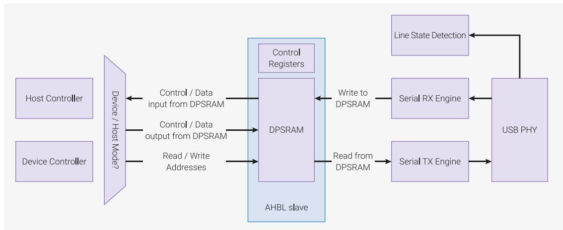
The USB controller is an area-efficient design that muxes a device controller or host controller onto a common set of components. Each component is detailed below.
12.7.3.3. USB PHY
The USB PHY provides the electrical interface between the USB DP and DM pins and the digital logic of the controller. The DP and DM pins are a differential pair, meaning the values are always the inverse of each other, except to encode a specific line state (e.g. SE0 ). The USB PHY drives the DP and DM pins to transmit data and performs a differential receive of any incoming data. The USB PHY provides both single-ended and differential receive data to the line state detection module.
The USB PHY has built in pull-up and pull-down resistors. When the controller acts as a Full Speed device, the DP pin is pulled up to indicate to the host that a Full Speed device has been connected. In host mode, a weak pull-down is applied to DP and DM so that the lines are pulled to a logical zero until the device pulls up DP for Full Speed or DM for Low Speed.
12.7.3.4. Line state detection
The USB 2.0 Specification defines several line states (Bus Reset, Connected, Suspend, Resume, Data 1, Data 0, etc.) that need to be detected. The line state detection module has several state machines to detect these states and signal events to the other hardware components. There is no shared clock signal in USB, so the RX data must be sampled by an internal clock. The maximum data rate of USB Full Speed is 12 Mb/s. The RX data is sampled at 48MHz, giving 4 clock cycles to capture and filter the bus state. The line state detection module distributes the filtered RX data to the Serial RX Engine.
12.7.3.5. Serial RX engine
The serial receive (RX) engine decodes receive data captured by the line state detection module. It produces the following information:
- • The PID of the incoming data packet
- • The device address for the incoming data
- • The device endpoint for the incoming data
- • Data bytes
The serial receive engine also detects errors in RX data by performing a CRC check on the incoming data. Any errors are signalled to the other hardware blocks and can raise an interrupt.
NOTEIf you disconnect the USB cable during packet transfer in either host or device mode, the hardware will raise errors. Software must account for this scenario if you enable error interrupts.
12.7.3.6. Serial TX engineThe serial transmit (TX) engine is a mirror of the serial receive engine. It is connected to the currently active controller (either device or host). It creates TOKEN and DATA packets, calculates the CRC, and transmits them on the bus.
12.7.3.7. DPSRAMThe USB controller uses 4 kB (4096 bytes) of Dual Port SRAM (DPSRAM) to store control registers and data buffers. The DPSRAM is accessible as a 32-bit wide memory at address 0 of the USB controller ( 0x50100000 ).
The DPSRAM has the following characteristics, which differ from most registers on RP2350:
- • Supports 8-bit, 16-bit, and 32-bit accesses (typically, RP2350 registers only support 32-bit accesses)
- • Does not support set/clear aliases. (typically, RP2350 registers support these)
Data Buffers are typically 64 bytes long, as this is the maximum normal packet size for most Full Speed packets. Isochronous endpoints support a maximum buffer size of 1023 bytes. For other packet types, the maximum size is 64 bytes per buffer.
12.7.3.7.1. Concurrent accessThe DPSRAM in the USB controller is asynchronous. The dual port part of the name indicates that both the processor and the USB controller have ports to read and write, and these two ports are in different clock domains. As a result, the processor and USB controller can access the same memory address at the same time. One could write and one could read simultaneously. This could result in inconsistent data reads. You can avoid this scenario by following the rules outlined in this section.
The AVAILABLE bit in the buffer control register indicates who has ownership of a buffer. Set this bit to 1 from the processor to give the controller ownership of the buffer. When it has finished using the buffer, the controller sets the bit back to 0. Set the AVAILABLE bit separately from the rest of the data in the buffer control register so that the rest of the data in the buffer control register is accurate when the AVAILABLE bit is set.
This is necessary because the processor clock clk_sys can run several times faster than the clk_usb clock. Therefore clk_sys can update the data during a USB controller read on a slower clock. The correct process is:
- 1. Write buffer information (length, etc.) to the buffer control register.
- 2. nop for some clk_sys cycles to ensure that at least one clk_usb cycle passes. Consider a scenario where clk_sys runs at 125MHz and clk_usb runs at 48MHz. Because \( \lceil \frac{125}{48} \rceil = 3 \) , you should issue 3 nop instructions between the writes to guarantee that at least one clk_usb cycle has passed.
- 3. Set the AVAILABLE bit.
If clk_sys and clk_usb run at the same frequency, then it is not necessary to set the AVAILABLE bit separately.
NOTEWhen the USB controller writes the status back to the DPSRAM, it does a 16-bit write to the lower 2 bytes for buffer 0 and the upper 2 bytes for buffer 1. When using double-buffered mode, always treat the buffer control register as two 16-bit registers when updating it in software.
12.7.3.7.2. LayoutAddresses
0x0
→
0xff
are used for control registers containing configuration data. The remaining space, addresses
0x100
→
0xffff
(3840 bytes) can be used for data buffers. The controller has control registers that start at address
0x10000
.
The memory layout depends on the USB controller mode:
- • In Device mode, the host can access multiple endpoints, so each endpoint must have endpoint control and buffer control registers.
- • In Host mode, the host software running on the processor decides which endpoints and devices to access. This only requires one set of endpoint control and buffer control registers. As well as software-driven transfers, the host controller can poll up to 15 interrupt endpoints and has a register for each of these interrupt endpoints.
Table 1192. DPSRAM layout
| Offset | Device Function | Host Function |
|---|---|---|
0x0 | Setup packet (8 bytes) | |
0x8 | EP1 in control | Interrupt endpoint control 1 |
0xc | EP1 out control | Spare |
0x10 | EP2 in control | Interrupt endpoint control 2 |
0x14 | EP2 out control | Spare |
0x18 | EP3 in control | Interrupt endpoint control 3 |
0x1c | EP3 out control | Spare |
0x20 | EP4 in control | Interrupt endpoint control 4 |
0x24 | EP4 out control | Spare |
0x28 | EP5 in control | Interrupt endpoint control 5 |
0x2c | EP5 out control | Spare |
0x30 | EP6 in control | Interrupt endpoint control 6 |
0x34 | EP6 out control | Spare |
0x38 | EP7 in control | Interrupt endpoint control 7 |
0x3c | EP7 out control | Spare |
0x40 | EP8 in control | Interrupt endpoint control 8 |
0x44 | EP8 out control | Spare |
0x48 | EP9 in control | Interrupt endpoint control 9 |
0x4c | EP9 out control | Spare |
0x50 | EP10 in control | Interrupt endpoint control 10 |
0x54 | EP10 out control | Spare |
0x58 | EP11 in control | Interrupt endpoint control 11 |
| Offset | Device Function | Host Function |
|---|---|---|
| 0x5c | EP11 out control | Spare |
| 0x60 | EP12 in control | Interrupt endpoint control 12 |
| 0x64 | EP12 out control | Spare |
| 0x68 | EP13 in control | Interrupt endpoint control 13 |
| 0x6c | EP13 out control | Spare |
| 0x70 | EP14 in control | Interrupt endpoint control 14 |
| 0x74 | EP14 out control | Spare |
| 0x78 | EP15 in control | Interrupt endpoint control 15 |
| 0x7c | EP15 out control | Spare |
| 0x80 | EP0 in buffer control | EPx buffer control |
| 0x84 | EP0 out buffer control | Spare |
| 0x88 | EP1 in buffer control | Interrupt endpoint buffer control 1 |
| 0x8c | EP1 out buffer control | Spare |
| 0x90 | EP2 in buffer control | Interrupt endpoint buffer control 2 |
| 0x94 | EP2 out buffer control | Spare |
| 0x98 | EP3 in buffer control | Interrupt endpoint buffer control 3 |
| 0x9c | EP3 out buffer control | Spare |
| 0xa0 | EP4 in buffer control | Interrupt endpoint buffer control 4 |
| 0xa4 | EP4 out buffer control | Spare |
| 0xa8 | EP5 in buffer control | Interrupt endpoint buffer control 5 |
| 0xac | EP5 out buffer control | Spare |
| 0xb0 | EP6 in buffer control | Interrupt endpoint buffer control 6 |
| 0xb4 | EP6 out buffer control | Spare |
| 0xb8 | EP7 in buffer control | Interrupt endpoint buffer control 7 |
| 0xbc | EP7 out buffer control | Spare |
| 0xc0 | EP8 in buffer control | Interrupt endpoint buffer control 8 |
| 0xc4 | EP8 out buffer control | Spare |
| 0xc8 | EP9 in buffer control | Interrupt endpoint buffer control 9 |
| 0xcc | EP9 out buffer control | Spare |
| 0xd0 | EP10 in buffer control | Interrupt endpoint buffer control 10 |
| 0xd4 | EP10 out buffer control | Spare |
| 0xd8 | EP11 in buffer control | Interrupt endpoint buffer control 11 |
| 0xdc | EP11 out buffer control | Spare |
| 0xe0 | EP12 in buffer control | Interrupt endpoint buffer control 12 |
| 0xe4 | EP12 out buffer control | Spare |
| 0xe8 | EP13 in buffer control | Interrupt endpoint buffer control 13 |
| Offset | Device Function | Host Function | Column 3 |
|---|---|---|---|
| 0xec | EP13 | out buffer control | Spare |
| 0xf0 | EP14 | in buffer control | Interrupt endpoint buffer control 14 |
| 0xf4 | EP14 | out buffer control | Spare |
| 0xf8 | EP15 | in buffer control | Interrupt endpoint buffer control 15 |
| 0xfc | EP15 | out buffer control | Spare |
| 0x100 | EP0 | buffer 0 (shared between in and out) | EPx control |
| 0x140 | Optional EP0 | buffer 1 | Spare |
| 0x180 0x180 | Data buffers | ||
| • A device must support Endpoint 0 so that it can reply to | SETUP | packets and be enumerated. As a result, there is no | |
| endpoint control register for | EP0 . Its buffers begin at | 0x100 . All other endpoints can have either single or dual buffers and | |
| are mapped at the base address programmed. As | EP0 has no endpoint control register, the interrupt enable controls for | ||
| EP0 come from SIE_CTRL. Table 1193. Endpoint | |||
| Bit(s) control register layout | Device Function | Host Function | |
| 31 | Endpoint enable Endpoint enable | ||
| 30 | Single buffered (64 bytes) = 0, Double buffered (64 bytes | × 2) = 1 | |
| 29 | Enable interrupt for every transferred buffer | ||
| 28 | Enable interrupt for every 2 transferred buffers (valid for double-buffered only) | ||
| 27:26 27:26 | Endpoint Type: Control = 0, Isochronous = 1, Bulk = 2, Interrupt = 3 | ||
| 25:18 | N/A | The interval the host controller should poll this endpoint. Only applicable for interrupt | |
| 17 | Interrupt on STALL | ||
| 16 | Interrupt on NAK | value of 9 would poll the endpoint every 10ms. | |
| 15:6 15:6 | Address base offset in DPSRAM of data buffer(s) |
12.7.3.7.3. Endpoint control register
The endpoint control register is used to configure an endpoint. It defines:
- • The endpoint type
- • The base address of the endpoint’s data buffer (or data buffers if double-buffered)
- • Which endpoint events trigger the controller interrupt output
A device must support Endpoint 0 so that it can reply to SETUP packets and be enumerated. As a result, there is no endpoint control register for EP0 . Its buffers begin at 0x100 . All other endpoints can have either single or dual buffers and are mapped at the base address programmed. As EP0 has no endpoint control register, the interrupt enable controls for EP0 come from SIE_CTRL .
Table 1193. Endpoint control register layout
NOTE
The data buffer base address must be 64-byte aligned, since bits 0 through 5 are ignored.
12.7.3.7.4. Buffer control register
The buffer control register contains information about the state of the data buffers for that endpoint. It is shared between the processor and the controller. If the endpoint is configured to be single-buffered, only the first half (bits 0 through 15) of the buffer are used.
If double buffering, the buffer select starts at buffer 0. From then on, the buffer select flips between buffer 0 and 1
unless the reset buffer select bit is set (which resets the buffer select to buffer 0). The value of the buffer select is internal to the controller and not accessible by the processor.
For host interrupt and isochronous packets on EPx , the buffer full bit will be set on completion even if the transfer was unsuccessful. To determine the error, read the error bits in the SIE_STATUS register.
Table 1194. Buffer control register layout
| Bit(s) | Function |
|---|---|
| 31 | Buffer 1 full. Should be set to 1 by the processor for an IN transaction and 0 for an OUT transaction. The controller sets this to 1 for an OUT transaction because it has filled the buffer. The controller sets it to 0 for an IN transaction because it has emptied the buffer. Only valid when double buffering. |
| 30 | Last buffer of transfer for buffer 1. Only valid when double buffering. |
| 29 | Data PID for buffer 1 - DATA0 = 0, DATA1 = 1. Only valid when double buffering. |
| 27:28 | Double buffer offset for isochronous mode (0 = 128, 1 = 256, 2 = 512, 3 = 1024). |
| 26 | Buffer 1 available. Whether the buffer can be used by the controller for a transfer. The processor sets this to 1 when the buffer is configured. The controller sets this to 0 after it has sent the data to the host for an IN transaction, or filled the buffer with data from the host for an OUT transaction. Only valid when double buffering. |
| 25:16 | Buffer 1 transfer length. Only valid when double buffering. |
| 15 | Buffer 0 full. Should be set to 1 by the processor for an IN transaction and 0 for an OUT transaction. The controller sets this to 1 for an OUT transaction because it has filled the buffer. The controller sets it to 0 for an IN transaction because it has emptied the buffer. |
| 14 | Last buffer of transfer for buffer 0. |
| 13 | Data PID for buffer 0 - DATA0 = 0, DATA1 = 1. |
| 12 | Reset buffer select to buffer 0 - cleared at end of transfer. For device only . |
| 11 | Send STALL for device, STALL received for host. |
| 10 | Buffer 0 available. Indicates whether the buffer can be used by the controller for a transfer. The processor sets this to 1 when the buffer is configured. The controller sets this to 0 after it has sent the data to the host for an IN transaction or filled the buffer with data from the host for an OUT transaction. |
| 9:0 | Buffer 0 transfer length. |
 WARNING
If you run clk_sys and clk_usb at different speeds, set the available and stall bits after the other data in the buffer control register. Otherwise, the controller may initiate a transaction with data from a previous packet. The controller could see the available bit set, but get the data PID or length from the previous packet.
12.7.3.8. Device controller
This section details how the device controller operates when it receives various packet types from the host.
12.7.3.8.1. SETUP
The device controller MUST always accept a SETUP packet from the host. DPSRAM dedicates its first 8 bytes to the setup packet.
The USB 2.0 Specification states that receiving a setup packet also clears any stall bits on EP0 . For this reason, the stall
bits for EP0 are gated with two bits in the EP_STALL_ARM register. These bits are cleared when a setup packet is received. This means that to send a stall on EP0 , you must set both the stall bit in the buffer control register and the appropriate bit in EP_STALL_ARM .
Barring any errors, the setup packet will be put into the setup packet buffer at DPSRAM offset 0x0 . The device controller will then reply with an ACK .
Finally, SIE_STATUS.SETUP_REC is set to indicate that a setup packet has been received. This will trigger an interrupt if the programmer has enabled the SETUP_REC interrupt (see INTE ).
12.7.3.8.2. IN
From the device's point of view, an IN transfer means transferring data into the host. When an IN token is received from the host, the request is handled as follows:
TOKEN phase:
- 1. If STALL is set in the buffer control register (and if EP0 , the appropriate EP_STALL_ARM bit is set), send a STALL response and go to idle.
- 2. If AVAILABLE and FULL bits are set in buffer control, go to the DATA phase.
- 3. If this is an isochronous endpoint, go to idle.
- ◦ Otherwise, send NAK and go to the DATA phase.
DATA phase:
- 1. Send data.
- 2. If this is an isochronous endpoint, go to idle.
- ◦ Otherwise, go to the ACK phase.
ACK phase:
- 1. Wait for ACK packet from host.
- 2. If there is a timeout, raise a timeout error.
- 3. If ACK is received, the packet is done, so go to STATUS phase.
STATUS phase:
- 1. If this was the last buffer in the transfer (i.e. if the LAST_BUFFER bit in the buffer control register was set), set SIE_STATUS.TRANS_COMPLETE .
- 2. If the endpoint is double buffered, flip the buffer select to the other buffer.
- 3. Set a bit in BUFF_STATUS to indicate the buffer is done. When handling this event, the programmer should read BUFF_CPU_SHOULD_HANDLE to see if it is buffer 0 or buffer 1 that is finished. If the endpoint is double-buffered, both buffers could be done. The cleared BUFF_STATUS bit will be set again, and BUFF_CPU_SHOULD_HANDLE will change in this instance.
- 4. Update status in the appropriate half of the buffer control register: length , pid , and last_buff are set. Everything else is written to zero.
If the host receives a NAK , the host will retry again later.
12.7.3.8.3. OUT
When an OUT token is received from the host, the request is handled as follows:
TOKEN phase:
- 1. If this is not an Isochronous endpoint and the data PID does not match the buffer control register, raise
SIE_STATUS.DATA_SEQ_ERROR (isochronous data is always sent with a DATA0 pid).
- 2. If the AVAILABLE bit is set and the FULL bit is clear, go to the DATA phase, unless the STALL bit is set in which case the device controller will reply with a STALL .
DATA phase:
- 1. Store received data in buffer. If this is an isochronous endpoint, go to the STATUS phase. Otherwise, go to the ACK phase.
ACK phase:
STATUS phase:
See IN STATUS phase: [usb-device-in-status-phase] . There is one difference: the FULL bit is set in the buffer control register to indicate that data has been received. In the IN phase, the FULL bit is cleared to indicate that data has been sent.
12.7.3.8.4. Suspend and resume
The USB device controller supports suspend, resume, and device-initiated remote resume (triggered with SIE_CTRL.RESUME ). There is an interrupt / status bit in SIE_STATUS . It is not necessary to enable the suspend and resume interrupts, since suspend and resume are irrelevant to most devices.
The device goes into suspend when it does not see any start of frame packets (transmitted every 1ms) from the host.
i NOTE
If you enable the suspend interrupt, it is likely you will see a suspend interrupt when the device first connects, but the bus is idle. The bus can be idle for a few milliseconds before the host begins sending start of frame packets. If you do not have a VBUS detect circuit connected, you will also see a suspend interrupt when the device disconnects. Without VBUS detection, it is impossible to tell the difference between being disconnected and suspended.
12.7.3.9. Host controller
The host controller design is similar to the device controller. The host starts all transactions, so the host always deals with transactions it has started. For this reason, there is only one set of endpoint control and endpoint buffer control registers. The host controller also contains additional hardware to poll interrupt endpoints in the background when there are no software controlled transactions taking place.
The host needs to send keep-alive packets to the device every 1ms to keep the device from suspending. Full Speed mode uses a SOF (start of frame) packet. Low Speed mode uses an EOP (end of packet) instead. Set SIE_CTRL.KEEP_ALIVE_EN and SIE_CTRL.SOF_EN to enable these packets.
Several bits in SIE_CTRL are used to begin a host transaction:
- • SEND_SETUP - Send a setup packet. Typically used with RECEIVE_TRANS , so the setup packet will be sent followed by the additional data transaction expected from the device.
- • SEND_TRANS - This transfer is OUT from the host.
- • RECEIVE_TRANS - This transfer is IN to the host.
- • START_TRANS - Start the transfer (non-latching).
- • STOP_TRANS - Stop the current transfer (non-latching).
- • PREAMBLE_ENABLE - Used to send a packet to a Low Speed device on a Full Speed hub. Sends a PRE token packet before every packet the host sends (i.e. PRE , TOKEN , PRE , DATA , pre , ACK ).
- • SOF_SYNC - Used to delay the transaction until after the next SOF . Useful for interrupt and isochronous endpoints. The host controller prevents a transaction of 64 bytes from clashing with the SOF packets. For longer isochronous
packets, software is responsible for preventing collisions. To prevent collisions in software, use
SOF_SYNC
and limit the number of packets sent in one frame. If a transaction is set up with multiple packets,
SOF_SYNC
only applies to the first packet.
The
START_TRANS
bit is synchronised separately from other control bits in the
SIE_CTRL
register because the processor clock
clk_sys
can be asynchronous to the
clk_usb
clock. Always set the
START_TRANS
bit separately from the rest of the data in the
SIE_CTRL
register. Always ensure that at least two
clk_usb
cycles pass between writing to
START_TRANS
and other bits in
SIE_CTRL
. This ensures that the register contents are stable when the controller is prompted to start a transfer.
Consider a scenario where
clk_sys
runs at 125MHz and
clk_usb
runs at 48MHz. Because
\(
\lceil \frac{125}{48} \rceil \times 2 = 6
\)
, you should issue 6
nop
instructions between the writes to guarantee that at least two
clk_usb
cycles have passed.
12.7.3.9.1. SETUP
The
SETUP
packet sent from the host always comes from the dedicated 8 bytes of space at offset
0x0
of the DPSRAM. Like the device controller, there are no control registers associated with the setup packet. The parameters are hard-coded and loaded into the hardware when you write to
START_TRANS
with the
SEND_SETUP
bit set. Once the setup packet has been sent, the host state machine waits for an
ACK
from the device. If there is a timeout, an
RX_TIMEOUT
error will be raised. If the
SEND_TRANS
bit is set, the host state machine will move to the
OUT
phase. Typically, the
SEND_SETUP
packet is used with the
RECEIVE_TRANS
bit, so the controller moves to the
IN
phase after sending a setup packet.
12.7.3.9.2. IN
An
IN
transfer is triggered with the
RECEIVE_TRANS
bit set when the
START_TRANS
bit is set. If the
SEND_SETUP
bit was set, this may be preceded by a
SETUP
packet.
CONTROL phase:
- 1. Read the
EPxcontrol register located at0x80to get the following endpoint information:- ◦ Is it double buffered?
- ◦ What interrupts are enabled?
- ◦ Base address of the data buffer (data buffers if in double-buffered mode)
- ◦ What is the endpoint type?
- 2. Read the
EPxbuffer control register at0x100to get endpoint buffer information, such as transfer length and data PID. - 3. Set the
AVAILABLEbit (the host state machine checks for it). - 4. Clear the
FULLbit.
TOKEN phase:
- 1. Send the
INtoken packet to the device. The target device address and endpoint come from theADDR_ENDPregister.
DATA phase:
- 1. Receive the first data packet from the device.
- 2. Raise RX timeout error if the device doesn't reply.
- 3. If this is
not
an Isochronous endpoint and the data PID does not match the buffer control register, raise
SIE_STATUS.DATA_SEQ_ERROR(isochronous data is always sent with aDATA0pid).
ACK phase:
- 1. Send
ACKto device.
STATUS phase:
- 1. Set the BUFF_STATUS bit and update the buffer control register.
- 2. Set FULL , DATA_PID , WR_LEN , and LAST_BUFF if applicable.
- 3. If this is the last buffer in the transfer, set TRANS_COMPLETE .
CONTROL phase (continued):
The host state machine performs IN transactions until LAST_BUFF is seen in the buffer_control register.
If the host is in double buffered mode, the host controller toggles between the BUF0 and BUF1 sections of the buffer control register.
Otherwise, the controller reads the buffer control register for buffer 0, then waits for FULL to be clear and AVAILABLE to be set before starting the next IN transaction, waiting in the CONTROL phase.
If the host receives a zero length packet, the device has no more data. The host state machine stops listening for more data regardless of if the LAST_BUFF flag was set or not. To detect this from host software, check BUFF_DONE for a data length of 0 in the buffer control register.
12.7.3.9.3. OUT
An OUT transfer is triggered with the SEND_TRANS bit set when the START_TRANS bit is set. This may be preceded by a SETUP packet if the SEND_SETUP bit was set.
CONTROL phase:
- 1. Read the EPx control register to get endpoint information (same as Section 12.7.3.9.2 ).
- 2. Read the EPx buffer control register to get the transfer length and data PID. AVAILABLE and FULL must be set before the transfer can start.
TOKEN phase
- 1. Send an OUT packet to the device. The target device address and endpoint come from the ADDR_ENDP register.
DATA phase:
- 1. Send the first data packet to the device. If the endpoint type is isochronous, there is no
ACK
phase, so the host controller goes straight to status phase. If
ACK
is received, go to status phase. Otherwise:
- ◦ If the host receives no reply, raise SIE_STATUS.RX_TIMEOUT .
- ◦ If the host receives NAK , raise SIE_STATUS.NAK_REC and send the data packet again.
- ◦ If the host receives STALL , raise SIE_STATUS.STALL_REC and go to idle.
STATUS phase:
- 1. Set the BUFF_STATUS bit and update the buffer control register. FULL will be set to 0. TRANS_COMPLETE will be set if this is the last buffer in the transfer.
CONTROL phase (continued):
- 1. If this isn't the last buffer in the transfer, wait for FULL and AVAILABLE to be set in the EPx buffer control register again.
12.7.3.9.4. Interrupt endpoints
The host controller can poll interrupt endpoints on a maximum of 15 endpoints. To enable interrupt endpoints, the programmer must:
- • Pick the next free interrupt endpoint slot on the host controller (starting at 1, to a maximum of 15).
- • Program the appropriate endpoint control register and buffer control register like you would with a normal IN or OUT transfer. Because interrupt endpoints are single-buffered, the BUF1 part of the buffer control register is invalid.
- • Set the address and endpoint of the device in the appropriate ADDR_ENDP register ( ADDR_ENDP1 to ADDR_ENDP15 ).
If the device is Low Speed but attached to a Full Speed hub, the preamble bit should be set. The endpoint direction bit should also be set.
- • Set the corresponding interrupt endpoint active bit (one of bits 1 through 15) in INT_EP_CTRL .
Typically, interrupt endpoints use an IN transfer. The host might poll a USB hub to see if the state of any of its ports have changed. If there is no change, the hub replies with a NAK to the controller, and nothing happens. Similarly, a mouse replies with a NAK unless the mouse has been moved since the last time the interrupt endpoint was polled.
Interrupt endpoints are polled by the controller once a SOF packet has been sent by the host controller.
The controller loops from 1 to 15 and attempts to poll any interrupt endpoint with the EP_ACTIVE bit set to 1 in INT_EP_CTRL . The controller will then read the endpoint control register and the buffer control register to see if there is an available buffer (i.e. FULL + AVAILABLE if an OUT transfer and NOT FULL + AVAILABLE for an IN transfer). If not, the controller will move onto the next interrupt endpoint slot.
If there is an available buffer, the transfer is dealt with the same as a normal IN or OUT transfer and the BUFF_DONE flag in BUFF_STATUS will be set when the interrupt endpoint has a valid buffer.
12.7.3.10. VBUS control
The USB controller can be connected to GPIO pins (see Chapter 9 ) for the following VBUS controls:
- • VBUS enable , used to enable VBUS in host mode. Set in SIE_CTRL .
- • VBUS detect , used to detect that VBUS is present in device mode. Set via a bit in SIE_STATUS . Can also raise a VBUS_DETECT interrupt enabled in INTE .
- • VBUS overcurrent , used to detect an overcurrent event. Applicable to both device and host. VBUS overcurrent is a bit in SIE_STATUS .
It is not necessary to connect up any of these pins to GPIO. The host can permanently supply VBUS and detect a device being connected when either the DP or DM pin is pulled high. VBUS detect can be forced in USB_PWR .
12.7.4. Programmer's model
12.7.4.1. TinyUSB
The RP2350 TinyUSB port is the reference implementation for this USB controller. This port can be found in the following files of the pico-sdk GitHub repository:
dcd_rp2040.c
hcd_rp2040.c
rp2040_usb.h
12.7.4.2. Standalone device example
A standalone USB device example, dev_lowlevel , makes it easier to understand how to interact with the USB controller without needing to understand the TinyUSB abstractions. In addition to endpoint 0, the standalone device has two bulk endpoints: EP1 OUT and EP2 IN . The device is designed to send whatever data it receives on EP1 to EP2 . The example comes with a small Python script that writes "Hello World" into EP1 and checks that it is correctly received on EP2 .
The code included in this section explains setting up the USB device controller to receive. It also shows how software responds to a setup packet received from the host.
Figure 125. USB analyser trace of the dev_lowlevel USB device example. The control transfers are the device enumeration. The first bulk OUT (out from the host) transfer, highlighted in blue, is the host sending "Hello World" to the device. The second bulk transfer IN (in to the host), is the device returning "Hello World" to the host.
| Ch0 | Packet 522 | H ↓ | Reset 15.006 ms |
|---|---|---|---|
| Transfer 0 | F S | Control GET | ADDR 0 |
| ENDP 0 | |||
| bRequest GET_DESCRIPTOR | wValue DEVICE type | ||
| wIndex 0x0000 | Descriptors DEVICE Descriptor | ||
| Ch0 | Packet 646 | H ↓ | Reset 15.006 ms |
| Transfer 1 | F S | Control SET | ADDR 0 |
| ENDP 0 | |||
| bRequest SET_ADDRESS | wValue New address 7 | ||
| wIndex 0x0000 | wLength 0 | ||
| Transfer 2 | F S | Control GET | ADDR 7 |
| ENDP 0 | |||
| bRequest GET_DESCRIPTOR | wValue DEVICE type | ||
| wIndex 0x0000 | Descriptors DEVICE Descriptor | ||
| Transfer 3 | F S | Control GET | ADDR 7 |
| ENDP 0 | |||
| bRequest GET_DESCRIPTOR | wValue CONFIGURATION type, Index 0 | ||
| wIndex 0x0000 | Descriptors CONFIGURATION Descriptor | ||
| Transfer 4 | F S | Control GET | ADDR 7 |
| ENDP 0 | |||
| bRequest GET_DESCRIPTOR | wValue CONFIGURATION type, Index 0 | ||
| wIndex 0x0000 | Descriptors 4 Descriptors | ||
| Transfer 5 | F S | Control GET | ADDR 7 |
| ENDP 0 | |||
| bRequest GET_DESCRIPTOR | wValue STRING type, LANGID codes requested | ||
| wIndex Language ID 0x0000 | Descriptors Lang Supported | ||
| Transfer 6 | F S | Control GET | ADDR 7 |
| ENDP 0 | |||
| bRequest GET_DESCRIPTOR | wValue STRING type, Index 2 | ||
| wIndex Language ID 0x0409 | Descriptors Pico Test Device | ||
| Transfer 7 | F S | Control GET | ADDR 7 |
| ENDP 0 | |||
| bRequest GET_DESCRIPTOR | wValue STRING type, Index 1 | ||
| wIndex Language ID 0x0409 | Descriptors Raspberry Pi | ||
| Transfer 8 | F S | Control SET | ADDR 7 |
| ENDP 0 | |||
| bRequest SET_CONFIGURATION | wValue New Configuration 1 | ||
| wIndex 0x0000 | wLength 0 | ||
| Transfer 9 | F S | Bulk OUT | ADDR 7 |
| ENDP 1 | Bytes Transferred 12 | ||
| Transfer 10 | F S | Bulk IN | ADDR 7 |
| ENDP 2 | Bytes Transferred 12 |
12.7.4.2.1. Device controller initialisation
The following code initialises the USB device:
Pico Examples: https://github.com/raspberrypi/pico-examples/blob/master/usb/device/dev_lowlevel/dev_lowlevel.c Lines 183 - 217
183 void usb_device_init() {
184     // Reset usb controller
185     reset_unreset_block_num_wait_blocking(RESET_USBCTRL);
186
187     // Clear any previous state in dpram just in case
188     memset(usb_dpram, 0, sizeof(*usb_dpram)); ①
189
190     // Enable USB interrupt at processor
191     irq_set_enabled(USBCTRL_IRQ, true);
192
193     // Mux the controller to the onboard usb phy
194     usb_hw->muxing = USB_USB_MUXING_TO_PHY_BITS | USB_USB_MUXING_SOFTCON_BITS;
195
196     // Force VBUS detect so the device thinks it is plugged into a host
197     usb_hw->pwr = USB_USB_PWR_VBUS_DETECT_BITS | USB_USB_PWR_VBUS_DETECT_OVERRIDE_EN_BITS;
198
199     // Enable the USB controller in device mode.
200     usb_hw->main_ctrl = USB_MAIN_CTRL_CONTROLLER_EN_BITS;
201
202     // Enable an interrupt per EP0 transaction
203     usb_hw->sie_ctrl = USB_SIE_CTRL_EP0_INT_1BUF_BITS; ②
204
205     // Enable interrupts for when a buffer is done, when the bus is reset,
206     // and when a setup packet is received
207     usb_hw->inte = USB_INTS_BUFF_STATUS_BITS |
208                   USB_INTS_BUS_RESET_BITS |
209                   USB_INTS_SETUP_REQ_BITS;
210
211     // Set up endpoints (endpoint control registers)
212     // described by device configuration
213     usb_setup_endpoints();
214
215     // Present full speed device by enabling pull up on DP
216     usb_hw_set->sie_ctrl = USB_SIE_CTRL_PULLUP_EN_BITS;
217 }
12.7.4.2.2. Configuring the endpoint control registers for EP1 and EP2
The function
usb_configure_endpoints
loops through each endpoint defined in the device configuration (including EP0 in and EP0 out, which don't have an endpoint control register defined) and calls the
usb_configure_endpoint
function. This sets up the endpoint control register for that endpoint:
Pico Examples: https://github.com/raspberrypi/pico-examples/blob/master/usb/device/dev_lowlevel/dev_lowlevel.c Lines 149 - 164
149 void usb_setup_endpoint(const struct usb_endpoint_configuration *ep) {
150     printf("Set up endpoint 0x%x with buffer address 0x%p\n", ep->descriptor-
        >bEndpointAddress, ep->data_buffer);
151
152     // EP0 doesn't have one so return if that is the case
153     if (!ep->endpoint_control) {
154         return;
155     }
156
157     // Get the data buffer as an offset of the USB controller's DPRAM
158     uint32_t dpram_offset = usb_buffer_offset(ep->data_buffer);
159     uint32_t reg = EP_CTRL_ENABLE_BITS
160                 | EP_CTRL_INTERRUPT_PER_BUFFER
161                 | (ep->descriptor->bmAttributes << EP_CTRL_BUFFER_TYPE_LSB)
162                 | dpram_offset;
163     *ep->endpoint_control = reg;
164 }
12.7.4.2.3. Receiving a setup packet
An interrupt is raised when a setup packet is received, so the interrupt handler must handle this event:
Pico Examples: https://github.com/raspberrypi/pico-examples/blob/master/usb/device/dev_lowlevel/dev_lowlevel.c Lines 494 - 504
494 void isr_usbctrl(void) {
495     // USB interrupt handler
496     uint32_t status = usb_hw->ints;
497     uint32_t handled = 0;
498
499     // Setup packet received
500     if (status & USB_INTS_SETUP_REQ_BITS) {
501         handled |= USB_INTS_SETUP_REQ_BITS;
502         usb_hw_clear->sie_status = USB_SIE_STATUS_SETUP_REC_BITS;
503         usb_handle_setup_packet();
504     }
The controller writes the
SETUP
packet to the first 8 bytes of the DPSRAM, so the setup packet handler casts that area of memory to
struct usb_setup_packet *
:
Pico Examples: https://github.com/raspberrypi/pico-examples/blob/master/usb/device/dev_lowlevel/dev_lowlevel.c Lines 383 - 427
383 void usb_handle_setup_packet(void) {
384     volatile struct usb_setup_packet *pkt = (volatile struct usb_setup_packet *) &usb_dpram
        ->setup_packet;
385     uint8_t req_direction = pkt->bmRequestType;
386     uint8_t req = pkt->bRequest;
387
388     // Reset PID to 1 for EP0 IN
389     usb_get_endpoint_configuration(EP0_IN_ADDR)->next_pid = 1u;
390
391     if (req_direction == USB_DIR_OUT) {
392         if (req == USB_REQUEST_SET_ADDRESS) {
393             usb_set_device_address(pkt);
394         } else if (req == USB_REQUEST_SET_CONFIGURATION) {
395             usb_set_device_configuration(pkt);
396         } else {
397             usb_acknowledge_out_request();
398             printf("Other OUT request (0x%x)\r\n", pkt->bRequest);
399         }
400     } else if (req_direction == USB_DIR_IN) {
401         if (req == USB_REQUEST_GET_DESCRIPTOR) {
402             uint16_t descriptor_type = pkt->wValue >> 8;
403
404             switch (descriptor_type) {
405                 case USB_DT_DEVICE:
406                     usb_handle_device_descriptor(pkt);
407                     printf("GET DEVICE DESCRIPTOR\r\n");
408                     break;
409
410                 case USB_DT_CONFIG:
411                     usb_handle_config_descriptor(pkt);
412                     printf("GET CONFIG DESCRIPTOR\r\n");
413                     break;
414
415                 case USB_DT_STRING:
416                     usb_handle_string_descriptor(pkt);
417                     printf("GET STRING DESCRIPTOR\r\n");
418                     break;
419
420                 default:
421                     printf("Unhandled GET_DESCRIPTOR type 0x%x\r\n", descriptor_type);
422             }
423         } else {
424             printf("Other IN request (0x%x)\r\n", pkt->bRequest);
425         }
426     }
427 }
12.7.4.2.4. Replying to a setup packet on EP0 IN
The host first requests the device descriptor. The following code handles that setup request:
Pico Examples: https://github.com/raspberrypi/pico-examples/blob/master/usb/device/dev_lowlevel/dev_lowlevel.c Lines 266 - 273
266 void usb_handle_device_descriptor(volatile struct usb_setup_packet *pkt) {
267     const struct usb_device_descriptor *d = dev_config.device_descriptor;
268     // EP0 in
269     struct usb_endpoint_configuration *ep = usb_get_endpoint_configuration(EP0_IN_ADDR);
270     // Always respond with pid 1
271     ep->next_pid = 1;
272     usb_start_transfer(ep, (uint8_t *) d, MIN(sizeof(struct usb_device_descriptor), pkt->wLength));
273 }
The
usb_start_transfer
function copies data to be sent into the appropriate hardware buffer and configures the buffer
control register. Once the buffer control register has been written to, the device controller responds to the host with the data. Before this point, the device replies with a NAK :
Pico Examples: https://github.com/raspberrypi/pico-examples/blob/master/usb/device/dev_lowlevel/dev_lowlevel.c Lines 238 - 260
238 void usb_start_transfer(struct usb_endpoint_configuration *ep, uint8_t *buf, uint16_t len) {
239     // We are asserting that the length is <= 64 bytes for simplicity of the example.
240     // For multi packet transfers see the tinyusb port.
241     assert(len <= 64);
242
243     printf("Start transfer of len %d on ep addr 0x%x\n", len, ep->descriptor-
>bEndpointAddress);
244
245     // Prepare buffer control register value
246     uint32_t val = len | USB_BUF_CTRL_AVAIL;
247
248     if (ep_is_tx(ep)) {
249         // Need to copy the data from the user buffer to the usb memory
250         memcpy((void *) ep->data_buffer, (void *) buf, len);
251         // Mark as full
252         val |= USB_BUF_CTRL_FULL;
253     }
254
255     // Set pid and flip for next transfer
256     val |= ep->next_pid ? USB_BUF_CTRL_DATA1_PID : USB_BUF_CTRL_DATA0_PID;
257     ep->next_pid ^= 1u;
258
259     *ep->buffer_control = val;
260 }
12.7.5. List of registers
The USB registers start at a base address of 0x50110000 (defined as USBCTRL_REGS_BASE in SDK).
Table 1195. List of USB registers
| Offset 0x42fc8 0x42fcc 0x42fd0 0x42fd4 0x42fd8 | Name DEVID DEVTYPE PIDR4 PIDR5 PIDR6 | Info Device Configuration register Device Type Identifier register CoreSight Periperal ID4 CoreSight Periperal ID5 CoreSight Periperal ID6 |
|---|---|---|
| Pico Examples: | https://github.com/raspberrypi/pico-examples/blob/master/usb/device/dev_lowlevel/dev_lowlevel.c Lines 238 - 260 | |
| 241 | assert(len <= 64); | |
| 243 | printf("Start transfer of len %d on ep addr 0x%x\n", len, ep->descriptor- | |
| 246 | uint32_t | // Prepare buffer control register value val = len | USB_BUF_CTRL_AVAIL; |
| 248 | if (ep_is_tx(ep)) { | |
| 250 | memcpy((void | *) ep->data_buffer, (void *) buf, len); |
| 251 | // Mark as full | |
| 252 | // Mark as full val | |= USB_BUF_CTRL_FULL; |
| 253 | } | |
| 255 | } // Set pid and flip for next transfer | |
| 256 | // Set pid and flip for next transfer val | |= ep->next_pid ? USB_BUF_CTRL_DATA1_PID : USB_BUF_CTRL_DATA0_PID; |
| 257 | ep->next_pid ^= 1u; | |
| 259 260 } | *ep->buffer_control | = val; |
| 12.7.5. List of registers The USB registers start at a base address of | 0x50110000 (defined as USBCTRL_REGS_BASE in SDK). | |
| Table 1195. List of Offset | Name | Info |
| USB registers 0x000 | ADDR_ENDP | Device address and endpoint control |
| 0x004 | ADDR_ENDP1 | Interrupt endpoint 1. Only valid for HOST mode. |
| 0x008 | ADDR_ENDP2 | Interrupt endpoint 2. Only valid for HOST mode. |
| 0x00c | ADDR_ENDP3 | Interrupt endpoint 3. Only valid for HOST mode. |
| 0x010 | ADDR_ENDP4 | Interrupt endpoint 4. Only valid for HOST mode. |
| 0x014 | ADDR_ENDP5 | Interrupt endpoint 5. Only valid for HOST mode. |
| 0x018 | ADDR_ENDP6 | Interrupt endpoint 6. Only valid for HOST mode. |
| 0x01c | ADDR_ENDP7 | Interrupt endpoint 7. Only valid for HOST mode. |
| 0x020 | ADDR_ENDP8 | Interrupt endpoint 8. Only valid for HOST mode. |
| 0x024 | ADDR_ENDP9 | Interrupt endpoint 9. Only valid for HOST mode. |
| 0x028 | ADDR_ENDP10 | Interrupt endpoint 10. Only valid for HOST mode. |
| 0x02c | ADDR_ENDP11 | Interrupt endpoint 11. Only valid for HOST mode. |
| 0x030 | ADDR_ENDP12 | Interrupt endpoint 12. Only valid for HOST mode. |
| 0x034 | ADDR_ENDP13 | Interrupt endpoint 13. Only valid for HOST mode. |
| Offset | Name | Info |
|---|---|---|
| 0x038 | ADDR_ENDP14 | Interrupt endpoint 14. Only valid for HOST mode. |
| 0x03c | ADDR_ENDP15 | Interrupt endpoint 15. Only valid for HOST mode. |
| 0x040 | MAIN_CTRL | Main control register |
| 0x044 | SOF_WR | Set the SOF (Start of Frame) frame number in the host controller. The SOF packet is sent every 1ms and the host will increment the frame number by 1 each time. |
| 0x048 | SOF_RD | Read the last SOF (Start of Frame) frame number seen. In device mode the last SOF received from the host. In host mode the last SOF sent by the host. |
| 0x04c | SIE_CTRL | SIE control register |
| 0x050 | SIE_STATUS | SIE status register |
| 0x054 | INT_EP_CTRL | interrupt endpoint control register |
| 0x058 | BUFF_STATUS | Buffer status register. A bit set here indicates that a buffer has completed on the endpoint (if the buffer interrupt is enabled). It is possible for 2 buffers to be completed, so clearing the buffer status bit may instantly re set it on the next clock cycle. |
| 0x05c | BUFF_CPU_SHOULD_HANDLE | Which of the double buffers should be handled. Only valid if using an interrupt per buffer (i.e. not per 2 buffers). Not valid for host interrupt endpoint polling because they are only single buffered. |
| 0x060 | EP_ABORT | Device only: Can be set to ignore the buffer control register for this endpoint in case you would like to revoke a buffer. A NAK will be sent for every access to the endpoint until this bit is cleared. A corresponding bit in EP_ABORT_DONE is set when it is safe to modify the buffer control register. |
| 0x064 | EP_ABORT_DONE | Device only: Used in conjunction with EP_ABORT . Set once an endpoint is idle so the programmer knows it is safe to modify the buffer control register. |
| 0x068 | EP_STALL_ARM | Device: this bit must be set in conjunction with the STALL bit in the buffer control register to send a STALL on EP0. The device controller clears these bits when a SETUP packet is received because the USB spec requires that a STALL condition is cleared when a SETUP packet is received. |
| 0x06c | NAK_POLL | Used by the host controller. Sets the wait time in microseconds before trying again if the device replies with a NAK. |
| 0x070 | EP_STATUS_STALL_NAK | Device: bits are set when the IRQ_ON_NAK or IRQ_ON_STALL bits are set. For EP0 this comes from SIE_CTRL . For all other endpoints it comes from the endpoint control register. |
| 0x074 | USB_MUXING | Where to connect the USB controller. Should be to_phy by default. |
| 0x078 | USB_PWR | Overrides for the power signals in the event that the VBUS signals are not hooked up to GPIO. Set the value of the override and then the override enable to switch over to the override value. |
| Offset | Name | Info |
|---|---|---|
| 0x07c | USBPHY_DIRECT | This register allows for direct control of the USB phy. Use in conjunction with
usbphy_direct_override
register to enable each override bit. |
| 0x080 | USBPHY_DIRECT_OVERRIDE | Override enable for each control in
usbphy_direct |
| 0x084 | USBPHY_TRIM | Used to adjust trim values of USB phy pull down resistors. |
| 0x088 | LINESTATE_TUNING | Used for debug only. |
| 0x08c | INTR | Raw Interrupts |
| 0x090 | INTE | Interrupt Enable |
| 0x094 | INTF | Interrupt Force |
| 0x098 | INTS | Interrupt status after masking & forcing |
| 0x100 | SOF_TIMESTAMP_RAW | Device only. Raw value of free-running PHY clock counter @48MHz. Used to calculate time between SOF events. |
| 0x104 | SOF_TIMESTAMP_LAST | Device only. Value of free-running PHY clock counter @48MHz when last SOF event occurred. |
| 0x108 | SM_STATE | |
| 0x10c | EP_TX_ERROR | TX error count for each endpoint. Write to each field to reset the counter to 0. |
| 0x110 | EP_RX_ERROR | RX error count for each endpoint. Write to each field to reset the counter to 0. |
| 0x114 | DEV_SM_WATCHDOG | Watchdog that forces the device state machine to idle and raises an interrupt if the device stays in a state that isn't idle for the configured limit. The counter is reset on every state transition. Set limit while enable is low and then set the enable. |
USB: ADDR_ENDP Register
Offset: 0x000
Description
Device address and endpoint control
Table 1196.
ADDR_ENDP Register
| Bits | Description | Type | Reset |
|---|---|---|---|
| 31:20 | Reserved. | - | - |
| 19:16 | ENDPOINT: Device endpoint to send data to. Only valid for HOST mode. | RW | 0x0 |
| 15:7 | Reserved. | - | - |
| 6:0 | ADDRESS: In device mode, the address that the device should respond to. Set in response to a SET_ADDR setup packet from the host. In host mode set to the address of the device to communicate with. | RW | 0x00 |
USB: ADDR_ENDP1, ADDR_ENDP2, ..., ADDR_ENDP14, ADDR_ENDP15 Registers
Offsets: 0x004, 0x008, ..., 0x038, 0x03c
Description
Interrupt endpoint N . Only valid for HOST mode.
Table 1197.
ADDR_ENDP1,
ADDR_ENDP2, ...,
ADDR_ENDP14,
ADDR_ENDP15
Registers
| Bits | Description | Type | Reset |
|---|---|---|---|
| 31:27 | Reserved. | - | - |
| 26 | INTEP_PREAMBLE : Interrupt EP requires preamble (is a low speed device on a full speed hub) | RW | 0x0 |
| 25 | INTEP_DIR : Direction of the interrupt endpoint. In=0, Out=1 | RW | 0x0 |
| 24:20 | Reserved. | - | - |
| 19:16 | ENDPOINT : Endpoint number of the interrupt endpoint | RW | 0x0 |
| 15:7 | Reserved. | - | - |
| 6:0 | ADDRESS : Device address | RW | 0x00 |
USB: MAIN_CTRL Register
Offset: 0x040
Description
Main control register
Table 1198.
MAIN_CTRL Register
| Bits | Description | Type | Reset |
|---|---|---|---|
| 31 | SIM_TIMING : Reduced timings for simulation | RW | 0x0 |
| 30:3 | Reserved. | - | - |
| 2 | PHY_ISO
: Isolates USB phy after controller power-up Remove isolation once software has configured the controller Not isolated = 0, Isolated = 1 | RW | 0x1 |
| 1 | HOST_NDEVICE : Device mode = 0, Host mode = 1 | RW | 0x0 |
| 0 | CONTROLLER_EN : Enable controller | RW | 0x0 |
USB: SOF_WR Register
Offset: 0x044
Description
Set the SOF (Start of Frame) frame number in the host controller. The SOF packet is sent every 1ms and the host will increment the frame number by 1 each time.
Table 1199. SOF_WR
Register
| Bits | Description | Type | Reset |
|---|---|---|---|
| 31:11 | Reserved. | - | - |
| 10:0 | COUNT | WF | 0x000 |
USB: SOF_RD Register
Offset: 0x048
Description
Read the last SOF (Start of Frame) frame number seen. In device mode the last SOF received from the host. In host mode the last SOF sent by the host.
Table 1200. SOF_RD Register| Bits | Description | Type | Reset |
|---|---|---|---|
| 31:11 | Reserved. | - | - |
| 10:0 | COUNT | RO | 0x000 |
USB: SIE_CTRL Register
Offset: 0x04c
Description
SIE control register
Table 1201. SIE_CTRL Register| Bits | Description | Type | Reset |
|---|---|---|---|
| 31 | EP0_INT_STALL : Device: Set bit in EP_STATUS_STALL_NAK when EP0 sends a STALL | RW | 0x0 |
| 30 | EP0_DOUBLE_BUF : Device: EP0 single buffered = 0, double buffered = 1 | RW | 0x0 |
| 29 | EP0_INT_1BUF : Device: Set bit in BUFF_STATUS for every buffer completed on EP0 | RW | 0x0 |
| 28 | EP0_INT_2BUF : Device: Set bit in BUFF_STATUS for every 2 buffers completed on EP0 | RW | 0x0 |
| 27 | EP0_INT_NAK : Device: Set bit in EP_STATUS_STALL_NAK when EP0 sends a NAK | RW | 0x0 |
| 26 | DIRECT_EN : Direct bus drive enable | RW | 0x0 |
| 25 | DIRECT_DP : Direct control of DP | RW | 0x0 |
| 24 | DIRECT_DM : Direct control of DM | RW | 0x0 |
| 23:20 | Reserved. | - | - |
| 19 | EP0_STOP_ON_SHORT_PACKET : Device: Stop EP0 on a short packet. | RW | 0x0 |
| 18 | TRANSCEIVER_PD : Power down bus transceiver | RW | 0x0 |
| 17 | RPU_OPT : Device: Pull-up strength (0=1K2, 1=2k3) | RW | 0x0 |
| 16 | PULLUP_EN : Device: Enable pull up resistor | RW | 0x0 |
| 15 | PULLDOWN_EN : Host: Enable pull down resistors | RW | 0x1 |
| 14 | Reserved. | - | - |
| 13 | RESET_BUS : Host: Reset bus | SC | 0x0 |
| 12 | RESUME : Device: Remote wakeup. Device can initiate its own resume after suspend. | SC | 0x0 |
| 11 | VBUS_EN : Host: Enable VBUS | RW | 0x0 |
| 10 | KEEP_ALIVE_EN : Host: Enable keep alive packet (for low speed bus) | RW | 0x0 |
| 9 | SOF_EN : Host: Enable SOF generation (for full speed bus) | RW | 0x0 |
| 8 | SOF_SYNC : Host: Delay packet(s) until after SOF | RW | 0x0 |
| 7 | Reserved. | - | - |
| 6 | PREAMBLE_EN : Host: Preable enable for LS device on FS hub | RW | 0x0 |
| 5 | Reserved. | - | - |
| 4 | STOP_TRANS : Host: Stop transaction | SC | 0x0 |
| Bits | Description | Type | Reset |
|---|---|---|---|
| 3 | RECEIVE_DATA : Host: Receive transaction (IN to host) | RW | 0x0 |
| 2 | SEND_DATA : Host: Send transaction (OUT from host) | RW | 0x0 |
| 1 | SEND_SETUP : Host: Send Setup packet | RW | 0x0 |
| 0 | START_TRANS : Host: Start transaction | SC | 0x0 |
USB: SIE_STATUS Register
Offset: 0x050
Description
SIE status register
Table 1202.
SIE_STATUS Register
| Bits | Description | Type | Reset |
|---|---|---|---|
| 31 | DATA_SEQ_ERROR
: Data Sequence Error. The device can raise a sequence error in the following conditions: * A SETUP packet is received followed by a DATA1 packet (data phase should always be DATA0) * An OUT packet is received from the host but doesn't match the data pid in the buffer control register read from DPSRAM The host can raise a data sequence error in the following conditions: * An IN packet from the device has the wrong data PID | WC | 0x0 |
| 30 | ACK_REC : ACK received. Raised by both host and device. | WC | 0x0 |
| 29 | STALL_REC : Host: STALL received | WC | 0x0 |
| 28 | NAK_REC : Host: NAK received | WC | 0x0 |
| 27 | RX_TIMEOUT : RX timeout is raised by both the host and device if an ACK is not received in the maximum time specified by the USB spec. | WC | 0x0 |
| 26 | RX_OVERFLOW : RX overflow is raised by the Serial RX engine if the incoming data is too fast. | WC | 0x0 |
| 25 | BIT_STUFF_ERROR : Bit Stuff Error. Raised by the Serial RX engine. | WC | 0x0 |
| 24 | CRC_ERROR : CRC Error. Raised by the Serial RX engine. | WC | 0x0 |
| 23 | ENDPOINT_ERROR : An endpoint has encountered an error. Read the ep_rx_error and ep_tx_error registers to find out which endpoint had an error. | WC | 0x0 |
| 22:20 | Reserved. | - | - |
| 19 | BUS_RESET : Device: bus reset received | WC | 0x0 |
| Bits 14:10 9:5 4:0 Bits | Description SHIFT Description | MASK_MSB : The most-significant bit allowed to pass by the mask (inclusive) MASK_LSB : The least-significant bit allowed to pass by the mask (inclusive) : Right-rotate applied to accumulator before masking. By appropriately | Type RW RW RW Type | Reset 0x00 0x00 0x00 Reset |
|---|---|---|---|---|
| 15:13 | Reserved. | - | - | |
| 12 | RX_SHORT_PACKET | : Device or Host has received a short packet. This is when | WC | 0x0 |
| 11 | RESUME | registers. Host: the current transfer will be stopped early. : Host: Device has initiated a remote resume. Device: host has | WC | 0x0 |
| 10 | VBUS_OVER_CURR | initiated a resume. : VBUS over current detected | RO | 0x0 |
| 9:8 | SPEED | : Host: device speed. Disconnected = 00, LS = 01, FS = 10 | RO | 0x0 |
| 7:5 | Reserved. | - | - | |
| 4 | SUSPENDED | : Bus in suspended state. Valid for device and host. Host and | RO | 0x0 |
| 3:2 | LINE_STATE | device will go into suspend if neither Keep Alive / SOF frames are enabled. : USB bus line state | RO | 0x0 |
| 1 | Reserved. | - | - | |
| 0 | VBUS_DETECTED | : Device: VBUS Detected | RO | 0x0 |
| Table 1203. Bits | Description | Type | Reset | |
| INT_EP_CTRL Register 31:16 | Reserved. | - | - | |
| 15:1 | INT_EP_ACTIVE | : Host: Enable interrupt endpoint 1 | → 15 RW | 0x0000 |
| 0 | Reserved. | - | - |
USB: INT_EP_CTRL Register
Offset: 0x054
Description
interrupt endpoint control register
Table 1203.
INT_EP_CTRL Register
USB: BUFF_STATUS Register
Offset: 0x058 DescriptionBuffer status register. A bit set here indicates that a buffer has completed on the endpoint (if the buffer interrupt is enabled). It is possible for 2 buffers to be completed, so clearing the buffer status bit may instantly re set it on the next clock cycle.
Table 1204.
BUFF_STATUS
Register
| Bits | Description | Type | Reset |
|---|---|---|---|
| 31 | EP15_OUT | WC | 0x0 |
| 30 | EP15_IN | WC | 0x0 |
| 29 | EP14_OUT | WC | 0x0 |
| 28 | EP14_IN | WC | 0x0 |
| 27 | EP13_OUT | WC | 0x0 |
| 26 | EP13_IN | WC | 0x0 |
| 25 | EP12_OUT | WC | 0x0 |
| 24 | EP12_IN | WC | 0x0 |
| 23 | EP11_OUT | WC | 0x0 |
| 22 | EP11_IN | WC | 0x0 |
| 21 | EP10_OUT | WC | 0x0 |
| 20 | EP10_IN | WC | 0x0 |
| 19 | EP9_OUT | WC | 0x0 |
| 18 | EP9_IN | WC | 0x0 |
| 17 | EP8_OUT | WC | 0x0 |
| 16 | EP8_IN | WC | 0x0 |
| 15 | EP7_OUT | WC | 0x0 |
| 14 | EP7_IN | WC | 0x0 |
| 13 | EP6_OUT | WC | 0x0 |
| 12 | EP6_IN | WC | 0x0 |
| 11 | EP5_OUT | WC | 0x0 |
| 10 | EP5_IN | WC | 0x0 |
| 9 | EP4_OUT | WC | 0x0 |
| 8 | EP4_IN | WC | 0x0 |
| 7 | EP3_OUT | WC | 0x0 |
| 6 | EP3_IN | WC | 0x0 |
| 5 | EP2_OUT | WC | 0x0 |
| 4 | EP2_IN | WC | 0x0 |
| 3 | EP1_OUT | WC | 0x0 |
| 2 | EP1_IN | WC | 0x0 |
| 1 | EP0_OUT | WC | 0x0 |
| 0 | EP0_IN | WC | 0x0 |
USB: BUFF_CPU_SHOULD_HANDLE Register
Offset: 0x05c
Description
Which of the double buffers should be handled. Only valid if using an interrupt per buffer (i.e. not per 2 buffers). Not valid for host interrupt endpoint polling because they are only single buffered.
Table 1205.
BUFF_CPU_SHOULD_H
ANDLE Register
| Bits | Description | Type | Reset |
|---|---|---|---|
| 31 | EP15_OUT | RO | 0x0 |
| 30 | EP15_IN | RO | 0x0 |
| 29 | EP14_OUT | RO | 0x0 |
| 28 | EP14_IN | RO | 0x0 |
| 27 | EP13_OUT | RO | 0x0 |
| 26 | EP13_IN | RO | 0x0 |
| 25 | EP12_OUT | RO | 0x0 |
| 24 | EP12_IN | RO | 0x0 |
| 23 | EP11_OUT | RO | 0x0 |
| 22 | EP11_IN | RO | 0x0 |
| 21 | EP10_OUT | RO | 0x0 |
| 20 | EP10_IN | RO | 0x0 |
| 19 | EP9_OUT | RO | 0x0 |
| 18 | EP9_IN | RO | 0x0 |
| 17 | EP8_OUT | RO | 0x0 |
| 16 | EP8_IN | RO | 0x0 |
| 15 | EP7_OUT | RO | 0x0 |
| 14 | EP7_IN | RO | 0x0 |
| 13 | EP6_OUT | RO | 0x0 |
| 12 | EP6_IN | RO | 0x0 |
| 11 | EP5_OUT | RO | 0x0 |
| 10 | EP5_IN | RO | 0x0 |
| 9 | EP4_OUT | RO | 0x0 |
| 8 | EP4_IN | RO | 0x0 |
| 7 | EP3_OUT | RO | 0x0 |
| 6 | EP3_IN | RO | 0x0 |
| 5 | EP2_OUT | RO | 0x0 |
| 4 | EP2_IN | RO | 0x0 |
| 3 | EP1_OUT | RO | 0x0 |
| 2 | EP1_IN | RO | 0x0 |
| 1 | EP0_OUT | RO | 0x0 |
| Bits | Description | Type | Reset |
|---|---|---|---|
| 0 | EP0_IN | RO | 0x0 |
USB: EP_ABORT Register
Offset: 0x060
Description
Device only: Can be set to ignore the buffer control register for this endpoint in case you would like to revoke a buffer. A NAK will be sent for every access to the endpoint until this bit is cleared. A corresponding bit in EP_ABORT_DONE is set when it is safe to modify the buffer control register.
Table 1206.
EP_ABORT Register
| Bits | Description | Type | Reset |
|---|---|---|---|
| 31 | EP15_OUT | RW | 0x0 |
| 30 | EP15_IN | RW | 0x0 |
| 29 | EP14_OUT | RW | 0x0 |
| 28 | EP14_IN | RW | 0x0 |
| 27 | EP13_OUT | RW | 0x0 |
| 26 | EP13_IN | RW | 0x0 |
| 25 | EP12_OUT | RW | 0x0 |
| 24 | EP12_IN | RW | 0x0 |
| 23 | EP11_OUT | RW | 0x0 |
| 22 | EP11_IN | RW | 0x0 |
| 21 | EP10_OUT | RW | 0x0 |
| 20 | EP10_IN | RW | 0x0 |
| 19 | EP9_OUT | RW | 0x0 |
| 18 | EP9_IN | RW | 0x0 |
| 17 | EP8_OUT | RW | 0x0 |
| 16 | EP8_IN | RW | 0x0 |
| 15 | EP7_OUT | RW | 0x0 |
| 14 | EP7_IN | RW | 0x0 |
| 13 | EP6_OUT | RW | 0x0 |
| 12 | EP6_IN | RW | 0x0 |
| 11 | EP5_OUT | RW | 0x0 |
| 10 | EP5_IN | RW | 0x0 |
| 9 | EP4_OUT | RW | 0x0 |
| 8 | EP4_IN | RW | 0x0 |
| 7 | EP3_OUT | RW | 0x0 |
| 6 | EP3_IN | RW | 0x0 |
| 5 | EP2_OUT | RW | 0x0 |
| 4 | EP2_IN | RW | 0x0 |
| Bits | Description | Type | Reset |
|---|---|---|---|
| 3 | EP1_OUT | RW | 0x0 |
| 2 | EP1_IN | RW | 0x0 |
| 1 | EP0_OUT | RW | 0x0 |
| 0 | EP0_IN | RW | 0x0 |
USB: EP_ABORT_DONE Register
Offset: 0x064
Description
Device only: Used in conjunction with EP_ABORT . Set once an endpoint is idle so the programmer knows it is safe to modify the buffer control register.
Table 1207.
EP_ABORT_DONE
Register
| Bits | Description | Type | Reset |
|---|---|---|---|
| 31 | EP15_OUT | WC | 0x0 |
| 30 | EP15_IN | WC | 0x0 |
| 29 | EP14_OUT | WC | 0x0 |
| 28 | EP14_IN | WC | 0x0 |
| 27 | EP13_OUT | WC | 0x0 |
| 26 | EP13_IN | WC | 0x0 |
| 25 | EP12_OUT | WC | 0x0 |
| 24 | EP12_IN | WC | 0x0 |
| 23 | EP11_OUT | WC | 0x0 |
| 22 | EP11_IN | WC | 0x0 |
| 21 | EP10_OUT | WC | 0x0 |
| 20 | EP10_IN | WC | 0x0 |
| 19 | EP9_OUT | WC | 0x0 |
| 18 | EP9_IN | WC | 0x0 |
| 17 | EP8_OUT | WC | 0x0 |
| 16 | EP8_IN | WC | 0x0 |
| 15 | EP7_OUT | WC | 0x0 |
| 14 | EP7_IN | WC | 0x0 |
| 13 | EP6_OUT | WC | 0x0 |
| 12 | EP6_IN | WC | 0x0 |
| 11 | EP5_OUT | WC | 0x0 |
| 10 | EP5_IN | WC | 0x0 |
| 9 | EP4_OUT | WC | 0x0 |
| 8 | EP4_IN | WC | 0x0 |
| 7 | EP3_OUT | WC | 0x0 |
| 6 | EP3_IN | WC | 0x0 |
| Bits | Description | Type | Reset |
|---|---|---|---|
| 5 | EP2_OUT | WC | 0x0 |
| 4 | EP2_IN | WC | 0x0 |
| 3 | EP1_OUT | WC | 0x0 |
| 2 | EP1_IN | WC | 0x0 |
| 1 | EP0_OUT | WC | 0x0 |
| 0 | EP0_IN | WC | 0x0 |
USB: EP_STALL_ARM Register
Offset: 0x068
Description
Device: this bit must be set in conjunction with the STALL bit in the buffer control register to send a STALL on EP0. The device controller clears these bits when a SETUP packet is received because the USB spec requires that a STALL condition is cleared when a SETUP packet is received.
Table 1208.
EP_STALL_ARM
Register
| Bits | Description | Type | Reset |
|---|---|---|---|
| 31:2 | Reserved. | - | - |
| 1 | EP0_OUT | RW | 0x0 |
| 0 | EP0_IN | RW | 0x0 |
USB: NAK_POLL Register
Offset: 0x06c
Description
Used by the host controller. Sets the wait time in microseconds before trying again if the device replies with a NAK.
Table 1209.
NAK_POLL Register
| Bits | Description | Type | Reset |
|---|---|---|---|
| 31:28 | RETRY_COUNT_HI: Bits 9:6 of nak_retry count | RO | 0x0 |
| 27 | EPX_STOPPED_ON_NAK: EPX polling has stopped because a nak was received | WC | 0x0 |
| 26 | STOP_EPX_ON_NAK: Stop polling epX when a nak is received | RW | 0x0 |
| 25:16 | DELAY_FS: NAK polling interval for a full speed device | RW | 0x010 |
| 15:10 | RETRY_COUNT_LO: Bits 5:0 of nak_retry_count | RO | 0x00 |
| 9:0 | DELAY_LS: NAK polling interval for a low speed device | RW | 0x010 |
USB: EP_STATUS_STALL_NAK Register
Offset: 0x070
Description
Device: bits are set when the IRQ_ON_NAK or IRQ_ON_STALL bits are set. For EP0 this comes from SIE_CTRL . For all other endpoints it comes from the endpoint control register.
Table 1210.
EP_STATUS_STALL_NAK
Register
| Bits | Description | Type | Reset |
|---|---|---|---|
| 31 | EP15_OUT | WC | 0x0 |
| 30 | EP15_IN | WC | 0x0 |
| Bits | Description | Type | Reset |
|---|---|---|---|
| 29 | EP14_OUT | WC | 0x0 |
| 28 | EP14_IN | WC | 0x0 |
| 27 | EP13_OUT | WC | 0x0 |
| 26 | EP13_IN | WC | 0x0 |
| 25 | EP12_OUT | WC | 0x0 |
| 24 | EP12_IN | WC | 0x0 |
| 23 | EP11_OUT | WC | 0x0 |
| 22 | EP11_IN | WC | 0x0 |
| 21 | EP10_OUT | WC | 0x0 |
| 20 | EP10_IN | WC | 0x0 |
| 19 | EP9_OUT | WC | 0x0 |
| 18 | EP9_IN | WC | 0x0 |
| 17 | EP8_OUT | WC | 0x0 |
| 16 | EP8_IN | WC | 0x0 |
| 15 | EP7_OUT | WC | 0x0 |
| 14 | EP7_IN | WC | 0x0 |
| 13 | EP6_OUT | WC | 0x0 |
| 12 | EP6_IN | WC | 0x0 |
| 11 | EP5_OUT | WC | 0x0 |
| 10 | EP5_IN | WC | 0x0 |
| 9 | EP4_OUT | WC | 0x0 |
| 8 | EP4_IN | WC | 0x0 |
| 7 | EP3_OUT | WC | 0x0 |
| 6 | EP3_IN | WC | 0x0 |
| 5 | EP2_OUT | WC | 0x0 |
| 4 | EP2_IN | WC | 0x0 |
| 3 | EP1_OUT | WC | 0x0 |
| 2 | EP1_IN | WC | 0x0 |
| 1 | EP0_OUT | WC | 0x0 |
| 0 | EP0_IN | WC | 0x0 |
USB: USB_MUXING Register
Offset: 0x074
Description
Where to connect the USB controller. Should be to_phy by default.
Table 1211.
USB_MUXING Register
| Bits | Description | Type | Reset |
|---|---|---|---|
| 31 | SWAP_DPDM : Swap the USB PHY DP and DM pins and all related controls and flip receive differential data. Can be used to switch USB DP/DP on the PCB. This is done at a low level so overrides all other controls. | RW | 0x0 |
| 30:5 | Reserved. | - | - |
| 4 | USBPHY_AS_GPIO : Use the usb DP and DM pins as GPIO pins instead of connecting them to the USB controller. | RW | 0x0 |
| 3 | SOFTCON | RW | 0x0 |
| 2 | TO_DIGITAL_PAD | RW | 0x0 |
| 1 | TO_EXTPHY | RW | 0x0 |
| 0 | TO_PHY | RW | 0x1 |
USB: USB_PWR Register
Offset: 0x078
Description
Overrides for the power signals in the event that the VBUS signals are not hooked up to GPIO. Set the value of the override and then the override enable to switch over to the override value.
Table 1212. USB_PWR Register
| Bits | Description | Type | Reset |
|---|---|---|---|
| 31:6 | Reserved. | - | - |
| 5 | OVERCURR_DETECT_EN | RW | 0x0 |
| 4 | OVERCURR_DETECT | RW | 0x0 |
| 3 | VBUS_DETECT_OVERRIDE_EN | RW | 0x0 |
| 2 | VBUS_DETECT | RW | 0x0 |
| 1 | VBUS_EN_OVERRIDE_EN | RW | 0x0 |
| 0 | VBUS_EN | RW | 0x0 |
USB: USBPHY_DIRECT Register
Offset: 0x07c
Description
This register allows for direct control of the USB phy. Use in conjunction with usbphy_direct_override register to enable each override bit.
Table 1213.
USBPHY_DIRECT Register
| Bits | Description | Type | Reset |
|---|---|---|---|
| 31:26 | Reserved. | - | - |
| 25 | RX_DM_OVERRIDE : Override rx_dm value into controller | RW | 0x0 |
| 24 | RX_DP_OVERRIDE : Override rx_dp value into controller | RW | 0x0 |
| 23 | RX_DD_OVERRIDE : Override rx_dd value into controller | RW | 0x0 |
| 22 | DM_OVV : DM over voltage | RO | 0x0 |
| 21 | DP_OVV : DP over voltage | RO | 0x0 |
| 20 | DM_OVCN : DM overcurrent | RO | 0x0 |
| Bits | Description | Type | Reset |
|---|---|---|---|
| 19 | DP_OVCN : DP overcurrent | RO | 0x0 |
| 18 | RX_DM : DPM pin state | RO | 0x0 |
| 17 | RX_DP : DPP pin state | RO | 0x0 |
| 16 | RX_DD : Differential RX | RO | 0x0 |
| 15 | TX_DIFFMODE
: TX_DIFFMODE=0: Single ended mode TX_DIFFMODE=1: Differential drive mode (TX_DM, TX_DM_OE ignored) | RW | 0x0 |
| 14 | TX_FSSLEW
: TX_FSSLEW=0: Low speed slew rate TX_FSSLEW=1: Full speed slew rate | RW | 0x0 |
| 13 | TX_PD : TX power down override (if override enable is set). 1 = powered down. | RW | 0x0 |
| 12 | RX_PD : RX power down override (if override enable is set). 1 = powered down. | RW | 0x0 |
| 11 | TX_DM
: Output data. TX_DIFFMODE=1, Ignored TX_DIFFMODE=0, Drives DPM only. TX_DM_OE=1 to enable drive. DPM=TX_DM | RW | 0x0 |
| 10 | TX_DP
: Output data. If TX_DIFFMODE=1, Drives DPP/DPM diff pair. TX_DP_OE=1 to enable drive. DPP=TX_DP, DPM=~TX_DP If TX_DIFFMODE=0, Drives DPP only. TX_DP_OE=1 to enable drive. DPP=TX_DP | RW | 0x0 |
| 9 | TX_DM_OE
: Output enable. If TX_DIFFMODE=1, Ignored. If TX_DIFFMODE=0, OE for DPM only. 0 - DPM in Hi-Z state; 1 - DPM driving | RW | 0x0 |
| 8 | TX_DP_OE
: Output enable. If TX_DIFFMODE=1, OE for DPP/DPM diff pair. 0 - DPP/DPM in Hi-Z state; 1 - DPP/DPM driving If TX_DIFFMODE=0, OE for DPP only. 0 - DPP in Hi-Z state; 1 - DPP driving | RW | 0x0 |
| 7 | Reserved. | - | - |
| 6 | DM_PULLDN_EN : DM pull down enable | RW | 0x0 |
| 5 | DM_PULLUP_EN : DM pull up enable | RW | 0x0 |
| 4 | DM_PULLUP_HISEL : Enable the second DM pull up resistor. 0 - Pull = Rpu2; 1 - Pull = Rpu1 + Rpu2 | RW | 0x0 |
| 3 | Reserved. | - | - |
| 2 | DP_PULLDN_EN : DP pull down enable | RW | 0x0 |
| 1 | DP_PULLUP_EN : DP pull up enable | RW | 0x0 |
| 0 | DP_PULLUP_HISEL : Enable the second DP pull up resistor. 0 - Pull = Rpu2; 1 - Pull = Rpu1 + Rpu2 | RW | 0x0 |
USB: USBPHY_DIRECT_OVERRIDE Register
Offset: 0x080
Description
Override enable for each control in usbphy_direct
Table 1214.
USBPHY_DIRECT_OVERRIDE Register
| Bits | Description | Type | Reset |
|---|---|---|---|
| 31:19 | Reserved. | - | - |
| 18 | RX_DM_OVERRIDE_EN | RW | 0x0 |
| Bits | Description | Type | Reset |
|---|---|---|---|
| 17 | RX_DP_OVERRIDE_EN | RW | 0x0 |
| 16 | RX_DD_OVERRIDE_EN | RW | 0x0 |
| 15 | TX_DIFFMODE_OVERRIDE_EN | RW | 0x0 |
| 14:13 | Reserved. | - | - |
| 12 | DM_PULLUP_OVERRIDE_EN | RW | 0x0 |
| 11 | TX_FSSLEW_OVERRIDE_EN | RW | 0x0 |
| 10 | TX_PD_OVERRIDE_EN | RW | 0x0 |
| 9 | RX_PD_OVERRIDE_EN | RW | 0x0 |
| 8 | TX_DM_OVERRIDE_EN | RW | 0x0 |
| 7 | TX_DP_OVERRIDE_EN | RW | 0x0 |
| 6 | TX_DM_OE_OVERRIDE_EN | RW | 0x0 |
| 5 | TX_DP_OE_OVERRIDE_EN | RW | 0x0 |
| 4 | DM_PULLDN_EN_OVERRIDE_EN | RW | 0x0 |
| 3 | DP_PULLDN_EN_OVERRIDE_EN | RW | 0x0 |
| 2 | DP_PULLUP_EN_OVERRIDE_EN | RW | 0x0 |
| 1 | DM_PULLUP_HISEL_OVERRIDE_EN | RW | 0x0 |
| 0 | DP_PULLUP_HISEL_OVERRIDE_EN | RW | 0x0 |
USB: USBPHY_TRIM Register
Offset: 0x084
Description
Used to adjust trim values of USB phy pull down resistors.
Table 1215.
USBPHY_TRIM
Register
| Bits | Description | Type | Reset |
|---|---|---|---|
| 31:13 | Reserved. | - | - |
| 12:8 | DM_PULLDN_TRIM:
Value to drive to USB PHY DM pulldown resistor trim control Experimental data suggests that the reset value will work, but this register allows adjustment if required | RW | 0x1f |
| 7:5 | Reserved. | - | - |
| 4:0 | DP_PULLDN_TRIM:
Value to drive to USB PHY DP pulldown resistor trim control Experimental data suggests that the reset value will work, but this register allows adjustment if required | RW | 0x1f |
USB: LINESTATE_TUNING Register
Offset: 0x088
Description
Used for debug only.
Table 1216.
LINESTATE_TUNING
Register
| Bits 2 1 0 Bits | Description RESET PUSH DATA Description | : Reset (before sending a new key) | Type RW RW RW Type | Reset 0x0 0x0 0x0 Reset |
|---|---|---|---|---|
| Register 31:12 | Reserved. | - | - | |
| 11:8 | SPARE_FIX | RW | 0x0 | |
| 7 | DEV_LS_WAKE_FIX | : Device - exit suspend on any non-idle signalling, not qualified with a 1ms timer | RW | 0x1 |
| 6 | DEV_RX_ERR_QUIESCE | : Device - suppress repeated errors until the device FSM is next in the process of decoding an inbound packet. | RW | 0x1 |
| 5 | SIE_RX_CHATTER_SE0_FIX | : RX - when recovering from line chatter or bitstuff errors, treat SE0 as the end of chatter as well as 8 consecutive idle bits. | RW | 0x1 |
| 4 | SIE_RX_BITSTUFF_FIX | : RX - when a bitstuff error is signalled by rx_dasm, unconditionally terminate RX decode to avoid a hang during certain packet phases. | RW | 0x1 |
| 3 | DEV_BUFF_CONTROL_DOUBLE_READ_FIX match. | : Device - the controller FSM performs two reads of the buffer status memory address to | RW | 0x1 |
| 2 | MULTI_HUB_FIX | : Host - increase inter-packet and turnaround timeouts to accommodate worst-case hub delays. | RW | 0x0 |
| 1 | LINESTATE_DELAY sampling. | : Device/Host - add an extra 1-bit debounce of linestate | RW | 0x0 |
| 0 | RCV_DELAY | : Device - register the received data to account for hub bit dribble before EOP. Only affects certain hubs. | RW | 0x0 |
| Bits | Raw Interrupts Description | Type | Reset | |
| 31:24 | Reserved. | - | - | |
| 23 | EPX_STOPPED_ON_NAK | : Source: NAK_POLL.EPX_STOPPED_ON_NAK | RO | 0x0 |
| 22 | DEV_SM_WATCHDOG_FIRED | : Source: DEV_SM_WATCHDOG.FIRED | RO | 0x0 |
| 21 | ENDPOINT_ERROR | : Source: SIE_STATUS.ENDPOINT_ERROR | RO | 0x0 |
| 20 | RX_SHORT_PACKET | : Source: SIE_STATUS.RX_SHORT_PACKET | RO | 0x0 |
| 19 | EP_STALL_NAK | : Raised when any bit in EP_STATUS_STALL_NAK is set. Clear by clearing all bits in EP_STATUS_STALL_NAK. | RO | 0x0 |
| 18 | ABORT_DONE | : Raised when any bit in ABORT_DONE is set. Clear by clearing all bits in ABORT_DONE. | RO | 0x0 |
| 17 | DEV_SOF : Set every time the device receives a SOF (Start of Frame) packet. | RO | 0x0 | |
| 16 | SETUP_REQ | : Device. Source: SIE_STATUS.SETUP_REC | RO | 0x0 |
| 15 | DEV_RESUME_FROM_HOST | : Set when the device receives a resume from the host. Cleared by writing to SIE_STATUS.RESUME | RO | 0x0 |
USB: INTR Register
Offset: 0x08c
Description
Raw Interrupts
Table 1217. INTR
Register
| Bits 2 1 0 Bits | Description RESET PUSH DATA Description | : Reset (before sending a new key) | Type RW RW RW Type | Reset 0x0 0x0 0x0 Reset |
|---|---|---|---|---|
| 9 | ERROR_CRC | : Source: SIE_STATUS.CRC_ERROR | RO | 0x0 |
| 8 | ERROR_BIT_STUFF | : Source: SIE_STATUS.BIT_STUFF_ERROR | RO | 0x0 |
| 7 | ERROR_RX_OVERFLOW | : Source: SIE_STATUS.RX_OVERFLOW | RO | 0x0 |
| 6 | ERROR_RX_TIMEOUT | : Source: SIE_STATUS.RX_TIMEOUT | RO | 0x0 |
| 5 | ERROR_DATA_SEQ | : Source: SIE_STATUS.DATA_SEQ_ERROR | RO | 0x0 |
| 4 | BUFF_STATUS | : Raised when any bit in BUFF_STATUS is set. Clear by clearing all bits in BUFF_STATUS. | RO | 0x0 |
| 3 | TRANS_COMPLETE | : Raised every time SIE_STATUS.TRANS_COMPLETE is set. Clear by writing to this bit. | RO | 0x0 |
| 2 | HOST_SOF | : Host: raised every time the host sends a SOF (Start of Frame). Cleared by reading SOF_RD | RO | 0x0 |
| 1 | HOST_RESUME | : Host: raised when a device wakes up the host. Cleared by writing to SIE_STATUS.RESUME | RO | 0x0 |
| 0 | HOST_CONN_DIS | : Host: raised when a device is connected or disconnected (i.e. when SIE_STATUS.SPEED changes). Cleared by writing to | RO | 0x0 |
| Bits | Interrupt Enable Description | Type | Reset | |
| 31:24 | Reserved. | - | - | |
| 23 | EPX_STOPPED_ON_NAK | : Source: NAK_POLL.EPX_STOPPED_ON_NAK | RW | 0x0 |
| 22 | DEV_SM_WATCHDOG_FIRED | : Source: DEV_SM_WATCHDOG.FIRED | RW | 0x0 |
| 21 | ENDPOINT_ERROR | : Source: SIE_STATUS.ENDPOINT_ERROR | RW | 0x0 |
| 20 | RX_SHORT_PACKET | : Source: SIE_STATUS.RX_SHORT_PACKET | RW | 0x0 |
| 19 | EP_STALL_NAK | : Raised when any bit in EP_STATUS_STALL_NAK is set. Clear by clearing all bits in EP_STATUS_STALL_NAK. | RW | 0x0 |
| 18 | ABORT_DONE | : Raised when any bit in ABORT_DONE is set. Clear by clearing all bits in ABORT_DONE. | RW | 0x0 |
| 17 | DEV_SOF : Set every time the device receives a SOF (Start of Frame) packet. | RW | 0x0 |
USB: INTE Register
Offset: 0x090
Description
Interrupt Enable
Table 1218. INTE Register
| Bits 2 1 0 Bits | Description RESET PUSH DATA Description | : Reset (before sending a new key) | Type RW RW RW Type | Reset 0x0 0x0 0x0 Reset |
|---|---|---|---|---|
| 11 | VBUS_DETECT | : Source: SIE_STATUS.VBUS_DETECTED | RW | 0x0 |
| 10 | STALL : Source: SIE_STATUS.STALL_REC | RW | 0x0 | |
| 9 | ERROR_CRC | : Source: SIE_STATUS.CRC_ERROR | RW | 0x0 |
| 8 | ERROR_BIT_STUFF | : Source: SIE_STATUS.BIT_STUFF_ERROR | RW | 0x0 |
| 7 | ERROR_RX_OVERFLOW | : Source: SIE_STATUS.RX_OVERFLOW | RW | 0x0 |
| 6 | ERROR_RX_TIMEOUT | : Source: SIE_STATUS.RX_TIMEOUT | RW | 0x0 |
| 5 | ERROR_DATA_SEQ | : Source: SIE_STATUS.DATA_SEQ_ERROR | RW | 0x0 |
| 4 | BUFF_STATUS | : Raised when any bit in BUFF_STATUS is set. Clear by clearing all bits in BUFF_STATUS. | RW | 0x0 |
| 3 | TRANS_COMPLETE | : Raised every time SIE_STATUS.TRANS_COMPLETE is set. Clear by writing to this bit. | RW | 0x0 |
| 2 | HOST_SOF | : Host: raised every time the host sends a SOF (Start of Frame). Cleared by reading SOF_RD | RW | 0x0 |
| 1 | HOST_RESUME | : Host: raised when a device wakes up the host. Cleared by writing to SIE_STATUS.RESUME | RW | 0x0 |
| 0 | HOST_CONN_DIS | : Host: raised when a device is connected or disconnected (i.e. when SIE_STATUS.SPEED changes). Cleared by writing to | RW | 0x0 |
| Bits | Interrupt Force Description | Type | Reset | |
| 31:24 | Reserved. | - | - | |
| 23 | EPX_STOPPED_ON_NAK | : Source: NAK_POLL.EPX_STOPPED_ON_NAK | RW | 0x0 |
| 22 | DEV_SM_WATCHDOG_FIRED | : Source: DEV_SM_WATCHDOG.FIRED | RW | 0x0 |
| 21 | ENDPOINT_ERROR | : Source: SIE_STATUS.ENDPOINT_ERROR | RW | 0x0 |
| 20 | RX_SHORT_PACKET | : Source: SIE_STATUS.RX_SHORT_PACKET | RW | 0x0 |
| 19 | EP_STALL_NAK | : Raised when any bit in EP_STATUS_STALL_NAK is set. Clear by clearing all bits in EP_STATUS_STALL_NAK. | RW | 0x0 |
USB: INTF Register
Offset: 0x094
Description
Interrupt Force
Table 1219. INTF Register
| Bits 2 1 0 Bits | Description RESET PUSH DATA Description | : Reset (before sending a new key) | Type RW RW RW Type | Reset 0x0 0x0 0x0 Reset |
|---|---|---|---|---|
| 13 | DEV_CONN_DIS | : Set when the device connection state changes. Cleared by | RW | 0x0 |
| 12 | BUS_RESET | writing to SIE_STATUS.CONNECTED : Source: SIE_STATUS.BUS_RESET | RW | 0x0 |
| 11 | VBUS_DETECT | : Source: SIE_STATUS.VBUS_DETECTED | RW | 0x0 |
| 10 | STALL : Source: SIE_STATUS.STALL_REC | RW | 0x0 | |
| 9 | ERROR_CRC | : Source: SIE_STATUS.CRC_ERROR | RW | 0x0 |
| 8 | ERROR_BIT_STUFF | : Source: SIE_STATUS.BIT_STUFF_ERROR | RW | 0x0 |
| 7 | ERROR_RX_OVERFLOW | : Source: SIE_STATUS.RX_OVERFLOW | RW | 0x0 |
| 6 | ERROR_RX_TIMEOUT | : Source: SIE_STATUS.RX_TIMEOUT | RW | 0x0 |
| 5 | ERROR_DATA_SEQ | : Source: SIE_STATUS.DATA_SEQ_ERROR | RW | 0x0 |
| 4 | BUFF_STATUS | : Raised when any bit in BUFF_STATUS is set. Clear by clearing | RW | 0x0 |
| 3 | TRANS_COMPLETE | all bits in BUFF_STATUS. : Raised every time SIE_STATUS.TRANS_COMPLETE is | RW | 0x0 |
| 2 | HOST_SOF | set. Clear by writing to this bit. : Host: raised every time the host sends a SOF (Start of Frame). | RW | 0x0 |
| 1 | HOST_RESUME | Cleared by reading SOF_RD : Host: raised when a device wakes up the host. Cleared by | RW | 0x0 |
| 0 | HOST_CONN_DIS | writing to SIE_STATUS.RESUME : Host: raised when a device is connected or disconnected (i.e. when SIE_STATUS.SPEED changes). Cleared by writing to | RW | 0x0 |
| Bits | Description | Type | Reset | |
| 31:24 | Reserved. | - | - | |
| 23 | EPX_STOPPED_ON_NAK | : Source: NAK_POLL.EPX_STOPPED_ON_NAK | RO | 0x0 |
| 22 | DEV_SM_WATCHDOG_FIRED | : Source: DEV_SM_WATCHDOG.FIRED | RO | 0x0 |
| 21 | ENDPOINT_ERROR | : Source: SIE_STATUS.ENDPOINT_ERROR | RO | 0x0 |
USB: INTS Register
Offset: 0x098
Description
Interrupt status after masking & forcing
Table 1220. INTS Register
| Bits | Description | Type | Reset |
|---|---|---|---|
| 20 | RX_SHORT_PACKET : Source: SIE_STATUS.RX_SHORT_PACKET | RO | 0x0 |
| 19 | EP_STALL_NAK : Raised when any bit in EP_STATUS_STALL_NAK is set. Clear by clearing all bits in EP_STATUS_STALL_NAK. | RO | 0x0 |
| 18 | ABORT_DONE : Raised when any bit in ABORT_DONE is set. Clear by clearing all bits in ABORT_DONE. | RO | 0x0 |
| 17 | DEV_SOF : Set every time the device receives a SOF (Start of Frame) packet. Cleared by reading SOF_RD | RO | 0x0 |
| 16 | SETUP_REQ : Device. Source: SIE_STATUS.SETUP_REC | RO | 0x0 |
| 15 | DEV_RESUME_FROM_HOST : Set when the device receives a resume from the host. Cleared by writing to SIE_STATUS.RESUME | RO | 0x0 |
| 14 | DEV_SUSPEND : Set when the device suspend state changes. Cleared by writing to SIE_STATUS.SUSPENDED | RO | 0x0 |
| 13 | DEV_CONN_DIS : Set when the device connection state changes. Cleared by writing to SIE_STATUS.CONNECTED | RO | 0x0 |
| 12 | BUS_RESET : Source: SIE_STATUS.BUS_RESET | RO | 0x0 |
| 11 | VBUS_DETECT : Source: SIE_STATUS.VBUS_DETECTED | RO | 0x0 |
| 10 | STALL : Source: SIE_STATUS.STALL_REC | RO | 0x0 |
| 9 | ERROR_CRC : Source: SIE_STATUS.CRC_ERROR | RO | 0x0 |
| 8 | ERROR_BIT_STUFF : Source: SIE_STATUS.BIT_STUFF_ERROR | RO | 0x0 |
| 7 | ERROR_RX_OVERFLOW : Source: SIE_STATUS.RX_OVERFLOW | RO | 0x0 |
| 6 | ERROR_RX_TIMEOUT : Source: SIE_STATUS.RX_TIMEOUT | RO | 0x0 |
| 5 | ERROR_DATA_SEQ : Source: SIE_STATUS.DATA_SEQ_ERROR | RO | 0x0 |
| 4 | BUFF_STATUS : Raised when any bit in BUFF_STATUS is set. Clear by clearing all bits in BUFF_STATUS. | RO | 0x0 |
| 3 | TRANS_COMPLETE : Raised every time SIE_STATUS.TRANS_COMPLETE is set. Clear by writing to this bit. | RO | 0x0 |
| 2 | HOST_SOF : Host: raised every time the host sends a SOF (Start of Frame). Cleared by reading SOF_RD | RO | 0x0 |
| 1 | HOST_RESUME : Host: raised when a device wakes up the host. Cleared by writing to SIE_STATUS.RESUME | RO | 0x0 |
| 0 | HOST_CONN_DIS : Host: raised when a device is connected or disconnected (i.e. when SIE_STATUS.SPEED changes). Cleared by writing to SIE_STATUS.SPEED | RO | 0x0 |
USB: SOF_TIMESTAMP_RAW Register
Offset: 0x100
Table 1221.
SOF_TIMESTAMP_RA
W Register
| Bits Register 31:28 27 26 25 24 | Description QSPI_SD QSPI_CSN QSPI_SCK USB_DM USB_DP | Type WO WO WO WO WO | Reset 0x0 0x0 0x0 0x0 0x0 |
|---|---|---|---|
| W Register 31:21 | Reserved. | - - | |
| 20:0 | Device only. Raw value of free-running PHY clock counter @48MHz. Used to calculate time between SOF events. | RO 0x000000 | |
| Table 1222. Offset Bits | : 0x104 Description | Type Reset | |
| SOF_TIMESTAMP_LAS T Register 31:21 | Reserved. | - - | |
| 20:0 | Device only. Value of free-running PHY clock counter @48MHz when last SOF event occured. | RO 0x000000 | |
| Table 1223. Offset Bits | : 0x108 Description | Type | Reset |
| SM_STATE Register 31:12 | Reserved. | - | - |
| 11:8 | RX_DASM | RO | 0x0 |
| 7:5 | BC_STATE | RO | 0x0 |
| 4:0 | STATE | RO | 0x00 |
| Description TX error count for each endpoint. Write to each field to reset the counter to 0 | . | ||
| Table 1224. Bits | TX error count for each endpoint. Write to each field to reset the counter to 0 Description | . Type | Reset |
| EP_TX_ERROR Register 31:30 | EP15 | WC | 0x0 |
| 29:28 | EP14 | WC | 0x0 |
| 27:26 | EP13 | WC | 0x0 |
| 25:24 | EP12 | WC | 0x0 |
| 23:22 | EP11 | WC | 0x0 |
| 21:20 | EP10 | WC | 0x0 |
| 19:18 | EP9 | WC | 0x0 |
| 17:16 | EP8 | WC | 0x0 |
| 15:14 | EP7 | WC | 0x0 |
| 13:12 | EP6 | WC | 0x0 |
| 11:10 | EP5 | WC | 0x0 |
| 9:8 | EP4 | WC | 0x0 |
| 7:6 | EP3 | WC | 0x0 |
USB: SOF_TIMESTAMP_LAST Register
Offset: 0x104
Table 1222.
SOF_TIMESTAMP_LAS
T Register
USB: SM_STATE Register
Offset: 0x108
Table 1223.
SM_STATE Register
USB: EP_TX_ERROR Register
Offset: 0x10c
Description
TX error count for each endpoint. Write to each field to reset the counter to 0.
Table 1224.
EP_TX_ERROR
Register
| Bits | Description | Type | Reset |
|---|---|---|---|
| 5:4 | EP2 | WC | 0x0 |
| 3:2 | EP1 | WC | 0x0 |
| 1:0 | EP0 | WC | 0x0 |
USB: EP_RX_ERROR Register
Offset: 0x110
Description
RX error count for each endpoint. Write to each field to reset the counter to 0.
Table 1225.
EP_RX_ERROR
Register
| Bits | Description | Type | Reset |
|---|---|---|---|
| 31 | EP15_SEQ | WC | 0x0 |
| 30 | EP15_TRANSACTION | WC | 0x0 |
| 29 | EP14_SEQ | WC | 0x0 |
| 28 | EP14_TRANSACTION | WC | 0x0 |
| 27 | EP13_SEQ | WC | 0x0 |
| 26 | EP13_TRANSACTION | WC | 0x0 |
| 25 | EP12_SEQ | WC | 0x0 |
| 24 | EP12_TRANSACTION | WC | 0x0 |
| 23 | EP11_SEQ | WC | 0x0 |
| 22 | EP11_TRANSACTION | WC | 0x0 |
| 21 | EP10_SEQ | WC | 0x0 |
| 20 | EP10_TRANSACTION | WC | 0x0 |
| 19 | EP9_SEQ | WC | 0x0 |
| 18 | EP9_TRANSACTION | WC | 0x0 |
| 17 | EP8_SEQ | WC | 0x0 |
| 16 | EP8_TRANSACTION | WC | 0x0 |
| 15 | EP7_SEQ | WC | 0x0 |
| 14 | EP7_TRANSACTION | WC | 0x0 |
| 13 | EP6_SEQ | WC | 0x0 |
| 12 | EP6_TRANSACTION | WC | 0x0 |
| 11 | EP5_SEQ | WC | 0x0 |
| 10 | EP5_TRANSACTION | WC | 0x0 |
| 9 | EP4_SEQ | WC | 0x0 |
| 8 | EP4_TRANSACTION | WC | 0x0 |
| 7 | EP3_SEQ | WC | 0x0 |
| 6 | EP3_TRANSACTION | WC | 0x0 |
| 5 | EP2_SEQ | WC | 0x0 |
| Bits 4 3 2 1 0 | Description EP2_TRANSACTION EP1_SEQ EP1_TRANSACTION EP0_SEQ EP0_TRANSACTION | Type WC WC WC WC WC | Reset 0x0 0x0 0x0 0x0 0x0 |
|---|---|---|---|
| Bits DEV_SM_WATCHDOG | Description | Type | Reset |
| Register 31:21 | Reserved. | - | - |
| 20 | FIRED | WC | 0x0 |
| 19 | RESET | : Set to 1 to forcibly reset the device state machine on watchdog expiry RW | 0x0 |
| 18 | ENABLE | RW | 0x0 |
| 17:0 | LIMIT | RW | 0x00000 |
| based on this timebase. RP2350 has two instances of the system timer: separately controlled timers, each in a different security domain. It supports the following features: A single 64-bit counter, incrementing once per microsecond | TIMER0 and TIMER1 | . This allows for two | |
| Four alarms that match on the lower 32 bits of the counter and generate IRQ on match The timer uses a one microsecond reference generated by the tick generators (see | Section 8.5 | ), and derived from the | |
| reference clock (Figure 33 | ), which itself is usually connected directly to the crystal oscillator ( | Section 8.2) . | |
| • | 12.8.1.1. Changes from RP2040 RP2350 now has two timer instances: | TIMER0 and TIMER1 | |
| • | On RP2350, the tick source for each timer comes from the system-level tick generators (see | Section 8.5) | |
| • | RP2350 added two new registers: LOCKED | is used to disable write access to the timer, and | SOURCE allows the timer to |
USB: DEV_SM_WATCHDOG Register
Offset: 0x114
Description
Watchdog that forces the device state machine to idle and raises an interrupt if the device stays in a state that isn't idle for the configured limit. The counter is reset on every state transition.
Set limit while enable is low and then set the enable.
Table 1226.
DEV_SM_WATCHDOG
Register
12.8. System timers
12.8.1. Overview
The system timer peripheral on RP2350 provides a microsecond timebase for the system, and generates interrupts based on this timebase. RP2350 has two instances of the system timer: TIMER0 and TIMER1 . This allows for two separately controlled timers, each in a different security domain. It supports the following features:
- • A single 64-bit counter, incrementing once per microsecond
- ◦ Read from a pair of latching registers for race-free reads over a 32-bit bus
- • Four alarms that match on the lower 32 bits of the counter and generate IRQ on match
The timer uses a one microsecond reference generated by the tick generators (see Section 8.5 ), and derived from the reference clock ( Figure 33 ), which itself is usually connected directly to the crystal oscillator ( Section 8.2 ).
The 64-bit counter effectively cannot overflow (thousands of years at 1 MHz), so the system timer is completely monotonic in practice.
12.8.1.1. Changes from RP2040
- • RP2350 now has two timer instances: TIMER0 and TIMER1
- • On RP2350, the tick source for each timer comes from the system-level tick generators (see Section 8.5 )
- • RP2350 added two new registers: LOCKED is used to disable write access to the timer, and SOURCE allows the timer to
count system clock cycles rather than a 1 \( \mu \) s tick
12.8.1.2. Other timer resources on RP2350
The system timer provides a global timebase for software. RP2350 has a number of other programmable counter resources which can provide regular interrupts, or trigger DMA transfers.
- • The PWM (
Section 12.5
) contains 12× 16-bit programmable counters. These counters:
- ◦ run at up to system speed
- ◦ can generate interrupts to either of two system IRQ lines
- ◦ can be continuously reprogrammed via the DMA
- ◦ can trigger DMA transfers to other peripherals
- • 12× PIO state machines ( Chapter 11 ) can count 32-bit values at system speed, and generate interrupts.
- • The DMA ( Section 12.6 ) has four internal pacing timers which trigger transfers at regular intervals.
- • Each Cortex-M33 core ( Section 3.7 ) has a standard 24-bit SysTick timer, counting either the microsecond tick ( Section 8.5 ) or the system clock.
- • SIO has a standard 64-bit RISC-V platform timer ( Section 3.1.8 ). Arm and RISC-V software can use this timer.
- • The Power Manager ( Chapter 6 ) incorporates a 64-bit timer (AON Timer) which nominally counts milliseconds (see Section 12.10 ). This is the only timer that runs when the chip is in its lowest power state, with all switchable power domains powered down. It is used to schedule power-ups.
12.8.2. Counter
The timer has a 64-bit counter, but RP2350 only has a 32-bit data bus. This means that the
TIME
value is accessed through a pair of registers. These are:
- •
TIMEHWandTIMELWto write the time - •
TIMEHRandTIMELRto read the time
To use these pairs, access the lower register,
L
, followed by the higher register,
H
. In the read case, reading the
L
register latches the value in the
H
register to provide an accurate time. To read the raw time without any latching, use
TIMERAWH
and
TIMERAWL
.
 CAUTION
Don't write to the
TIMEHW
and
TIMELW
registers to force a new time value if other software may be using the timer. The SDK uses the time value for timeouts, elapsed time, and more, and expects the value to increase monotonically.
12.8.3. Alarms
The timer has 4 alarms, and outputs a separate interrupt for each alarm. The alarms match on the lower 32 bits of the 64-bit counter, which means they can be fired at a maximum of \( 2^{32} \) microseconds into the future. This is equivalent to:
- • \( 2^{32} \div 10^6 \) : ~4295 seconds
- • \( 4295 \div 60 \) : ~72 minutes
This timer supports alarm intervals on the order of one microsecond to one hour. For a longer alarm, see Section 12.10 .
To enable an alarm:
- 1. Enable the interrupt at the timer with a write to the appropriate alarm bit in
INTE
(e.g.
(1 << 0)for ALARM0 ). - 2. Enable the appropriate timer interrupt at the processor (see Section 3.2 ).
- 3. Write the time you would like the interrupt to fire to ALARM0 (i.e. the current value in TIMERAWL plus your desired alarm time in microseconds). Writing the time to the ALARM register sets the ARMED bit as a side effect.
Once the alarm has fired, the ARMED bit clears to 0. To clear the latched interrupt, write a 1 to the appropriate bit in INTR .
12.8.4. Programmer's model
NOTEThe timer's tick (see Section 8.5 ) must be running for the timer to start counting. The SDK starts this tick as part of the platform initialisation code.
12.8.4.1. Reading the time
NOTETime here refers to the number of microseconds since the timer was started, not a clock. For a clock, see Section 12.10 .
To read the 64-bit time, read TIMELR followed by TIMEHR . Reading TIMELR latches (stops) the value in TIMEHR until TIMEHR is read. Because RP2350 has 2 cores, it is unsafe to do this if the second core executes code that can also access the timer, or if the timer is read concurrently in an IRQ handler and in thread mode. If one core reads TIMELR followed by another core reading TIMELR , the value in TIMEHR isn't necessarily accurate. The example below shows the simplest form of getting the 64-bit time:
Pico Examples: https://github.com/raspberrypi/pico-examples/blob/master/timer/timer_lowlevel/timer_lowlevel.c Lines 15 - 23
15 // Simplest form of getting 64 bit time from the timer.
16 // It isn't safe when called from 2 cores because of the latching
17 // so isn't implemented this way in the sdk
18 static uint64_t get_time(void) {
19     // Reading low latches the high value
20     uint32_t lo = timer_hw->timelr;
21     uint32_t hi = timer_hw->timehr;
22     return ((uint64_t) hi << 32u) | lo;
23 }
The SDK provides a
time_us_64
function that uses a more thorough method to get the 64-bit time, which makes use of the
TIMERAWH
and
TIMERAWL
registers. The
RAW
registers don't latch, making
time_us_64
safe to call from multiple cores at once.
SDK: https://github.com/raspberrypi/pico-sdk/blob/master/src/rp2_common/hardware_timer/timer.c Lines 57 - 73
57 uint64_t timer_time_us_64(timer_hw_t *timer) {
58     // Need to make sure that the upper 32 bits of the timer
59     // don't change, so read that first
60     uint32_t hi = timer->timerawh;
61     uint32_t lo;
62     do {
63         // Read the lower 32 bits
64         lo = timer->timerawl;
65         // Now read the upper 32 bits again and
66         // check that it hasn't incremented. If it has loop around
67         // and read the lower 32 bits again to get an accurate value
68         uint32_t next_hi = timer->timerawh;
69         if (hi == next_hi) break;
70         hi = next_hi;
71     } while (true);
72     return ((uint64_t) hi << 32u) | lo;
73 }
12.8.4.2. Set an alarm
The standalone timer example,
timer_lowlevel
, demonstrates how to set an alarm at a hardware level without the additional abstraction over the timer provided by SDK. To use these abstractions, see
Section 12.8.4.4
.
Pico Examples: https://github.com/raspberrypi/pico-examples/blob/master/timer/timer_lowlevel/timer_lowlevel.c Lines 27 - 74
27 // Use alarm 0
28 #define ALARM_NUM 0
29 #define ALARM_IRQ timer_hardware_alarm_get_irq_num(timer_hw, ALARM_NUM)
30
31 // Alarm interrupt handler
32 static volatile bool alarm_fired;
33
34 static void alarm_irq(void) {
35     // Clear the alarm irq
36     hw_clear_bits(&timer_hw->intr, 1u << ALARM_NUM);
37
38     // Assume alarm 0 has fired
39     printf("Alarm IRQ fired\n");
40     alarm_fired = true;
41 }
42
43 static void alarm_in_us(uint32_t delay_us) {
44     // Enable the interrupt for our alarm (the timer outputs 4 alarm irqs)
45     hw_set_bits(&timer_hw->inte, 1u << ALARM_NUM);
46     // Set irq handler for alarm irq
47     irq_set_exclusive_handler(ALARM_IRQ, alarm_irq);
48     // Enable the alarm irq
49     irq_set_enabled(ALARM_IRQ, true);
50     // Enable interrupt in block and at processor
51
52     // Alarm is only 32 bits so if trying to delay more
53     // than that need to be careful and keep track of the upper
54     // bits
55     uint64_t target = timer_hw->timerawl + delay_us;
56
57     // Write the lower 32 bits of the target time to the alarm which
58     // will arm it
59     timer_hw->alarm[ALARM_NUM] = (uint32_t) target;
115     hi = timer->timerawh;
116     tight_loop_contents();
117 }
118 while (hi == hi_target && timer->timerawl < (uint32_t) target) {
119     hi = timer->timerawh;
120     tight_loop_contents();
121 }
122 }
12.8.4.4. Complete example using SDK
Pico Examples: https://github.com/raspberrypi/pico-examples/blob/master/timer/hello_timer/hello_timer.c Lines 11 - 57
11 volatile bool timer_fired = false;
12
13 int64_t alarm_callback(alarm_id_t id, __unused void *user_data) {
14     printf("Timer %d fired!\n", (int) id);
15     timer_fired = true;
16     // Can return a value here in us to fire in the future
17     return 0;
18 }
19
20 bool repeating_timer_callback(__unused struct repeating_timer *t) {
21     printf("Repeat at %lld\n", time_us_64());
22     return true;
23 }
24
25 int main() {
26     stdio_init_all();
27     printf("Hello Timer!\n");
28
29     // Call alarm_callback in 2 seconds
30     add_alarm_in_ms(2000, alarm_callback, NULL, false);
31
32     // Wait for alarm callback to set timer_fired
33     while (!timer_fired) {
34         tight_loop_contents();
35     }
36
37     // Create a repeating timer that calls repeating_timer_callback.
38     // If the delay is > 0 then this is the delay between the previous callback ending and the
    next starting.
39     // If the delay is negative (see below) then the next call to the callback will be exactly
    500ms after the
40     // start of the call to the last callback
41     struct repeating_timer timer;
42     add_repeating_timer_ms(500, repeating_timer_callback, NULL, &timer);
43     sleep_ms(3000);
44     bool cancelled = cancel_repeating_timer(&timer);
45     printf("cancelled... %d\n", cancelled);
46     sleep_ms(2000);
47
48     // Negative delay so means we will call repeating_timer_callback, and call it again
49     // 500ms later regardless of how long the callback took to execute
50     add_repeating_timer_ms(-500, repeating_timer_callback, NULL, &timer);
51     sleep_ms(3000);
52     cancelled = cancel_repeating_timer(&timer);
53     printf("cancelled... %d\n", cancelled);
54     sleep_ms(2000);
55     printf("Done\n");
56     return 0;
57 }
12.8.5. List of registers
The
TIMER0
and
TIMER1
registers start at base addresses of
0x400b0000
and
0x400b8000
respectively (defined as
TIMER0_BASE
and
TIMER1_BASE
in SDK).
Table 1227. List of
TIMER
registers
| Offset | Name | Info |
|---|---|---|
| 0x00 | TIMEHW | Write to bits 63:32 of time always write timelw
before
timehw |
| 0x04 | TIMELW | Write to bits 31:0 of time writes do not get copied to time until timehw
is written |
| 0x08 | TIMEHR | Read from bits 63:32 of time always read timelr
before
timehr |
| 0x0c | TIMELR | Read from bits 31:0 of time |
| 0x10 | ALARM0 | Arm alarm 0, and configure the time it will fire. Once armed, the alarm fires when TIMER_ALARM0 == TIMELR
.The alarm will disarm itself once it fires, and can be disarmed early using the ARMED
status register. |
| 0x14 | ALARM1 | Arm alarm 1, and configure the time it will fire. Once armed, the alarm fires when TIMER_ALARM1 == TIMELR
.The alarm will disarm itself once it fires, and can be disarmed early using the ARMED
status register. |
| 0x18 | ALARM2 | Arm alarm 2, and configure the time it will fire. Once armed, the alarm fires when TIMER_ALARM2 == TIMELR
.The alarm will disarm itself once it fires, and can be disarmed early using the ARMED
status register. |
| 0x1c | ALARM3 | Arm alarm 3, and configure the time it will fire. Once armed, the alarm fires when TIMER_ALARM3 == TIMELR
.The alarm will disarm itself once it fires, and can be disarmed early using the ARMED
status register. |
| 0x20 | ARMED | Indicates the armed/disarmed status of each alarm. A write to the corresponding ALARMx
register arms the alarm.Alarms automatically disarm upon firing, but writing ones here will disarm immediately without waiting to fire. |
| 0x24 | TIMERAWH | Raw read from bits 63:32 of time (no side effects) |
| 0x28 | TIMERAWL | Raw read from bits 31:0 of time (no side effects) |
| 0x2c | DBGPAUSE | Set bits high to enable pause when the corresponding debug ports are active |
| 0x30 | PAUSE | Set high to pause the timer |
| 0x34 | LOCKED | Set locked bit to disable write access to timer Once set, cannot be cleared (without a reset) |
| Offset | Name | Info |
|---|---|---|
| 0x38 | SOURCE | Selects the source for the timer. Defaults to the normal tick configured in the ticks block (typically configured to 1 microsecond). Writing to 1 will ignore the tick and count clk_sys cycles instead. |
| 0x3c | INTR | Raw Interrupts |
| 0x40 | INTE | Interrupt Enable |
| 0x44 | INTF | Interrupt Force |
| 0x48 | INTS | Interrupt status after masking & forcing |
TIMER: TIMEHW Register
Offset: 0x00
Table 1228. TIMEHW Register
| Bits | Description | Type | Reset |
|---|---|---|---|
| 31:0 | Write to bits 63:32 of time always write timelw before timehw | WF | 0x00000000 |
TIMER: TIMELW Register
Offset: 0x04
Table 1229. TIMELW Register
| Bits | Description | Type | Reset |
|---|---|---|---|
| 31:0 | Write to bits 31:0 of time writes do not get copied to time until timehw is written | WF | 0x00000000 |
TIMER: TIMEHR Register
Offset: 0x08
Table 1230. TIMEHR Register
| Bits | Description | Type | Reset |
|---|---|---|---|
| 31:0 | Read from bits 63:32 of time always read timelr before timehr | RO | 0x00000000 |
TIMER: TIMELR Register
Offset: 0x0c
Table 1231. TIMELR Register
| Bits | Description | Type | Reset |
|---|---|---|---|
| 31:0 | Read from bits 31:0 of time | RO | 0x00000000 |
TIMER: ALARM0 Register
Offset: 0x10
Table 1232. ALARM0 Register
| Bits | Description | Type | Reset |
|---|---|---|---|
| 31:0 | Arm alarm 0, and configure the time it will fire. Once armed, the alarm fires when TIMER_ALARM0 == TIMELR
.The alarm will disarm itself once it fires, and can be disarmed early using the ARMED status register. | RW | 0x00000000 |
Offset: 0x14
Table 1233. ALARM1 Register
| Bits | Description | Type | Reset |
|---|---|---|---|
| 31:0 | Arm alarm 1, and configure the time it will fire. Once armed, the alarm fires when TIMER_ALARM1 == TIMELR
.The alarm will disarm itself once it fires, and can be disarmed early using the ARMED status register. | RW | 0x00000000 |
Offset: 0x18
Table 1234. ALARM2 Register
| Bits | Description | Type | Reset |
|---|---|---|---|
| 31:0 | Arm alarm 2, and configure the time it will fire. Once armed, the alarm fires when TIMER_ALARM2 == TIMELR
.The alarm will disarm itself once it fires, and can be disarmed early using the ARMED status register. | RW | 0x00000000 |
Offset: 0x1c
Table 1235. ALARM3 Register
| Bits | Description | Type | Reset |
|---|---|---|---|
| 31:0 | Arm alarm 3, and configure the time it will fire. Once armed, the alarm fires when TIMER_ALARM3 == TIMELR
.The alarm will disarm itself once it fires, and can be disarmed early using the ARMED status register. | RW | 0x00000000 |
Offset: 0x20
Table 1236. ARMED Register
| Bits | Description | Type | Reset |
|---|---|---|---|
| 31:4 | Reserved. | - | - |
| 3:0 | Indicates the armed/disarmed status of each alarm. A write to the corresponding ALARMx register arms the alarm. Alarms automatically disarm upon firing, but writing ones here will disarm immediately without waiting to fire. | WC | 0x0 |
Offset: 0x24
Table 1237.
TIMERAWH Register
| Bits | Description | Type | Reset |
|---|---|---|---|
| 31:0 | Raw read from bits 63:32 of time (no side effects) | RO | 0x00000000 |
TIMER: TIMERAWL Register
Offset: 0x28
Table 1238.
TIMERAWL Register
| Bits | Description | Type | Reset |
|---|---|---|---|
| 31:0 | Raw read from bits 31:0 of time (no side effects) | RO | 0x00000000 |
TIMER: DBGPAUSE Register
Offset: 0x2c
Description
Set bits high to enable pause when the corresponding debug ports are active
Table 1239.
DBGPAUSE Register
| Bits | Description | Type | Reset |
|---|---|---|---|
| 31:3 | Reserved. | - | - |
| 2 | DBG1 : Pause when processor 1 is in debug mode | RW | 0x1 |
| 1 | DBG0 : Pause when processor 0 is in debug mode | RW | 0x1 |
| 0 | Reserved. | - | - |
TIMER: PAUSE Register
Offset: 0x30
Table 1240. PAUSE Register
| Bits | Description | Type | Reset |
|---|---|---|---|
| 31:1 | Reserved. | - | - |
| 0 | Set high to pause the timer | RW | 0x0 |
TIMER: LOCKED Register
Offset: 0x34
Table 1241. LOCKED Register
| Bits | Description | Type | Reset |
|---|---|---|---|
| 31:1 | Reserved. | - | - |
| 0 | Set locked bit to disable write access to timer Once set, cannot be cleared (without a reset) | RW | 0x0 |
TIMER: SOURCE Register
Offset: 0x38
Description
Selects the source for the timer. Defaults to the normal tick configured in the ticks block (typically configured to 1 microsecond). Writing to 1 will ignore the tick and count clk_sys cycles instead.
Table 1242. SOURCE Register
| Bits | Description | Type | Reset |
|---|---|---|---|
| 31:1 | Reserved. | - | - |
| 0 | CLK_SYS | RW | 0x0 |
| Bits | Description | Type | Reset |
|---|---|---|---|
| Enumerated values: | |||
| 0x0 → TICK | |||
| 0x1 → CLK_SYS |
TIMER: INTR Register
Offset: 0x3c
Description
Raw Interrupts
Table 1243. INTR Register
| Bits | Description | Type | Reset |
|---|---|---|---|
| 31:4 | Reserved. | - | - |
| 3 | ALARM_3 | WC | 0x0 |
| 2 | ALARM_2 | WC | 0x0 |
| 1 | ALARM_1 | WC | 0x0 |
| 0 | ALARM_0 | WC | 0x0 |
TIMER: INTE Register
Offset: 0x40
Description
Interrupt Enable
Table 1244. INTE Register
| Bits | Description | Type | Reset |
|---|---|---|---|
| 31:4 | Reserved. | - | - |
| 3 | ALARM_3 | RW | 0x0 |
| 2 | ALARM_2 | RW | 0x0 |
| 1 | ALARM_1 | RW | 0x0 |
| 0 | ALARM_0 | RW | 0x0 |
TIMER: INTF Register
Offset: 0x44
Description
Interrupt Force
Table 1245. INTF Register
| Bits | Description | Type | Reset |
|---|---|---|---|
| 31:4 | Reserved. | - | - |
| 3 | ALARM_3 | RW | 0x0 |
| 2 | ALARM_2 | RW | 0x0 |
| 1 | ALARM_1 | RW | 0x0 |
| 0 | ALARM_0 | RW | 0x0 |
TIMER: INTS Register
Offset: 0x48
Description
Interrupt status after masking & forcing
Table 1246. INTS Register
| Bits | Description | Type | Reset |
|---|---|---|---|
| 31:4 | Reserved. | - | - |
| 3 | ALARM_3 | RO | 0x0 |
| 2 | ALARM_2 | RO | 0x0 |
| 1 | ALARM_1 | RO | 0x0 |
| 0 | ALARM_0 | RO | 0x0 |
12.9. Watchdog
12.9.1. Overview
The watchdog is a countdown timer which can be configured to reset selected components when it reaches zero. In normal operation it is periodically loaded with a non-zero value to prevent the reset occurring. If the chip locks up or software gets stuck in a loop, the reset allows recovery.
The watchdog is reset by any chip-level reset (see Section 7.3 ). The sources of the chip-level reset are:
- • Power-On Reset (POR)
- • Brown-out Detection (BOD)
- • External Reset (from the RUN pin)
- • Debugger Reset Request
- • Rescue Debug Port Request
- • Watchdog - a chip-level reset triggered by the Watchdog will reset the Watchdog
- • SWCORE powerdown
- • Glitch Detector
- • Debugger HZD Reset Request
These are described in Section 7.3.3 .
12.9.2. Changes from RP2040
On RP2040, the watchdog contained a tick generator used to generate a 1µs tick for the watchdog. This was also distributed to the system timer. On RP2350, the watchdog instead takes a tick input from the system-level ticks block. See Section 8.5 .
As on RP2040 the watchdog can trigger a PSM (Power-on State Machine) sequence to reset system components or it can be used to reset selected subsystem components. On RP2350, the watchdog can also trigger a chip level reset.
12.9.3. Watchdog counter
The watchdog counter is loaded by the LOAD register. The current value can be seen in CTRL.TIME .
12.9.4. Control watchdog reset levels
To control the level of reset triggered by a watchdog event, use the registers outside the watchdog register block:
- •
POWMAN_WATCHDOGallows the watchdog to trigger chip level resets - •
PSM_WDSELallows the watchdog to trigger system resets by running a full or partial PSM sequence (Power-on State Machine) - •
RESETS_WDSELallows the watchdog to trigger subsystem resets
These are described in the Resets section, see Chapter 7 .
12.9.5. Scratch registers
The watchdog contains eight 32-bit scratch registers that can store information between soft resets of the chip. The scratch registers reset when:
- • the watchdog is used to trigger a chip level reset
- • a
rst_n_runevent occurs, triggered by toggling the RUN pin or cycling the digital core supply (DVDD)
The bootrom checks the watchdog scratch registers for a magic number on boot. You can use this to soft reset the chip into user-specified code. See Section 5.2.4 for more information.
NOTE
Additional general-purpose scratch registers are available in POWMAN
SCRATCH0
through
SCRATCH7
. These registers also survive power cycling the switched core domain.
12.9.6. Programmer's model
The SDK provides a
hardware_watchdog
driver to control the watchdog.
12.9.6.1. Enabling the watchdog
SDK: https://github.com/raspberrypi/pico-sdk/blob/master/src/rp2_common/hardware_watchdog/watchdog.c Lines 47 - 76
47 // Helper function used by both watchdog_enable and watchdog_reboot
48 void _watchdog_enable(uint32_t delay_ms, bool pause_on_debug) {
49     valid_params_if(HARDWARE_WATCHDOG, delay_ms <= WATCHDOG_LOAD_BITS / (1000 *
        WATCHDOG_XFACTOR));
50     hw_clear_bits(&watchdog_hw->ctrl, WATCHDOG_CTRL_ENABLE_BITS);
51
52     // Reset everything apart from ROSC and XOSC
53     hw_set_bits(&psm_hw->wdsel, PSM_WDSEL_BITS & ~(PSM_WDSEL_ROSC_BITS |
        PSM_WDSEL_XOSC_BITS));
54
55     uint32_t dbg_bits = WATCHDOG_CTRL_PAUSE_DBG0_BITS |
56                         WATCHDOG_CTRL_PAUSE_DBG1_BITS |
57                         WATCHDOG_CTRL_PAUSE_JTAG_BITS;
58
59     if (pause_on_debug) {
60         hw_set_bits(&watchdog_hw->ctrl, dbg_bits);
61     } else {
62         hw_clear_bits(&watchdog_hw->ctrl, dbg_bits);
63     }
64
65     if (!delay_ms) {
66         hw_set_bits(&watchdog_hw->ctrl, WATCHDOG_CTRL_TRIGGER_BITS);
67     } else {
68         load_value = delay_ms * (1000 * WATCHDOG_XFACTOR);
69         if (load_value > WATCHDOG_LOAD_BITS)
70             load_value = WATCHDOG_LOAD_BITS;
71
72         watchdog_update();
73
74         hw_set_bits(&watchdog_hw->ctrl, WATCHDOG_CTRL_ENABLE_BITS);
75     }
76 }
12.9.6.2. Updating the watchdog counter
SDK: https://github.com/raspberrypi/pico-sdk/blob/master/src/rp2-common/hardware_watchdog/watchdog.c Lines 24 - 28
24 static uint32_t load_value;
25
26 void watchdog_update(void) {
27     watchdog_hw->load = load_value;
28 }
12.9.6.3. Usage
The Pico Examples repository provides a
hello_watchdog
example that uses the
hardware_watchdog
to demonstrate use of the watchdog.
Pico Examples: https://github.com/raspberrypi/pico-examples/blob/master/watchdog/hello_watchdog/hello_watchdog.c Lines 11 - 33
11 int main() {
12     stdio_init_all();
13
14     if (watchdog_enable_caused_reboot()) {
15         printf("Rebooted by Watchdog!\n");
16         return 0;
17     } else {
18         printf("Clean boot\n");
19     }
20
21     // Enable the watchdog, requiring the watchdog to be updated every 100ms or the chip will
    reboot
22     // second arg is pause on debug which means the watchdog will pause when stepping through
    code
23     watchdog_enable(100, 1);
24
25     for (uint i = 0; i < 5; i++) {
26         printf("Updating watchdog %d\n", i);
27         watchdog_update();
28     }
29
30     // Wait in an infinite loop and don't update the watchdog so it reboots us
31     printf("Waiting to be rebooted by watchdog\n");
32     while(1);
33 }
12.9.7. List of registers
The watchdog registers start at a base address of
0x400d8000
(defined as
WATCHDOG_BASE
in SDK).
Table 1247. List of
WATCHDOG registers
| Offset | Name | Info |
|---|---|---|
| 0x00 | CTRL | Watchdog control The rst_wdsel
register determines which subsystems are reset when the watchdog is triggered.The watchdog can be triggered in software. |
| 0x04 | LOAD | Load the watchdog timer. The maximum setting is
0xfffff
which corresponds to approximately 16 seconds. |
| 0x08 | REASON | Logs the reason for the last reset. Both bits are zero for the case of a hardware reset. Additionally, as of RP2350, a debugger warm reset of either core ( SYSRESETREQ
or
hartreset
) will also clear the watchdog reason register, so that software loaded under the debugger following a watchdog timeout will not continue to see the timeout condition. |
| 0x0c | SCRATCH0 | Scratch register. Information persists through soft reset of the chip. |
| 0x10 | SCRATCH1 | Scratch register. Information persists through soft reset of the chip. |
| 0x14 | SCRATCH2 | Scratch register. Information persists through soft reset of the chip. |
| 0x18 | SCRATCH3 | Scratch register. Information persists through soft reset of the chip. |
| 0x1c | SCRATCH4 | Scratch register. Information persists through soft reset of the chip. |
| 0x20 | SCRATCH5 | Scratch register. Information persists through soft reset of the chip. |
| 0x24 | SCRATCH6 | Scratch register. Information persists through soft reset of the chip. |
| 0x28 | SCRATCH7 | Scratch register. Information persists through soft reset of the chip. |
WATCHDOG: CTRL Register
Offset: 0x00
Description
Watchdog control
The
rst_wdsel
register determines which subsystems are reset when the watchdog is triggered.
The watchdog can be triggered in software.
Table 1248. CTRL
Register
| Bits | Description | Type | Reset |
|---|---|---|---|
| 31 | TRIGGER: Trigger a watchdog reset | SC | 0x0 |
| 30 | ENABLE: When not enabled the watchdog timer is paused | RW | 0x0 |
| 29:27 | Reserved. | - | - |
| 26 | PAUSE_DBG1: Pause the watchdog timer when processor 1 is in debug mode | RW | 0x1 |
| Bits | Description | Type | Reset |
|---|---|---|---|
| 25 | PAUSE_DBG0 : Pause the watchdog timer when processor 0 is in debug mode | RW | 0x1 |
| 24 | PAUSE_JTAG : Pause the watchdog timer when JTAG is accessing the bus fabric | RW | 0x1 |
| 23:0 | TIME : Indicates the time in usec before a watchdog reset will be triggered | RO | 0x000000 |
WATCHDOG: LOAD Register
Offset: 0x04
Table 1249. LOAD Register
| Bits | Description | Type | Reset |
|---|---|---|---|
| 31:24 | Reserved. | - | - |
| 23:0 | Load the watchdog timer. The maximum setting is 0xfffff which corresponds to approximately 16 seconds. | WF | 0x000000 |
WATCHDOG: REASON Register
Offset: 0x08
Description
Logs the reason for the last reset. Both bits are zero for the case of a hardware reset.
Additionally, as of RP2350, a debugger warm reset of either core (SYSRESETREQ or hartreset) will also clear the watchdog reason register, so that software loaded under the debugger following a watchdog timeout will not continue to see the timeout condition.
Table 1250. REASON Register
| Bits | Description | Type | Reset |
|---|---|---|---|
| 31:2 | Reserved. | - | - |
| 1 | FORCE | RO | 0x0 |
| 0 | TIMER | RO | 0x0 |
WATCHDOG: SCRATCH0, SCRATCH1, ..., SCRATCH6, SCRATCH7 Registers
Offsets: 0x0c, 0x10, ..., 0x24, 0x28
Table 1251. SCRATCH0, SCRATCH1, ..., SCRATCH6, SCRATCH7 Registers
| Bits | Description | Type | Reset |
|---|---|---|---|
| 31:0 | Scratch register. Information persists through soft reset of the chip. | RW | 0x00000000 |
12.10. Always-on timer
12.10.1. Overview
The always-on timer (AON Timer) is the only timer that operates in all power modes. It can be used as a real-time counter or an interval timer and incorporates an alarm which can be used to trigger a power-up event or an interrupt. It incorporates a 64-bit counter intended to count 1ms ticks, but the tick generator can be configured to run faster or slower if required. Note that the AON Timer tick generator is independent of all other tick generators on the chip.
The default tick source is the 32kHz on-chip low-power oscillator (LPOSC), see Section 8.4 . The LPOSC frequency is not precise and may vary with voltage and temperature. When the chip core is powered, the tick source can be switched to the on-chip crystal oscillator (XOSC) for greater precision. If greater precision is also required when the chip core is
unpowered, then a 32kHz clock or a 1ms tick can be supplied from an external source. Alternatively, the AON Timer can be synchronised to an external 1Hz source.
The AON Timer is integrated with the power manager (POWMAN) and shares the POWMAN register block. Writes are limited to 16 bits because a key (
0x5afe
) is required in the top 16 bits to prevent erroneous writes from locking up the chip. Most AON Timer registers can be enabled for write by Non-secure software, unlike other POWMAN registers. However, the registers used to select an external clock, select an external tick source, and enable power-up on alarm can only be written by Secure software.
12.10.2. Changes from RP2040
The RP2040 Real Time Clock (RTC) is not used in RP2350. Instead, RP2350 has a timer in the Always-On power domain which is used for scheduling power-up events and can also be used as a real-time counter. The AON Timer works differently from the RP2040 RTC. It counts milliseconds to 64 bits and this value can be used to calculate the date and time in software if required.
12.10.3. Accessing the AON Timer
To start and stop the AON Timer, write to
TIMER.RUN
.
To read the current 64-bit AON Timer value, use the following 2 × 32-bit read-only registers:
- •
READ_TIME_UPPER - •
READ_TIME_LOWER
Because the AON Timer can increment during a read, use the following procedure to protect against erroneous reads:
- 1. Read
READ_TIME_UPPER - 2. Read
READ_TIME_LOWER - 3. Read
READ_TIME_UPPER - 4. If the
READ_TIME_UPPERvalue changes between steps 1 and 3, repeat the whole procedure
When used as a real time clock, the 64-bit time value is set using 4 × 16-bit registers. These registers can only be written when the AON Timer is stopped by writing a 0 to
TIMER.RUN
:
- •
SET_TIME_63T048 - •
SET_TIME_47T032 - •
SET_TIME_31T016 - •
SET_TIME_15T00
These registers cannot be used to read the time value.
When used as an interval timer, write a 1 to
TIMER.CLEAR
to clear the timer value. It is not necessary to stop the AON Timer to do this. The
TIMER.CLEAR
register is self-clearing: it returns to 0 when the operation completes. This allows easy implementation of an alarm that wakes the chip or generates an interrupt at regular intervals.
12.10.4. Using the alarm
To set the alarm time, use the following 4 × 16-bit registers:
- •
ALARM_TIME_63T048 - •
ALARM_TIME_47T032
12.10.5.2. Using an external clock in place of LPOSC
If LPOSC isn't sufficiently accurate, an external 32.768kHz clock can be used. This will be multiplexed onto the internal low-power clock and will therefore drive all components that are driven by that clock, including the power sequencer components. The external clock can be used in all power modes. When an external clock is in use, you can stop the LPOSC (see Section 8.4 ).
To select an external 32kHz clock:
- 1. Configure the GPIO source as described in Section 12.10.7 .
- 2. Switch to the external LPOSC by setting
EXT_TIME_REF.DRIVE_LPCK. This register should only be written whenTIMER.RUN = 0and the power sequencer is inactive. You can only write to this register from Secure code.
The external 32kHz clock replaces the clock from LPOSC. Therefore the same registers are used for AON Timer configuration (see Section 12.10.5.1 ):
- •
TIMER.USE_LPOSC - •
TIMER.USING_LPOSC - •
LPOSC_FREQ_KHZ_INT - •
LPOSC_FREQ_KHZ_FRAC
12.10.5.3. Using the XOSC as the AON Timer tick source
The XOSC clock is provided via the reference clock (
clk_ref
). The user must ensure the reference clock is being driven from the XOSC before selecting it as the source of the AON Timer tick. This is the normal configuration following boot. To check, look for
CLK_REF_SELECTED = 0x4
. The reference clock may be a divided version of the XOSC. The divisor defaults to 1 and can be read from
CLK_REF_DIV.INT
. If the chip is operated with a faster XOSC, the clock sent to the AON Timer must not exceed 29MHz.
The AON Timer derives the 1ms tick from the XOSC using a 16.16 bit fractional divider whose divisor is initialised to 12000.0. This assumes a 12MHz crystal is used and the reference clock divisor is 1. If that is not the case, the divisor in the AON Timer can be modified by writing to the following registers:
- •
XOSC_FREQ_KHZ_INT(default value: 12000) - •
XOSC_FREQ_KHZ_FRAC(default value: 0)
These registers should only be written when
TIMER.RUN = 0
or
TIMER.USING_XOSC = 0
.
To select the XOSC as the AON Timer tick source, write a 1 to
TIMER.USE_XOSC
. It is not necessary to stop the AON Timer to do this. The newly selected tick will be synchronised to the current tick, so the operation may take up to 1 tick cycle (1ms in normal operation). When the operation is complete
TIMER.USE_XOSC
will self-clear and
TIMER.USING_XOSC
will be set. Due to sampling, a small error of up to 2 periods of the newly selected clock will be subtracted from the time. When switching to XOSC at 12MHz an error of up to 167ns will be subtracted.
When the chip core is powered down the XOSC will stop. If
TIMER.USING_XOSC
is set, the power-down sequencer automatically reverts to
TIMER.USING_LPOSC
before the XOSC stops.
12.10.5.4. Using an external 1ms tick source
To select an external 1ms tick source, configure the GPIO source as described in
Section 12.10.7
. Then, write a 1 to
TIMER.USE_GPIO_1KHZ
. It is not necessary to stop the AON Timer to do this, however the newly selected tick will not be synchronised to the current tick, so the operation so the operation will advance the time by up to 1ms. If using an external 1ms tick it is recommended to set the time after selecting the source. When the operation is complete
TIMER.USE_GPIO_1KHZ
will self-clear and
TIMER.USING_GPIO_1KHZ
will be set.
The tick is triggered from the falling edge of the selected GPIO. For correct sampling, the GPIO pulse width and interval must both be greater than the period of LPOSC (>31us). This limits the maximum frequency of the external tick to
16kHz.
The external 1ms tick can be used in all power modes.
12.10.6. Synchronising the AON timer to an external 1Hz clock
In applications that use GPS, a 1s tick may be available. This can be used to synchronise the AON Timer and thus compensate for inaccuracy in the LPOSC frequency. It can be used with any tick source, but there is little to be gained if the selected source is already reasonably accurate.
If the LPOSC is fast, the ms counter pauses at a 1 second step until the 1s tick is received. If the LPOSC is slow, the 1s tick causes the ms counter to run very quickly until reaching the 1 second step. This ensures that all ms values are counted, ensuring that any alarm set to ms precision will fire. A more sophisticated synchronisation method can be implemented in software.
To use the hardware synchronisation feature, configure the GPIO source as described in
Section 12.10.7
. Then, enable the feature by writing a 1 to
TIMER.USE_GPIO_1HZ
. This can be set at any time, it is not necessary to stop the AON Timer. When the operation is complete
TIMER.USE_GPIO_1HZ
will self-clear and
TIMER.USING_GPIO_1HZ
will be set.
The tick is triggered from the falling edge of the selected GPIO. For correct sampling, the GPIO pulse width and interval must be greater than the period of LPOSC (>31us).
The external 1s tick can be used in all power modes.
12.10.7. Using an external clock or tick from GPIO
The following features use a GPIO as a clock or a tick:
- • external 32kHz clock source
- • external 1kHz tick
- • external 1Hz tick
Only 4 GPIOs are available for these features. You can only select one, because they share the same GPIO selection logic. The set of 4 GPIOs differs between package types. The selection is controlled by a 2-bit register field.
The AON Timer uses the following GPIOs:
- •
EXT_TIME_REF.SOURCE_SEL = 0→ GPIO12 - •
EXT_TIME_REF.SOURCE_SEL = 1→ GPIO20 - •
EXT_TIME_REF.SOURCE_SEL = 2→ GPIO14 - •
EXT_TIME_REF.SOURCE_SEL = 3→ GPIO22
12.10.8. Using a tick faster than 1ms
The tick rate can be increased by scaling the value written to the LPOSC and XOSC frequency registers. For example, if the frequency value is divided by 4 then the AON Timer will tick 4 times per ms. The minimum value that can be written to the frequency registers is 2.0, therefore the maximum upscaling using this method with LPOSC is 16, giving a time resolution of 1/16th of 1 ms (= 62.5us).
As described previously, the external tick is limited to 16kHz, so the maximum upscaling using this method is also 16. This gives a time resolution of 1/16th of 1 ms (62.5µs).
These limitations can be overcome either by using a faster external clock (see Section 12.10.5.2 ) or keeping the chip core powered so the AON Timer is always running from the XOSC. If a faster external clock is used then the power sequencer timings will also need to be adjusted.
For example, suppose 1µsec timer precision is required. The user could supply an external 2-25MHz clock in place of the LPOSC and program both the LPOSC and XOSC frequency registers in MHz units rather than kHz. The maximum frequency of the external clock is 29MHz.
12.10.9. List of registers
The AON Timer shares a register address space with the power management subsystems in the always-on domain. The address space is referred to as POWMAN elsewhere in this document and a complete list of POWMAN registers is provided in Section 6.4 . The registers associated with the AON Timer are:
- • SET_TIME_63TO48
- • SET_TIME_47TO32
- • SET_TIME_31TO16
- • SET_TIME_15TO0
- • READ_TIME_UPPER
- • READ_TIME_LOWER
- • ALARM_TIME_63TO48
- • ALARM_TIME_47TO32
- • ALARM_TIME_31TO16
- • ALARM_TIME_15TO0
- • TIMER
12.11. HSTX
The high-speed serial transmit (HSTX) streams data from the system clock domain to up to 8 GPIOs at a rate independent of the system clock. On RP2350, GPIOs 12 through 19 are HSTX-capable. HSTX is output-only.
Figure 126. A 32-bit-wide asynchronous FIFO provides high-bandwidth access from the system DMA. The command expander manipulates the datastream, and the output shift register portions the 32-bit data over successive HSTX clock cycles, swizzled by the bit crossbar. Outputs are double-data-rate: two bits per pin per cycle.
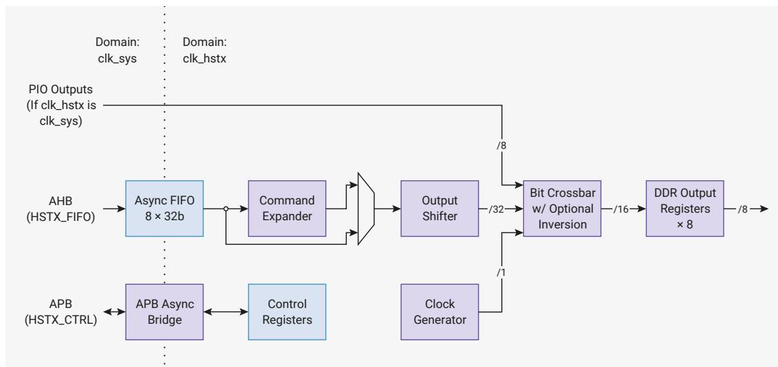
HSTX drives data through GPIOs using DDR output registers to transfer up to two bits per clock cycle per pin. The HSTX balances all delays to GPIO outputs within 300 picoseconds, minimising common-mode components when using neighbouring GPIOs as a pseudo-differential driver. This also helps maintain destination setup and hold time when a clock is driven alongside the output data.
The maximum frequency for the HSTX clock is 150 MHz, the same as the system clock. With DDR output operation, this
is a maximum data rate of 300 Mb/s per pin. There are no limits on the frequency ratio of the system and HSTX clocks, however each clock must be individually fast enough to maintain your required throughput. Very low system clock frequencies coupled with very high HSTX frequencies might encounter system DMA bandwidth limitations, since the DMA is capped at one HSTX FIFO write per system clock cycle.
12.11.1. Data FIFO
An 8-entry, 32-bit-wide FIFO buffers data between the system clock domain (
clk_sys
) and the HSTX clock domain (
clk_hstx
). This is accessed through the AHB
FASTPERI
arbiter, providing single-cycle write access from the DMA. The FIFO status is also available through this same bus interface, for faster polled processor IO; see
Section 12.11.8
.
The FIFO is accessed through a bus interface separate from the control registers (
Section 12.11.7
), which take multiple cycles to access due to the asynchronous bus crossing. This design avoids incurring bus stalls on the system DMA or the
FASTPERI
arbiter when accessing the FIFO.
The HSTX side also pops 32 bits at a time from the FIFO. The word data stream from the FIFO is optionally manipulated by the command expander ( Section 12.11.5 ) before being passed to the output shift register.
12.11.2. Output shift register
Figure 127. Every cycle, the output shift register either refills 32 bits from the FIFO or recirculates data through a right-rotate function. The rotate can be used to perform left or right shifts, and to repeat data.
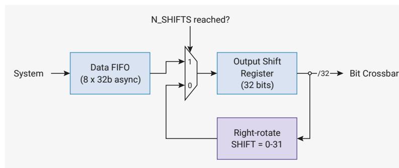
graph LR
    System --> DataFIFO[Data FIFO 8 x 32b async]
    DataFIFO --> Mux{ }
    Mux -- 1 --> OSR[Output Shift Register 32 bits]
    Mux -- 0 --> RR[Right-rotate SHIFT = 0-31]
    OSR --> RR
    RR --> Mux
    Mux -- N_SHIFTS reached? --> OSR
    OSR -- /32 --> BC[Bit Crossbar]
The HSTX's internal data paths are 32 bits wide, but the output is narrower: no more than 16 bits can be output per HSTX cycle (8 GPIOs × DDR). The output shift register adapts these mismatched data widths. The output shift register is a 32-bit shift register, which always refills 32 bits at a time, either from the command expander output or directly from the data FIFO.
The source of data for the output shift register is configured by the
CSR.EXPAND_EN
field:
- • when set, the command expander interposes the FIFO and the output shift register
- • when clear, the command expander is bypassed, popping the FIFO directly into the shift register
Whenever
CSR.EN
is low, the shift register is flushed to empty. Once HSTX has been configured, and
EN
is set high, the shift register is ready to accept data, and will pop data as soon as it becomes available.
After popping the first data word, the shift register will now shift every HSTX clock cycle until it becomes empty. The shift behaviour is configured by:
- •
CSR.N_SHIFTS, which determines how many times to shift before the register is considered empty - •
CSR.SHIFT, which is a right-rotate applied to the shift register every cycle
CSR.N_SHIFTS
and
CSR.SHIFT
must only be changed when
CSR.EN
is low. It is safe to change these fields in the same register write that sets
EN
from low to high.
\(
\text{SHIFT} \times \text{N\_SHIFTS}
\)
is not necessarily less than or equal to 32. For example, a
SHIFT
of 31 might be used to shift the register left by one bit per cycle, since right-rotate is a modular operation, and -1 is equal to 31 under a modulus of 32.
When the shift register is about to become empty, it will immediately refill with fresh data from the command expander or FIFO if data is available. When data is available, the shift register is never empty for any cycle. If data is not available,
the shift register becomes empty and stops shifting until more data is provided. Once data is provided, the shift register refills and begins shifting once again.
12.11.3. Bit crossbar
The bit crossbar controls which bits of the output shift register appear on which GPIOs during the first and second half of each HSTX clock cycle. There is a configuration register for each pin, BIT0 through BIT7 :
- • BITx.SEL_P selects which shift register bit (0 through 31) is output for the first half of each HSTX clock cycle
- • BITx.SEL_N selects which shift register bit (0 through 31) is output for the second half of each clock cycle
- • BITx.INV inverts the output (logical NOT)
- • BITx.CLK indicates that this pin should be connected to the clock generator ( Section 12.11.4 ) rather than the output shift register
To disable DDR behaviour set SEL_N equal to SEL_P . To implement a differential output, configure two pins identically except for the INV bit, which should be set for one pin and clear for the other.
12.11.3.1. Examples: one pin
Together with the SHIFT and N_SHIFTS controls for the shift register, the pin configuration determines the data layout passed through the HSTX. Since not all of us are accustomed to thinking in four dimensions, it's worth going through some examples with a single pin:
- • N_SHIFTS = 32, SHIFT = 1, SEL_P = 0, SEL_N = 0:
- •
N_SHIFTS
= 32,
SHIFT
= 31,
SEL_P
= 31,
SEL_N
= 31:
- ◦ Shift out one bit per HSTX clock cycle, MSB-first.
- ◦ Each cycle, the shift register advances to the left by one (or rather, wraps around the right-hand edge of the register and ends up one bit left of where it started), and the most-significant bit at that time is presented to the pin.
- •
N_SHIFTS
= 16,
SHIFT
= 2,
SEL_P
= 0,
SEL_N
= 1:
- ◦ Shift out two bits per HSTX clock cycle, LSB-first.
- ◦ Each cycle, the shift register advances to the right by two. The least-significant bit is presented to the pin for the first half of that cycle, and the neighbouring bit is presented for the second half.
- •
N_SHIFTS
= 16,
SHIFT
= 30,
SEL_P
= 31,
SEL_N
= 30:
- ◦ Shift out two bits per HSTX clock cycle, MSB-first.
- ◦ Each cycle, the shift register advances to the left by two. The most-significant bit is presented to the pin for the first half of that cycle, and the neighbouring bit is presented for the latter half.
- •
N_SHIFTS
= 8,
SHIFT
= 4,
SEL_P
= 0,
SEL_N
= 0:
- ◦ Shift out the least-significant bit in each group of 4 bits, over the course of 8 clock cycles.
- ◦ Each cycle, the shift register advances to the right by four. The least-significant bit of the shift register is presented to the pin. The bit indices presented to the pin are therefore 0, 4, 8, 12, 16, 20, 24, and 28.
- • N_SHIFTS = 32, SHIFT = 4, SEL_P = 0, SEL_N = 0:
- ◦ Same as the previous, but repeats the 8-cycle pattern four times before refreshing the shift register.
- ◦ Rotating by 32 restores the original value that was popped into the shift register from the FIFO or command expander.
12.11.3.2. Examples: multiple pins
The separation of shift register and bit crossbar allows both zipped and unzipped multi-bit records, once multiple pins are involved. For example, compare these two configurations:
- •
N_SHIFTS = 8, SHIFT = 4, BIT0.SEL_P = 0, BIT0.SEL_N = 2, BIT1.SEL_P = 1, BIT1.SEL_N = 3:- ◦ Each 32-bit word consists of 16 bit-pairs, and a new bit-pair is presented to
BIT0andBIT1twice per cycle. - ◦ The shift register advances by 4 every cycle, introducing two new bit-pairs to the rightmost four bits of the shift register
- ◦ Each 32-bit word consists of 16 bit-pairs, and a new bit-pair is presented to
- •
N_SHIFTS = 8, SHIFT = 2, BIT0.SEL_P = 0, BIT0.SEL_N = 1, BIT1.SEL_P = 16, BIT1.SEL_N = 17:- ◦ Each 32-bit word consists of a pair of 16-bit values, each of which is shifted to one pin out of
BIT0andBIT1at a rate of two bits per cycle. - ◦ The shift register advances by two every cycle, introducing a new bit-pair to bits 1:0 for the
BIT0pin, and also introducing a new bit-pair to bits 17:16 for theBIT1pin.
- ◦ Each 32-bit word consists of a pair of 16-bit values, each of which is shifted to one pin out of
Depending on software needs, it might be preferable to pack together all of the bits output on the same cycle (zipped records), or all of the bits that go through the same pin (unzipped records), so HSTX supports both.
As a final, concrete example, take TMDS (used in DVI): here each 32-bit word contains \( 3 \times 10 \) -bit TMDS symbols, each of which is serialised to a differential pair over the course of 10 TMDS bit times. For performance, it's preferable to make each HSTX clock period equal to two TMDS bit periods, by leveraging the DDR capability. A possible configuration would therefore be:
- •
CSR: N_SHIFTS = 5, SHIFT = 2 - •
BIT0: SEL_P = 0, SEL_N = 1, INV = 0 - •
BIT1: SEL_P = 0, SEL_N = 1, INV = 1 - •
BIT2: SEL_P = 10, SEL_N = 11, INV = 0 - •
BIT3: SEL_P = 10, SEL_N = 11, INV = 1 - •
BIT4: SEL_P = 20, SEL_N = 21, INV = 0 - •
BIT5: SEL_P = 20, SEL_N = 21, INV = 1
The missing piece for TMDS is the clock, which has a period of 10 TMDS bit periods, or 5 HSTX clock periods when shifting two bits per cycle per pin. HSTX has a special-purpose clock generator so that pseudo-clock bits do not have to be packed into the FIFO data stream. The clock generator is covered in the next section.
12.11.4. Clock generator
The clock generator is a counter that provides a periodic signal over the course of
n
HSTX clock cycles, configured by
CSR.CLKDIV
. The clock period is always an integer number of HSTX clock cycles, in the range 1 to 16 inclusive. The clock generator supports both odd and even periods, using the DDR outputs to support mid-HSTX-cycle output transitions. There is only a single clock generator — to emulate multiple clocks, pack pseudo-clock bits into FIFO data.
The clock generator increments on cycles where the output shift register is shifted. Generally, the clock period will be a divisor of
CSR.N_SHIFTS
so that clock and data maintain a consistent alignment. In the TMDS example in the previous section, a
CLKDIV
of 5 would be suitable, so that the clock repeats every time the shift register refreshes. This matches the requirement for a TMDS clock period of 10 bit periods, since two bits are transferred every cycle.
The clock generator output is connected to any pin whose
BITx.CLK
bit is set (e.g.
BIT0.CLK
). To produce differential
clock outputs, connect the clock to two pins, and invert one of them.
The
CSR.CLKPHASE
field defines the initial phase (count) of the clock generator, configured in units of one half HSTX clock cycle. The clock generator resets whenever
CSR.EN
is low and holds at this initial phase. Once
CSR.EN
is set and the output shift register begins to shift, the clock generator advances.
Clock generator output whilst
CSR.EN
is low is determined by the relation of clock period and initial clock phase: if the initial clock phase is less than one half clock period, then the output is initially low. Otherwise, it is initially high. The clock generator can be thought of as being low for the first half of each generation period, and high for the second half.
The maximum
CSR.CLKPHASE
is only 15
half
HSTX clock cycles. The maximum
CSR.CLKDIV
is 16
full
HSTX clock cycles: initial phases of greater than or equal to 180 degrees with the maximum clock period require the inversion of the clock using the bit crossbar inversion controls.
Only change
CSR.CLKPHASE
and
CSR.CLKDIV
when
CSR.EN
is low. It is safe to modify them in the same register write that sets
EN
from low to high.
12.11.4.1. Example: centre-aligned clock
When transmitting source-synchronous data, the data sink (the receiver) must not see data transitions too late before or too soon after the active edges of the clock. Violating these setup and hold constraints can lead to undefined operation of the external data sink.
Since the HSTX output delays are all mutually balanced, you can meet these constraints by placing clock transitions halfway between data transitions, known as centre-aligned clocking.
Since this positions the clock with a temporal resolution of one half of a bit time, the maximum data rate is one bit per HSTX clock cycle per pin. Because the clock already uses DDR, you cannot use DDR to increase the data rate. Therefore for all
BIT0
through
BIT7
,
BITx.SEL_N
is equal to
BITx.SEL_P
.
For single-data-rate data, with an active rising edge, use the following clock generator settings:
- •
CSR.CLKDIV= 1 (1 HSTX clock period) - •
CSR.CLKPHASE= 1 (1/2 HSTX clock period)
The clock is delayed by half an HSTX cycle, to offset it from the launch of the first data.
For single-data-rate data, with an active falling edge, use the following clock generator settings:
- •
CSR.CLKDIV= 1 (1 HSTX clock period) - •
CSR.CLKPHASE= 2 (1 HSTX clock period)
Alternatively, you could use the same settings as an active-rising edge clock, with the clock output inverted via the bit crossbar configuration.
For double-data-rate data, with active rising and active falling edges, use the following clock generator settings:
- •
CSR.CLKDIV= 2 (2 HSTX clock period) - •
CSR.CLKPHASE= 1 (1/2 HSTX clock period)
In all three cases, the data rate is the same, at 1 bit per HSTX clock cycle, per pin.
12.11.5. Command expander
Figure 128. A mixture of commands and data are popped from the FIFO. Data can be repeated or shifted through the expansion shift register, and optionally passed through an encoder before passing on to the output shift register.
graph LR
    FIFO[From FIFO] --> Split1(( ))
    Split1 --> CCR[Command + Count Register 16 bits]
    Split1 --> Split2(( ))
    Split2 --> ESR[Expansion Shift Register 32 bits]
    Split2 --> Split3(( ))
    Split3 --> RR[Right-rotate x_SHIFT 0 to 31]
    Split3 --> Encoder[Encoder]
    ESR --> Encoder
    RR --> Encoder
    Encoder --> OSR[To output shift register]
The command expander can be inserted inline between the data FIFO and the output shift register to manipulate the stream of data words. In general, the output stream is larger than the input stream, hence the name expander. The command expander is enabled by setting
CSR.EXPAND_EN
. Only modify this field when
CSR.EN
is low. It is safe to modify this field in the same register write that sets
EN
from low to high. When the command expander is disabled, data passes directly from the data FIFO to the output shift register without being modified by the expander.
When the command expander is enabled, the data FIFO carries a mixture of data and commands for the expander. Each command consists of a 4-bit opcode and a 12-bit length, packed in the 16 LSBs of a data FIFO word, with the opcode in bits 15 through 12, and the length in bits 11 through 0. The available commands are:
- •
0x0: RAW - •
0x1: RAW_REPEAT - •
0x2: TMDS - •
0x3: TMDS_REPEAT - •
0xf: NOP
When the HSTX is first enabled, if the command expander is enabled, it expects the first word in the data FIFO to be a command. If this command is not a
NOP
, it will be followed by some amount of data, then another command. Operation continues in this manner, with runs of data interspersed with commands. A command always acts as a prefix to the data that follows it in the FIFO.
The count field determines the number of words output by this command to the output shift register downstream, from 1 to 4095. A count of 0 is reserved to mean "infinite". The number of words that this command reads from the data FIFO in order to produce the specified quantity of downstream data depends on the command and the
EXPAND_SHIFT.ENC_N_SHIFTS
and
EXPAND_SHIFT.RAW_N_SHIFTS
register fields.
The expansion shift register always pops from the FIFO once at the beginning of the command. After this point, commands bearing the
x_REPEAT
suffix continue to circulate the same contents through the shift register, rotating right by
EXPAND_SHIFT.ENC_SHIFT
or
EXPAND_SHIFT.RAW_SHIFT
each time the output shift register pulls new data from the command expander. Use a shift of 0 to repeat identical data without shifting. This is useful, for example, for transmitting runs of the same TMDS control symbol during horizontal blanking periods in DVI.
RP2350 only implements a TMDS encoder, reserving the remaining opcode space for additional encoders in the future.
RAW
and
RAW_REPEAT
commands bypass the encoder.
TMDS
and
TMDS_REPEAT
commands are TMDS-encoded before being passed to the output shift register.
NOP
commands have no data, therefore whether they bypass the encoder or not is a philosophical question beyond the scope of this datasheet.
The
EXPAND_SHIFT
register has two copies for each of its fields. Fields prefixed with
RAW_
are used for
RAW
and
RAW_REPEAT
commands. All other commands use fields prefixed with
ENC_
, which pass through the encoder. For example, in DVI, TMDS control symbols using
RAW_REPEAT
commands may be unshifted. Pixel data using TMDS commands may be shifted out one pixel at a time, so it is useful to have banked shift controls.
The
EXPAND_SHIFT.ENC_N_SHIFTS
and
EXPAND_SHIFT.RAW_N_SHIFTS
fields control how often the expansion shift register is refilled for encoded and raw commands respectively.
x_REPEAT
commands ignore these fields since they never refill from the FIFO, and function similarly to the
CSR.N_SHIFTS
field that controls the output shift register.
The command expander can only pop from the data FIFO once per cycle, so heavy use of commands (particularly
NOP
commands) can impact HSTX throughput. For use cases that output from the HSTX on every cycle, configure the output shift register with
CSR.N_SHIFTS > 1
. This is required because the command expander cannot output data on the cycle where it pops a command from the FIFO, so the expansion shift register is empty for at least one cycle.
12.11.6. PIO-to-HSTX coupled mode
HSTX can connect up to 8 PIO pin outputs to the bit crossbar. Only use the bit crossbar when
clk_hstx
connects directly to
clk_sys
(
CLK_HSTX_CTRL.AUXSRC
must select
clk_sys
).
NOTE
Running the two clocks at the same frequency is not sufficient. You must select
clk_sys
directly.
To enable coupled mode, set
CSR.COUPLED_MODE
. The
COUPLED_SEL
field in the same register selects the PIO instance, 0 through 2, to couple to HSTX. When coupled mode is enabled, IO outputs 12 through 19 inclusive on the selected PIO instance appear at bit crossbar
PSEL_N
and
PSEL_P
indices 31:24, replacing the most significant 8 bits of the output shift register from the point of view of the bit crossbar.
This mode allows PIO programs to make use of the HSTX's DDR outputs. You can use this mode to drive a clock at the full system clock rate or to position clock transitions relative to data transitions with half-system-clock-cycle resolution.
The PIO outputs used for couple mode are always bits 19 through 12 of the pin outputs driven from that GPIO, independent of
GPIOBASE
. When
GPIOBASE
is 0, the PIO outputs used for coupled mode are those that would normally appear on the
HSTX
pins. When
GPIOBASE
is 16, this uses the PIO outputs that would appear on GPIOs 28 through 35.
The operation of PIO is not affected in any way by coupled mode being enabled.
Outputs presented through the HSTX coupled mode interface have one additional system clock cycle of delay compared to those presented directly from PIO to the pads.
12.11.7. List of control registers
The control registers start at a base address of
0x400c0000
(defined as
HSTX_CTRL_BASE
in the SDK). They are accessed through an asynchronous bus crossing, so each bus access takes several cycles, the exact figure depending on the ratio of
clk_sys
and
clk_hstx
.
Table 1253. List of HSTX_CTRL registers
| Offset 0x42fc8 0x42fcc 0x42fd0 0x42fd4 0x42fd8 | Name DEVID DEVTYPE PIDR4 PIDR5 PIDR6 | Info Device Configuration register Device Type Identifier register CoreSight Periperal ID4 CoreSight Periperal ID5 CoreSight Periperal ID6 |
|---|---|---|
| shift register with | CSR .N_SHIFTS > 1. This is required because the command expander cannot output data on the cycle | |
| HSTX can connect up to 8 PIO pin outputs to the bit crossbar. Only use the bit crossbar when | clk_hstx connects directly | |
| to clk_sys ( CLK_HSTX_CTRL NOTE | .AUXSRC must select | clk_sys). |
| To enable coupled mode, set | CSR. | COUPLED_MODE. The COUPLED_SEL field in the same register selects the PIO instance, |
| instance appear at bit crossbar | PSEL_N and PSEL_P register from the point of view of the bit crossbar. | indices 31:24, replacing the most significant 8 bits of the output shift |
| independent of | GPIOBASE . When | GPIOBASE is 0, the PIO outputs used for coupled mode are those that would normally |
| appear on the | HSTX pins. When GPIOBASE | is 16, this uses the PIO outputs that would appear on GPIOs 28 through 35. |
| The control registers start at a base address of | 0x400c0000 (defined as HSTX_CTRL_BASE in the SDK). They are | |
| on the ratio of on the ratio of Table 1253. List of | clk_sys and clk_hstx. clk_sys and clk_hstx. | |
| Offset HSTX_CTRL registers | Name | Info |
| 0x00 0x00 | CSR CSR | |
| 0x04 | BIT0 | Data control register for output bit 0 |
| 0x08 | BIT1 | Data control register for output bit 1 |
| 0x0c | BIT2 | Data control register for output bit 2 |
| 0x10 | BIT3 | Data control register for output bit 3 |
| 0x14 | BIT4 | Data control register for output bit 4 |
| 0x18 | BIT5 | Data control register for output bit 5 |
| 0x1c | BIT6 | Data control register for output bit 6 |
| 0x20 | BIT7 | Data control register for output bit 7 |
| 0x24 | EXPAND_SHIFT | Configure the optional shifter inside the command expander |
| 0x28 | EXPAND_TMDS | Configure the optional TMDS encoder inside the command expander |
HSTX_CTRL: CSR Register
Offset: 0x00
Table 1254. CSR Register
| Bits | Description | Type | Reset |
|---|---|---|---|
| 31:28 | CLKDIV: Clock period of the generated clock, measured in HSTX clock cycles. Can be odd or even. The generated clock advances only on cycles where the shift register shifts. For example, a clkdiv of 5 would generate a complete output clock period for every 5 HSTX clocks (or every 10 half-clocks). A CLKDIV value of 0 is mapped to a period of 16 HSTX clock cycles. | RW | 0x1 |
| 27:24 | CLKPHASE: Set the initial phase of the generated clock. A CLKPHASE of 0 means the clock is initially low, and the first rising edge occurs after one half period of the generated clock (i.e. CLKDIV/2 cycles of clk_hstx). Incrementing CLKPHASE by 1 will advance the initial clock phase by one half clk_hstx period. For example, if CLKDIV=2 and CLKPHASE=1:
This configuration would be suitable for serialising at a bit rate of clk_hstx with a centre-aligned DDR clock. When the HSTX is halted by clearing CSR_EN, the clock generator will return to its initial phase as configured by the CLKPHASE field. Note CLKPHASE must be strictly less than double the value of CLKDIV (one full period), else its operation is undefined. | RW | 0x0 |
| 23:21 | Reserved. | - | - |
| 20:16 | N_SHIFTS: Number of times to shift the shift register before refilling it from the FIFO. (A count of how many times it has been shifted, not the total shift distance.) A register value of 0 means shift 32 times. | RW | 0x05 |
| 15:13 | Reserved. | - | - |
| 12:8 | SHIFT: How many bits to right-rotate the shift register by each cycle. The use of a rotate rather than a shift allows left shifts to be emulated, by subtracting the left-shift amount from 32. It also allows data to be repeated, when the product of SHIFT and N_SHIFTS is greater than 32. | RW | 0x06 |
| 7 | Reserved. | - | - |
| 6:5 | COUPLED_SEL: Select which PIO to use for coupled mode operation. | RW | 0x0 |
| Bits Register 31:21 20 19:16 15:12 11:0 | column_2 | Description ARCHITECT : Defines the architect of the component. Bits [31:28] are the PRESENT : Defines that the DEVARCH register is present REVISION : Defines the architecture revision of the component ARCHVER : Defines the architecture version of the component ARCHPART : Defines the architecture of the component | Type RO RO RO RO RO | Reset 0x23b 0x1 0x0 0x1 0xa02 |
|---|---|---|---|---|
| 3:2 | Reserved. | - | - | |
| 1 | EXPAND_EN | : Enable the command expander. When 0, raw FIFO data is | RW | 0x0 |
| 0 | EN | simultaneously with setting EN. : When EN is 1, the HSTX will shift out data as it appears in the FIFO. As long as there is data, the HSTX shift register will shift once per clock cycle, and the frequency of popping from the FIFO is determined by the ratio of | RW | 0x0 |
| Table 1255. BIT0, Bits BIT1, …, BIT6, BIT7 | Description | Type | Reset | |
| Registers 31:18 | Reserved. | - | - | |
| 17 | CLK | : Connect this output to the generated clock, rather than the data shift to generate an antiphase clock. | RW | 0x0 |
| 16 | INV | : Invert this data output (logical NOT) | RW | 0x0 |
| 15:13 | Reserved. | - | - | |
| 12:8 | SEL_N | : Shift register data bit select for the second half of the HSTX clock cycle | RW | 0x00 |
HSTX_CTRL: BIT0, BIT1, ..., BIT6, BIT7 Registers
Offsets: 0x04, 0x08, ..., 0x1c, 0x20
Description
Data control register for output bit n
Table 1255. BIT0, BIT1, ..., BIT6, BIT7 Registers
| Bits 31:0 Bits 31:0 Bits 31:28 | column_2 | Description Description Input value for GPIO0…31. Description QSPI_SD : Input value on QSPI SD0 (MOSI), SD1 (MISO), SD2 and SD3 pins | Type RO Type RO Type RO | Reset - Reset 0x00000000 Reset 0x0 |
|---|---|---|---|---|
| 7:5 | Reserved. | - | - | |
| 4:0 | SEL_P | : Shift register data bit select for the first half of the HSTX clock cycle | RW | 0x00 |
| Table 1256. Bits EXPAND_SHIFT | Description | Type | Reset | |
| Register 31:29 | Reserved. | - | - | |
| 28:24 | ENC_N_SHIFTS | : Number of times to consume from the shift register before refilling it from the FIFO, when the current command is an encoded data command (e.g. TMDS). A register value of 0 means shift 32 times. | RW | 0x01 |
| 23:21 | Reserved. | - | - | |
| 20:16 | ENC_SHIFT | : How many bits to right-rotate the shift register by each time data command (e.g. TMDS). | RW | 0x00 |
| 15:13 | Reserved. | - | - | |
| 12:8 | RAW_N_SHIFTS | : Number of times to consume from the shift register before A register value of 0 means shift 32 times. | RW | 0x01 |
| 7:5 | Reserved. | - | - | |
| 4:0 | RAW_SHIFT | : How many bits to right-rotate the shift register by each time data is pushed to the output shifter, when the current command is a raw data command. | RW | 0x00 |
| Table 1257. Bits EXPAND_TMDS | Description | Type | Reset | |
| Register 31:24 | Reserved. | - | - | |
| 23:21 | L2_NBITS | : Number of valid data bits for the lane 2 TMDS encoder, starting | RW | 0x0 |
| from bit 7 of the rotated data. Field values of 0 bits. | → 7 encode counts of 1 → 8 | |||
| 20:16 | L2_ROT | : Right-rotate applied to the current shifter data before the lane 2 TMDS encoder. | RW | 0x00 |
| 15:13 | L1_NBITS | : Number of valid data bits for the lane 1 TMDS encoder, starting | RW | 0x0 |
| from bit 7 of the rotated data. Field values of 0 bits. | → 7 encode counts of 1 → 8 | |||
| 12:8 | L1_ROT | : Right-rotate applied to the current shifter data before the lane 1 TMDS encoder. | RW | 0x00 |
HSTX_CTRL: EXPAND_SHIFT Register
Offset: 0x24
Description
Configure the optional shifter inside the command expander
Table 1256.
EXPAND_SHIFT
Register
HSTX_CTRL: EXPAND_TMDS Register
Offset: 0x28
Description
Configure the optional TMDS encoder inside the command expander
Table 1257.
EXPAND_TMDS
Register
| Bits | Description | Type | Reset |
|---|---|---|---|
| 7:5 | L0_NBITS : Number of valid data bits for the lane 0 TMDS encoder, starting from bit 7 of the rotated data. Field values of 0 → 7 encode counts of 1 → 8 bits. | RW | 0x0 |
| 4:0 | L0_ROT : Right-rotate applied to the current shifter data before the lane 0 TMDS encoder. | RW | 0x00 |
12.11.8. List of FIFO registers
The FIFO registers start at a base address of 0x50600000 (defined as
HSTX_FIFO_BASE
in the SDK).
Table 1258. List of HSTX_FIFO registers
| Offset | Name | Info |
|---|---|---|
| 0x0 | STAT | FIFO status |
| 0x4 | FIFO | Write access to FIFO |
HSTX_FIFO: STAT Register
Offset: 0x0
Description
FIFO status
Table 1259. STAT Register
| Bits | Description | Type | Reset |
|---|---|---|---|
| 31:11 | Reserved. | - | - |
| 10 | WOF : FIFO was written when full. Write 1 to clear. | WC | 0x0 |
| 9 | EMPTY | RO | - |
| 8 | FULL | RO | - |
| 7:0 | LEVEL | RO | 0x00 |
HSTX_FIFO: FIFO Register
Offset: 0x4
Table 1260. FIFO Register
| Bits | Description | Type | Reset |
|---|---|---|---|
| 31:0 | Write access to FIFO | WF | 0x00000000 |
12.12. TRNG
12.12.1. Overview
RP2350 contains an Arm IP-based True Random Number Generator block. It supports the following features:
- • Compliance with FIPS Publication 140-2, BSI AIS-31, and NIST SP 800-90B
- • Produces approximately 7.5 kb/s of entropy when the core runs at 150 MHz
On request, the TRNG block generates a block of 192 entropy bits generated by automatically processing a series of periodic samples from the TRNG block’s internal Ring Oscillator (ROSC).
The TRNG block's ROSC is a free-running oscillator with no direct connection to the system clocks on RP2350. As a result, the ROSC generally runs asynchronously to the system clocks.
After a sufficient number of samples have been collected, the TRNG block completes the generation process and presents the random number in the
EHR_DATA[x]
result registers.
For more information, see ARM IP - True Random Number Generator
12.12.2. Configuration
The TRNG block contains three different built-in entropy checking mechanisms: At reset, these are all enabled by default and hence do not require explicit enabling.
You can configure the TRNG block in the following ways:
- • Configure the frequency of the ROSC by selecting of one of four ROSC chain lengths , see TRNG_CONFIG .
- • Configure the ROSC sampling period in terms of system clock ticks, see SAMPLE_CNT1 .
Because the system clock generally runs much faster than the ROSC, the sampling period is expected to be at least a few tens of system clock ticks.
Because the characteristics of the TRNG ROSC and system clock frequency will differ for each implementation of the TRNG IP block, Arm details a TRNG characterisation procedure to determine the most appropriate ROSC chain length and sampling frequency settings on each SoC design. For details about that characterisation procedure, see ARM TrustZone True Number Generator .
Software drivers for the RP2350 TRNG block do not utilise the standard approach (see Section 12.12.4 ). As a result, software does not configure the ROSC length and sample count settings provided by the Arm characterisation procedure.
When configuring the TRNG block, consider the following principles:
- • As average generation time increases, result quality increases and failed entropy checks decrease.
- • A low sample count decreases average generation time, but increases the chance of NIST test-failing results and failed entropy checks.
For acceptable results with an average generation time of about 2 milliseconds, use ROSC chain length settings of 0 or 1 and sample count settings of 20-25.
Larger sample count settings (e.g. 100) provide proportionately slower average generation times. These settings significantly reduce, but do not eliminate NIST test failures and entropy check failures. Results occasionally take an especially long time to generate.
12.12.3. Operation
To initiate TRNG generation, set the
RND_SRC_EN
bit in
RND_SOURCE_ENABLE
. The TRNG will run until:
- • It has successfully completed the generation of a random number.
- • One, or more, of the internal entropy checking mechanisms indicates a failed run.
In either case, you can read the resultant status from RNG_ISR .
To generate TRNG block interrupts, set bits in RNG_IMR . Use RNG_ICR to clear active interrupt status bits.
The
EHR_DATA[x]
registers read 0 until successful generation has occurred, so the CPU cannot read random number results during generation,
After successful generation, read the last result register,
EHR_DATA[5]
to clear all of the result registers. If the result fails an entropy check, no results are presented and the
EHR_DATA[x]
registers all read as 0.
After TRNG generation and when not in use, the
RND_SRC_EN
bit should be cleared.
12.12.4. Caveats
The generation of random numbers by the TRNG block is not a deterministic process.
Although the modal and mean average times required to generate random numbers are quite similar, the generation process can occasionally take much longer to complete: in excess of 100 times the average. Any run resulting in a failed entropy check discards the result, requiring another generation process.
You can accommodate these unpredictable generation times in your system design. For example, you might generate a small pool of random numbers, initiating subsequent generation whenever space becomes available in the pool.
In the interests of simplicity and timing predictability, alternative approaches were adopted for the RP2350 bootrom and the SDK TRNG block drivers. The methodologies used can be found via the links below. However, nothing in the TRNG block in RP2350 precludes using the block as specified in Arm documentation.
12.12.4.1. Bootrom
The bootrom streams raw TRNG ROSC samples (the TRNG random source) directly into the hardware SHA-256 accelerator. It bypasses all internal checking and conditioning in the TRNG. SHA-256 is a robust hash function which avoids the pitfalls of some of the conditioning logic in the TRNG, most notably the von Neumann decorrelator.
The bootrom has some hard constraints which guide its implementation choices, most notably: the bootrom must boot . It cannot afford to poll the TRNG for an indeterminate amount of time to wait for a random number to appear. Complex error handling is also undesirable.
A link to the bootrom source can be found in
Chapter 5
. Consult the source code for the exact implementation of the per-boot random number generation, in
varm_boot_path.c
.
The A2 bootrom TRNG code is written in assembly due to various implementation constraints, and may not be that illuminating. The following is excerpted from the A1 bootrom source, lightly edited for readability:
// Boot RNG is derived by streaming a large number of TRNG ROSC samples
// into the SHA-256. BOOT_TRNG_SAMPLE_BLOCKS is the number of SHA-256
// blocks to hash, each containing 384 samples from the TRNG ROSC:
const int BOOT_TRNG_SAMPLE_BLOCKS = 25;

// Fixed delay is required after TRNG soft reset
trng_hw->trng_sw_reset = -1u;
(void)trng_hw->trng_sw_reset;
(void)trng_hw->trng_sw_reset;
// Initialise SHA internal state by writing START bit
sha256_hw->csr = SHA256_CSR_RESET | SHA256_CSR_START_BITS;

// Sample one ROSC bit into EHR every cycle, subject to CPU keeping up. More
// temporal resolution to measure ROSC phase noise is better, if we use a
// high quality hash function instead of naive VN decorrelation. (Also more
// metastability events, which are a secondary noise source)
trng_hw->sample_cnt1 = 0;
// Disable checks and bypass decorrelators, to stream raw TRNG ROSC samples:
trng_hw->trng_debug_control = -1u;
// Start ROSC if it is not already started
trng_hw->rnd_source_enable = -1u;
// Clear all interrupts (including EHR_VLD) -- we will check this
// later, after seeding RCP.
trng_hw->rng_icr = -1u;

// Each half-block (192 samples) takes approx 235 cycles, so 470 cycles/block:
for (int half_blocks = 0; half_blocks < 2 * BOOT_TRNG_SAMPLE_BLOCKS; ++half_blocks) {

    // Wait for 192 ROSC samples to fill EHR, this should take constant time:
    while (trng_hw->trng_busy)
;

// Copy 6 EHR words to SHA-256, plus garbage (RND_SOURCE_ENABLE and
// SAMPLE_CNT1) which pads us out to half of a SHA-256 block. This means
// we can avoid checking SHA-256 ready whilst reading EHR, so we restart
// sampling sooner. (SHA-256 becomes non-ready for 57 cycles after each
// 16 words written.)
io_ro_32 *src = &trng_hw->ehr_data[0];
io_wo_32 *dst = &sha256_hw->wdata;
for (int i = 0; i < 8; ++i) {
    *dst = src[i];
}

// TRNG is now sampling again, having started after we read the last EHR
// word. Grab some in-progress SHA bits and use them to modulate the
// chain length, to reduce chance of injection locking:
trng_hw->trng_config = sha256_hw->sum[0];
}

// Wait for SHA result -- if skipped we get the previous block's digest. Note
// this never becomes true if we wrote a number of words % 16 != 0.
while (!(sha256_hw->csr & SHA256_CSR_SUM_VLD_BITS))
    ;

// The per-boot random will change on every core 0 reset (except debugger
// skipping ROM). If this is a problem then the user can sample the
// per-boot random into a preserved variable in main SRAM.
for (int i = 0; i < 4; ++i) {
    bootram->always.boot_random.e[i] = sha256_hw->sum[4 + i];
}

trng_hw->trng_config = 0;
// Stop ROSC as it's a waste of power
trng_hw->rnd_source_enable = 0;
The bootrom resets the SHA-256 and TRNG via RESETS immediately before the above code runs. This code typically runs with
clk_sys
running from the system ROSC, at its initial boot frequency of approximately 12 MHz. The 256-bit result is available in the
SUM0
through
SUM7
registers after the code completes.
This code does not represent best programming practice: for example it writes ones into reserved bits in the
TRNG_DEBUG_CONTROL
register. It was written with close reference to the hardware implementation. The above code listing serves only to document the
method
the bootrom uses to generate random numbers at boot time, for the once-per-boot random number available via the
get_sys_info()
ROM API as well as for initialising the RCP salt registers (Section 3.6.3.1).
12.12.4.2. SDK
The
pico_rand
library uses the TRNG as one of its entropy sources. It streams raw ROSC samples from the TRNG ROSC in a similar manner to the bootrom. It uses the
xoroshiro128**
and
splitmix64()
PRNG functions to condition the output.
12.12.5. List of registers
The TRNG control registers start at a base address of
0x400f0000
(defined as
TRNG_BASE
in the SDK).
Table 1261. List of TRNG registers
| Offset | Name | Info |
|---|---|---|
| 0x100 | RNG_IMR | Interrupt masking. |
| Offset | Name | Info |
|---|---|---|
| 0x104 | RNG_ISR | RNG status register. If corresponding RNG_IMR bit is unmasked, an interrupt will be generated. |
| 0x108 | RNG_ICR | Interrupt/status bit clear Register. |
| 0x10c | TRNG_CONFIG | Selecting the inverter-chain length. |
| 0x110 | TRNG_VALID | 192 bit collection indication. |
| 0x114 | EHR_DATA0 | RNG collected bits. |
| 0x118 | EHR_DATA1 | RNG collected bits. |
| 0x11c | EHR_DATA2 | RNG collected bits. |
| 0x120 | EHR_DATA3 | RNG collected bits. |
| 0x124 | EHR_DATA4 | RNG collected bits. |
| 0x128 | EHR_DATA5 | RNG collected bits. |
| 0x12c | RND_SOURCE_ENABLE | Enable signal for the random source. |
| 0x130 | SAMPLE_CNT1 | Counts clocks between sampling of random bit. |
| 0x134 | AUTOCORR_STATISTIC | Statistics about autocorrelation test activations. |
| 0x138 | TRNG_DEBUG_CONTROL | Debug register. |
| 0x140 | TRNG_SW_RESET | Generate internal SW reset within the RNG block. |
| 0x1b4 | RNG_DEBUG_EN_INPUT | Enable the RNG debug mode |
| 0x1b8 | TRNG_BUSY | RNG Busy indication. |
| 0x1bc | RST_BITS_COUNTER | Reset the counter of collected bits in the RNG. |
| 0x1c0 | RNG_VERSION | Displays the version settings of the TRNG. |
| 0x1e0 | RNG_BIST_CNTR_0 | Collected BIST results. |
| 0x1e4 | RNG_BIST_CNTR_1 | Collected BIST results. |
| 0x1e8 | RNG_BIST_CNTR_2 | Collected BIST results. |
TRNG: RNG_IMR Register
Offset: 0x100
Description
Interrupt masking.
Table 1262. RNG_IMR Register
| Bits | Description | Type | Reset |
|---|---|---|---|
| 31:4 | Reserved. | - | - |
| 3 | VN_ERR_INT_MASK: Set to 1 to mask (disable) this interrupt: no interrupt will be generated. See RNG_ISR for an explanation on this interrupt. | RW | 0x1 |
| 2 | CRNGT_ERR_INT_MASK: Set to 1 to mask (disable) this interrupt: no interrupt will be generated. See RNG_ISR for an explanation on this interrupt. | RW | 0x1 |
| 1 | AUTOCORR_ERR_INT_MASK: Set to 1 to mask (disable) this interrupt: no interrupt will be generated. See RNG_ISR for an explanation on this interrupt. | RW | 0x1 |
| 0 | EHR_VALID_INT_MASK: Set to 1 to mask (disable) this interrupt: no interrupt will be generated. See RNG_ISR for an explanation on this interrupt. | RW | 0x1 |
TRNG: RNG_ISR Register
Offset: 0x104
Description
RNG status register. If corresponding RNG_IMR bit is unmasked, an interrupt will be generated.
Table 1263. RNG_ISR Register
| Bits 14:10 9:5 4:0 Bits | Description SHIFT Description | MASK_MSB : The most-significant bit allowed to pass by the mask (inclusive) MASK_LSB : The least-significant bit allowed to pass by the mask (inclusive) : Right-rotate applied to accumulator before masking. By appropriately | Type RW RW RW Type | Reset 0x00 0x00 0x00 Reset |
|---|---|---|---|---|
| 31:4 | Reserved. | - | - | |
| 3 | VN_ERR | : 1 indicates von Neumann error. Error in von Neumann occurs if 32 | RO | 0x0 |
| 2 | CRNGT_ERR | consecutive collected bits are identical, ZERO or ONE. : 1 indicates CRNGT in the RNG test failed. Failure occurs when | RO | 0x0 |
| 1 | AUTOCORR_ERR | two consecutive blocks of 16 collected bits are equal. : 1 indicates Autocorrelation test failed four times in a row. | RO | 0x0 |
| 0 | EHR_VALID | When set, RNG ceases functioning until next reset. : 1 indicates that 192 bits have been collected in the RNG, and are ready to be read. | RO | 0x0 |
| Bits | Description | Type | Reset | |
| 31:4 | Reserved. | - | - | |
| 3 | VN_ERR | : Write 1 to clear corresponding bit in RNG_ISR. | RW | 0x0 |
| 2 | CRNGT_ERR | : Write 1 to clear corresponding bit in RNG_ISR. | RW | 0x0 |
| 1 | AUTOCORR_ERR | : Cannot be cleared by SW! Only RNG reset clears this bit. | RW | 0x0 |
| 0 | EHR_VALID | : Write 1 - clear corresponding bit in RNG_ISR. | RW | 0x0 |
| Bits | Description | Type | Reset | |
| Register 31:2 | Reserved. | - | - | |
| 1:0 | RND_SRC_SEL | : Selects the number of inverters (out of four possible selections) in the ring oscillator (the entropy source). Higher values select | RW | 0x0 |
TRNG: RNG_ICR Register
Offset: 0x108
Description
Interrupt/status bit clear Register.
Table 1264. RNG_ICR Register
TRNG: TRNG_CONFIG Register
Offset: 0x10c
Description
Selecting the inverter-chain length.
Table 1265. TRNG_CONFIG Register
TRNG: TRNG_VALID Register
Offset: 0x110
Description
192 bit collection indication.
Table 1266.
TRNG_VALID Register
| Bits | Description | Type | Reset |
|---|---|---|---|
| 31:1 | Reserved. | - | - |
| 0 | EHR_VALID : 1 indicates that collection of bits in the RNG is completed, and data can be read from EHR_DATA register. | RO | 0x0 |
TRNG: EHR_DATA0, EHR_DATA1, ..., EHR_DATA4, EHR_DATA5 Registers
Offsets: 0x114, 0x118, ..., 0x124, 0x128
Description
RNG collected bits.
Table 1267.
EHR_DATA0,
EHR_DATA1, ...,
EHR_DATA4,
EHR_DATA5 Registers
| Bits | Description | Type | Reset |
|---|---|---|---|
| 31:0 | Bits \( [(32*(i+1))-1:(32*i)] \) of Entropy Holding Register. | RO | 0x00000000 |
TRNG: RND_SOURCE_ENABLE Register
Offset: 0x12c
Description
Enable signal for the random source.
Table 1268.
RND_SOURCE_ENABLE
Register
| Bits | Description | Type | Reset |
|---|---|---|---|
| 31:1 | Reserved. | - | - |
| 0 | RND_SRC_EN
: * 1 - entropy source is enabled. * 0 - entropy source is disabled | RW | 0x0 |
TRNG: SAMPLE_CNT1 Register
Offset: 0x130
Description
Counts clocks between sampling of random bit.
Table 1269.
SAMPLE_CNT1
Register
| Bits | Description | Type | Reset |
|---|---|---|---|
| 31:0 | SAMPLE_CNTR1
: Sets the number of rng_clk cycles between two consecutive ring oscillator samples. Note: If the von Neumann decorrelator is bypassed, the minimum value for sample counter must not be less than seventeen | RW | 0x0000ffff |
TRNG: AUTOCORR_STATISTIC Register
Offset: 0x134
Description
Statistics about autocorrelation test activations.
Table 1270.
AUTOCORR_STATISTI
C Register
| Bits | Description | Type | Reset |
|---|---|---|---|
| 31:22 | Reserved. | - | - |
| 21:14 | AUTOCORR_FAILS : Count each time an autocorrelation test fails. Any write to the register reset the counter. Stop collecting statistic if one of the counters reached the limit. | RW | 0x00 |
| Bits 2 1 0 Bits | Description RESET PUSH DATA Description | : Reset (before sending a new key) | Type RW RW RW Type | Reset 0x0 0x0 0x0 Reset |
|---|---|---|---|---|
| OL Register 31:4 | Reserved. | - | - | |
| 3 | AUTO_CORRELATE_BYPASS | : When set, the autocorrelation test in the TRNG | RW | 0x0 |
| 2 | TRNG_CRNGT_BYPASS | module is bypassed. : When set, the CRNGT test in the RNG is bypassed. | RW | 0x0 |
| 1 | VNC_BYPASS | : When set, the Von-Neuman balancer is bypassed (including the 32 consecutive bits test). | RW | 0x0 |
| 0 | N/A Reserved. | - | - | |
| Bits | Description | Type | Reset | |
| Register 31:1 | Reserved. | - | - | |
| 0 | TRNG_SW_RESET | : Writing 1 to this register causes an internal RNG reset. | RW | 0x0 |
| Bits | Description | Type | Reset | |
| T Register 31:1 | Reserved. | - | - | |
| 0 | RNG_DEBUG_EN | : * 1 - debug mode is enabled. * 0 - debug mode is disabled | RW | 0x0 |
TRNG: TRNG_DEBUG_CONTROL Register
Offset: 0x138
Description
Debug register.
Table 1271.
TRNG_DEBUG_CONTR
OL Register
TRNG: TRNG_SW_RESET Register
Offset: 0x140
Description
Generate internal SW reset within the RNG block.
Table 1272.
TRNG_SW_RESET
Register
TRNG: RNG_DEBUG_EN_INPUT Register
Offset: 0x1b4
Description
Enable the RNG debug mode
Table 1273.
RNG_DEBUG_EN_INPU
T Register
TRNG: TRNG_BUSY Register
Offset: 0x1b8
Description
RNG Busy indication.
Table 1274.
TRNG_BUSY Register
| Bits 2 1 0 Bits | Description RESET PUSH DATA Description | : Reset (before sending a new key) | Type RW RW RW Type | Reset 0x0 0x0 0x0 Reset |
|---|---|---|---|---|
| 31:1 | Reserved. | - | - | |
| 0 | TRNG_BUSY : 0x1bc | : Reflects rng_busy status. RST_BITS_COUNTER Register | RO | 0x0 |
| Bits | Description | Type | Reset | |
| Register 31:1 | Reserved. | - | - | |
| 0 | RST_BITS_COUNTER | : Writing any value to this address will reset the bits in order for the reset to take place. RNG_VERSION Register | RW | 0x0 |
| Bits | Description | Type | Reset | |
| Register 31:8 | Reserved. | - | - | |
| 7 | RNG_USE_5_SBOXES | : * 1 - 5 SBOX AES. * 0 - 20 SBOX AES | RO | 0x0 |
| 6 | RESEEDING_EXISTS | : * 1 - Exists. * 0 - Does not exist | RO | 0x0 |
| 5 | KAT_EXISTS | : * 1 - Exists. * 0 - Does not exist | RO | 0x0 |
| 4 | PRNG_EXISTS | : * 1 - Exists. * 0 - Does not exist | RO | 0x0 |
| 3 | TRNG_TESTS_BYPASS_EN | : * 1 - Exists. * 0 - Does not exist | RO | 0x0 |
| 2 | AUTOCORR_EXISTS | : * 1 - Exists. * 0 - Does not exist | RO | 0x0 |
| 1 | CRNGT_EXISTS | : * 1 - Exists. * 0 - Does not exist | RO | 0x0 |
| 0 | EHR_WIDTH_192 * 0 - 128-bit EHR | : * 1 - 192-bit EHR. | RO | 0x0 |
TRNG: RST_BITS_COUNTER Register
Offset: 0x1bc
Description
Reset the counter of collected bits in the RNG.
Table 1275.
RST_BITS_COUNTER
Register
TRNG: RNG_VERSION Register
Offset: 0x1c0
Description
Displays the version settings of the TRNG.
Table 1276.
RNG_VERSION
Register
TRNG: RNG_BIST_CNTR_0 Register
Offset: 0x1e0
Description
Collected BIST results.
Table 1277.
RNG_BIST_CNTR_0
Register
| Bits | Description | Type | Reset |
|---|---|---|---|
| 31:22 | Reserved. | - | - |
| 21:0 | ROSC_CNTR_VAL: Reflects the results of RNG BIST counter. | RO | 0x000000 |
TRNG: RNG_BIST_CNTR_1 Register
Offset: 0x1e4
Description
Collected BIST results.
Table 1278.
RNG_BIST_CNTR_1
Register
| Bits | Description | Type | Reset |
|---|---|---|---|
| 31:22 | Reserved. | - | - |
| 21:0 | ROSC_CNTR_VAL: Reflects the results of RNG BIST counter. | RO | 0x000000 |
TRNG: RNG_BIST_CNTR_2 Register
Offset: 0x1e8
Description
Collected BIST results.
Table 1279.
RNG_BIST_CNTR_2
Register
| Bits | Description | Type | Reset |
|---|---|---|---|
| 31:22 | Reserved. | - | - |
| 21:0 | ROSC_CNTR_VAL: Reflects the results of RNG BIST counter. | RO | 0x000000 |
12.13. SHA-256 accelerator
RP2350 is equipped with an implementation of the SHA-256 hash algorithm, as defined in the FIPS 180-4 standard available from NIST publications. A hash algorithm digests an arbitrary-length stream of data, known as the message , and produces a fixed-size result, known as a hash . In the case of SHA-256, the result is always 256 bits in size. Hash algorithms are designed such that:
- • Given the hash, it is impossible (or implausibly computationally hard) to recover the original message.
- • Small changes to the original message result, on average, in large changes to the hash.
- • Given a message with a particular hash, it is impossible (or implausibly computationally hard) to generate a different message with the same hash.
These properties make hash algorithms useful for checking the integrity of data, in the face of both accidental bit flips and deliberate tampering.
To compute a SHA-256 with the RP2350 SHA-256 accelerator:
- 1. Initialise the algorithm state by writing a 1 to CSR.START.
- 2. Write the message to the WDATA register, polling CSR.WDATA_RDY in between writes.
- 3. Write additional trailer and padding data to WDATA , as described in Section 12.13.1 below.
- 4. Poll CSR.SUM_VLD to wait for the last block to be digested.
- 5. Read the 256-bit result from the 8 read-only result registers starting at SUM0 .
12.13.1. Message padding
Pad message content according to the standard SHA-256 method as described in the FIPS 180-4 Secure Hash Standard : append the message with single bit 1 , then a number of 0 bits, then a 64-bit count of the number of message bits. So for a message M with length L bits the padded message should be:
- 1. message M
- 2. 1
- 3. k zero bits, where k is the smallest non-negative solution to the equation: \( L + 1 + k = 448 \bmod 512 \)
- 4. a 64-bit block indicating L (the length of the message) in binary
For example, the 8 bit ASCII message abc has a length of 24 bits. This is padded with 1 , then \( 448 - (24 + 1) = 423 \) 0 bits, and then the message length as a 64-bit value as follows:
01100001 01100010 01100011 1 00000000 000...0 00000000 000...0 00011000
|-----message-----| 1 |--423 0 bits--| |-----64 bit len-----|
12.13.2. Throughput
SHA-256 processes data one 512-bit block at a time. This requires 16 32-bit writes, 32 16-bit writes, or 64 8-bit writes to the WDATA register. An APB register write costs 4 cycles, so it takes at least 64 system clock cycles to write a data block.
Once a full block is transferred, the SHA core takes a further 57 cycles to complete the block digest. CSR.WDATA_RDY goes low, and you must not write to WDATA during this time.
The maximum throughput is therefore one block per 121 system clock cycles, or 0.53 bytes per cycle. At a 150 MHz system clock this is 79.3 MB/s. This throughput is achieved when you use 32-bit transfers from the DMA. Using narrower transfers result in lower throughput, as does polling the CSR.WDATA_RDY flag when transferring data from the processor.
12.13.3. Data size and endianness
Data is sent in message blocks of 512 bits, padded as described in Section 12.13.1 . The SHA-256 accelerator updates its 256-bit output state for each input block. The SHA-256 algorithm is defined in terms of big-endian message words, but this accelerator provides a byte swap function via CSR.BSWAP to support little-endian data. BSWAP is set by default. For more information, see the register descriptions.
WDATA supports 8-bit, 16-bit and 32-bit writes. The bus interface accumulates 8 and 16-bit writes in a 32-bit shift register before passing them into the SHA-256 algorithm core. This means you must take care when mixing writes of different sizes, because taking the shift register level from less than to greater than 32 bits in a single write will silently drop data. You can avoid this issue by not mixing WDATA write sizes within a single SHA-256 message block (64 bytes).
12.13.4. DMA DREQ interface
The block can request the DMA controller to send entire blocks of data at once. Configure transfer size using
CSR.DMA_SIZE
so that the DMA controller requests the correct number of transfers.
The DREQ always requests one full SHA block of data at a time. Do not start a DMA on a non-block boundary.
12.13.5. List of registers
The SHA-256 registers start at a base address of
0x400f8000
(defined as
SHA256_BASE
in SDK).
Table 1280. List of SHA256 registers
| Offset | Name | Info |
|---|---|---|
| 0x00 | CSR | Control and status register |
| 0x04 | WDATA | Write data register |
| 0x08 | SUM0 | 256-bit checksum result. Contents are undefined when CSR_SUM_VLD is 0. |
| 0x0c | SUM1 | 256-bit checksum result. Contents are undefined when CSR_SUM_VLD is 0. |
| 0x10 | SUM2 | 256-bit checksum result. Contents are undefined when CSR_SUM_VLD is 0. |
| 0x14 | SUM3 | 256-bit checksum result. Contents are undefined when CSR_SUM_VLD is 0. |
| 0x18 | SUM4 | 256-bit checksum result. Contents are undefined when CSR_SUM_VLD is 0. |
| 0x1c | SUM5 | 256-bit checksum result. Contents are undefined when CSR_SUM_VLD is 0. |
| 0x20 | SUM6 | 256-bit checksum result. Contents are undefined when CSR_SUM_VLD is 0. |
| 0x24 | SUM7 | 256-bit checksum result. Contents are undefined when CSR_SUM_VLD is 0. |
SHA256: CSR Register
Offset: 0x00
Description
Control and status register
Table 1281. CSR Register
| Bits | Description | Type | Reset |
|---|---|---|---|
| 31:13 | Reserved. | - | - |
| Bits 14:10 9:5 4:0 Bits | Description SHIFT Description | MASK_MSB : The most-significant bit allowed to pass by the mask (inclusive) MASK_LSB : The least-significant bit allowed to pass by the mask (inclusive) : Right-rotate applied to accumulator before masking. By appropriately | Type RW RW RW Type | Reset 0x00 0x00 0x00 Reset |
|---|---|---|---|---|
| 11:10 | Reserved. | - | - | |
| 9:8 | DMA_SIZE | : Configure DREQ logic for the correct DMA data size. Must be configured before the DMA channel is triggered. | RW | 0x2 |
| 7:5 | Reserved. | - | - | |
| 4 | ERR_WDATA_NOT_RDY | : Set when a write occurs whilst the SHA-256 core is not ready for data (WDATA_RDY is low). Write one to clear. | WC | 0x0 |
| 3 | Reserved. | - | - | |
| 2 | SUM_VLD | : If 1, the SHA-256 checksum presented in registers SUM0 through SUM7 is currently valid. | RO | 0x1 |
| 1 | completed. WDATA_RDY | been written and the digest of the current 512-bit block has subsequently : If 1, the SHA-256 core is ready to accept more data through the WDATA register. | RO | 0x1 |
| Bits | Description | Type | Reset |
|---|---|---|---|
| 0 | START: Write 1 to prepare the SHA-256 core for a new checksum. The SUMx registers are initialised to the proper values (fractional bits of square roots of first 8 primes) and internal counters are cleared. This immediately forces WDATA_RDY and SUM_VLD high. START must be written before initiating a DMA transfer to the SHA-256 core, because the core will always request 16 transfers at a time (1 512-bit block). Additionally, the DMA channel should be configured for a multiple of 16 32-bit transfers. | SC | 0x0 |
SHA256: WDATA Register
Offset: 0x04
Description
Write data register
Table 1282. WDATA Register
| Bits | Description | Type | Reset |
|---|---|---|---|
| 31:0 | After pulsing START and writing 16 words of data to this register, WDATA_RDY will go low and the SHA-256 core will complete the digest of the current 512-bit block. Software is responsible for ensuring the data is correctly padded and terminated to a whole number of 512-bit blocks. After this, WDATA_RDY will return high, and more data can be written (if any). This register supports word, halfword and byte writes, so that DMA from non-word-aligned buffers can be supported. The total amount of data per block remains the same (16 words, 32 halfwords or 64 bytes) and byte/halfword transfers must not be mixed within a block. | WF | 0x00000000 |
SHA256: SUM0 Register
Offset: 0x08
Table 1283. SUM0 Register
| Bits | Description | Type | Reset |
|---|---|---|---|
| 31:0 | 256-bit checksum result. Contents are undefined when CSR_SUM_VLD is 0. | RO | 0x00000000 |
SHA256: SUM1 Register
Offset: 0x0c
Table 1284. SUM1 Register
| Bits | Description | Type | Reset |
|---|---|---|---|
| 31:0 | 256-bit checksum result. Contents are undefined when CSR_SUM_VLD is 0. | RO | 0x00000000 |
SHA256: SUM2 Register
Offset: 0x10
Table 1285. SUM2 Register
| Bits | Description | Type | Reset |
|---|---|---|---|
| 31:0 | 256-bit checksum result. Contents are undefined when CSR_SUM_VLD is 0. | RO | 0x00000000 |
SHA256: SUM3 Register
Offset: 0x14
Table 1286. SUM3 Register
| Bits | Description | Type | Reset |
|---|---|---|---|
| 31:0 | 256-bit checksum result. Contents are undefined when CSR_SUM_VLD is 0. | RO | 0x00000000 |
SHA256: SUM4 Register
Offset: 0x18
Table 1287. SUM4 Register
| Bits | Description | Type | Reset |
|---|---|---|---|
| 31:0 | 256-bit checksum result. Contents are undefined when CSR_SUM_VLD is 0. | RO | 0x00000000 |
SHA256: SUM5 Register
Offset: 0x1c
Table 1288. SUM5 Register
| Bits | Description | Type | Reset |
|---|---|---|---|
| 31:0 | 256-bit checksum result. Contents are undefined when CSR_SUM_VLD is 0. | RO | 0x00000000 |
SHA256: SUM6 Register
Offset: 0x20
Table 1289. SUM6 Register
| Bits | Description | Type | Reset |
|---|---|---|---|
| 31:0 | 256-bit checksum result. Contents are undefined when CSR_SUM_VLD is 0. | RO | 0x00000000 |
SHA256: SUM7 Register
Offset: 0x24
Table 1290. SUM7 Register
| Bits | Description | Type | Reset |
|---|---|---|---|
| 31:0 | 256-bit checksum result. Contents are undefined when CSR_SUM_VLD is 0. | RO | 0x00000000 |
12.14. QSPI memory interface (QMI)
12.14.1. Overview
The QSPI memory interface (QMI) provides read/write memory-mapped access to two external QSPI memory devices. RP2350 has a single QMI instance, embedded in the XIP subsystem (Section 4.4), which replaces the SSI interface present on RP2040. The QMI supports serial-SPI, dual-SPI, and quad-SPI transfers, with two chip selects and shared clock/data signals.
Figure 129. QMI block diagram: AHB accesses are address-translated, broken down into the necessary QSPI transfer phases such as command, address and data, and interfaced to the external QSPI signals via the serialiser/deserialiser. There is a chip select per device, and shared clock/data signals. Separately, the direct mode interface can be used to issue raw SPI commands through a pair of FIFOs, which can be used to program and configure the external QSPI devices.
![Figure 129: QMI block diagram. The diagram shows the internal architecture of the QMI. At the top, AHB (XIP access) connects to an Address Translation block, and APB (configuration) connects to a Control/Configuration Interface block. Both are connected to Configuration Registers. The Address Translation block connects to a QSPI Transfer Sequencer. The Control/Configuration Interface connects to TX FIFO (4 x 21b) and RX FIFO (4 x 16b), which then connect to a Direct Mode Interface. Both the QSPI Transfer Sequencer and the Direct Mode Interface connect to a Mux (DIRECT_CSR.EN). The Mux connects to a QSPI Serialiser/Deserialiser block. This block has three outputs: SCK, CSn[1:0], and SD[3:0].](/RP235x/4f0e3f9e87fcd2dfc7a6e4eab101e01c_img.jpg)
Each chip select corresponds to a 16 MB AHB address window, so a maximum of 32 MB of external memory is supported. Chip select 0, which has a dedicated external pin, is mapped to addresses starting from
0x10000000
, and chip select 1, which is available as an alternate GPIO function, starts from
0x11000000
. This mapping is mirrored in the uncached and uncached + untranslated XIP address windows described in
Section 4.4
.
All timing and SPI command format parameters are configured per chip select, with the correct configuration used automatically based on address decode. For example, M0_TIMING configures timing parameters for accesses to chip select 0, and M1_TIMING is an identical register for chip select 1.
The serial clock (
SCK
) is any integer division of the system clock in the range 1 to 256. The divisors can be adjusted at any time. Input sample timing can be adjusted in half-system-clock-cycle increments, to compensate for clock-to-data delay at high
SCK
frequencies. Double transfer rate mode (DTR) is implemented by halving the
SCK
frequency whilst maintaining the data transfer rate, which is capped at 4 bits per system clock cycle.
The number of
SCK
cycles issued for each access depends on the access size, which varies between one byte and one cache line. For example, an uncached one-byte read by a processor will fetch exactly one byte of data over the QSPI bus, to avoid wasting time fetching unwanted data. Cache misses are always issued as 64-bit QSPI transfers.
Optionally, the QMI can automatically chain sequentially addressed AHB accesses into a single, long QSPI transfer. This avoids issuing redundant commands and addresses on the QSPI bus, and is particularly beneficial for cold code paths and for streaming in flash data using the XIP streaming hardware ( Section 4.4.3 ). For PSRAM compatibility, chains can be broken when they exceed a maximum chip select time ( M0_TIMING.MAX_SELECT ) or when they cross certain power-of-two address boundaries ( M0_TIMING.PAGEBREAK ). Section 12.14.2.1 goes into more detail on these features.
The QMI can map addresses with its built-in address translation hardware: each chip select is partitioned into
\(
4 \times 4
\)
MB windows, whose physical base address and aperture size are configured in units of 4 kB (one flash sector). This enables the runtime addresses of flash programs to be independent of where they are stored: for example, a flash-resident bootloader at flash storage address 0 could select one of multiple flash-resident program images, all of them linked to run at address
0x10000000
, and these can be executed in place with no position-independent code required. Address translation is described fully in
Section 12.14.4
.
Finally, the direct-mode interface is included for cases where software needs to communicate directly with the external QSPI devices, for example to access status registers. This interface also supports serial, dual, and quad interface widths as described in Section 12.14.5 .
12.14.2. QSPI transfers
A QSPI bus connects one host, such as QMI, to multiple devices, such as a serial NOR flash. It consists of:
- • One chip select line per device ( CS n )
- • One shared clock line ( SCK )
- • Up to four shared data lines ( SD0 through SD3 )
No single specification defines the format of QSPI commands. However, certain de facto command sets exist on most QSPI flash/SRAM/PSRAM devices. QMI supports the most common variations of these commands.
QMI is primarily a memory interface, not a general-purpose QSPI peripheral. Although the direct-mode interface (Section 12.14.5) allows arbitrary QSPI accesses by passing raw data through the FIFOs, QMI is optimised for preformatted read/write transfers in response to AHB read/write bus accesses.
All QSPI read/write accesses performed by the QMI use the following five phases:
- 1. Prefix: An optional, constant 8-bit value that indicates the SPI command being performed (referred to as the command prefix or instruction prefix in SPI device datasheets)
- 2. Address: A 24-bit byte address that specifies the SPI memory location being read/written, corresponding to the lower 24 bits of the AHB address
- 3. Suffix: An optional, constant 8-bit value which follows the address in certain access modes
- 4. Dummy: 0-value (SPI) or high-impedance (dual/quad-SPI) cycles which precede the data, to provide the SPI device adequate time to access the first address
- 5. Data: Transfers memory contents to/from the SPI device at sequential byte addresses from the initial address indicated in the address phase
The chip select for the addressed device is asserted before the prefix phase, and de-asserted at the end of the data phase.
Each phase has a length in bits and interface width (single/dual/quad) configured using M0_RFMT/M1_RFMT (for reads) and M0_WFMT/M1_WFMT for writes. The M0/M1 versions of each register configure accesses to memory windows 0 and 1 (the two chip selects) respectively. This allows you to address two different QSPI devices with different command formats transparently.
Figure 130. An example serial read. After an 8-bit prefix, the host sends 24 address bits, and the device replies with data starting from the next cycle.
Figure 130 illustrates the 03h serial read command. This section refers to a handful of common QSPI read/write commands used by QSPI flash/SRAM/PSRAM devices; refer to a QSPI device datasheet for command details. For example, the W25Q16JV datasheet available from Winbond provides descriptions of all of the read commands mentioned in this section.
Applying the five-phase structure introduced previously, the 03h QSPI transaction breaks down as follows:
- 1. 8-bit prefix, at serial width (prefix = 0x03 )
- 2. 24-bit address, at serial width
- 3. No suffix (length 0)
- 4. No dummy bits (length 0)
- 5. Data bits, at serial width
The number of address bits is fixed at 24 for all QMI accesses. The number of data bits depends on the size of the transfer: this diagram shows 8 bits being transferred, which corresponds to an uncached byte read from the processor.
The M0_RFMT/M1_RFMT registers configure all other parameters used for the data phase, such as serial interface width.
The four data lines SD3 through SD0 make up the QSPI bus. At serial width, the host drives data out on SD0 , and the device responds with data travelling in the opposite direction on SD1 . SD3 and SD2 are undriven during serial-SPI and dual-SPI width parts of a transfer, and are usually pulled high. The shaded background behind the D7 through D0 data bits indicates that the transfer direction is device-to-host. Higher interface widths use the SDx lines bidirectionally.
Figure 131. The 0Bh read command adds 8 dummy cycles between address and data, to permit higher bus frequencies.

Figure 131 shows the 0Bh serial read command, a common variation on the 03h . 0Bh adds dummy cycles between the address and data phases, which helps hide the initial access latency of the storage array inside of the QSPI device. This allows higher operating frequencies.
Applying the five-phase structure introduced previously, the 0Bh QSPI transaction breaks down as follows:
- 1. 8-bit prefix, at serial width (prefix = 0x0b )
- 2. 24-bit address, at serial width
- 3. No suffix (length 0)
- 4. Eight dummy bits, at serial width
- 5. Data bits, at serial width
At serial width, the QMI continues to drive the SD0 line low throughout the dummy phase, as this line is unidirectional at this width. At dual-SPI and quad-SPI width, SD0 is tristated during the dummy phase along with SD1 through SD3 .
QMI idles its clock low between transfers, expecting data to be captured on the leading edge of each clock pulse (i.e. the rising edge). In legacy Motorola SPI terms, the clock polarity is 0 and the clock phase is 0. Other clock polarities and phases are not supported. To ensure data is stable across the rising edge, new data is launched on each falling edge.
When transfer chaining is disabled (Section 12.14.2.1), QMI takes advantage of this clock behaviour by suppressing the final clock pulse on reads. This saves energy by avoiding unnecessary SCK transitions, and by not inadvertently requesting the data that immediately follows the requested data. QMI still leaves one full SCK period where the last data is valid, and still captures at the point the SCK rising edge would be launched (Section 12.14.3), but the actual SCK clock pulse is suppressed.
Figure 132. An EBh quad I/O read command. The command prefix is serial, but address and data are 4 bits per cycle.

Figure 132 shows a quad-width read transfer. In this example, the command prefix is still transferred at serial width, but the full quad-width is used thereafter, as the prefix identifies the width of the access.
Applying the five-phase structure introduced previously, the QSPI transaction breaks down as follows:
- 1. 8-bit prefix, at serial width (prefix = 0xeb )
- 2. 24-bit address, at quad width
- 3. 8-bit suffix, at quad width (suffix = 0x00 )
- 4. 24 dummy bits, at quad width
- 5. Data bits, at quad width
The suffix is an extension of the command prefix, placed after the address bits to avoid extending the initial access
latency. The bit patterns used for prefixes and suffixes are configured using the M0_RCMD/M1_RCMD registers (for reads) and M0_WCMD/M1_WCMD registers (for writes). One common use of the suffix on EBh quad I/O read commands is to enter a so-called continuous read mode, where the prefix of the next command is skipped (assumed to be the same as the current command) to reduce the number of cycles required for the next read access.
Figure 133. An 02h write transfer, shown with the device in QPI mode (4 bits per cycle for all transfers)
Figure 133 shows a write command at quad width. In this example, the command prefix is also issued in quad mode, which is common for QSPI RAM. Since read and write commands mix freely, dropping the prefix (like flash continuous read mode) is less useful, so QSPI RAM devices often support a QPI mode that also issues command prefixes in quad width to reduce per-access cost.
Applying the five-phase structure introduced previously, the QSPI transaction breaks down as follows:
- 1. 8-bit prefix, at quad width (prefix = 0x02)
- 2. 24-bit address, at quad width
- 3. No suffix (0 bits)
- 4. No dummy bits
- 5. Data bits, at quad width
It is worth noting the bit and byte order in this diagram. SPI is conventionally MSB-first within each byte. When multiple bits transfer each cycle (using the SD0 , SD1 , SD2 and SD3 data lines in parallel), higher-numbered data lines carry more-significant bits. The first cycle of the data transfer in Figure 133 transfers the four most-significant bits of the first byte of data. The most-significant bit (bit 7) transfers on SD3 , and the least-significant of these bits (bit 4) transfers on SD0 .
Since RP2350 is a little-endian system, higher byte addresses correspond to higher numerical significance. Figure 133 shows the transfer of a 32-bit value spanning four consecutive byte addresses, starting at the initial address transmitted by the host during the address phase. The first two cycles of the data phase transfer the first byte, containing the 8 least-significant bits of the 32-bit value. The last two cycles of the data phase transfer the last byte, containing the 8 most-significant bits of the 32-bit value (bits 31 through 24, inclusive).
12.14.2.1. Transfer chaining
Referring back to Figure 132 , which shows a 32-bit QSPI read with an EBh serial prefix, it's evident that more time is spent issuing the prefix and address (14 cycles) and waiting for the initial read latency (an additional 8 cycles), than actually transferring the data (8 cycles). This overhead leaves only a small fraction of the theoretical maximum QSPI throughput available for transferring data from flash, which limits the performance of direct code execution.
Figure 134. An EBh read, without the command prefix. The suffix is used to indicate the lack of prefix on the next command.
Figure 134 shows how this can be improved by continuous read mode , which uses a suffix (here 0xa0) to indicate the lack of command prefix on the next command. This example only transfers 16 bits of data (e.g. an uncached halfword read by the processor). Suffixes are effectively free to transfer, because they are transferred during the latency wait period between the address being issued and the first data returned from the QSPI device's internal storage. However, this still leaves the majority of the QSPI bus cycles spent issuing addresses and waiting, not transferring data.
Consequently, QSPI memory’s random-access performance is much lower than its sequential-access performance.
Figure 135. An EBh read, with a subsequent sequential read chained onto the next transfer

The diagram shows a sequence of two transfers. The first transfer is an EBh read with address A0-A23 and suffix D4-D7. The second transfer is a chained sequential read starting at address A24 and having suffix D8-D11. The SCK signal is asserted throughout both transfers, and the CSn signal is asserted for the duration of both transfers. The data lines SD0, SD1, SD2, and SD3 show the data being transferred in parallel.
QMI’s transfer chaining feature exploits the difference between sequential and non-sequential access speed. Figure 135 shows two sequentially-addressed halfword reads (i.e. the address of the second transfer is two plus the address of the first transfer), with M0_TIMING.COOLDOWN / M1_TIMING.COOLDOWN set to a non-zero value.
In Figure 134 , QMI suppressed the last clock pulse and immediately released the chip select after the last data transferred. When transfer chaining is enabled, as in Figure 135 , QMI does not suppress the last clock pulse, instead keeping the chip select asserted. It remains in this state for a certain amount of time, configured by the COOLDOWN register field, waiting for another transfer. QMI then executes the next transfer by appending more clocks to the current transfer. The chip select remains asserted throughout instead of releasing and reasserting between commands. To benefit from transfer chaining, the next transfer must meet the following criteria:
- • same direction as the previous transfer (read/write)
- • address sequential to the previous transfer (equal to previous address plus previous size)
- • address in the same window as the previous transfer (same chip select)
- • previous transfer did not reach a page break boundary (configured by M0_TIMING.PAGEBREAK / M1_TIMING.PAGEBREAK )
This considerably improves throughput for long uncached linear transfers such as using the XIP stream peripheral ( Section 4.4.3 ) or executing cold code sequences which tend to miss the cache many times sequentially.
This can continue for arbitrarily many transfers. It is possible to read the entire contents of a typical flash device using transfer chaining from a single address.
Note that the transfer chaining feature can slightly degrade random access performance. If the next transfer is non-sequential, the chip select must be de-asserted, possibly dwell high for some minimum period (depending on timing requirements of the QSPI device), and then be reasserted to issue the new address. If transfer chaining were not used, the chip select would have de-asserted immediately following the end of the previous transfer, avoiding some of this delay. This can be mitigated by tuning the COOLDOWN timer register parameter to avoid leaving the chip select asserted for excessively long periods, since sequential transfers are usually tightly grouped in time.
12.14.3. Timing
QMI operates in SPI mode 0, capturing data on each rising edge of SCK . New data is asserted on each subsequent falling edge. The first output data launches simultaneously with the assertion of the chip select, as illustrated by Figure 136 .
Figure 136. A bidirectional SPI transfer, as used by QMI.

The diagram shows a sequence of two transfers. The first transfer is for Byte 0 with address D0-D7. The second transfer is for Byte 1 with address D8-D15. The SCK signal is asserted throughout both transfers, and the CSn signal is asserted for the duration of both transfers. The data lines SD0 and SD1 show the data being transferred in parallel.
QMI timing is relative to the system clock. As this is generally quite fast relative to external signals, the M0_TIMING.CLKDIV / M1_TIMING.CLKDIV field can uniformly slow SCK and data lines by an integer factor.
Figure 137. The CLKDIV controls set the number of system clock cycles per SCK cycle, for each memory window.
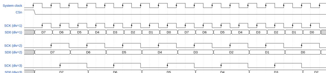
QMI uses DDR input/output registers to enable a resolution of one half system clock cycle for output signal generation and input sampling. This allows QMI to support odd clock divisors, including divide-by-one (SCK frequency equal to system clock frequency).
i NOTE
In practice, the maximum SCK frequency is constrained by the limits of the attached QSPI device, the signal integrity afforded by the PCB layout, and IO delays in the pads. See Section 12.14.3.4 .
12.14.3.1. Input sampling and RXDELAY
QMI samples input data on the rising edge of SCK ( Section 12.14.3 ). To introduce additional delay to the input delay register (helpful when the round trip delay is longer than half an SCK cycle), use MO_TIMING.RXDELAY / M1_TIMING.RXDELAY . RXDELAY counts delay in half system clock cycles, instead of SCK cycles.
12.14.3.2. Chip select timing
To save power, chip select is de-asserted after a transaction completes. To leave chip select asserted after a transaction, use MO_TIMING.COOLDOWN / M1_TIMING.COOLDOWN . This can reduce latency and increase bus throughput.
Chip select can be asserted one system clock cycle early via MO_TIMING.SELECT_SETUP / M1_TIMING.SELECT_SETUP . Some flash devices require this setting at very high SCK frequencies. Without this setting, QMI asserts chip select one half SCK period before the first rising edge of SCK. This is simultaneous with the assertion of the first data on SDx.
Chip select hold time can also be extended by up to 3 additional system clock cycles via MO_TIMING.SELECT_HOLD / M1_TIMING.SELECT_HOLD .
To enforce a maximum amount of time that chip select can remain asserted, use MO_TIMING.MAX_SELECT / M1_TIMING.MAX_SELECT . This is useful for PSRAM devices, which must issue internal DRAM refresh cycles when deselected.
To enforce a minimum amount of time that chip select can remain de-asserted, use MO_TIMING.MIN_DESELECT / M1_TIMING.MIN_DESELECT .
12.14.3.3. Double transfer rate (DTR)
Some QSPI memory devices transfer data on both edges of SCK. This feature, known as double transfer rate (DTR) , allows a lower SCK frequency for a given data transfer rate, reducing EM emissions and the energy cost of toggling the external clock. To enable DTR mode (per-window and per-direction), set the MO_RFMT.DTR / M1_RFMT.DTR flag (for reads) or MO_WFMT.DTR / M1_WFMT.DTR (for writes).
QMI implements DTR by halving the clock frequency whilst maintaining the data rate. To achieve this, QMI inverts alternate single transfer rate SCK clock periods, transforming a low-high-low-high sequence into a low-high-high-low sequence. When DTR is disabled, the QMI launches data on SCK falling edges and captures on rising edges. When DTR is enabled, the QMI launches data at the point half-way in between two SCK edges, and captures on each edge, as shown in Figure 138 .
Figure 138. DTR is implemented by halving the SCK frequency whilst maintaining data rate.
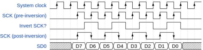
The diagram shows a system clock (blue) with a period of 1 unit. The SCK (pre-inversion) is a square wave with a period of 2 units. The 'Invert SCK?' signal is a square wave that is high for the first half and low for the second half of each SCK period. The SCK (post-inversion) is a square wave with a period of 2 units, inverted relative to the pre-inversion signal. The SD0 data is shown as a sequence of bits D7, D6, D5, D4, D3, D2, D1, D0, each occupying one SCK period.
Enabling DTR mode does not change the data timing, only the SCK timing. Data is launched at the point where a SCK negative edge would be, had the clock rate not been halved.
When DTR is enabled, the prefix and dummy phase of a transfer remain single transfer rate. In these phases, data bits are doubled to match the half-rate SCK , so that new data is ready in time for each rising edge only. Figure 139 shows the first byte (the command prefix) at single transfer rate and the second byte (address and data) at double transfer rate.
Figure 139. Parts of DTR-enabled transfers are still single transfer rate: effectively each data bit is sent twice.

The diagram shows a system clock (blue) with a period of 1 unit. The CSn signal is a square wave that is high for the first half and low for the second half of each SCK period. The SCK signal is a square wave with a period of 2 units. The SD0 data is shown as a sequence of bits D7, D6, D5, D4, D3, D2, D1, D0, each occupying one SCK period. The SD1 data is shown as a sequence of bits Q7, Q6, Q5, Q4, Q3, Q2, Q1, Q0, each occupying one SCK period. The first byte (Byte 0) is at single transfer rate (STR), and the second byte (Byte 1) is at double transfer rate (DTR).
The arrows on the SCK line in Figure 139 show the active edges of SCK (where data is captured). The single transfer rate portion of the access expects data capture on the rising edge. The double transfer rate portion of the access expects data capture on both edges.
Data travelling from device to host is likewise launched on both edges of SCK . Each time the QMI launches a new clock edge, there is some delay as transitions propagate through the RP2350 pad output delay, QSPI device SCK -to- SDx delay, and back in through the RP2350 SDx pad input delays. QMI captures data simultaneously with the launch of the next SCK edge, plus any delay configured by MO_TIMING .RXDELAY/ M1_TIMING .RXDELAY. The round-trip delay from SCK output back to SDx input provides the SDx input hold time. If the input setup time is not sufficient, you can increase RXDELAY . For more information, see the specific QSPI device datasheet, as well as Section 12.14.3.4.
12.14.3.4. AC timing parameters
The QMI interface is timed using the internal system clock. Skew between different QMI pins for inputs or outputs is kept to a minimum. Any additional setup or hold time is supported by using additional clock cycle delays as mentioned in other sections. Skew values vary depending on whether we consider just the dedicated QSPI pins ( QSPI_SS , QSPI_SD[3:0] , QSPI_SCLK ) or include the Bank 0 GPIO XIP special functions (for the additional QMI chip select). Different package options have different skew timing, shown below.
Table 1291. QMI Timing skew
| Interface | Typical Skew (ps) | Max Skew (ps) |
|---|---|---|
| QSPI input | 15 | 25 |
| QSPI output | 100 | 180 |
| Bank 0 GPIO (QFN-60) output | 1080 | 1725 |
| Bank 0 GPIO (QFN-80) output | 1280 | 2100 |
It is also useful to know the delay from internal register running on system clock to output pin, and similarly the delay from input pin to the sampling register running on system clock. Table 1292 provides worst case process, voltage, and temperature timings for inputs and outputs on QSPI, and outputs on GPIO. Note that this delay varies based on the VDDIO voltage level as shown in the table.
Table 1292. QMI Timing delay
| Path | Max delay (ns) VDDIO=3.3V | Max delay (ns) VDDIO=1.8V |
|---|---|---|
| QSPI input to system clock | 1.5 | 1.2 |
| system clock to QSPI output | 2.5 | 3.6 |
| Path | Max delay (ns) VDDIO=3.3V | Max delay (ns) VDDIO=1.8V |
|---|---|---|
| system clock to GPIO (QFN-60) output | 3.5 | 4.9 |
| system clock to GPIO (QFN-80) output | 4.1 | 5.4 |
12.14.4. Address translation
QMI applies a configurable mapping from the virtual address requested by the processor or DMA to the physical address transmitted to the external QSPI device. This is performed separately for each of the 16 MB chip select windows. You cannot map contents between devices.
Each window is divided into four panes , each independently mapped onto the physical address space for that window. The default configuration applied on QMI reset, as shown in Figure 140 , is a 1:1 identity mapping between virtual and physical addresses. In this state the address mapping has no effect, and the entire 16 MB address space of the external QSPI device is mapped directly into the system address space.
Figure 140. By default, each window is set up to map the full 16 MB virtual address space directly 1:1 with the 16 MB physical address space.
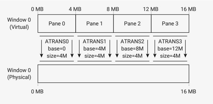
The diagram illustrates the default 1:1 identity mapping for Window 0. At the top, a horizontal axis represents the virtual address space from 0 MB to 16 MB, divided into four 4 MB panes: Pane 0, Pane 1, Pane 2, and Pane 3. Below each pane, an arrow points to a corresponding ATRANS register: ATRANS0 (base=0, size=4M), ATRANS1 (base=4M, size=4M), ATRANS2 (base=8M, size=4M), and ATRANS3 (base=12M, size=4M). At the bottom, a single block represents the physical address space, also from 0 MB to 16 MB, which is a direct 1:1 mapping of the virtual space above it.
Each pane corresponds to the one of the four ATTRANSx registers for that window: ATTRANS0 through ATTRANS3 for window 0, and ATTRANS4 through ATTRANS7 for window 1.
The virtual base address of each pane is fixed and assigned in 4 MB increments. There are two configurable parameters for the mapping of that pane into physical address space:
- • BASE : defines the physical address corresponding to offset 0 in the virtual address pane. Configured in units of 4 kB (one flash sector), ranging from 0 to (16 MB minus 4 kB).
- • SIZE : defines the amount of address space mapped by this pane. Configured in units of 4 kB (one flash sector) ranging from 0 to 4 MB.
The mapping grows from the start of the pane. A SIZE of 1 MB maps the first 1 MB of that pane’s virtual address range to downstream memory, and the remainder is unmapped. A SIZE of 0 means that no address within this virtual address pane is accessible. Accesses beyond the currently configured SIZE return a bus error, and do not pass through to the downstream QSPI bus. As a result, they have no effect on the external memory device.
Figure 141. The BASE of a pane defines where its physical mapping begins. The SIZE defines how far it extends. A SIZE of 0 means no addresses are mapped through that pane.
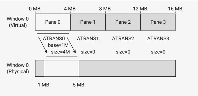
The diagram shows a non-identity mapping for Window 0. The virtual address space (0 MB to 16 MB) is divided into four 4 MB panes. ATRANS0 is configured with base=1M and size=4M, mapping the first 4 MB of virtual space to a physical address window from 1 MB to 5 MB. ATRANS1, ATRANS2, and ATRANS3 are all configured with size=0, meaning no addresses from those panes are mapped. The physical address space (0 MB to 16 MB) shows a shaded region from 1 MB to 5 MB, representing the mapped area, and the rest is unshaded.
Figure 141 shows an example mapping, where the first 4 MB of virtual address space for chip select 0 (virtual address offsets 0x000000 through 0x3fffff inclusive) map to a 4 MB physical address window starting at a 1 MB offset (physical address offsets 0x100000 through 0x4fffff inclusive). This mapping could be used for flash that contains a 1 MB
bootloader application followed by a 4 MB user application. Ideally, the user application should not be aware of the flash layout defined by the bootloader; that way, the same application can run under different bootloader implementations. The virtual-to-physical mapping solves this problem by making the storage location of the user application (starting at 1 MB) independent of the address it appears at in the system address space (starting at 0 MB).
12.14.4.1. Bootrom support for address translation
The bootrom can automatically configure address translation at boot time, so that a binary stored at some arbitrary location in physical flash storage can appear at a runtime flash address of 0.
This is done automatically when the booted image is inside of a flash partition (Section 5.1.2), and can be adjusted manually based on a rolling window delta specified in the
IMAGE_DEF
of the launched executable (Section 5.1.4).
The bootrom source code and bootrom documentation often refers to the QMI
ATRANS
mapping as "rolling windows", due to the modulo address wrapping on 16 MB boundaries — see Section 5.1.19.
12.14.4.2. Translation and the XIP cache
The QMI address translation is performed downstream of the system XIP cache (Section 4.4.1). Therefore, the XIP cache is a virtual cache with respect to this translation, because the address translation performed inside QMI is opaque to the XIP cache.
Consequently, changes to the QMI address translation necessitate a flush of the XIP cache. From the cache's point of view, the translation change has moved QMI memory contents around in the cache's downstream address space in a way that is incoherent with the cache contents, so a flush is required to restore coherence. At a minimum, any virtual address whose
ATRANSx
register (
ATRANS0
through
ATRANS7
) has been modified, and which may be allocated in the cache in either the clean or the dirty state, must be flushed. It may be simplest to flush the entire cache.
QMI's address mapping creates another hazard: the same physical address may map to multiple virtual addresses, and therefore may be allocated multiple times in the XIP cache. When you write to a physical address through a cached virtual address alias, the XIP cache does not propagate the change to other aliases. To avoid this issue, do not allow multiple aliases of the same writable physical address at the same instant. Aliasing read-only memory is usually safe. Aliases that exist at different points in time (for example, across an RTOS context switch boundary) can be kept coherent with appropriate cleaning and flushing when the translation is changed.
12.14.5. Direct mode
In direct mode, the AHB XIP address window is disconnected from the QSPI bus, and the bus is controlled through a TX/RX FIFO pair, similar to a normal SPI peripheral. In this state, the XIP window becomes inaccessible. Attempting to access it generates a bus fault. This mode is used for low-level access to the QSPI bus, for example when issuing flash erase/programming commands, or when accessing QSPI device status registers.
All direct-mode operation is controlled through
DIRECT_CSR
, with data being exchanged through
DIRECT_TX
and
DIRECT_RX
. To enable direct mode, first set
DIRECT_CSR.EN
, and then poll for
DIRECT_CSR.BUSY
to go low to ensure that any in-progress XIP transfer at the point direct mode was enabled has completed.
Direct mode has its own clock divisor and RX sampling delay, configured by
DIRECT_CSR.CLKDIV
and
DIRECT_CSR.RXDELAY
. These are separate from the per-window settings configured in
MO_TIMING/M1_TIMING
, because serial commands used for control purposes may have different frequency limits than data accesses used for execute-in-place.
For each push to
DIRECT_TX
, QMI will issue 8 or 16 bits of FIFO data to the QSPI bus. Optionally, the same number of bits are simultaneously sampled and returned in
DIRECT_RX
. The clock is initially low, and data is always captured on the rising edge of
SCK
, transitioning on the subsequent falling edge.
After pushing to
DIRECT_TX
,
DIRECT_CSR.BUSY
will go high, and remain high until all direct-mode activity has completed. This works even if no RX data is returned, so is more reliable than polling the RX FIFO status. The
BUSY
flag
stays high for half an SCK period after the transfer finishes, to ensure safe chip select timing when this is used to drive the chip selects — see Section 12.14.5.2 .
QMI will never push to a full RX FIFO, or drop data as a result of the FIFO being full — instead, the interface is paused until the system pops DIRECT_RX . This avoids a common trap of RX data being lost when the processor is heavily interrupted during direct-mode operation, but software must take care not to poll for DIRECT_CSR.BUSY low without also checking the RX FIFO, as this can cause a deadlock when the FIFO fills.
12.14.5.1. Controls in DIRECT_TX
The TX FIFO carries control information as well as data, with data in the 16 LSBs, and control information in the immediately more-significant bits:
- • DIRECT_TX.NOPUSH inhibits the DIRECT_RX push which would match this TX data. This avoids creating garbage when pushing control/address information at the start of a transfer.
- • DIRECT_TX.DWIDTH is the data width of this FIFO record. 0 means the 8 LSBs contain data, and 1 means the 16 LSBs contain data. This also determines the amount of data returned in the matching DIRECT_RX entry.
- • DIRECT_TX.IWIDTH is the interface width (single-dual/quad) used to clock out this FIFO record. The corresponding RX data is sampled at the same width.
- • DIRECT_TX.OE controls the pad direction for bidirectional transfers. It is ignored for serial IWIDTH , since SD0 is always an output and SD1 always an input. At dual/quad width, it must be set in order to enable the output drivers for the duration of this FIFO record. The TX data is don't-care when IWIDTH is dual/quad and OE is not set.
The default when all control bits are zero is an 8-bit serial transfer, with 8 bits of sampled data returned. Therefore, you can ignore the control bits and treat this as a plain 8-bit data FIFO.
12.14.5.2. Chip select control
There are two options for driving the chip selects, both via DIRECT_CSR :
- • DIRECT_CSR.ASSERT_CS0N and DIRECT_CSR.ASSERT_CS1N will immediately drive the corresponding chip select low when set
- • DIRECT_CSR.AUTO_CS0N and DIRECT_CSR.AUTO_CS1N configure the corresponding chip select to be set low whenever the interface is busy, i.e. when the DIRECT_CSR.BUSY flag is high due to a previous DIRECT_TX push
! IMPORTANT
The ASSERT_CSxN fields assert the chip select unconditionally , including when DIRECT_CSR.EN is clear. Software must take care not to set these fields when XIP transfers may be active.
12.14.6. List of registers
The QMI control registers start at address 0x400d0000 , defined as XIP_QMI_BASE in the SDK.
Table 1293. List of QMI registers
| Offset | Name | Info |
|---|---|---|
| 0x00 | DIRECT_CSR | Control and status for direct serial mode Direct serial mode allows the processor to send and receive raw serial frames, for programming, configuration and control of the external memory devices. Only SPI mode 0 (CPOL=0 CPHA=0) is supported. |
| 0x04 | DIRECT_TX | Transmit FIFO for direct mode |
| Offset 0x42fc8 0x42fcc 0x42fd0 0x42fd4 0x42fd8 | Name DEVID DEVTYPE PIDR4 PIDR5 PIDR6 | Info Device Configuration register Device Type Identifier register CoreSight Periperal ID4 CoreSight Periperal ID5 CoreSight Periperal ID6 |
|---|---|---|
| 0x08 | DIRECT_RX | Receive FIFO for direct mode |
| 0x0c | M0_TIMING | Timing configuration register for memory address window 0. |
| 0x10 | M0_RFMT | Read transfer format configuration for memory address window |
| 0x14 | M0_RCMD | Command constants used for reads from memory address window 0. |
| 0x18 | M0_WFMT | Write transfer format configuration for memory address window |
| 0x1c | M0_WCMD | Command constants used for writes to memory address window |
| 0x20 | M1_TIMING | Timing configuration register for memory address window 1. |
| 0x24 | M1_RFMT | Read transfer format configuration for memory address window |
| 0x28 | M1_RCMD | Command constants used for reads from memory address window 1. |
| 0x2c | M1_WFMT | Write transfer format configuration for memory address window |
| 0x30 | M1_WCMD | Command constants used for writes to memory address window |
| 0x34 | ATRANS0 | Configure address translation for XIP virtual addresses 0x000000 through 0x3fffff (a 4 MiB window starting at +0 MiB). |
| 0x38 | ATRANS1 | Configure address translation for XIP virtual addresses 0x400000 through 0x7fffff (a 4 MiB window starting at +4 MiB). |
| 0x3c | ATRANS2 | Configure address translation for XIP virtual addresses 0x800000 through 0xbfffff (a 4 MiB window starting at +8 MiB). |
| 0x40 | ATRANS3 | Configure address translation for XIP virtual addresses 0xc00000 through 0xffffff (a 4 MiB window starting at +12 MiB). |
| 0x44 | ATRANS4 | Configure address translation for XIP virtual addresses 0x1000000 through 0x13fffff (a 4 MiB window starting at +16 MiB). |
| 0x48 | ATRANS5 | Configure address translation for XIP virtual addresses 0x1400000 through 0x17fffff (a 4 MiB window starting at +20 MiB). |
| 0x4c | ATRANS6 | Configure address translation for XIP virtual addresses 0x1800000 through 0x1bfffff (a 4 MiB window starting at +24 MiB). |
| 0x50 | ATRANS7 | Configure address translation for XIP virtual addresses 0x1c00000 through 0x1ffffff (a 4 MiB window starting at +28 MiB). |
QMI: DIRECT_CSR Register
Offset: 0x00
DescriptionControl and status for direct serial mode
Direct serial mode allows the processor to send and receive raw serial frames, for programming, configuration and control of the external memory devices. Only SPI mode 0 (CPOL=0 CPHA=0) is supported.
Table 1294.
DIRECT_CSR Register
| Bits 31:0 Bits 31:0 Bits 31:28 | column_2 | Description Description Input value for GPIO0…31. Description QSPI_SD : Input value on QSPI SD0 (MOSI), SD1 (MISO), SD2 and SD3 pins | Type RO Type RO Type RO | Reset - Reset 0x00000000 Reset 0x0 |
|---|---|---|---|---|
| 21 | Reserved. | - | - | |
| 20:18 | RXLEVEL | : Current level of DIRECT_RX FIFO | RO | 0x0 |
| 17 | RXFULL | : When 1, the DIRECT_RX FIFO is currently full. The serial interface will when the DIRECT_TX FIFO is empty or the DIRECT_RX FIFO is full. | RO | 0x0 |
| 16 | RXEMPTY | : When 1, the DIRECT_RX FIFO is currently empty. If the processor attempts to read more data, the FIFO state is not affected, but the value returned to the processor is undefined. | RO | 0x0 |
| 15 | Reserved. | - | - | |
| 14:12 | TXLEVEL | : Current level of DIRECT_TX FIFO | RO | 0x0 |
| 11 | TXEMPTY | : When 1, the DIRECT_TX FIFO is currently empty. Unless the processor pushes more data, transmission will stop and BUSY will go low once the current 8-bit serial frame completes. | RO | 0x0 |
| 10 | TXFULL | : When 1, the DIRECT_TX FIFO is currently full. If the processor tries to write more data, that data will be ignored. | RO | 0x0 |
| 9:8 | Reserved. | - | - | |
| 7 | AUTO_CS1N | : When 1, automatically assert the CS1n chip select line whenever the BUSY flag is set. | RW | 0x0 |
| 6 | AUTO_CS0N | : When 1, automatically assert the CS0n chip select line whenever the BUSY flag is set. | RW | 0x0 |
| 5:4 | Reserved. | - | - | |
| 3 | ASSERT_CS1N | : When 1, assert (i.e. drive low) the CS1n chip select line. Note that this applies even when DIRECT_CSR_EN is 0. | RW | 0x0 |
| 2 | ASSERT_CS0N | : When 1, assert (i.e. drive low) the CS0n chip select line. Note that this applies even when DIRECT_CSR_EN is 0. | RW | 0x0 |
| Bits | Description | Type | Reset |
|---|---|---|---|
| 1 | BUSY: Direct mode busy flag. If 1, data is currently being shifted in/out (or would be if the interface were not stalled on the RX FIFO), and the chip select must not yet be deasserted. The busy flag will also be set to 1 if a memory-mapped transfer is still in progress when direct mode is enabled. Direct mode blocks new memory-mapped transfers, but can't halt a transfer that is already in progress. If there is a chance that memory-mapped transfers may be in progress, the busy flag should be polled for 0 before asserting the chip select. (In practice you will usually discover this timing condition through other means, because any subsequent memory-mapped transfers when direct mode is enabled will return bus errors, which are difficult to ignore.) | RO | 0x0 |
| 0 | EN: Enable direct mode. In direct mode, software controls the chip select lines, and can perform direct SPI transfers by pushing data to the DIRECT_TX FIFO, and popping the same amount of data from the DIRECT_RX FIFO. Memory-mapped accesses will generate bus errors when direct serial mode is enabled. | RW | 0x0 |
QMI: DIRECT_TX Register
Offset: 0x04
Description
Transmit FIFO for direct mode
Table 1295.
DIRECT_TX Register
| Bits | Description | Type | Reset |
|---|---|---|---|
| 31:21 | Reserved. | - | - |
| 20 | NOPUSH: Inhibit the RX FIFO push that would correspond to this TX FIFO entry. Useful to avoid garbage appearing in the RX FIFO when pushing the command at the beginning of a SPI transfer. | WF | 0x0 |
| 19 | OE: Output enable (active-high). For single width (SPI), this field is ignored, and SD0 is always set to output, with SD1 always set to input. For dual and quad width (DSPI/QSPI), this sets whether the relevant SDx pads are set to output whilst transferring this FIFO record. In this case the command/address should have OE set, and the data transfer should have OE set or clear depending on the direction of the transfer. | WF | 0x0 |
| 18 | DWIDTH: Data width. If 0, hardware will transmit the 8 LSBs of the DIRECT_TX DATA field, and return an 8-bit value in the 8 LSBs of DIRECT_RX. If 1, the full 16-bit width is used. 8-bit and 16-bit transfers can be mixed freely. | WF | 0x0 |
| 17:16 | IWIDTH: Configure whether this FIFO record is transferred with single/dual/quad interface width (0/1/2). Different widths can be mixed freely. | WF | 0x0 |
| Enumerated values: | |||
| 0x0 → S: Single width |
| Bits | Description | Type | Reset |
|---|---|---|---|
| 0x1 → D: Dual width | |||
| 0x2 → Q: Quad width | |||
| 15:0 | DATA:
Data pushed here will be clocked out falling edges of SCK (or before the very first rising edge of SCK, if this is the first pulse). For each byte clocked out, the interface will simultaneously sample one byte, on rising edges of SCK, and push this to the DIRECT_RX FIFO. For 16-bit data, the least-significant byte is transmitted first. | WF | 0x0000 |
QMI: DIRECT_RX Register
Offset: 0x08
Description
Receive FIFO for direct mode
Table 1296.
DIRECT_RX Register
| Bits | Description | Type | Reset |
|---|---|---|---|
| 31:16 | Reserved. | - | - |
| 15:0 | With each byte clocked out on the serial interface, one byte will simultaneously be clocked in, and will appear in this FIFO. The serial interface will stall when this FIFO is full, to avoid dropping data. When 16-bit data is pushed into the TX FIFO, the corresponding RX FIFO push will also contain 16 bits of data. The least-significant byte is the first one received. | RF | 0x0000 |
QMI: M0_TIMING, M1_TIMING Registers
Offsets: 0x0c, 0x20
Description
Timing configuration register for memory address window 0/1.
Table 1297.
M0_TIMING,
M1_TIMING Registers
| Bits | Description | Type | Reset |
|---|---|---|---|
| 31:30 | COOLDOWN:
Chip select cooldown period. When a memory transfer finishes, the chip select remains asserted for 64 x COOLDOWN system clock cycles, plus half an SCK clock period (rounded up for odd SCK divisors). After this cooldown expires, the chip select is always deasserted to save power. If the next memory access arrives within the cooldown period, the QMI may be able to append more SCK cycles to the currently ongoing SPI transfer, rather than starting a new transfer. This reduces access latency and increases bus throughput. Specifically, the next access must be in the same direction (read/write), access the same memory window (chip select 0/1), and follow sequentially the address of the last transfer. If any of these are false, the new access will first deassert the chip select, then begin a new transfer. If COOLDOWN is 0, the address alignment configured by PAGEBREAK has been reached, or the total chip select assertion limit MAX_SELECT has been reached, the cooldown period is skipped, and the chip select will always be deasserted one half SCK period after the transfer finishes. | RW | 0x1 |
| Bits | Description | Type | Reset |
|---|---|---|---|
| 29:28 | PAGEBREAK: When page break is enabled, chip select will automatically deassert when crossing certain power-of-2-aligned address boundaries. The next access will always begin a new read/write SPI burst, even if the address of the next access follows in sequence with the last access before the page boundary. Some flash and PSRAM devices forbid crossing page boundaries with a single read/write transfer, or restrict the operating frequency for transfers that do cross page a boundary. This option allows the QMI to safely support those devices. This field has no effect when COOLDOWN is disabled. | RW | 0x0 |
| Enumerated values: | |||
| 0x0 → NONE: No page boundary is enforced | |||
| 0x1 → 256: Break bursts crossing a 256-byte page boundary | |||
| 0x2 → 1024: Break bursts crossing a 1024-byte quad-page boundary | |||
| 0x3 → 4096: Break bursts crossing a 4096-byte sector boundary | |||
| 27:26 | Reserved. | - | - |
| 25 | SELECT_SETUP: Add up to one additional system clock cycle of setup between chip select assertion and the first rising edge of SCK. The default setup time is one half SCK period, which is usually sufficient except for very high SCK frequencies with some flash devices. | RW | 0x0 |
| 24:23 | SELECT_HOLD: Add up to three additional system clock cycles of active hold between the last falling edge of SCK and the deassertion of this window's chip select. The default hold time is one system clock cycle. Note that flash datasheets usually give chip select active hold time from the last rising edge of SCK, and so even zero hold from the last falling edge would be safe. Note that this is a minimum hold time guaranteed by the QMI: the actual chip select active hold may be slightly longer for read transfers with low clock divisors and/or high sample delays. Specifically, if the point two cycles after the last RX data sample is later than the last SCK falling edge, then the hold time is measured from this point. Note also that, in case the final SCK pulse is masked to save energy (true for non-DTR reads when COOLDOWN is disabled or PAGE_BREAK is reached), all of QMI's timing logic behaves as though the clock pulse were still present. The SELECT_HOLD time is applied from the point where the last SCK falling edge would be if the clock pulse were not masked. | RW | 0x0 |
| Bits | Description | Type | Reset |
|---|---|---|---|
| 22:17 | MAX_SELECT: Enforce a maximum assertion duration for this window's chip select, in units of 64 system clock cycles. If 0, the QMI is permitted to keep the chip select asserted indefinitely when servicing sequential memory accesses (see COOLDOWN). This feature is required to meet timing constraints of PSRAM devices, which specify a maximum chip select assertion so they can perform DRAM refresh cycles. See also MIN_DESELECT, which can enforce a minimum deselect time. If a memory access is in progress at the time MAX_SELECT is reached, the QMI will wait for the access to complete before deasserting the chip select. This additional time must be accounted for to calculate a safe MAX_SELECT value. In the worst case, this may be a fully-formed serial transfer, including command prefix and address, with a data payload as large as one cache line. | RW | 0x00 |
| 16:12 | MIN_DESELECT: After this window's chip select is deasserted, it remains deasserted for half an SCK cycle (rounded up to an integer number of system clock cycles), plus MIN_DESELECT additional system clock cycles, before the QMI reasserts either chip select pin. Nonzero values may be required for PSRAM devices which enforce a longer minimum CS deselect time, so that they can perform internal DRAM refresh cycles whilst deselected. | RW | 0x00 |
| 11 | Reserved. | - | - |
| 10:8 | RXDELAY: Delay the read data sample timing, in units of one half of a system clock cycle. (Not necessarily half of an SCK cycle.) An RXDELAY of 0 means the sample is captured at the SDI input registers simultaneously with the rising edge of SCK launched from the SCK output register. At higher SCK frequencies, RXDELAY may need to be increased to account for the round trip delay of the pads, and the clock-to-Q delay of the QSPI memory device. | RW | 0x0 |
| 7:0 | CLKDIV: Clock divisor. Odd and even divisors are supported. Defines the SCK clock period in units of 1 system clock cycle. Divisors 1..255 are encoded directly, and a divisor of 256 is encoded with a value of CLKDIV=0. The clock divisor can be changed on-the-fly, even when the QMI is currently accessing memory in this address window. All other parameters must only be changed when the QMI is idle. If software is increasing CLKDIV in anticipation of an increase in the system clock frequency, a dummy access to either memory window (and appropriate processor barriers/fences) must be inserted after the Mx_TIMING write to ensure the SCK divisor change is in effect before the system clock is changed. | RW | 0x04 |
QMI: M0_RFMT, M1_RFMT Registers
Offsets: 0x10, 0x24
Description
Read transfer format configuration for memory address window 0/1.
Configure the bus width of each transfer phase individually, and configure the length or presence of the command prefix, command suffix and dummy/turnaround transfer phases. Only 24-bit addresses are supported.
The reset value of the Mx_RFMT register is configured to support a basic 03h serial read transfer with no additional configuration.
Table 1298.
M0_RFMT, M1_RFMT
Registers
| Bits | Description | Type | Reset |
|---|---|---|---|
| 31:29 | Reserved. | - | - |
| 28 | DTR : Enable double transfer rate (DTR) for read commands: address, suffix and read data phases are active on both edges of SCK. SDO data is launched centre-aligned on each SCK edge, and SDI data is captured on the SCK edge that follows its launch. DTR is implemented by halving the clock rate; SCK has a period of 2 x CLK_DIV throughout the transfer. The prefix and dummy phases are still single transfer rate. If the suffix is quad-width, it must be 0 or 8 bits in length, to ensure an even number of SCK edges. | RW | 0x0 |
| 27:19 | Reserved. | - | - |
| 18:16 | DUMMY_LEN : Length of dummy phase between command suffix and data phase, in units of 4 bits. (i.e. 1 cycle for quad width, 2 for dual, 4 for single) | RW | 0x0 |
| Enumerated values: | |||
| 0x0 → NONE: No dummy phase | |||
| 0x1 → 4: 4 dummy bits | |||
| 0x2 → 8: 8 dummy bits | |||
| 0x3 → 12: 12 dummy bits | |||
| 0x4 → 16: 16 dummy bits | |||
| 0x5 → 20: 20 dummy bits | |||
| 0x6 → 24: 24 dummy bits | |||
| 0x7 → 28: 28 dummy bits | |||
| 15:14 | SUFFIX_LEN : Length of post-address command suffix, in units of 4 bits. (i.e. 1 cycle for quad width, 2 for dual, 4 for single) Only values of 0 and 8 bits are supported. | RW | 0x0 |
| Enumerated values: | |||
| 0x0 → NONE: No suffix | |||
| 0x2 → 8: 8-bit suffix | |||
| 13 | Reserved. | - | - |
| 12 | PREFIX_LEN : Length of command prefix, in units of 8 bits. (i.e. 2 cycles for quad width, 4 for dual, 8 for single) | RW | 0x1 |
| Enumerated values: | |||
| 0x0 → NONE: No prefix | |||
| 0x1 → 8: 8-bit prefix | |||
| 11:10 | Reserved. | - | - |
| 9:8 | DATA_WIDTH : The width used for the data transfer | RW | 0x0 |
| Bits | Description | Type | Reset |
|---|---|---|---|
| Enumerated values: | |||
| 0x0 → S: Single width | |||
| 0x1 → D: Dual width | |||
| 0x2 → Q: Quad width | |||
| 7:6 | DUMMY_WIDTH
: The width used for the dummy phase, if any. If width is single, SD0/MOSI is held asserted low during the dummy phase, and SD1...SD3 are tristated. If width is dual/quad, all IOs are tristated during the dummy phase. | RW | 0x0 |
| Enumerated values: | |||
| 0x0 → S: Single width | |||
| 0x1 → D: Dual width | |||
| 0x2 → Q: Quad width | |||
| 5:4 | SUFFIX_WIDTH : The width used for the post-address command suffix, if any | RW | 0x0 |
| Enumerated values: | |||
| 0x0 → S: Single width | |||
| 0x1 → D: Dual width | |||
| 0x2 → Q: Quad width | |||
| 3:2 | ADDR_WIDTH : The transfer width used for the address. The address phase always transfers 24 bits in total. | RW | 0x0 |
| Enumerated values: | |||
| 0x0 → S: Single width | |||
| 0x1 → D: Dual width | |||
| 0x2 → Q: Quad width | |||
| 1:0 | PREFIX_WIDTH : The transfer width used for the command prefix, if any | RW | 0x0 |
| Enumerated values: | |||
| 0x0 → S: Single width | |||
| 0x1 → D: Dual width | |||
| 0x2 → Q: Quad width |
QMI: M0_RCMD, M1_RCMD Registers
Offsets: 0x14, 0x28
Description
Command constants used for reads from memory address window 0/1.
The reset value of the Mx_RCMD register is configured to support a basic 03h serial read transfer with no additional configuration.
Table 1299.
M0_RCMD, M1_RCMD
Registers
| Bits | Description | Type | Reset |
|---|---|---|---|
| 31:16 | Reserved. | - | - |
| Bits | Description | Type | Reset |
|---|---|---|---|
| 15:8 | SUFFIX: The command suffix bits following the address, if Mx_RFMT_SUFFIX_LEN is nonzero. | RW | 0xa0 |
| 7:0 | PREFIX: The command prefix bits to prepend on each new transfer, if Mx_RFMT_PREFIX_LEN is nonzero. | RW | 0x03 |
QMI: M0_WFMT, M1_WFMT Registers
Offsets: 0x18, 0x2c
Description
Write transfer format configuration for memory address window 0/1.
Configure the bus width of each transfer phase individually, and configure the length or presence of the command prefix, command suffix and dummy/turnaround transfer phases. Only 24-bit addresses are supported.
The reset value of the Mx_WFMT register is configured to support a basic 02h serial write transfer. However, writes to this window must first be enabled via the XIP_CTRL_WRITABLE_Mx bit for this window, as XIP memory is read-only by default.
Table 1300.
M0_WFMT, M1_WFMT
Registers
| Bits | Description | Type | Reset |
|---|---|---|---|
| 31:29 | Reserved. | - | - |
| 28 | DTR: Enable double transfer rate (DTR) for write commands: address, suffix and write data phases are active on both edges of SCK. SDO data is launched centre-aligned on each SCK edge, and SDI data is captured on the SCK edge that follows its launch. DTR is implemented by halving the clock rate; SCK has a period of 2 x CLK_DIV throughout the transfer. The prefix and dummy phases are still single transfer rate. If the suffix is quad-width, it must be 0 or 8 bits in length, to ensure an even number of SCK edges. | RW | 0x0 |
| 27:19 | Reserved. | - | - |
| 18:16 | DUMMY_LEN: Length of dummy phase between command suffix and data phase, in units of 4 bits. (i.e. 1 cycle for quad width, 2 for dual, 4 for single) | RW | 0x0 |
| Enumerated values: | |||
| 0x0 → NONE: No dummy phase | |||
| 0x1 → 4: 4 dummy bits | |||
| 0x2 → 8: 8 dummy bits | |||
| 0x3 → 12: 12 dummy bits | |||
| 0x4 → 16: 16 dummy bits | |||
| 0x5 → 20: 20 dummy bits | |||
| 0x6 → 24: 24 dummy bits | |||
| 0x7 → 28: 28 dummy bits | |||
| 15:14 | SUFFIX_LEN: Length of post-address command suffix, in units of 4 bits. (i.e. 1 cycle for quad width, 2 for dual, 4 for single) Only values of 0 and 8 bits are supported. | RW | 0x0 |
| Bits | Description | Type | Reset |
|---|---|---|---|
| Enumerated values: | |||
| 0x0 → NONE: No suffix | |||
| 0x2 → 8: 8-bit suffix | |||
| 13 | Reserved. | - | - |
| 12 | PREFIX_LEN : Length of command prefix, in units of 8 bits. (i.e. 2 cycles for quad width, 4 for dual, 8 for single) | RW | 0x1 |
| Enumerated values: | |||
| 0x0 → NONE: No prefix | |||
| 0x1 → 8: 8-bit prefix | |||
| 11:10 | Reserved. | - | - |
| 9:8 | DATA_WIDTH : The width used for the data transfer | RW | 0x0 |
| Enumerated values: | |||
| 0x0 → S: Single width | |||
| 0x1 → D: Dual width | |||
| 0x2 → Q: Quad width | |||
| 7:6 | DUMMY_WIDTH
: The width used for the dummy phase, if any. If width is single, SD0/MOSI is held asserted low during the dummy phase, and SD1...SD3 are tristated. If width is dual/quad, all IOs are tristated during the dummy phase. | RW | 0x0 |
| Enumerated values: | |||
| 0x0 → S: Single width | |||
| 0x1 → D: Dual width | |||
| 0x2 → Q: Quad width | |||
| 5:4 | SUFFIX_WIDTH : The width used for the post-address command suffix, if any | RW | 0x0 |
| Enumerated values: | |||
| 0x0 → S: Single width | |||
| 0x1 → D: Dual width | |||
| 0x2 → Q: Quad width | |||
| 3:2 | ADDR_WIDTH : The transfer width used for the address. The address phase always transfers 24 bits in total. | RW | 0x0 |
| Enumerated values: | |||
| 0x0 → S: Single width | |||
| 0x1 → D: Dual width | |||
| 0x2 → Q: Quad width | |||
| 1:0 | PREFIX_WIDTH : The transfer width used for the command prefix, if any | RW | 0x0 |
| Enumerated values: | |||
| 0x0 → S: Single width |
| Bits | Description | Type | Reset |
|---|---|---|---|
| 0x1 → D: Dual width | |||
| 0x2 → Q: Quad width |
QMI: M0_WCMD, M1_WCMD Registers
Offsets: 0x1c, 0x30
Description
Command constants used for writes to memory address window 0/1.
The reset value of the Mx_WCMD register is configured to support a basic 02h serial write transfer with no additional configuration.
Table 1301.
M0_WCMD,
M1_WCMD Registers
| Bits | Description | Type | Reset |
|---|---|---|---|
| 31:16 | Reserved. | - | - |
| 15:8 | SUFFIX: The command suffix bits following the address, if Mx_WFMT_SUFFIX_LEN is nonzero. | RW | 0xa0 |
| 7:0 | PREFIX: The command prefix bits to prepend on each new transfer, if Mx_WFMT_PREFIX_LEN is nonzero. | RW | 0x02 |
QMI: ATRANS0, ATRANS4 Registers
Offsets: 0x34, 0x44
Description
Configure address translation for a 4 MiB window of XIP virtual addresses starting at \( n \times 4 \) MiB.
Address translation allows a program image to be executed in place at multiple physical flash addresses (for example, a double-buffered flash image for over-the-air updates), without the overhead of position-independent code.
At reset, the address translation registers are initialised to an identity mapping, so that they can be ignored if address translation is not required.
Note that the XIP cache is fully virtually addressed, so a cache flush is required after changing the address translation.
Table 1302. ATRANS0,
ATrans4 Registers
| Bits | Description | Type | Reset |
|---|---|---|---|
| 31:27 | Reserved. | - | - |
| 26:16 | SIZE:
Translation aperture size for this virtual address range, in units of 4 kiB (one flash sector). Bits 21:12 of the virtual address are compared to SIZE. Offsets greater than SIZE return a bus error, and do not cause a QSPI access. | RW | 0x400 |
| 15:12 | Reserved. | - | - |
| 11:0 | BASE:
Physical address base for this virtual address range, in units of 4 kiB (one flash sector). Taking a 24-bit virtual address, firstly bits 23:22 (the two MSBs) are masked to zero, and then BASE is added to bits 23:12 (the upper 12 bits) to form the physical address. Translation wraps on a 16 MiB boundary. | RW | 0x000 |
QMI: ATRANS1, ATRANS5 Registers
Offsets: 0x38, 0x48
Description
Configure address translation for XIP virtual addresses 0x400000 through 0x7fffff (a 4 MiB window starting at +4 MiB).
Address translation allows a program image to be executed in place at multiple physical flash addresses (for example, a double-buffered flash image for over-the-air updates), without the overhead of position-independent code.
At reset, the address translation registers are initialised to an identity mapping, so that they can be ignored if address translation is not required.
Note that the XIP cache is fully virtually addressed, so a cache flush is required after changing the address translation.
Table 1303. ATRANS1, ATRANS5 Registers
| Bits | Description | Type | Reset |
|---|---|---|---|
| 31:27 | Reserved. | - | - |
| 26:16 | SIZE:
Translation aperture size for this virtual address range, in units of 4 kiB (one flash sector). Bits 21:12 of the virtual address are compared to SIZE. Offsets greater than SIZE return a bus error, and do not cause a QSPI access. | RW | 0x400 |
| 15:12 | Reserved. | - | - |
| 11:0 | BASE:
Physical address base for this virtual address range, in units of 4 kiB (one flash sector). Taking a 24-bit virtual address, firstly bits 23:22 (the two MSBs) are masked to zero, and then BASE is added to bits 23:12 (the upper 12 bits) to form the physical address. Translation wraps on a 16 MiB boundary. | RW | 0x400 |
QMI: ATRANS2, ATRANS6 Registers
Offsets: 0x3c, 0x4c
Description
Configure address translation for XIP virtual addresses 0x800000 through 0xbfffff (a 4 MiB window starting at +8 MiB).
Address translation allows a program image to be executed in place at multiple physical flash addresses (for example, a double-buffered flash image for over-the-air updates), without the overhead of position-independent code.
At reset, the address translation registers are initialised to an identity mapping, so that they can be ignored if address translation is not required.
Note that the XIP cache is fully virtually addressed, so a cache flush is required after changing the address translation.
Table 1304. ATRANS2, ATRANS6 Registers
| Bits | Description | Type | Reset |
|---|---|---|---|
| 31:27 | Reserved. | - | - |
| 26:16 | SIZE:
Translation aperture size for this virtual address range, in units of 4 kiB (one flash sector). Bits 21:12 of the virtual address are compared to SIZE. Offsets greater than SIZE return a bus error, and do not cause a QSPI access. | RW | 0x400 |
| 15:12 | Reserved. | - | - |
| Bits | Description | Type | Reset |
|---|---|---|---|
| 11:0 | BASE:
Physical address base for this virtual address range, in units of 4 kiB (one flash sector). Taking a 24-bit virtual address, firstly bits 23:22 (the two MSBs) are masked to zero, and then BASE is added to bits 23:12 (the upper 12 bits) to form the physical address. Translation wraps on a 16 MiB boundary. | RW | 0x800 |
QMI: ATRANS3, ATRANS7 Registers
Offsets: 0x40, 0x50
Description
Configure address translation for XIP virtual addresses 0xc00000 through 0xffffffff (a 4 MiB window starting at +12 MiB).
Address translation allows a program image to be executed in place at multiple physical flash addresses (for example, a double-buffered flash image for over-the-air updates), without the overhead of position-independent code.
At reset, the address translation registers are initialised to an identity mapping, so that they can be ignored if address translation is not required.
Note that the XIP cache is fully virtually addressed, so a cache flush is required after changing the address translation.
Table 1305. ATRANS3, ATRANS7 Registers
| Bits | Description | Type | Reset |
|---|---|---|---|
| 31:27 | Reserved. | - | - |
| 26:16 | SIZE:
Translation aperture size for this virtual address range, in units of 4 kiB (one flash sector). Bits 21:12 of the virtual address are compared to SIZE. Offsets greater than SIZE return a bus error, and do not cause a QSPI access. | RW | 0x400 |
| 15:12 | Reserved. | - | - |
| 11:0 | BASE:
Physical address base for this virtual address range, in units of 4 kiB (one flash sector). Taking a 24-bit virtual address, firstly bits 23:22 (the two MSBs) are masked to zero, and then BASE is added to bits 23:12 (the upper 12 bits) to form the physical address. Translation wraps on a 16 MiB boundary. | RW | 0xc00 |
12.15. System Control Registers
These registers are not associated with any particular peripheral. They control, or provide information about, system-level hardware such as the bus fabric. This is also where chip identification information such as the JEDEC IDCODE is provided in a software-accessible manner.
12.15.1. SYSINFO
12.15.1.1. Overview
The sysinfo block contains system information. The first register contains the Chip ID, which allows the programmer to know which version of the chip software is running on. The second register indicates which package configuration is
used (QFN-60 or QFN-80). The third register will always read as 1.
12.15.1.2. List of registers
The sysinfo registers start at a base address of 0x40000000 (defined as
SYSINFO_BASE
in SDK).
Table 1306. List of SYSINFO registers
| Offset | Name | Info |
|---|---|---|
| 0x00 | CHIP_ID | JEDEC JEP-106 compliant chip identifier. |
| 0x04 | PACKAGE_SEL | Package selection indicator, 0 = QFN80, 1 = QFN60 |
| 0x08 | PLATFORM | Platform register. Allows software to know what environment it is running in during pre-production development. Post-production, the PLATFORM is always ASIC, non-SIM. |
| 0x14 | GITREF_RP2350 | Git hash of the chip source. Used to identify chip version. |
SYSINFO: CHIP_ID Register
Offset: 0x00
Description
JEDEC JEP-106 compliant chip identifier.
Table 1307. CHIP_ID Register
| Bits | Description | Type | Reset |
|---|---|---|---|
| 31:28 | REVISION | RO | - |
| 27:12 | PART | RO | - |
| 11:1 | MANUFACTURER | RO | - |
| 0 | STOP_BIT | RO | 0x1 |
SYSINFO: PACKAGE_SEL Register
Offset: 0x04
Table 1308. PACKAGE_SEL Register
| Bits | Description | Type | Reset |
|---|---|---|---|
| 31:1 | Reserved. | - | - |
| 0 | Package selection indicator, 0 = QFN80, 1 = QFN60 | RO | 0x0 |
SYSINFO: PLATFORM Register
Offset: 0x08
Description
Platform register. Allows software to know what environment it is running in during pre-production development. Post-production, the PLATFORM is always ASIC, non-SIM.
Table 1309. PLATFORM Register
| Bits | Description | Type | Reset |
|---|---|---|---|
| 31:5 | Reserved. | - | - |
| 4 | GATESIM | RO | - |
| 3 | BATCHSIM | RO | - |
| 2 | HDLSIM | RO | - |
| 1 | ASIC | RO | - |
| Bits | Description | Type | Reset |
|---|---|---|---|
| 0 | FPGA | RO | - |
SYSINFO: GITREF_RP2350 Register
Offset: 0x14
Table 1310.
GITREF_RP2350
Register
| Bits | Description | Type | Reset |
|---|---|---|---|
| 31:0 | Git hash of the chip source. Used to identify chip version. | RO | - |
12.15.2. SYSCFG
12.15.2.1. Overview
The system config block controls miscellaneous chip settings, including:
- • Check debug halt status of both cores
- • Processor GPIO input synchroniser control (set to 1 to allow input synchroniser bypassing to reduce latency for synchronous clocks)
- • SWD interface control from inside the chip (allows one core to debug another, which may make debug connectivity easier)
- • State-retaining memory power down (SRAM periphery can be powered down when not in use to save a small amount of power)
- ◦ when powered down in this way, power is still applied to the SRAM storage array; use the Power Manager (Chapter 6) to completely remove power
- • Additional controls found in the AUXCTRL register
12.15.2.2. Changes from RP2040
- • Moved the NMI mask to per-core registers in the EPPB (Section 3.7.5.1). The new registers reset on a processor warm reset, which avoids issues with NMIs asserting during the bootrom early boot process.
- • Expanded MEMPOWERDOWN to cover new memory banks
- • Removed controls from DBGFORCE to account for the new single-DP debug topology
12.15.2.3. List of registers
The system config registers start at a base address of 0x40008000 (defined as SYSCFG_BASE in SDK).
Table 1311. List of
SYSCFG registers
| Offset | Name | Info |
|---|---|---|
| 0x00 | PROC_CONFIG | Configuration for processors |
Table 1313.
PROC_IN_SYNC_BYPA
SS Register
| Bits | Description | Type | Reset |
|---|---|---|---|
| 31:0 | GPIO | RW | 0x00000000 |
SYSCFG: PROC_IN_SYNC_BYPASS_HI Register
Offset: 0x08
Description
For each bit, if 1, bypass the input synchronizer between that GPIO and the GPIO input register in the SIO. The input synchronizers should generally be unbypassed, to avoid injecting metastabilities into processors. If you're feeling brave, you can bypass to save two cycles of input latency. This register applies to GPIO 32...47. USB GPIO 56..57 QSPI GPIO 58..63
Table 1314.
PROC_IN_SYNC_BYPA
SS_HI Register
| Bits | Description | Type | Reset |
|---|---|---|---|
| 31:28 | QSPI_SD | RW | 0x0 |
| 27 | QSPI_CSN | RW | 0x0 |
| 26 | QSPI_SCK | RW | 0x0 |
| 25 | USB_DM | RW | 0x0 |
| 24 | USB_DP | RW | 0x0 |
| 23:16 | Reserved. | - | - |
| 15:0 | GPIO | RW | 0x0000 |
SYSCFG: DBGFORCE Register
Offset: 0x0c
Description
Directly control the chip SWD debug port
Table 1315.
DBGFORCE Register
| Bits | Description | Type | Reset |
|---|---|---|---|
| 31:4 | Reserved. | - | - |
| 3 | ATTACH: Attach chip debug port to syscfg controls, and disconnect it from external SWD pads. | RW | 0x0 |
| 2 | SWCLK: Directly drive SWCLK, if ATTACH is set | RW | 0x1 |
| 1 | SWDI: Directly drive SWDIO input, if ATTACH is set | RW | 0x1 |
| 0 | SWDO: Observe the value of SWDIO output. | RO | - |
SYSCFG: MEMPOWERDOWN Register
Offset: 0x10
Description
Control PD pins to memories.
Set high to put memories to a low power state. In this state the memories will retain contents but not be accessible
Use with caution
Table 1316.
MEMPOWERDOWN
Register
| Bits | Description | Type | Reset |
|---|---|---|---|
| 31:13 | Reserved. | - | - |
| 12 | BOOTRAM | RW | 0x0 |
| Bits | Description | Type | Reset |
|---|---|---|---|
| 11 | ROM | RW | 0x0 |
| 10 | USB | RW | 0x0 |
| 9 | SRAM9 | RW | 0x0 |
| 8 | SRAM8 | RW | 0x0 |
| 7 | SRAM7 | RW | 0x0 |
| 6 | SRAM6 | RW | 0x0 |
| 5 | SRAM5 | RW | 0x0 |
| 4 | SRAM4 | RW | 0x0 |
| 3 | SRAM3 | RW | 0x0 |
| 2 | SRAM2 | RW | 0x0 |
| 1 | SRAM1 | RW | 0x0 |
| 0 | SRAM0 | RW | 0x0 |
SYSCFG: AUXCTRL Register
Offset: 0x14
Description
Auxiliary system control register
Table 1317. AUXCTRL Register
| Bits | Description | Type | Reset |
|---|---|---|---|
| 31:8 | Reserved. | - | - |
| 7:0 | * Bits 7:3: Reserved * Bit 2: Set to mask OTP power analogue power supply detection from resetting OTP controller and PSM * Bit 1: When clear, the LPOSC output is XORed into the TRNG ROSC output as an additional, uncorrelated entropy source. When set, this behaviour is disabled. * Bit 0: Force POWMAN clock to switch to LPOSC, by asserting its WDRESET input. This must be set before initiating a watchdog reset of the RSM from a stage that includes CLOCKS, if POWMAN is running from clk_ref at the point that the watchdog reset takes place. Otherwise, the short pulse generated on clk_ref by the reset of the CLOCKS block may affect POWMAN register state. | RW | 0x00 |
12.15.3. TBMAN
TBMAN refers to the testbench manager, used during chip development simulations to verify the design. During these simulations TBMAN allows software running on RP2350 to control the testbench and simulation environment. On the real chip, it has no effect other than providing a single PLATFORM register that indicates that this is the real chip. This PLATFORM functionality is duplicated in the sysinfo (Section 12.15.1) registers.
12.15.3.1. List of registers
The TBMAN registers start at a base address of
0x40160000
(defined as
TBMAN_BASE
in SDK).
Table 1318. List of TBMAN registers
| Offset | Name | Info |
|---|---|---|
| 0x0 | PLATFORM | Indicates the type of platform in use |
TBMAN: PLATFORM Register
Offset: 0x0
Description
Indicates the type of platform in use
Table 1319. PLATFORM Register
| Bits | Description | Type | Reset |
|---|---|---|---|
| 31:3 | Reserved. | - | - |
| 2 | HDLSIM: Indicates the platform is a simulation | RO | 0x0 |
| 1 | FPGA: Indicates the platform is an FPGA | RO | 0x0 |
| 0 | ASIC: Indicates the platform is an ASIC | RO | 0x1 |
12.15.4. BUSCTRL
This block provides basic controls and monitoring for the system bus fabric.
12.15.4.1. Bus priority
RP2350 implements a dynamic bus priority scheme described in
Section 2.1.1
. The
BUS_PRIORITY
register implements the priority controls for this scheme.
12.15.4.2. Performance counters
There are four 24-bit counters, each of which can subscribe to a single performance event from the system bus fabric. Counters saturate at a value of all-ones: the counter stops incrementing when it reaches its maximum value, rather than wrapping to zero.
The performance counters are initially disabled: you must write
1
to
PERFCTR_EN
before the counters begin to increment. Write any value to a counter to clear the counter to zero in before running a profiled section of code, and enable the counters immediately before entering the profiled section. Disable the counters again immediately upon leaving the profiled section. The counters do not support arbitrary writes: they only count up from zero.
Write to a performance event selector register
PERFSEL0
through
PERFSEL3
to select the performance event which increments the corresponding counter,
PERFCTR0
through
PERFCTR3
.
For each of the seventeen downstream bus ports on the main system AHB5 crossbar shown in Figure 5 , there are four types of event which the performance counters detect. These events do not distinguish reads from writes, but they do distinguish different types of bus stall, which can be helpful when diagnosing performance issues. The types of event are:
Access
Increment when any access completes on this downstream port.
Contested access
Increment when any access completes on this downstream port which previously stalled due to the port being
occupied by another access. For example, if two managers access an initially idle port simultaneously, one will complete before the other. The access that completes first is said to not be contested, and does not increment this counter. The access that completes second (which was initially deferred due to the access from the other manager) is contested, and increments this counter when it completes.
Upstream-stalled cycle
Increment once per cycle while any manager experiences a stall on this port. This may be either due to arbitration with another manager (a contested access) or due to a stall on the downstream bus port, such as access to a slow peripheral. This is measured at the port , before leaving the main AHB5 crossbar.
Downstream-stalled cycle
Increment once per cycle while this port itself experiences a stall on the downstream bus. This indicates the peripheral or memory device itself being slow to respond, such as an XIP cache miss.
The first two event types listed above are the same as RP2040. The latter two are new for RP2350.
12.15.4.3. List of registers
The Bus Fabric registers start at a base address of 0x40068000 (defined as BUSCTRL_BASE in SDK).
Table 1320. List of BUSCTRL registers
| Offset | Name | Info |
|---|---|---|
| 0x00 | BUS_PRIORITY | Set the priority of each master for bus arbitration. |
| 0x04 | BUS_PRIORITY_ACK | Bus priority acknowledge |
| 0x08 | PERFCTR_EN | Enable the performance counters. If 0, the performance counters do not increment. This can be used to precisely start/stop event sampling around the profiled section of code. The performance counters are initially disabled, to save energy. |
| 0x0c | PERFCTR0 | Bus fabric performance counter 0 |
| 0x10 | PERFSEL0 | Bus fabric performance event select for PERFCTR0 |
| 0x14 | PERFCTR1 | Bus fabric performance counter 1 |
| 0x18 | PERFSEL1 | Bus fabric performance event select for PERFCTR1 |
| 0x1c | PERFCTR2 | Bus fabric performance counter 2 |
| 0x20 | PERFSEL2 | Bus fabric performance event select for PERFCTR2 |
| 0x24 | PERFCTR3 | Bus fabric performance counter 3 |
| 0x28 | PERFSEL3 | Bus fabric performance event select for PERFCTR3 |
BUSCTRL: BUS_PRIORITY Register
Offset: 0x00
Description
Set the priority of each master for bus arbitration.
Table 1321. BUS_PRIORITY Register
| Bits | Description | Type | Reset |
|---|---|---|---|
| 31:13 | Reserved. | - | - |
| 12 | DMA_W: 0 - low priority, 1 - high priority | RW | 0x0 |
| 11:9 | Reserved. | - | - |
| 8 | DMA_R: 0 - low priority, 1 - high priority | RW | 0x0 |
| Bits | Description | Type | Reset |
|---|---|---|---|
| 7:5 | Reserved. | - | - |
| 4 | PROC1 : 0 - low priority, 1 - high priority | RW | 0x0 |
| 3:1 | Reserved. | - | - |
| 0 | PROC0 : 0 - low priority, 1 - high priority | RW | 0x0 |
BUSCTRL: BUS_PRIORITY_ACK Register
Offset: 0x04
Description
Bus priority acknowledge
Table 1322.
BUS_PRIORITY_ACK
Register
| Bits | Description | Type | Reset |
|---|---|---|---|
| 31:1 | Reserved. | - | - |
| 0 | Goes to 1 once all arbiters have registered the new global priority levels. Arbiters update their local priority when servicing a new nonsequential access. In normal circumstances this will happen almost immediately. | RO | 0x0 |
BUSCTRL: PERFCTR_EN Register
Offset: 0x08
Table 1323.
PERFCTR_EN Register
| Bits | Description | Type | Reset |
|---|---|---|---|
| 31:1 | Reserved. | - | - |
| 0 | Enable the performance counters. If 0, the performance counters do not increment. This can be used to precisely start/stop event sampling around the profiled section of code. The performance counters are initially disabled, to save energy. | RW | 0x0 |
BUSCTRL: PERFCTR0 Register
Offset: 0x0c
Description
Bus fabric performance counter 0
Table 1324.
PERFCTR0 Register
| Bits | Description | Type | Reset |
|---|---|---|---|
| 31:24 | Reserved. | - | - |
| 23:0 | Busfabric saturating performance counter 0 Count some event signal from the busfabric arbiters, if PERFCTR_EN is set. Write any value to clear. Select an event to count using PERFSEL0 | WC | 0x000000 |
BUSCTRL: PERFSEL0 Register
Offset: 0x10
Description
Bus fabric performance event select for PERFCTR0
Table 1325. PERFSEL0 Register
| Bits | Description | Type | Reset |
|---|---|---|---|
| 31:7 | Reserved. | - | - |
| 6:0 | Select an event for PERFCTR0. For each downstream port of the main crossbar, four events are available: ACCESS, an access took place; ACCESS_CONTESTED, an access took place that previously stalled due to contention from other masters; STALL_DOWNSTREAM, count cycles where any master stalled due to a stall on the downstream bus; STALL_UPSTREAM, count cycles where any master stalled for any reason, including contention from other masters. | RW | 0x1f |
| Enumerated values: | |||
| 0x00 → SIOB_PROC1_STALL_UPSTREAM | |||
| 0x01 → SIOB_PROC1_STALL_DOWNSTREAM | |||
| 0x02 → SIOB_PROC1_ACCESS_CONTESTED | |||
| 0x03 → SIOB_PROC1_ACCESS | |||
| 0x04 → SIOB_PROC0_STALL_UPSTREAM | |||
| 0x05 → SIOB_PROC0_STALL_DOWNSTREAM | |||
| 0x06 → SIOB_PROC0_ACCESS_CONTESTED | |||
| 0x07 → SIOB_PROC0_ACCESS | |||
| 0x08 → APB_STALL_UPSTREAM | |||
| 0x09 → APB_STALL_DOWNSTREAM | |||
| 0x0a → APB_ACCESS_CONTESTED | |||
| 0x0b → APB_ACCESS | |||
| 0x0c → FASTPERI_STALL_UPSTREAM | |||
| 0x0d → FASTPERI_STALL_DOWNSTREAM | |||
| 0x0e → FASTPERI_ACCESS_CONTESTED | |||
| 0x0f → FASTPERI_ACCESS | |||
| 0x10 → SRAM9_STALL_UPSTREAM | |||
| 0x11 → SRAM9_STALL_DOWNSTREAM | |||
| 0x12 → SRAM9_ACCESS_CONTESTED | |||
| 0x13 → SRAM9_ACCESS | |||
| 0x14 → SRAM8_STALL_UPSTREAM | |||
| 0x15 → SRAM8_STALL_DOWNSTREAM | |||
| 0x16 → SRAM8_ACCESS_CONTESTED | |||
| 0x17 → SRAM8_ACCESS | |||
| 0x18 → SRAM7_STALL_UPSTREAM | |||
| 0x19 → SRAM7_STALL_DOWNSTREAM | |||
| 0x1a → SRAM7_ACCESS_CONTESTED | |||
| 0x1b → SRAM7_ACCESS | |||
| 0x1c → SRAM6_STALL_UPSTREAM |
| Bits | Description | Type | Reset |
|---|---|---|---|
| 0x1d → SRAM6_STALL_DOWNSTREAM | |||
| 0x1e → SRAM6_ACCESS_CONTESTED | |||
| 0x1f → SRAM6_ACCESS | |||
| 0x20 → SRAM5_STALL_UPSTREAM | |||
| 0x21 → SRAM5_STALL_DOWNSTREAM | |||
| 0x22 → SRAM5_ACCESS_CONTESTED | |||
| 0x23 → SRAM5_ACCESS | |||
| 0x24 → SRAM4_STALL_UPSTREAM | |||
| 0x25 → SRAM4_STALL_DOWNSTREAM | |||
| 0x26 → SRAM4_ACCESS_CONTESTED | |||
| 0x27 → SRAM4_ACCESS | |||
| 0x28 → SRAM3_STALL_UPSTREAM | |||
| 0x29 → SRAM3_STALL_DOWNSTREAM | |||
| 0x2a → SRAM3_ACCESS_CONTESTED | |||
| 0x2b → SRAM3_ACCESS | |||
| 0x2c → SRAM2_STALL_UPSTREAM | |||
| 0x2d → SRAM2_STALL_DOWNSTREAM | |||
| 0x2e → SRAM2_ACCESS_CONTESTED | |||
| 0x2f → SRAM2_ACCESS | |||
| 0x30 → SRAM1_STALL_UPSTREAM | |||
| 0x31 → SRAM1_STALL_DOWNSTREAM | |||
| 0x32 → SRAM1_ACCESS_CONTESTED | |||
| 0x33 → SRAM1_ACCESS | |||
| 0x34 → SRAM0_STALL_UPSTREAM | |||
| 0x35 → SRAM0_STALL_DOWNSTREAM | |||
| 0x36 → SRAM0_ACCESS_CONTESTED | |||
| 0x37 → SRAM0_ACCESS | |||
| 0x38 → XIP_MAIN1_STALL_UPSTREAM | |||
| 0x39 → XIP_MAIN1_STALL_DOWNSTREAM | |||
| 0x3a → XIP_MAIN1_ACCESS_CONTESTED | |||
| 0x3b → XIP_MAIN1_ACCESS | |||
| 0x3c → XIP_MAIN0_STALL_UPSTREAM | |||
| 0x3d → XIP_MAIN0_STALL_DOWNSTREAM | |||
| 0x3e → XIP_MAIN0_ACCESS_CONTESTED | |||
| 0x3f → XIP_MAIN0_ACCESS | |||
| 0x40 → ROM_STALL_UPSTREAM |
| Bits | Description | Type | Reset |
|---|---|---|---|
| 0x41 → ROM_STALL_DOWNSTREAM | |||
| 0x42 → ROM_ACCESS_CONTESTED | |||
| 0x43 → ROM_ACCESS |
BUSCTRL: PERFCTR1 Register
Offset: 0x14
Description
Bus fabric performance counter 1
Table 1326.
PERFCTR1 Register
| Bits | Description | Type | Reset |
|---|---|---|---|
| 31:24 | Reserved. | - | - |
| 23:0 | Busfabric saturating performance counter 1 Count some event signal from the busfabric arbiters, if PERFCTR_EN is set. Write any value to clear. Select an event to count using PERFSEL1 | WC | 0x000000 |
BUSCTRL: PERFSEL1 Register
Offset: 0x18
Description
Bus fabric performance event select for PERFCTR1
Table 1327. PERFSEL1
Register
| Bits | Description | Type | Reset |
|---|---|---|---|
| 31:7 | Reserved. | - | - |
| 6:0 | Select an event for PERFCTR1. For each downstream port of the main crossbar, four events are available: ACCESS, an access took place; ACCESS_CONTESTED, an access took place that previously stalled due to contention from other masters; STALL_DOWNSTREAM, count cycles where any master stalled due to a stall on the downstream bus; STALL_UPSTREAM, count cycles where any master stalled for any reason, including contention from other masters. | RW | 0x1f |
| Enumerated values: | |||
| 0x00 → SIOB_PROC1_STALL_UPSTREAM | |||
| 0x01 → SIOB_PROC1_STALL_DOWNSTREAM | |||
| 0x02 → SIOB_PROC1_ACCESS_CONTESTED | |||
| 0x03 → SIOB_PROC1_ACCESS | |||
| 0x04 → SIOB_PROC0_STALL_UPSTREAM | |||
| 0x05 → SIOB_PROC0_STALL_DOWNSTREAM | |||
| 0x06 → SIOB_PROC0_ACCESS_CONTESTED | |||
| 0x07 → SIOB_PROC0_ACCESS | |||
| 0x08 → APB_STALL_UPSTREAM | |||
| 0x09 → APB_STALL_DOWNSTREAM | |||
| 0x0a → APB_ACCESS_CONTESTED |
| Bits | Description | Type | Reset |
|---|---|---|---|
| 0x0b → APB_ACCESS | |||
| 0x0c → FASTPERI_STALL_UPSTREAM | |||
| 0x0d → FASTPERI_STALL_DOWNSTREAM | |||
| 0x0e → FASTPERI_ACCESS_CONTESTED | |||
| 0x0f → FASTPERI_ACCESS | |||
| 0x10 → SRAM9_STALL_UPSTREAM | |||
| 0x11 → SRAM9_STALL_DOWNSTREAM | |||
| 0x12 → SRAM9_ACCESS_CONTESTED | |||
| 0x13 → SRAM9_ACCESS | |||
| 0x14 → SRAM8_STALL_UPSTREAM | |||
| 0x15 → SRAM8_STALL_DOWNSTREAM | |||
| 0x16 → SRAM8_ACCESS_CONTESTED | |||
| 0x17 → SRAM8_ACCESS | |||
| 0x18 → SRAM7_STALL_UPSTREAM | |||
| 0x19 → SRAM7_STALL_DOWNSTREAM | |||
| 0x1a → SRAM7_ACCESS_CONTESTED | |||
| 0x1b → SRAM7_ACCESS | |||
| 0x1c → SRAM6_STALL_UPSTREAM | |||
| 0x1d → SRAM6_STALL_DOWNSTREAM | |||
| 0x1e → SRAM6_ACCESS_CONTESTED | |||
| 0x1f → SRAM6_ACCESS | |||
| 0x20 → SRAM5_STALL_UPSTREAM | |||
| 0x21 → SRAM5_STALL_DOWNSTREAM | |||
| 0x22 → SRAM5_ACCESS_CONTESTED | |||
| 0x23 → SRAM5_ACCESS | |||
| 0x24 → SRAM4_STALL_UPSTREAM | |||
| 0x25 → SRAM4_STALL_DOWNSTREAM | |||
| 0x26 → SRAM4_ACCESS_CONTESTED | |||
| 0x27 → SRAM4_ACCESS | |||
| 0x28 → SRAM3_STALL_UPSTREAM | |||
| 0x29 → SRAM3_STALL_DOWNSTREAM | |||
| 0x2a → SRAM3_ACCESS_CONTESTED | |||
| 0x2b → SRAM3_ACCESS | |||
| 0x2c → SRAM2_STALL_UPSTREAM | |||
| 0x2d → SRAM2_STALL_DOWNSTREAM | |||
| 0x2e → SRAM2_ACCESS_CONTESTED |
| Bits | Description | Type | Reset |
|---|---|---|---|
| 0x2f → SRAM2_ACCESS | |||
| 0x30 → SRAM1_STALL_UPSTREAM | |||
| 0x31 → SRAM1_STALL_DOWNSTREAM | |||
| 0x32 → SRAM1_ACCESS_CONTESTED | |||
| 0x33 → SRAM1_ACCESS | |||
| 0x34 → SRAM0_STALL_UPSTREAM | |||
| 0x35 → SRAM0_STALL_DOWNSTREAM | |||
| 0x36 → SRAM0_ACCESS_CONTESTED | |||
| 0x37 → SRAM0_ACCESS | |||
| 0x38 → XIP_MAIN1_STALL_UPSTREAM | |||
| 0x39 → XIP_MAIN1_STALL_DOWNSTREAM | |||
| 0x3a → XIP_MAIN1_ACCESS_CONTESTED | |||
| 0x3b → XIP_MAIN1_ACCESS | |||
| 0x3c → XIP_MAIN0_STALL_UPSTREAM | |||
| 0x3d → XIP_MAIN0_STALL_DOWNSTREAM | |||
| 0x3e → XIP_MAIN0_ACCESS_CONTESTED | |||
| 0x3f → XIP_MAIN0_ACCESS | |||
| 0x40 → ROM_STALL_UPSTREAM | |||
| 0x41 → ROM_STALL_DOWNSTREAM | |||
| 0x42 → ROM_ACCESS_CONTESTED | |||
| 0x43 → ROM_ACCESS |
BUSCTRL: PERFCTR2 Register
Offset: 0x1c
Description
Bus fabric performance counter 2
Table 1328.
PERFCTR2 Register
| Bits | Description | Type | Reset |
|---|---|---|---|
| 31:24 | Reserved. | - | - |
| 23:0 | Busfabric saturating performance counter 2 Count some event signal from the busfabric arbiters, if PERFCTR_EN is set. Write any value to clear. Select an event to count using PERFSEL2 | WC | 0x000000 |
BUSCTRL: PERFSEL2 Register
Offset: 0x20
Description
Bus fabric performance event select for PERFCTR2
Table 1329. PERFSEL2 Register
| Bits | Description | Type | Reset |
|---|---|---|---|
| 31:7 | Reserved. | - | - |
| 6:0 | Select an event for PERFCTR2. For each downstream port of the main crossbar, four events are available: ACCESS, an access took place; ACCESS_CONTESTED, an access took place that previously stalled due to contention from other masters; STALL_DOWNSTREAM, count cycles where any master stalled due to a stall on the downstream bus; STALL_UPSTREAM, count cycles where any master stalled for any reason, including contention from other masters. | RW | 0x1f |
| Enumerated values: | |||
| 0x00 → SIOB_PROC1_STALL_UPSTREAM | |||
| 0x01 → SIOB_PROC1_STALL_DOWNSTREAM | |||
| 0x02 → SIOB_PROC1_ACCESS_CONTESTED | |||
| 0x03 → SIOB_PROC1_ACCESS | |||
| 0x04 → SIOB_PROC0_STALL_UPSTREAM | |||
| 0x05 → SIOB_PROC0_STALL_DOWNSTREAM | |||
| 0x06 → SIOB_PROC0_ACCESS_CONTESTED | |||
| 0x07 → SIOB_PROC0_ACCESS | |||
| 0x08 → APB_STALL_UPSTREAM | |||
| 0x09 → APB_STALL_DOWNSTREAM | |||
| 0x0a → APB_ACCESS_CONTESTED | |||
| 0x0b → APB_ACCESS | |||
| 0x0c → FASTPERI_STALL_UPSTREAM | |||
| 0x0d → FASTPERI_STALL_DOWNSTREAM | |||
| 0x0e → FASTPERI_ACCESS_CONTESTED | |||
| 0x0f → FASTPERI_ACCESS | |||
| 0x10 → SRAM9_STALL_UPSTREAM | |||
| 0x11 → SRAM9_STALL_DOWNSTREAM | |||
| 0x12 → SRAM9_ACCESS_CONTESTED | |||
| 0x13 → SRAM9_ACCESS | |||
| 0x14 → SRAM8_STALL_UPSTREAM | |||
| 0x15 → SRAM8_STALL_DOWNSTREAM | |||
| 0x16 → SRAM8_ACCESS_CONTESTED | |||
| 0x17 → SRAM8_ACCESS | |||
| 0x18 → SRAM7_STALL_UPSTREAM | |||
| 0x19 → SRAM7_STALL_DOWNSTREAM | |||
| 0x1a → SRAM7_ACCESS_CONTESTED | |||
| 0x1b → SRAM7_ACCESS | |||
| 0x1c → SRAM6_STALL_UPSTREAM |
| Bits | Description | Type | Reset |
|---|---|---|---|
| 0x1d → SRAM6_STALL_DOWNSTREAM | |||
| 0x1e → SRAM6_ACCESS_CONTESTED | |||
| 0x1f → SRAM6_ACCESS | |||
| 0x20 → SRAM5_STALL_UPSTREAM | |||
| 0x21 → SRAM5_STALL_DOWNSTREAM | |||
| 0x22 → SRAM5_ACCESS_CONTESTED | |||
| 0x23 → SRAM5_ACCESS | |||
| 0x24 → SRAM4_STALL_UPSTREAM | |||
| 0x25 → SRAM4_STALL_DOWNSTREAM | |||
| 0x26 → SRAM4_ACCESS_CONTESTED | |||
| 0x27 → SRAM4_ACCESS | |||
| 0x28 → SRAM3_STALL_UPSTREAM | |||
| 0x29 → SRAM3_STALL_DOWNSTREAM | |||
| 0x2a → SRAM3_ACCESS_CONTESTED | |||
| 0x2b → SRAM3_ACCESS | |||
| 0x2c → SRAM2_STALL_UPSTREAM | |||
| 0x2d → SRAM2_STALL_DOWNSTREAM | |||
| 0x2e → SRAM2_ACCESS_CONTESTED | |||
| 0x2f → SRAM2_ACCESS | |||
| 0x30 → SRAM1_STALL_UPSTREAM | |||
| 0x31 → SRAM1_STALL_DOWNSTREAM | |||
| 0x32 → SRAM1_ACCESS_CONTESTED | |||
| 0x33 → SRAM1_ACCESS | |||
| 0x34 → SRAM0_STALL_UPSTREAM | |||
| 0x35 → SRAM0_STALL_DOWNSTREAM | |||
| 0x36 → SRAM0_ACCESS_CONTESTED | |||
| 0x37 → SRAM0_ACCESS | |||
| 0x38 → XIP_MAIN1_STALL_UPSTREAM | |||
| 0x39 → XIP_MAIN1_STALL_DOWNSTREAM | |||
| 0x3a → XIP_MAIN1_ACCESS_CONTESTED | |||
| 0x3b → XIP_MAIN1_ACCESS | |||
| 0x3c → XIP_MAIN0_STALL_UPSTREAM | |||
| 0x3d → XIP_MAIN0_STALL_DOWNSTREAM | |||
| 0x3e → XIP_MAIN0_ACCESS_CONTESTED | |||
| 0x3f → XIP_MAIN0_ACCESS | |||
| 0x40 → ROM_STALL_UPSTREAM |
| Bits | Description | Type | Reset |
|---|---|---|---|
| 0x41 → ROM_STALL_DOWNSTREAM | |||
| 0x42 → ROM_ACCESS_CONTESTED | |||
| 0x43 → ROM_ACCESS |
BUSCTRL: PERFCTR3 Register
Offset: 0x24
Description
Bus fabric performance counter 3
Table 1330.
PERFCTR3 Register
| Bits | Description | Type | Reset |
|---|---|---|---|
| 31:24 | Reserved. | - | - |
| 23:0 | Busfabric saturating performance counter 3 Count some event signal from the busfabric arbiters, if PERFCTR_EN is set. Write any value to clear. Select an event to count using PERFSEL3 | WC | 0x000000 |
BUSCTRL: PERFSEL3 Register
Offset: 0x28
Description
Bus fabric performance event select for PERFCTR3
Table 1331. PERFSEL3
Register
| Bits | Description | Type | Reset |
|---|---|---|---|
| 31:7 | Reserved. | - | - |
| 6:0 | Select an event for PERFCTR3. For each downstream port of the main crossbar, four events are available: ACCESS, an access took place; ACCESS_CONTESTED, an access took place that previously stalled due to contention from other masters; STALL_DOWNSTREAM, count cycles where any master stalled due to a stall on the downstream bus; STALL_UPSTREAM, count cycles where any master stalled for any reason, including contention from other masters. | RW | 0x1f |
| Enumerated values: | |||
| 0x00 → SIOB_PROC1_STALL_UPSTREAM | |||
| 0x01 → SIOB_PROC1_STALL_DOWNSTREAM | |||
| 0x02 → SIOB_PROC1_ACCESS_CONTESTED | |||
| 0x03 → SIOB_PROC1_ACCESS | |||
| 0x04 → SIOB_PROC0_STALL_UPSTREAM | |||
| 0x05 → SIOB_PROC0_STALL_DOWNSTREAM | |||
| 0x06 → SIOB_PROC0_ACCESS_CONTESTED | |||
| 0x07 → SIOB_PROC0_ACCESS | |||
| 0x08 → APB_STALL_UPSTREAM | |||
| 0x09 → APB_STALL_DOWNSTREAM | |||
| 0x0a → APB_ACCESS_CONTESTED |
| Bits | Description | Type | Reset |
|---|---|---|---|
| 0x0b → APB_ACCESS | |||
| 0x0c → FASTPERI_STALL_UPSTREAM | |||
| 0x0d → FASTPERI_STALL_DOWNSTREAM | |||
| 0x0e → FASTPERI_ACCESS_CONTESTED | |||
| 0x0f → FASTPERI_ACCESS | |||
| 0x10 → SRAM9_STALL_UPSTREAM | |||
| 0x11 → SRAM9_STALL_DOWNSTREAM | |||
| 0x12 → SRAM9_ACCESS_CONTESTED | |||
| 0x13 → SRAM9_ACCESS | |||
| 0x14 → SRAM8_STALL_UPSTREAM | |||
| 0x15 → SRAM8_STALL_DOWNSTREAM | |||
| 0x16 → SRAM8_ACCESS_CONTESTED | |||
| 0x17 → SRAM8_ACCESS | |||
| 0x18 → SRAM7_STALL_UPSTREAM | |||
| 0x19 → SRAM7_STALL_DOWNSTREAM | |||
| 0x1a → SRAM7_ACCESS_CONTESTED | |||
| 0x1b → SRAM7_ACCESS | |||
| 0x1c → SRAM6_STALL_UPSTREAM | |||
| 0x1d → SRAM6_STALL_DOWNSTREAM | |||
| 0x1e → SRAM6_ACCESS_CONTESTED | |||
| 0x1f → SRAM6_ACCESS | |||
| 0x20 → SRAM5_STALL_UPSTREAM | |||
| 0x21 → SRAM5_STALL_DOWNSTREAM | |||
| 0x22 → SRAM5_ACCESS_CONTESTED | |||
| 0x23 → SRAM5_ACCESS | |||
| 0x24 → SRAM4_STALL_UPSTREAM | |||
| 0x25 → SRAM4_STALL_DOWNSTREAM | |||
| 0x26 → SRAM4_ACCESS_CONTESTED | |||
| 0x27 → SRAM4_ACCESS | |||
| 0x28 → SRAM3_STALL_UPSTREAM | |||
| 0x29 → SRAM3_STALL_DOWNSTREAM | |||
| 0x2a → SRAM3_ACCESS_CONTESTED | |||
| 0x2b → SRAM3_ACCESS | |||
| 0x2c → SRAM2_STALL_UPSTREAM | |||
| 0x2d → SRAM2_STALL_DOWNSTREAM | |||
| 0x2e → SRAM2_ACCESS_CONTESTED |
| Bits | Description | Type | Reset |
|---|---|---|---|
| 0x2f → SRAM2_ACCESS | |||
| 0x30 → SRAM1_STALL_UPSTREAM | |||
| 0x31 → SRAM1_STALL_DOWNSTREAM | |||
| 0x32 → SRAM1_ACCESS_CONTESTED | |||
| 0x33 → SRAM1_ACCESS | |||
| 0x34 → SRAM0_STALL_UPSTREAM | |||
| 0x35 → SRAM0_STALL_DOWNSTREAM | |||
| 0x36 → SRAM0_ACCESS_CONTESTED | |||
| 0x37 → SRAM0_ACCESS | |||
| 0x38 → XIP_MAIN1_STALL_UPSTREAM | |||
| 0x39 → XIP_MAIN1_STALL_DOWNSTREAM | |||
| 0x3a → XIP_MAIN1_ACCESS_CONTESTED | |||
| 0x3b → XIP_MAIN1_ACCESS | |||
| 0x3c → XIP_MAIN0_STALL_UPSTREAM | |||
| 0x3d → XIP_MAIN0_STALL_DOWNSTREAM | |||
| 0x3e → XIP_MAIN0_ACCESS_CONTESTED | |||
| 0x3f → XIP_MAIN0_ACCESS | |||
| 0x40 → ROM_STALL_UPSTREAM | |||
| 0x41 → ROM_STALL_DOWNSTREAM | |||
| 0x42 → ROM_ACCESS_CONTESTED | |||
| 0x43 → ROM_ACCESS |