13. OTP
RP2350 provides 8 kB of one-time programmable storage (OTP), which holds:
- • Preprogrammed per-device information, such as unique device identifier and oscillator trim values
- • Security configuration such as debug disable and secure boot enable
- • Public key fingerprints for secure boot
- • Symmetric keys for decryption of flash contents into SRAM
- • Configuration for the USB bootloader, such as customising VID/PID and descriptors
- • Bootable software images, for low-cost flashless applications or custom bootloaders
- • Any other user-defined data, such as per-device personalisation values
For the full listing of predefined OTP contents, see Section 13.10 .
OTP is physically an array of 4096 rows of 24 bits each. You can directly access these 24-bit values, but there is also hardware support for storing 16 bits of data in each row, with 6 bits of Hamming ECC protection and 2 bits of bit polarity reversal protection, yielding an ECC data capacity of 8192 bytes.
On a blank device, the OTP contents is all zeroes, except for some basic device information pre-programmed during manufacturing test. Each bit can be irreversibly programmed from zero to one. To program the OTP contents:
- • Directly access the registers using the SBPI bridge
- • Call the bootrom
otp_accessAPI ( Section 5.4.8.21 ) - • Use the PICOB00T interface of the USB bootloader ( Section 5.6 )
RP2350 enforces page-based permissions on OTP to partition Secure from Non-secure data and to ensure that contents that should not change do not change. The OTP address space is logically partitioned into 64 pages, each 64 rows in size, for a total of 128 bytes of ECC data per page. Pages initially have full read-write permissions, but can be restricted to read-only or inaccessible for each of Secure, Non-secure and bootloader access.
The page permissions themselves are stored in OTP. Locking pages in this way is an irreversible operation, referred to as
hard locking
. The hardware also supports
soft locking
, where a page's permissions are further restricted by writing to the relevant register in
SW_LOCK0
through
SW_LOCK63
; this restriction remains in effect until the next OTP reset. Resetting the OTP block also resets the processors, so soft locking can be used to restrict the availability of sensitive content like decryption keys to early boot stages.
OTP access keys ( Section 13.5.2 ) provide an additional layer of protection. A fixed challenge is written to a write-only OTP area. Pages registered to that key require the key to be entered to a write-only register in order to open read or write access. This supports configuration data that can be accessed or edited by the board manufacturer, but not by general firmware running on the device.
13.1. OTP address map
The OTP hardware resides in a 128 kB region starting at
0x40120000
(OTP_BASE in the SDK). Bit 16 of the address is used to select either the OTP control registers, in the lower 64 kB, or one of the OTP read data aliases, in the upper 64 kB of this space.
The OTP control registers ( Section 13.9 ) are aliased at 4 kB intervals to implement the usual set, clear, and XOR atomic write aliases described in Section 2.1.3 .
The read data region starting at
0x40130000
divides further into four aliases:
- •
0x40130000,OTP_DATA_BASE: ECC read alias. A 32-bit read returns the ECC-corrected data for two neighbouring rows, or all-ones on permission failure. Only the first 8 kB is populated.
- •
0x40138000,OTP_DATA_GUARDED_BASE: ECC guarded read alias. Successful reads return the same data asOTP_DATA_BASE. Only the first 8 kB is populated. - •
0x40134000,OTP_DATA_RAW_BASE: raw read alias. A 32-bit read directly returns the 24-bit contents of a single row, with zeroes in the eight MSBs, or returns all-ones on permission failure. - •
0x4013c000,OTP_DATA_RAW_GUARDED_BASE: raw, guarded read alias. Successful reads return the same data asOTP_DATA_RAW_BASE.
Bit 14 of the address selects ECC (0) vs raw (1). Bit 15 of the address selects unguarded (0) vs guarded (1) access. Guarded reads return the same data as unguarded reads, but perform additional hardware consistency checks and return bus faults on permission failure. For more information, see Section 13.1.1 .
! IMPORTANT
The read data regions starting at
0x40130000
are accessible only when
USR.DCTRL
is set, otherwise all reads return a bus error response. This bit is clear when the OTP is being programmed via the SBPI bridge.
Writing to the read data aliases is not a valid operation, and will always return a bus fault. The OTP is programmed by the SBPI bridge, which is used internally by the bootrom
otp_access
API,
Section 5.4.8.21
.
13.1.1. Guarded reads
Reads through the guarded aliases differ from unguarded reads in the following ways:
- • Permission failures return bus faults rather than a bit pattern of all-ones.
- • Uncorrectable ECC errors return a bus fault if detected.
- • Guarded reads perform an additional hardware consistency check to detect power transients. If this check fails, the read returns a bus fault.
These checks help to make the OTP fail-safe in contexts where deliberate fault injection is a possibility. For example, the RP2350 bootrom uses guarded reads to check boot configuration flags.
The data returned from a successful guarded read is the same as the data returned by a successful read from the corresponding unguarded alias.
! IMPORTANT
Users relying on OTP data in a Secure context should always perform guarded reads, and it is strongly recommended to use ECC. For rows where ECC is not possible, software should take care to ensure the consistency of data across multiple overlapping reads.
13.2. Background: OTP IP details
The RP2350 OTP subsystem uses the Synopsys NVM OTP IP, which comes in 3 parts:
- • Integrated Power Supply (IPS), including:
- ◦ Charge Pump (for programming)
- ◦ Regulator (for reading)
- • OTP Macro (SHF, Fuse)
- ◦ \( 4096 \times 24 \) (8 kB with ECC, 16-bit ECC write granularity)
- • Access port (AP), providing:
- ◦ Basic read access
- ◦ Programming access
- ◦ ECC and bit redundancy
- ◦ BOOT function, which polls for stable OTP power supply at start-of-day
13.3. Background: OTP hardware architecture
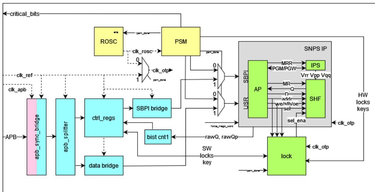
This diagram shows the integration of the three Synopsys IP components, and the Raspberry Pi hardware added to make this all function in the context of RP2350's system and security architecture. More specifically:
- • APB interface(s) to connect to the SoC
- • Internal ring oscillator with clock edge randomisation
- • Power-up state machine, running off the ring oscillator
- • Lock shim, sitting between the SNPS RTL and the memory core (fuse)
Figure 142. OTP architecture
The OTP subsystem clock is initially provided by the OTP boot oscillator (Section 13.3.3) during hardware startup, but switches to
clk_ref
before any software runs on the processors. The frequency of
clk_ref
must not exceed 25 MHz when accessing the OTP.
13.3.1. Lock shim
The lock shim is inserted between the Synopsys AP block and the SHF block, and is used to enforce read/write page locks, based on:
- • The OTP address presented on the AP → SHF bus
- • The read/write strobe on the AP → SHF bus
- • The security attribute of the upstream bus access which caused this SHF access (assumed to be Secure if SBPI is currently enabled via
USR.DCTRL)
Because the Synopsys AP performs both reads and writes in the course of programming an OTP row, it is impossible to disable reads to an address without also disabling writes. Three lock states are supported:
- • Read/Write
- • Read-only
- • Inaccessible
The full locking scheme is described in in Section 13.5 , but to summarise:
- • The lock state of each OTP page is read from OTP at boot time.
- • There is a separate copy of the lock state for Secure/Non-secure accesses. The lock shim applies the Secure read permissions to Secure reads, and the Non-secure read permissions to Non-secure reads. There is no such rule for writes, because Non-secure code is not capable of accessing the programming hardware.
- • The lock encoding in OTP storage is such that a page can always be locked down to a less permissive state (in the order RW → RO → Inaccessible) but can never return to a more permissive state.
- • Software can advance the state of each individual lock at runtime without programming OTP, and this lasts until the OTP PSM is re-run.
- • Software locks also obey the lock progression order (RW → RO → Inaccessible) and can not be regressed.
The full locking scheme is described in in Section 13.5 .
13.3.2. External interfaces
The OTP integration has one upstream APB interface, which splits internally onto two separate interfaces. This guarantees the hardware only serves a single upstream APB access at a time, with a single PPROT security level.
The first APB interface is the data interface (or data bridge) (OTPD). It has the following characteristics:
- • Read-only
- • Connects to the Synopsys device access port (DAP)
- • Data interface reads always return 32 or 24 bits of valid data
- • The data interface address is rounded down to a multiple of 32 bits, so that narrow reads return the correct byte lanes
- • There is an 8 kB window which supports 32-bit ECC reads
- ◦ Each upstream bus read is split into two OTP accesses, each of which returns 16 bits of error-corrected data from the OTP
- • There is an 8 kB window which supports guarded 32-bit ECC reads, and returns a bus error if the guarding read fails.
- ◦ Functions the same as the ECC read window, but reads the Synopsys boot word before accessing the OTP array, and return a bus error if the first read does not match the expected constant
- ◦ Used to increase confidence in software OTP reads in the bootrom
- • There is a 16 kB window which supports 24-bit raw reads
- ◦ Each access returns a single raw 24-bit OTP row, bypassing error correction
- ◦ Software must provide its own redundancy (e.g. triple majority vote)
- ◦ Allows bit-mutable data structures, such as boot flags, or thermometer counters
The second APB interface is the command interface. This provides two main functions:
- • Provides a bridge to the SBPI interface (Synopsys proprietary Serial and Byte-Parallel Interface bus)
- ◦ SBPI connects to the Programmable Master Controller (PMC), with access to the DAP, DATAPATH, charge pump (IPS), and fuse memory (SHF)
- ◦ Allows arbitrary OTP operations, including programming
- ◦ Only accessible to Secure reads and writes
- • Provides control registers for Raspberry Pi hardware
- ◦ Registers have different accessibility according to Secure/Non-secure and read/write
- ◦ Software lock registers are always readable by both security domains
Hardware configuration data read from OTP during the power-up sequence drives system-level control signals, e.g. disabling CoreSight APs. This is described in more detail in (Section 13.3.4).
A single system-level interrupt output (IRQ) generates interrupts for the following sources:
- • Secure read failed due to locks
- • Non-secure read failed due to locks
- • Write failed due to locks
- • SBPI FLAG, used by the PMC to signal completion
- • Data port access when DCTRL is set error
- ◦
USR.DCTRLtells the SNPS AP whether the SBPI bridge or data bridge can access the memory array; this help debugging SW if a data access is attempted whilst the DAP is inaccessible
- ◦
Any failed access also returns a bus fault (
PSLVERR
). To determine whether an OTP address is accessible, query the lock tables.
Non-secure code cannot access the interrupt status registers.
13.3.3. OTP boot oscillator
The OTP startup sequence (Section 13.3.4) runs from a local ring oscillator, dedicated to the OTP subsystem. This is separate from the system ring oscillator (the ROSC) which provides the system clock to run the processors during boot.
- • The OTP boot oscillator is the only clock used by the OTP power-up state machine
- • The OTP boot oscillator dynamically randomises its own frequency controls, to deliberately add jitter to the clock
- • The OTP boot oscillator stops when the PSM completes, and does not start again until the OTP resets
- • The OTP clock automatically switches to
clk_refwhen the OTP boot oscillator stops
The boot oscillator has a nominal frequency of 12MHz. It provides the clock for reading out hardware configuration from OTP, including the critical flags (Section 13.4) which configure hardware security features such as debug disable and the glitch detectors.
Keeping this oscillator local to the OTP hardware subsystem reduces the power signature of the clock itself, due to the lower switched clock capacitance. Along with the random jitter of the frequency controls, this helps frustrate attempts to recover OTP access keys and debug keys via power signature analysis attacks, or to disable security features by timing fault injection against the OTP clock.
Only the OTP boot oscillator enables the ROSC frequency randomisation feature by default: for later operations using the system ROSC (Section 8.3), you must explicitly enable this feature on that oscillator, by programming the ROSC control registers. The crystal oscillator (XOSC) does not support frequency randomisation.
13.3.4. Power-up state machine
The OTP is the second item in the switched core domain's Power-On State Machine (Section 7.4), after the processor cold reset. OTP does not release its
rst_done
, or enable any debug interface (including the factory test JTAG described in Section 10.10), until the OTP PSM reads out OTP-resident hardware configuration. The
rst_done
output to the system
PSM holds the rest of the system in reset until the OTP PSM completes, so that no software runs until the OTP's contents are known.
The OTP boot sequence runs from a local ring oscillator. This oscillator is dedicated to the OTP subsystem, and is separate from the main system ROSC used by the processors at boot. The sequence is:
- 1. First, the PSM runs the Synopsys boot instruction. This has the following steps:
- a. Wait for the power supply to return a 'good' value.
- b. Read consistency check location until hardware sees the correct value for 16 successive reads. Consistency checks use predefined words stored in mask ROM cells with similar analogue properties to OTP cells.
- 2. Read critical flags (non-ECC): each critical bit is redundant across 8 OTP rows, with three-of-eight vote for each flag.
- 3. Read hardware access keys via ECC read interface.
- 4. Read valid bits for hardware access keys, including the debug keys ( Section 3.5.9.2 )
- 5. Initialise page lock registers from the lock page via raw read interface.
- 6. Assert
rst_donesignal to the system power-on state machine - 7. The system reset sequence continues, starting with the system ROSC
RP2350 A3 adds correctness checks and robustness to the PSM. For more information about these additions, see RP2350-E16 .
13.4. Critical flags
Critical flags enable hardware security features which are fundamental to RP2350's secure boot implementation. The OTP power-up state machine reads critical flags very early in the system reset sequence, before any code runs on the processors.
Most critical flags are in the main Boot Configuration page, page 1. These are listed under CRIT1 in the OTP data listing. The exceptions are the Arm/RISC-V disable flags, which are in the Chip Info page, page 0. This page is made read-only during factory programming, so users can not write to the CRIT0 flags.
Critical flags define
0
as the unprogrammed value, and
1
as the programmed value. On a blank device, all of the
CRIT1
flags are
0
. The reset value specified below is the value assigned to the internal logic net between the OTP reset being applied and the OTP PSM completing. For example, the reset value of
1
for the debug disable flags implies that debug is not accessible whilst the OTP PSM is running, but may be available afterward, depending on the value read from OTP storage.
- •
ARM_DISABLE
(reset:
0): Force the ARCHSEL register to RISC-V, at higher priority than RISC-V disable flag, secure boot enable flag, or default boot architecture flag. - •
RISCV_DISABLE
(reset:
0): Force the ARCHSEL register to Arm, at higher priority than the default boot architecture flag. - •
SECURE_BOOT_ENABLE
(reset:
1): Enable boot signature checking in bootrom, disable factory JTAG, and force the ARCHSEL register to Arm, at higher priority than the default boot architecture flag. - •
SECURE_DEBUG_DISABLE
(reset:
1): Disable factory JTAG, block Secure accesses from Mem-APs, and block halt requests to Secure processors.- ◦ Prevents secure AP accesses by masking their
ap_secure_ensignals. - ◦ Prevents secure processor halting by masking the Cortex-M33's
SPIDENandNSPIDENsignals. - ◦ Secure debug can be re-enabled by a Secure register in the OTP block.
- ◦ Re-enable of Secure debug can be disabled by a Secure write-1-only lock register, also in the OTP block.
- ◦ Prevents secure AP accesses by masking their
- •
DEBUG_DISABLE
(reset:
1): Completely disable the Mem-APs, in addition to disabling everything disabled by the secure
debug disable flag.
- •
BOOT_ARCH
(reset: 0): set the reset value of the
ARCHSEL
register (0 → Arm, 1 → RISC-V) if it has not been forced by other critical flags.
- ◦ Not critical, but hardware-read.
- • GLITCH_DETECTOR_ENABLE (reset: 0): pass an enable signal to the glitch detectors so that they can be armed before any software runs.
- • GLITCH_DETECTOR_SENS (reset: 0): configure the initial sensitivity of the glitch detector circuits.
Critical flags are encoded with a three-of-eight vote across eight consecutive OTP rows. Each flag is redundantly programmed to the same bit position in eight consecutive rows. Hardware considers the flag to be set if the bit reads as 1 in at least three of these eight rows. The flag is considered clear if no more than two bits are observed to be set.
i NOTE
As of RP2350 A3 the ARM_DISABLE flag has no effect, removing a potential unlock path for debug on a secured RP2350. Additionally, the combination of RISCV_DISABLE=1 and BOOT_ARCH=1 is decoded to an invalid state and the chip will not boot.
JTAG disable is ignored only if the customer RMA flag ( Section 13.7 ) is set.
For further discussion of the effects of the critical flags, see:
- • Section 3.5.9.1 for the effects of the debug disable flags
- • Section 3.9 for the effects of the Arm/RISC-V architecture select flags
- • Section 10.9 for the effects of the glitch detector configuration flags
- • Section 10.1.1 for discussion of the bootrom secure boot support enabled by the SECURE_BOOT_ENABLE flag
13.5. Page locks
The OTP protection hardware logically segments OTP into 64 pages (0 through 63), each 128 bytes in size, or equivalently 64 OTP rows.
Each page has a set of lock registers which determine read and write access for that page from Secure and Non-secure code. The lock registers are preloaded from OTP at reset, and can then be advanced (i.e. made less permissive) by software. Lock registers themselves are always world-readable.
Pages 61 through 63 are not so neatly described by a single set of lock registers. These pages store lock initialisation metadata. For more details, see Section 13.5.4 . This section describes the more common case of a page protected by a set of page locks.
13.5.1. Lock progression
Due to hardware constraints ( Section 13.3.1 ), read and write restrictions are not orthogonal: it's impossible to disallow reads to an address without also disallowing writes. So, the progression of locking for a given page is:
- 0. Read/Write
- 1. Read-only
- 2. Inaccessible
Lock state only increases . This is enforced in two ways:
- • Due to the nature of OTP and the choice of encoding, you cannot lower the OTP values preloaded to the lock registers during boot.
- • The lock registers ignore writes of lower-than-current values.
Secure and Non-secure use separate lock values, which can advance independently of one another. There is no hardware distinction between Non-secure Read/Write and Non-secure Read-only, since Non-secure can not directly write to the OTP anyway. It is still worth encoding, because Secure software performing a write on Non-secure software's behalf can check and enforce the Non-secure write lock.
You can reprogram bits from any state to any higher state. Locks use a 2-bit thermometer code: the initial all-zeroes state is read-write, and locks are advanced by programming first bit 0, then bit 1.
Lock bits in OTP are triple-redundant with a majority vote. They can't be ECC-protected, because they may be mutated bit-by-bit over multiple programming operations.
The OTP-resident lock bits are write-protected by their own Secure lock level. The lock pages are always world-readable.
The Secure lock registers can be advanced by Secure code, and are world-readable.
The Non-secure lock registers can be advanced by Secure or Non-secure code, and are world-readable.
13.5.2. OTP access keys
Page 61 contains 128-bit keys. Each key has a valid bit : when set, the key becomes completely inaccessible to software. The keys are always read out into hidden registers by hardware during startup so that hardware can perform key comparisons without exposing the keys to software.
Pages can require specific keys for some page permissions. To unlock the page, the user writes their key to a write-only register in the OTP block. The page remains unlocked for as long as the correct key is present in this register. To re-lock the page, erase the active key by writing zeroes to the key register.
The per-page lock config specifies the following:
- • a read key index 1-7, or 0 if there is no read key
- • a write key index 1-7 or 0 if there is no write key
- • the no-key state : either Read-only or Inaccessible, state of the page when no registered key has been entered by software into the key register
The no-key state is encoded as follows:
- • 0 for Read-only (lock level 1)
- • 1 for Inaccessible (lock level 2).
 TIP
TIP
Key index 7 does not exist in the configuration. If you specify key index 7, it is guaranteed to never match.
The hardware determines the key lock level by comparing the entered key to the key config of the current page, as follows:
- 1. If no keys are registered, the key lock level is 0
- 2. Else if keys are registered and no matching key is entered, the key lock level is 2 or 1 depending on the "no-key state" config
- 3. Else if a write key is registered and present, the key lock level is 0
- 4. Else if a read key is registered and present, the key lock level is 1
Hardware compares the key lock level to the page's lock level for the current security domain (Secure/Non-secure) and takes whichever is higher . For example, if a page has been made Non-secure read-only, there is nothing a key can do to make it Non-secure writable.
There are six 128-bit access keys stored in the OTP. Keys 5 and 6 also function as the Secure debug access key and
Non-secure debug access key, respectively. See Section 3.5.9.2 for information on how the debug keys affect external debug access.
You might use OTP access keys if a bootloader contains OTP configuration that needs to be Secure-writable only to the board owner , not to general Secure software on the device.
13.5.3. Lock encoding in OTP
Page locks are encoded as a 16-bit value. This value is stored as a pair of triple-redundant bytes, each byte occupying a 24-bit OTP row.
The lock halfword is encoded as follows:
| Bits | Purpose |
|---|---|
| 2:0 | Write key index, or 0 if no write key |
| 5:3 | Read key index, or 0 if no read key |
| 6 | No-key state, 0=Read-only 1=Inaccessible |
| 7 | Reserved |
| 9:8 | Secure lock state (thermometer code 0 → 2) |
| 11:10 | Non-secure lock state (thermometer code 0 → 2) |
| 13:12 | PicoBoot lock state (thermometer code 0 → 2) or software-defined use if PicoBoot OTP is disabled |
| 15:12 | Reserved |
13.5.4. Special pages
The following pages require special case handling in their lock checks:
- • The lock word region itself (pages 62 and 63)
- ◦ Lock words are always world-readable
- ◦ Lock words are writable by Secure code if the lock word itself permits Secure writes
- ◦ Consequently, lock words 62 and 63 are considered "spare", since they do not protect pages 62 and 63; the page 63 lock word is repurposed for the RMA flag
- • The hardware access key page (page 61)
- ◦ Contains OTP access keys and debug access keys
- ◦ Each key also has a valid bit ( rbit )
- ◦ Page 61 (key page) has all of the usual protections from the page 61 lock word
- ◦ If a key's valid bit is set, that key is inaccessible; the converse is not necessarily true
Page 0, known as the chip info page , is not a special page. Raspberry Pi sets page 0 to read-only during factory test, after writing chip identification and calibration values.
13.5.5. Permissions of blank devices
Each RP2350 device has some information programmed during manufacturing test. At this time, a small number of hard page lock bits are also programmed:
- • Page 0, which contains chip information, is read-only for all accesses.
- • Pages 1 and 2, which contain boot config and boot key fingerprints, are read-only for Non-secure access, read-write for Secure access, and read-write for bootloader access.
- • Page 62, which contains only the page 62 lock word, is read-only for Non-secure access, read-write for Secure access, and read-write for bootloader access (as a partial workaround for RP2350-E28 ).
- • Page 63, which contains the RMA flag, is read-only for Non-secure and bootloader access, and read-write for Secure access.
This minimal set of default permissions on blank devices avoids certain classes of security model violation, like Non-secure code being able to brick the chip by overwriting the boot key fingerprints with invalid data. In this context, the term blank device refers to a device that has gone through manufacturing test programming, but has not had any other OTP bits programmed by the user.
You can add additional soft or hard locks to these default permissions, with the exception of page 0. Page 0 cannot be hard-locked, since the secure read-only permission prevents a user from altering its lock word.
Lock words 2 through 61, covering all pages with user-defined contents, are left unprogrammed. On a blank device, these pages are fully accessible from all domains. Before launching any Non-secure application, you should apply at least a soft read-only lock to all pages that are not explicitly allocated for Non-secure use. To do this, write to SW_LOCK2 through SW_LOCK61 . For devices that you don't expect to RMA, such as those that have passed board-level manufacturing tests, you should lock secure writes to the RMA flag.
13.6. Error Correction Code (ECC)
ECC-protected rows store data in the following structure, accessible through a raw alias:
- • Bits 23:22 : bit repair by polarity (BRP) flag
- • Bits 21:16 : modified Hamming ECC code
- • Bits 15:0 (the 16 LSBs): data
RP2350 stores the following error correction data in the 8 MSBs of each 24-bit row:
- • a 6-bit modified Hamming code ECC, providing single-error-correct and double-error-detect capabilities
- • 2 bits of bit repair by polarity (BRP), which supports inverting the entire row at programming time to repair a single set bit that should be clear
Writes first encode ECC, then BRP. Reads first decode BRP, then ECC. When reading through an ECC data alias (
Section 13.1
), hardware performs correction transparently. ECC programming operations (writes) automatically generate ECC bits when you use the bootrom
otp_access
API (
Section 5.4.8.21
).
ECC is not suitable for data that mutates one bit at a time, since the ECC value is derived from the entire 16-bit data value. When storing data without ECC, use another form of redundancy, such as 3-way majority vote.
13.6.1. Bit repair by polarity (BRP)
Bit repair by polarity (BRP) compensates for a single bit present at time of programming.
When programming a row, hardware or software first calculates a 24-bit target value consisting of:
Before programming, an OTP row should contain all zeros. However, sometimes OTP rows contain a single bit that is already set to 1 , either due to manufacturing flaws or previous programming. If a bit is already set ( 1 ) in an OTP row
before programming, BRP checks the status of the corresponding bit in the target value. BRP compensates for this single set bit in one of two ways, depending on the corresponding value in the target value:
- • If the bit is clear (0), BRP inverts the target row and writes two ones in bits 23:22.
- • If the bit is set (1), BRP does not invert the target row, leaving two zeroes in bits 23:22.
When you read an OTP value through an ECC alias (Section 13.1), BRP checks for two ones in bits 23:22. When both bits 23 and 22 are set, BRP inverts the entire row before passing it to the modified Hamming code stage.
BRP makes it possible to store any 22-bit value in a row that initially has at most one bit set, preserving the correction margin of the modified Hamming code. During manufacturing test, hardware scans the entire OTP array to ensure no rows contain more than one pre-set bit.
13.6.2. Modified Hamming ECC
ECC generates six parity bits based on the data value stored in bits 15:0 of an OTP row. When programming a row, ECC generates those six parity bits and includes them in the target value as bits 21:16. This code consists of:
- • A 5-bit Hamming code that identifies single-bit errors
- • An even parity bit which allows two-bit errors to be detected in the Hamming code and the original 16-bit data
When you read an OTP value through an ECC alias (Section 13.1), ECC recalculates the six parity bits based on the value read from the OTP row. Then, ECC XORs the original six parity bits with the newly-calculated parity bits. This generates 6 new bits:
- • the 5 LSBs are the syndrome , a unique bit pattern that corresponds to each possible bit flip in the data value
- • the MSB distinguishes between odd and even numbers of bit flips
If all 6 bits in this value are zero, ECC did not detect an error. If the MSB is 1, the syndrome should indicate a single-bit error. ECC flips the corresponding data bit to recover from the error. If the MSB is 0, but the syndrome contains a value other than 0, the ECC detected an unrecoverable multi-bit error.
You can calculate 5-bit Hamming codes and parity bits with the following C code (adapted from the RP2350 bootrom source):
uint32_t even_parity(uint32_t input) {
    uint32_t rc = 0;
    while (input) {
        rc ^= input & 1;
        input >>= 1;
    }
    return rc;
}

const uint32_t otp_ecc_parity_table[6] = {
    0b0000001010110101011011,
    0b000000011011001101101,
    0b000001100011110001110,
    0b0000000001111110000,
    0b0000011110000000000,
    0b01111111111111111111
};

uint32_t s_otp_calculate_ecc(uint16_t x) {
    uint32_t p = x;
    for (uint i = 0; i < 6; ++i) {
        p |= even_parity(p & otp_ecc_parity_table[i]) << (16 + i);
    }
    return p;
}
}
13.7. Device decommissioning (RMA)
Decommissioning refers to destroying a device's sensitive contents and restoring some test or debug functionality when a device reaches the end of its security lifecycle. The OTP hardware can't actually destroy user data without circumventing write protection in some way. Instead, decommissioning is implemented with the RMA flag , which modifies devices in the following ways:
- • re-enables factory test JTAG which is otherwise disabled by the secure boot critical flag
- • makes pages 3 through 61 inaccessible
The RMA flag doesn't change permissions for page 0 (manufacturing data), pages 1 and 2 (boot configuration), page 61 (OTP access keys), or pages 62 and 63 (locks).
The RMA flag is encoded in a spare bit of the page 63 lock word. This lock word would otherwise be unused, since page 63 is one of the lock pages; consequently, it is not protected by a lock word. Instead, each lock word protects itself.
Like all other lock words, the page 63 lock word is protected by its own locks, which means it can be hard- and soft-locked to prevent the RMA flag being set. Locking the RMA flag makes it impossible to re-enable the factory JTAG interface if any of
CRIT1.SECURE_BOOT_ENABLE
,
CRIT1.DEBUG_DISABLE
or
CRIT1.SECURE_DEBUG_DISABLE
is set. This makes it impossible for Raspberry Pi to re-test such devices if they are returned for fault analysis.
! IMPORTANT
Setting the RMA flag does not destroy OTP contents, it merely renders it inaccessible. The design intent is for this to be irreversible, but hardware is never perfect. This is something the user's threat model must account for when programming the RMA flag on devices with sensitive OTP contents – for example, by personalising per-device OTP secrets to avoid class breaks if an attacker is able to retrieve the keys.
13.8. Imaging Vulnerability
The RP2350 OTP is intended to store boot key fingerprints and boot decryption keys. The ability to protect encrypted contents in external flash storage depends on the ability to protect the OTP contents from unauthorised or external reads. The OTP uses antifuse bit cells, which store data as a charge, similar to a flash bit cell. They do not make use of a physical structural change as used in a traditional fuse cell. This makes them resistant to many imaging techniques, such as optical and scanning electron microscopy. However antifuse cells can be imaged using a novel technique called passive voltage contrast (PVC), using a focused ion beam (FIB) device.
PVC Whitepaper
For more information on passive voltage contrast imaging, read the whitepaper by IOActive:
https://www.ioactive.com/wp-content/uploads/2025/01/IOActive-RP2350HackingChallenge.pdf
This process involves decapsulating the die. Therefore physical access to the device is a strict requirement, and there is a moderate chance of destroying the die without being able to recover its OTP contents.
13.8.1. Best Practices
The following best practices minimise your susceptibility to imaging of OTP contents:
- • Provision unique keys per device, rather than sharing secrets across a fleet of devices.
- • Use chaff as described in the next section to make imaging more difficult.
13.8.2. Chaff
OTP bits come in pairs: two bits are stored in the isolated gates of two transistors, with a common bit line between them. This structure is known as a
bit cell
. In each 64-row OTP page, rows
i
and
\(
32 + i
\)
share the same bit cells. For example, the ECC halfwords
BOOTKEY0_0
and
BOOTKEY2_0
are physically colocated.
The particulars of the PVC technique make it difficult to distinguish which of the two bits in a bit cell is set. If one bit in each pair is known to be zero – for example, a key stored at the bottom of an otherwise blank page – then the data can be trivially read from the PVC image. However the presence of unknown data in both bits frustrates these attempts. This fact can be exploited by storing data redundantly in the top and bottom half of each page. Specifically:
- • Store arbitrary data in each row i from 0 to 31.
- • Store the 24-bit bitwise complement of those values in each row \( 32 + i \) .
The bitwise operations specified here are on the entire 24-bit raw row contents, including the ECC bit pattern.
An alternative technique is to store a random value in row
\(
32 + i
\)
and the XOR of that random value with the desired data value in row
i
. This is advantageous from a power side channel perspective because it avoids reading the secret value directly from OTP, and the example RP2350 encrypted bootloader uses a similar technique with a 4-way XOR. However the bitwise complement technique described above is recommended for pairwise chaff. This is the same as the XOR technique with a fixed XOR pattern of
0xfffff
.
13.9. List of registers
The OTP control registers start at a base address of
0x40120000
(defined as
OTP_BASE
in the SDK).
Table 1332. List of OTP registers
| Offset 0x42fc8 0x42fcc 0x42fd0 0x42fd4 0x42fd8 | Name DEVID DEVTYPE PIDR4 PIDR5 PIDR6 | Info Device Configuration register Device Type Identifier register CoreSight Periperal ID4 CoreSight Periperal ID5 CoreSight Periperal ID6 |
|---|---|---|
| them. This structure is known as a | bit cell . In each 64-row OTP page, rows i and 32 + i share the same bit cells. For | |
| example, the ECC halfwords | BOOTKEY0_0 and BOOTKEY2_0 are physically colocated. | |
| each pair is known to be zero — | for example, a key stored at the bottom of an otherwise blank page — then the data can | |
| • | Store arbitrary data in each row | i from 0 to 31. |
| • | Store the 24-bit bitwise complement of those values in each row 32 + i . | |
| An alternative technique is to store a random value in row | 32 + i and the XOR of that random value with the desired data | |
| value in row | i | . This is advantageous from a power side channel perspective because it avoids reading the secret value |
| 13.9. List of registers The OTP control registers start at a base address of | 0x40120000 (defined as OTP_BASE in the SDK). | |
| Offset OTP registers | Name | Info |
| 0x000 | SW_LOCK0 | Software lock register for page 0. |
| 0x004 | SW_LOCK1 | Software lock register for page 1. |
| 0x008 | SW_LOCK2 | Software lock register for page 2. |
| 0x00c | SW_LOCK3 | Software lock register for page 3. |
| 0x010 | SW_LOCK4 | Software lock register for page 4. |
| 0x014 | SW_LOCK5 | Software lock register for page 5. |
| 0x018 | SW_LOCK6 | Software lock register for page 6. |
| 0x01c | SW_LOCK7 | Software lock register for page 7. |
| 0x020 | SW_LOCK8 | Software lock register for page 8. |
| 0x024 | SW_LOCK9 | Software lock register for page 9. |
| 0x028 | SW_LOCK10 | Software lock register for page 10. |
| 0x02c | SW_LOCK11 | Software lock register for page 11. |
| 0x030 | SW_LOCK12 | Software lock register for page 12. |
| 0x034 | SW_LOCK13 | Software lock register for page 13. |
| 0x038 | SW_LOCK14 | Software lock register for page 14. |
| 0x03c | SW_LOCK15 | Software lock register for page 15. |
| 13.9. List of registers 13.9. List of registers | 1280 |
| Offset | Name | Info |
|---|---|---|
| 0x040 | SW_LOCK16 | Software lock register for page 16. |
| 0x044 | SW_LOCK17 | Software lock register for page 17. |
| 0x048 | SW_LOCK18 | Software lock register for page 18. |
| 0x04c | SW_LOCK19 | Software lock register for page 19. |
| 0x050 | SW_LOCK20 | Software lock register for page 20. |
| 0x054 | SW_LOCK21 | Software lock register for page 21. |
| 0x058 | SW_LOCK22 | Software lock register for page 22. |
| 0x05c | SW_LOCK23 | Software lock register for page 23. |
| 0x060 | SW_LOCK24 | Software lock register for page 24. |
| 0x064 | SW_LOCK25 | Software lock register for page 25. |
| 0x068 | SW_LOCK26 | Software lock register for page 26. |
| 0x06c | SW_LOCK27 | Software lock register for page 27. |
| 0x070 | SW_LOCK28 | Software lock register for page 28. |
| 0x074 | SW_LOCK29 | Software lock register for page 29. |
| 0x078 | SW_LOCK30 | Software lock register for page 30. |
| 0x07c | SW_LOCK31 | Software lock register for page 31. |
| 0x080 | SW_LOCK32 | Software lock register for page 32. |
| 0x084 | SW_LOCK33 | Software lock register for page 33. |
| 0x088 | SW_LOCK34 | Software lock register for page 34. |
| 0x08c | SW_LOCK35 | Software lock register for page 35. |
| 0x090 | SW_LOCK36 | Software lock register for page 36. |
| 0x094 | SW_LOCK37 | Software lock register for page 37. |
| 0x098 | SW_LOCK38 | Software lock register for page 38. |
| 0x09c | SW_LOCK39 | Software lock register for page 39. |
| 0x0a0 | SW_LOCK40 | Software lock register for page 40. |
| 0x0a4 | SW_LOCK41 | Software lock register for page 41. |
| 0x0a8 | SW_LOCK42 | Software lock register for page 42. |
| 0x0ac | SW_LOCK43 | Software lock register for page 43. |
| 0x0b0 | SW_LOCK44 | Software lock register for page 44. |
| 0x0b4 | SW_LOCK45 | Software lock register for page 45. |
| 0x0b8 | SW_LOCK46 | Software lock register for page 46. |
| 0x0bc | SW_LOCK47 | Software lock register for page 47. |
| 0x0c0 | SW_LOCK48 | Software lock register for page 48. |
| 0x0c4 | SW_LOCK49 | Software lock register for page 49. |
| 0x0c8 | SW_LOCK50 | Software lock register for page 50. |
| 0x0cc | SW_LOCK51 | Software lock register for page 51. |
| Offset | Name | Info |
|---|---|---|
| 0x0d0 | SW_LOCK52 | Software lock register for page 52. |
| 0x0d4 | SW_LOCK53 | Software lock register for page 53. |
| 0x0d8 | SW_LOCK54 | Software lock register for page 54. |
| 0x0dc | SW_LOCK55 | Software lock register for page 55. |
| 0x0e0 | SW_LOCK56 | Software lock register for page 56. |
| 0x0e4 | SW_LOCK57 | Software lock register for page 57. |
| 0x0e8 | SW_LOCK58 | Software lock register for page 58. |
| 0x0ec | SW_LOCK59 | Software lock register for page 59. |
| 0x0f0 | SW_LOCK60 | Software lock register for page 60. |
| 0x0f4 | SW_LOCK61 | Software lock register for page 61. |
| 0x0f8 | SW_LOCK62 | Software lock register for page 62. |
| 0x0fc | SW_LOCK63 | Software lock register for page 63. |
| 0x100 | SBPI_INSTR | Dispatch instructions to the SBPI interface, used for programming the OTP fuses. |
| 0x104 | SBPI_WDATA_0 | SBPI write payload bytes 3..0 |
| 0x108 | SBPI_WDATA_1 | SBPI write payload bytes 7..4 |
| 0x10c | SBPI_WDATA_2 | SBPI write payload bytes 11..8 |
| 0x110 | SBPI_WDATA_3 | SBPI write payload bytes 15..12 |
| 0x114 | SBPI_RDATA_0 | Read payload bytes 3..0. Once read, the data in the register will automatically clear to 0. |
| 0x118 | SBPI_RDATA_1 | Read payload bytes 7..4. Once read, the data in the register will automatically clear to 0. |
| 0x11c | SBPI_RDATA_2 | Read payload bytes 11..8. Once read, the data in the register will automatically clear to 0. |
| 0x120 | SBPI_RDATA_3 | Read payload bytes 15..12. Once read, the data in the register will automatically clear to 0. |
| 0x124 | SBPI_STATUS | |
| 0x128 | USR | Controls for APB data read interface (USER interface) |
| 0x12c | DBG | Debug for OTP power-on state machine |
| 0x134 | BIST | During BIST, count address locations that have at least one leaky bit |
| 0x138 | CRT_KEY_W0 | Word 0 (bits 31..0) of the key. Write only, read returns 0x0 |
| 0x13c | CRT_KEY_W1 | Word 1 (bits 63..32) of the key. Write only, read returns 0x0 |
| 0x140 | CRT_KEY_W2 | Word 2 (bits 95..64) of the key. Write only, read returns 0x0 |
| 0x144 | CRT_KEY_W3 | Word 3 (bits 127..96) of the key. Write only, read returns 0x0 |
| 0x148 | CRITICAL | Quickly check values of critical flags read during boot up |
| 0x14c | KEY_VALID | Which keys were valid (enrolled) at boot time |
| Offset | Name | Info |
|---|---|---|
| 0x150 | DEBUGEN | Enable a debug feature that has been disabled. Debug features are disabled if one of the relevant critical boot flags is set in OTP (DEBUG_DISABLE or SECURE_DEBUG_DISABLE), OR if a debug key is marked valid in OTP, and the matching key value has not been supplied over SWD. |
| 0x154 | DEBUGEN_LOCK | Write 1s to lock corresponding bits in DEBUGEN. This register is reset by the processor cold reset. |
| 0x158 | ARCHSEL | Architecture select (Arm/RISC-V), applied on next processor reset. The default and allowable values of this register are constrained by the critical boot flags. |
| 0x15c | ARCHSEL_STATUS | Get the current architecture select state of each core. Cores sample the current value of the ARCHSEL register when their warm reset is released, at which point the corresponding bit in this register will also update. |
| 0x160 | BOOTDIS | Tell the bootrom to ignore scratch register boot vectors (both power manager and watchdog) on the next power up. |
| 0x164 | INTR | Raw Interrupts |
| 0x168 | INTE | Interrupt Enable |
| 0x16c | INTF | Interrupt Force |
| 0x170 | INTS | Interrupt status after masking & forcing |
OTP: SW_LOCK0, SW_LOCK1, ..., SW_LOCK62, SW_LOCK63 Registers
Offsets: 0x000, 0x004, ..., 0x0f8, 0x0fc
Description
Software lock register for page N .
Locks are initialised from the OTP lock pages at reset. This register can be written to further advance the lock state of each page (until next reset), and read to check the current lock state of a page.
Table 1333.
SW_LOCK0,
SW_LOCK1, ...,
SW_LOCK62,
SW_LOCK63 Registers
| Bits | Description | Type | Reset |
|---|---|---|---|
| 31:4 | Reserved. | - | - |
| 3:2 | NSEC: Non-secure lock status. Writes are OR'd with the current value. | RW | - |
| Enumerated values: | |||
| 0x0 → READ_WRITE | |||
| 0x1 → READ_ONLY | |||
| 0x3 → INACCESSIBLE | |||
| 1:0 | SEC: Secure lock status. Writes are OR'd with the current value. This field is read-only to Non-secure code. | RW | - |
| Enumerated values: | |||
| 0x0 → READ_WRITE | |||
| 0x1 → READ_ONLY | |||
| 0x3 → INACCESSIBLE |
OTP: SBPI_INSTR Register
Offset: 0x100
Description
Dispatch instructions to the SBPI interface, used for programming the OTP fuses.
Table 1334.
SBPI_INSTR Register
| Bits | Description | Type | Reset |
|---|---|---|---|
| 31 | Reserved. | - | - |
| 30 | EXEC : Execute instruction | SC | 0x0 |
| 29 | IS_WR : Payload type is write | RW | 0x0 |
| 28 | HAS_PAYLOAD : Instruction has payload (data to be written or to be read) | RW | 0x0 |
| 27:24 | PAYLOAD_SIZE_M1 : Instruction payload size in bytes minus 1 | RW | 0x0 |
| 23:16 | TARGET : Instruction target, it can be PMC (0x3a) or DAP (0x02) | RW | 0x00 |
| 15:8 | CMD | RW | 0x00 |
| 7:0 | SHORT_WDATA : wdata to be used only when payload_size_m1=0 | RW | 0x00 |
OTP: SBPI_WDATA_0 Register
Offset: 0x104
Table 1335.
SBPI_WDATA_0
Register
| Bits | Description | Type | Reset |
|---|---|---|---|
| 31:0 | SBPI write payload bytes 3..0 | RW | 0x00000000 |
OTP: SBPI_WDATA_1 Register
Offset: 0x108
Table 1336.
SBPI_WDATA_1
Register
| Bits | Description | Type | Reset |
|---|---|---|---|
| 31:0 | SBPI write payload bytes 7..4 | RW | 0x00000000 |
OTP: SBPI_WDATA_2 Register
Offset: 0x10c
Table 1337.
SBPI_WDATA_2
Register
| Bits | Description | Type | Reset |
|---|---|---|---|
| 31:0 | SBPI write payload bytes 11..8 | RW | 0x00000000 |
OTP: SBPI_WDATA_3 Register
Offset: 0x110
Table 1338.
SBPI_WDATA_3
Register
| Bits | Description | Type | Reset |
|---|---|---|---|
| 31:0 | SBPI write payload bytes 15..12 | RW | 0x00000000 |
OTP: SBPI_RDATA_0 Register
Offset: 0x114
Table 1339.
SBPI_RDATA_0
Register
| Bits | Description | Type | Reset |
|---|---|---|---|
| 31:0 | Read payload bytes 3..0. Once read, the data in the register will automatically clear to 0. | RO | 0x00000000 |
OTP: SBPI_RDATA_1 Register
Offset: 0x118
Table 1340.
SBPI_RDATA_1
Register
| Bits | Description | Type | Reset |
|---|---|---|---|
| 31:0 | Read payload bytes 7..4. Once read, the data in the register will automatically clear to 0. | RO | 0x00000000 |
OTP: SBPI_RDATA_2 Register
Offset: 0x11c
Table 1341.
SBPI_RDATA_2
Register
| Bits | Description | Type | Reset |
|---|---|---|---|
| 31:0 | Read payload bytes 11..8. Once read, the data in the register will automatically clear to 0. | RO | 0x00000000 |
OTP: SBPI_RDATA_3 Register
Offset: 0x120
Table 1342.
SBPI_RDATA_3
Register
| Bits | Description | Type | Reset |
|---|---|---|---|
| 31:0 | Read payload bytes 15..12. Once read, the data in the register will automatically clear to 0. | RO | 0x00000000 |
OTP: SBPI_STATUS Register
Offset: 0x124
Table 1343.
SBPI_STATUS Register
| Bits | Description | Type | Reset |
|---|---|---|---|
| 31:24 | Reserved. | - | - |
| 23:16 | MISO : SBPI MISO (master in - slave out): response from SBPI | RO | - |
| 15:13 | Reserved. | - | - |
| 12 | FLAG : SBPI flag | RO | - |
| 11:9 | Reserved. | - | - |
| 8 | INSTR_MISS : Last instruction missed (dropped), as the previous has not finished running | WC | 0x0 |
| 7:5 | Reserved. | - | - |
| 4 | INSTR_DONE : Last instruction done | WC | 0x0 |
| 3:1 | Reserved. | - | - |
| 0 | RDATA_VLD : Read command has returned data | WC | 0x0 |
OTP: USR Register
Offset: 0x128
DescriptionControls for APB data read interface (USER interface)
Table 1344. USR Register
| Bits 31:0 Bits 31:0 Bits 31:28 | column_2 | Description Description Input value for GPIO0…31. Description QSPI_SD : Input value on QSPI SD0 (MOSI), SD1 (MISO), SD2 and SD3 pins | Type RO Type RO Type RO | Reset - Reset 0x00000000 Reset 0x0 |
|---|---|---|---|---|
| 31:5 | Reserved. | - | - | |
| 4 | PD : Power-down; 1 disables current reference. Must be 0 to read data from the | RW | 0x0 | |
| 3:1 | OTP. Reserved. | - | - | |
| 0 | DCTRL | : 1 enables USER interface; 0 disables USER interface (enables SBPI). | RW | 0x1 |
| Bits | Description | Type | Reset | |
| 31:13 | Reserved. | - | - | |
| 12 | CUSTOMER_RMA_FLAG | : The chip is in RMA mode | RO | - |
| 11:8 | Reserved. | - | - | |
| 7:4 | PSM_STATE | : Monitor the PSM FSM’s state | RO | - |
| 3 | ROSC_UP | : Ring oscillator is up and running | RO | - |
| 2 | ROSC_UP_SEEN | : Ring oscillator was seen up and running | WC | 0x0 |
| 1 | BOOT_DONE | : PSM boot done status flag | RO | - |
| 0 | PSM_DONE | : PSM done status flag | RO | - |
| Bits | Description | Type | Reset | |
| 31 | Reserved. | - | - | |
| 30 | CNT_FAIL | : Flag if the count of address locations with at least one leaky bit | RO | - |
| 29 | CNT_CLR | exceeds cnt_max : Clear counter before use | SC | 0x0 |
| 28 | CNT_ENA | : Enable the counter before the BIST function is initated | RW | 0x0 |
| 27:16 | CNT_MAX | : The cnt_fail flag will be set if the number of leaky locations | RW | 0xfff |
| 15:13 | Reserved. | - | - |
Debug for OTP power-on state machine
Table 1345. DBG Register
OTP: BIST Register Offset : 0x134 DescriptionDuring BIST, count address locations that have at least one leaky bit
Table 1346. BIST Register
| Bits | Description | Type | Reset |
|---|---|---|---|
| 12:0 | CNT : Number of locations that have at least one leaky bit. Note: This count is true only if the BIST was initiated without the fix option. | RO | - |
OTP: CRT_KEY_W0 Register
Offset: 0x138
Table 1347.
CRT_KEY_W0 Register
| Bits | Description | Type | Reset |
|---|---|---|---|
| 31:0 | Word 0 (bits 31..0) of the key. Write only, read returns 0x0 | WO | 0x00000000 |
OTP: CRT_KEY_W1 Register
Offset: 0x13c
Table 1348.
CRT_KEY_W1 Register
| Bits | Description | Type | Reset |
|---|---|---|---|
| 31:0 | Word 1 (bits 63..32) of the key. Write only, read returns 0x0 | WO | 0x00000000 |
OTP: CRT_KEY_W2 Register
Offset: 0x140
Table 1349.
CRT_KEY_W2 Register
| Bits | Description | Type | Reset |
|---|---|---|---|
| 31:0 | Word 2 (bits 95..64) of the key. Write only, read returns 0x0 | WO | 0x00000000 |
OTP: CRT_KEY_W3 Register
Offset: 0x144
Table 1350.
CRT_KEY_W3 Register
| Bits | Description | Type | Reset |
|---|---|---|---|
| 31:0 | Word 3 (bits 127..96) of the key. Write only, read returns 0x0 | WO | 0x00000000 |
OTP: CRITICAL Register
Offset: 0x148
Description
Quickly check values of critical flags read during boot up
Table 1351. CRITICAL
Register
| Bits | Description | Type | Reset |
|---|---|---|---|
| 31:18 | Reserved. | - | - |
| 17 | RISCV_DISABLE | RO | 0x0 |
| 16 | ARM_DISABLE | RO | 0x0 |
| 15:7 | Reserved. | - | - |
| 6:5 | GLITCH_DETECTOR_SENS | RO | 0x0 |
| 4 | GLITCH_DETECTOR_ENABLE | RO | 0x0 |
| 3 | DEFAULT_ARCHSEL | RO | 0x0 |
| 2 | DEBUG_DISABLE | RO | 0x0 |
| 1 | SECURE_DEBUG_DISABLE | RO | 0x0 |
| 0 | SECURE_BOOT_ENABLE | RO | 0x0 |
OTP: KEY_VALID Register
Offset: 0x14c
Table 1352.
KEY_VALID Register
| Bits | Description | Type | Reset |
|---|---|---|---|
| 31:8 | Reserved. | - | - |
| 7:0 | Which keys were valid (enrolled) at boot time | RO | 0x00 |
OTP: DEBUGEN Register
Offset: 0x150
Description
Enable a debug feature that has been disabled. Debug features are disabled if one of the relevant critical boot flags is set in OTP (DEBUG_DISABLE or SECURE_DEBUG_DISABLE), OR if a debug key is marked valid in OTP, and the matching key value has not been supplied over SWD.
Specifically:
- • The DEBUG_DISABLE flag disables all debug features. This can be fully overridden by setting all bits of this register.
- • The SECURE_DEBUG_DISABLE flag disables secure processor debug. This can be fully overridden by setting the PROC0_SECURE and PROC1_SECURE bits of this register.
- • If a single debug key has been registered, and no matching key value has been supplied over SWD, then all debug features are disabled. This can be fully overridden by setting all bits of this register.
- • If both debug keys have been registered, and the Non-secure key's value (key 6) has been supplied over SWD, secure processor debug is disabled. This can be fully overridden by setting the PROC0_SECURE and PROC1_SECURE bits of this register.
- • If both debug keys have been registered, and the Secure key's value (key 5) has been supplied over SWD, then no debug features are disabled by the key mechanism. However, note that in this case debug features may still be disabled by the critical boot flags.
Table 1353. DEBUGEN Register
| Bits | Description | Type | Reset |
|---|---|---|---|
| 31:9 | Reserved. | - | - |
| 8 | MISC: Enable other debug components. Specifically, the CTI, and the APB-AP used to access the RISC-V Debug Module. These components are disabled by default if either of the debug disable critical flags is set, or if at least one debug key has been enrolled and the least secure of these enrolled key values has not been provided over SWD. | RW | 0x0 |
| 7:4 | Reserved. | - | - |
| 3 | PROC1_SECURE: Permit core 1's Mem-AP to generate Secure accesses, assuming it is enabled at all. Also enable secure debug of core 1 (SPIDEN and SPNIDEN). Secure debug of core 1 is disabled by default if the secure debug disable critical flag is set, or if at least one debug key has been enrolled and the most secure of these enrolled key values not yet provided over SWD. | RW | 0x0 |
| Bits 31:0 Bits 31:0 Bits 31:28 | column_2 | Description Description Input value for GPIO0…31. Description QSPI_SD : Input value on QSPI SD0 (MOSI), SD1 (MISO), SD2 and SD3 pins | Type RO Type RO Type RO | Reset - Reset 0x00000000 Reset 0x0 |
|---|---|---|---|---|
| Register 31:9 | Reserved. | - | - | |
| 8 | MISC | : Write 1 to lock the MISC bit of DEBUGEN. Can’t be cleared once set. | RW | 0x0 |
| 7:4 | Reserved. | - | - | |
| 3 | PROC1_SECURE | : Write 1 to lock the PROC1_SECURE bit of DEBUGEN. Can’t be cleared once set. | RW | 0x0 |
| 2 | PROC1 | : Write 1 to lock the PROC1 bit of DEBUGEN. Can’t be cleared once set. | RW | 0x0 |
| 1 | PROC0_SECURE | : Write 1 to lock the PROC0_SECURE bit of DEBUGEN. Can’t be cleared once set. | RW | 0x0 |
| 0 | PROC0 | : Write 1 to lock the PROC0 bit of DEBUGEN. Can’t be cleared once set. | RW | 0x0 |
OTP: DEBUGEN_LOCK Register
Offset: 0x154
Description
Write 1s to lock corresponding bits in DEBUGEN. This register is reset by the processor cold reset.
Table 1354.
DEBUGEN_LOCK
Register
OTP: ARCHSEL Register
Offset: 0x158
Description
Architecture select (Arm/RISC-V). The default and allowable values of this register are constrained by the critical boot flags.
This register is reset by the earliest reset in the switched core power domain (before a processor cold reset).
Cores sample their architecture select signal on a warm reset. The source of the warm reset could be the system power-up state machine, the watchdog timer, Arm SYSRESETREQ or from RISC-V hartresetreq.
Note that when an Arm core is deselected, its cold reset domain is also held in reset, since in particular the SYSRESETREQ bit becomes inaccessible once the core is deselected. Note also the RISC-V cores do not have a cold reset domain, since their corresponding controls are located in the Debug Module.
Table 1355. ARCHSEL Register
| Bits | Description | Type | Reset |
|---|---|---|---|
| 31:2 | Reserved. | - | - |
| 1 | CORE1 : Select architecture for core 1. | RW | 0x0 |
| Enumerated values: | |||
| 0x0 → ARM: Switch core 1 to Arm (Cortex-M33) | |||
| 0x1 → RISC-V: Switch core 1 to RISC-V (Hazard3) | |||
| 0 | CORE0 : Select architecture for core 0. | RW | 0x0 |
| Enumerated values: | |||
| 0x0 → ARM: Switch core 0 to Arm (Cortex-M33) | |||
| 0x1 → RISC-V: Switch core 0 to RISC-V (Hazard3) |
OTP: ARCHSEL_STATUS Register
Offset: 0x15c
Description
Get the current architecture select state of each core. Cores sample the current value of the ARCHSEL register when their warm reset is released, at which point the corresponding bit in this register will also update.
Table 1356. ARCHSEL_STATUS Register
| Bits | Description | Type | Reset |
|---|---|---|---|
| 31:2 | Reserved. | - | - |
| 1 | CORE1 : Current architecture for core 0. Updated on processor warm reset. | RO | 0x0 |
| Enumerated values: | |||
| 0x0 → ARM: Core 1 is currently Arm (Cortex-M33) | |||
| 0x1 → RISC-V: Core 1 is currently RISC-V (Hazard3) | |||
| 0 | CORE0 : Current architecture for core 0. Updated on processor warm reset. | RO | 0x0 |
| Enumerated values: | |||
| 0x0 → ARM: Core 0 is currently Arm (Cortex-M33) | |||
| 0x1 → RISC-V: Core 0 is currently RISC-V (Hazard3) |
OTP: BOOTDIS Register
Offset: 0x160
Description
Tell the bootrom to ignore scratch register boot vectors (both power manager and watchdog) on the next power up.
If an early boot stage has soft-locked some OTP pages in order to protect their contents from later stages, there is a risk that Secure code running at a later stage can unlock the pages by performing a watchdog reset that resets the OTP.
This register can be used to ensure that the bootloader runs as normal on the next power up, preventing Secure code at
a later stage from accessing OTP in its unlocked state.
Should be used in conjunction with the power manager BOOTDIS register.
Table 1357. BOOTDIS Register
| Bits Register 31:28 27 26 25 24 | Description QSPI_SD QSPI_CSN QSPI_SCK USB_DM USB_DP | Type WO WO WO WO WO | Reset 0x0 0x0 0x0 0x0 0x0 |
|---|---|---|---|
| 31:2 | Reserved. | - - | |
| 1 | NEXT not cleared by software. | : This flag always ORs writes into its current contents. It can be set but | RW 0x0 |
| 0 | to prevent later stages from unlocking it via watchdog reset. NOW OR’d into BOOTDIS_NOW, and BOOTDIS_NEXT is cleared. | : When the core is powered down, the current value of BOOTDIS_NEXT is | WC 0x0 |
| Bits | Raw Interrupts Description | Type | Reset |
| 31:5 | Reserved. | - | - |
| 4 | APB_RD_NSEC_FAIL | WC | 0x0 |
| 3 | APB_RD_SEC_FAIL | WC | 0x0 |
| 2 | APB_DCTRL_FAIL | WC | 0x0 |
| 1 | SBPI_WR_FAIL | WC | 0x0 |
| 0 | SBPI_FLAG_N | RO | 0x0 |
| Bits | Interrupt Enable Description | Type | Reset |
| 31:5 | Reserved. | - | - |
| 4 | APB_RD_NSEC_FAIL | RW | 0x0 |
| 3 | APB_RD_SEC_FAIL | RW | 0x0 |
| 2 | APB_DCTRL_FAIL | RW | 0x0 |
OTP: INTR Register
Offset: 0x164
Description
Raw Interrupts
Table 1358. INTR Register
OTP: INTE Register
Offset: 0x168
Description
Interrupt Enable
Table 1359. INTE Register
| Bits | Description | Type | Reset |
|---|---|---|---|
| 1 | SBPI_WR_FAIL | RW | 0x0 |
| 0 | SBPI_FLAG_N | RW | 0x0 |
OTP: INTF Register
Offset: 0x16c
Description
Interrupt Force
Table 1360. INTF Register
| Bits | Description | Type | Reset |
|---|---|---|---|
| 31:5 | Reserved. | - | - |
| 4 | APB_RD_NSEC_FAIL | RW | 0x0 |
| 3 | APB_RD_SEC_FAIL | RW | 0x0 |
| 2 | APB_DCTRL_FAIL | RW | 0x0 |
| 1 | SBPI_WR_FAIL | RW | 0x0 |
| 0 | SBPI_FLAG_N | RW | 0x0 |
OTP: INTS Register
Offset: 0x170
Description
Interrupt status after masking & forcing
Table 1361. INTS Register
| Bits | Description | Type | Reset |
|---|---|---|---|
| 31:5 | Reserved. | - | - |
| 4 | APB_RD_NSEC_FAIL | RO | 0x0 |
| 3 | APB_RD_SEC_FAIL | RO | 0x0 |
| 2 | APB_DCTRL_FAIL | RO | 0x0 |
| 1 | SBPI_WR_FAIL | RO | 0x0 |
| 0 | SBPI_FLAG_N | RO | 0x0 |
13.10. Predefined OTP data locations
This section lists OTP locations used by either the hardware (particularly the OTP power-on state machine), the bootrom, or both. This listing is for RP2350 silicon revision A2.
OTP locations are listed by row number, not by address. When read through an ECC alias, OTP rows are spaced two bytes apart in the system address space; when read through a raw alias, OTP rows are four bytes apart. Therefore the row numbers given here should be multiplied by two or four appropriately when reading OTP contents directly from software. The OTP APIs provided by the bootrom use OTP row numbers directly, so this row-to-byte-address conversion is not necessary when accessing OTP through these APIs.
For normal (non-guarded) reads, you can access error-corrected content starting at
OTP_DATA_BASE
(
0x40130000
), and raw content starting at
OTP_DATA_RAW_BASE
(
0x40134000
). The register listings below indicate whether or not a given OTP row contains error-corrected contents. OTP never mixes error-corrected and non-error-corrected content in the same row.
| Offset | Name | Info |
|---|---|---|
| 0x010 | ROSC_CALIB | Ring oscillator frequency in kHz, measured during manufacturing (ECC) This is measured at 1.1 V, at room temperature, with the ROSC configuration registers in their reset state. |
| 0x011 | LPOSC_CALIB | Low-power oscillator frequency in Hz, measured during manufacturing (ECC) This is measured at 1.1V, at room temperature, with the LPOSC trim register in its reset state. |
| 0x018 | NUM_GPIOS | The number of main user GPIOs (bank 0). Should read 48 in the QFN80 package, and 30 in the QFN60 package. (ECC) |
| 0x036 | INFO_CRC0 | Lower 16 bits of CRC32 of OTP addresses 0x00 through 0x6b (polynomial 0x4c11db7, input reflected, output reflected, seed all-ones, final XOR all-ones) (ECC) |
| 0x037 | INFO_CRC1 | Upper 16 bits of CRC32 of OTP addresses 0x00 through 0x6b (ECC) |
| 0x038 | CRIT0 | Page 0 critical boot flags (RBIT-8) |
| 0x039 | CRIT0_R1 | Redundant copy of CRIT0 |
| 0x03a | CRIT0_R2 | Redundant copy of CRIT0 |
| 0x03b | CRIT0_R3 | Redundant copy of CRIT0 |
| 0x03c | CRIT0_R4 | Redundant copy of CRIT0 |
| 0x03d | CRIT0_R5 | Redundant copy of CRIT0 |
| 0x03e | CRIT0_R6 | Redundant copy of CRIT0 |
| 0x03f | CRIT0_R7 | Redundant copy of CRIT0 |
| 0x040 | CRIT1 | Page 1 critical boot flags (RBIT-8) |
| 0x041 | CRIT1_R1 | Redundant copy of CRIT1 |
| 0x042 | CRIT1_R2 | Redundant copy of CRIT1 |
| 0x043 | CRIT1_R3 | Redundant copy of CRIT1 |
| 0x044 | CRIT1_R4 | Redundant copy of CRIT1 |
| 0x045 | CRIT1_R5 | Redundant copy of CRIT1 |
| 0x046 | CRIT1_R6 | Redundant copy of CRIT1 |
| 0x047 | CRIT1_R7 | Redundant copy of CRIT1 |
| 0x048 | BOOT_FLAGS0 | Disable/Enable boot paths/features in the RP2350 mask ROM. Disables always supersede enables. Enables are provided where there are other configurations in OTP that must be valid. (RBIT-3) |
| 0x049 | BOOT_FLAGS0_R1 | Redundant copy of BOOT_FLAGS0 |
| 0x04a | BOOT_FLAGS0_R2 | Redundant copy of BOOT_FLAGS0 |
| 0x04b | BOOT_FLAGS1 | Disable/Enable boot paths/features in the RP2350 mask ROM. Disables always supersede enables. Enables are provided where there are other configurations in OTP that must be valid. (RBIT-3) |
| Offset 0x42fc8 0x42fcc 0x42fd0 0x42fd4 0x42fd8 | Name DEVID DEVTYPE PIDR4 PIDR5 PIDR6 | Info Device Configuration register Device Type Identifier register CoreSight Periperal ID4 CoreSight Periperal ID5 CoreSight Periperal ID6 |
|---|---|---|
| 0x04c | BOOT_FLAGS1_R1 | Redundant copy of BOOT_FLAGS1 |
| 0x04d | BOOT_FLAGS1_R2 | Redundant copy of BOOT_FLAGS1 |
| 0x04e | DEFAULT_BOOT_VERSION0 | Default boot version thermometer counter, bits 23:0 (RBIT-3) |
| 0x04f | DEFAULT_BOOT_VERSION0_R1 | Redundant copy of DEFAULT_BOOT_VERSION0 |
| 0x050 | DEFAULT_BOOT_VERSION0_R2 | Redundant copy of DEFAULT_BOOT_VERSION0 |
| 0x051 | DEFAULT_BOOT_VERSION1 | Default boot version thermometer counter, bits 47:24 (RBIT-3) |
| 0x052 | DEFAULT_BOOT_VERSION1_R1 | Redundant copy of DEFAULT_BOOT_VERSION1 |
| 0x053 | DEFAULT_BOOT_VERSION1_R2 | Redundant copy of DEFAULT_BOOT_VERSION1 |
| 0x054 | FLASH_DEVINFO | Stores information about external flash device(s). (ECC) |
| 0x055 | FLASH_PARTITION_SLOT_SIZE | BOOT_FLAGS0_FLASH_DEVINFO_ENABLE is set. Gap between partition table slot 0 and slot 1 at the start of flash (the default size is 4096 bytes) (ECC) Enabled by the |
| 0x056 | BOOTSEL_LED_CFG | the size is 4096 * (value + 1) Pin configuration for LED status, used by USB bootloader. (ECC) |
| 0x057 | BOOTSEL_PLL_CFG | Must be valid if BOOT_FLAGS0_ENABLE_BOOTSEL_LED is set. Optional PLL configuration for BOOTSEL mode. (ECC) |
| 0x058 | BOOTSEL_XOSC_CFG | Non-default crystal oscillator configuration for the USB |
| 0x059 | USB_BOOT_FLAGS | bootloader. (ECC) USB boot specific feature flags (RBIT-3) |
| 0x05a | USB_BOOT_FLAGS_R1 | Redundant copy of USB_BOOT_FLAGS |
| 0x05b | USB_BOOT_FLAGS_R2 | Redundant copy of USB_BOOT_FLAGS |
| 0x05c | USB_WHITE_LABEL_ADDR | Row index of the USB_WHITE_LABEL structure within OTP (ECC) |
| 0x05e | OTPBOOT_SRC | OTP start row for the OTP boot image. (ECC) |
| 0x05f | OTPBOOT_LEN | Length in rows of the OTP boot image. (ECC) |
| 0x060 | OTPBOOT_DST0 | Bits 15:0 of the OTP boot image load destination (and entry point). (ECC) |
| 0x061 | OTPBOOT_DST1 | Bits 31:16 of the OTP boot image load destination (and entry point). (ECC) |
| 0x080 | BOOTKEY0_0 | Bits 15:0 of SHA-256 hash of boot key 0 (ECC) |
| 0x081 | BOOTKEY0_1 | Bits 31:16 of SHA-256 hash of boot key 0 (ECC) |
| 0x082 | BOOTKEY0_2 | Bits 47:32 of SHA-256 hash of boot key 0 (ECC) |
| 0x083 | BOOTKEY0_3 | Bits 63:48 of SHA-256 hash of boot key 0 (ECC) |
| 0x084 | BOOTKEY0_4 | Bits 79:64 of SHA-256 hash of boot key 0 (ECC) |
| 0x085 | BOOTKEY0_5 | Bits 95:80 of SHA-256 hash of boot key 0 (ECC) |
| 0x086 | BOOTKEY0_6 | Bits 111:96 of SHA-256 hash of boot key 0 (ECC) |
| 0x087 | BOOTKEY0_7 | Bits 127:112 of SHA-256 hash of boot key 0 (ECC) |
| Offset | Name | Info |
|---|---|---|
| 0x088 | BOOTKEY0_8 | Bits 143:128 of SHA-256 hash of boot key 0 (ECC) |
| 0x089 | BOOTKEY0_9 | Bits 159:144 of SHA-256 hash of boot key 0 (ECC) |
| 0x08a | BOOTKEY0_10 | Bits 175:160 of SHA-256 hash of boot key 0 (ECC) |
| 0x08b | BOOTKEY0_11 | Bits 191:176 of SHA-256 hash of boot key 0 (ECC) |
| 0x08c | BOOTKEY0_12 | Bits 207:192 of SHA-256 hash of boot key 0 (ECC) |
| 0x08d | BOOTKEY0_13 | Bits 223:208 of SHA-256 hash of boot key 0 (ECC) |
| 0x08e | BOOTKEY0_14 | Bits 239:224 of SHA-256 hash of boot key 0 (ECC) |
| 0x08f | BOOTKEY0_15 | Bits 255:240 of SHA-256 hash of boot key 0 (ECC) |
| 0x090 | BOOTKEY1_0 | Bits 15:0 of SHA-256 hash of boot key 1 (ECC) |
| 0x091 | BOOTKEY1_1 | Bits 31:16 of SHA-256 hash of boot key 1 (ECC) |
| 0x092 | BOOTKEY1_2 | Bits 47:32 of SHA-256 hash of boot key 1 (ECC) |
| 0x093 | BOOTKEY1_3 | Bits 63:48 of SHA-256 hash of boot key 1 (ECC) |
| 0x094 | BOOTKEY1_4 | Bits 79:64 of SHA-256 hash of boot key 1 (ECC) |
| 0x095 | BOOTKEY1_5 | Bits 95:80 of SHA-256 hash of boot key 1 (ECC) |
| 0x096 | BOOTKEY1_6 | Bits 111:96 of SHA-256 hash of boot key 1 (ECC) |
| 0x097 | BOOTKEY1_7 | Bits 127:112 of SHA-256 hash of boot key 1 (ECC) |
| 0x098 | BOOTKEY1_8 | Bits 143:128 of SHA-256 hash of boot key 1 (ECC) |
| 0x099 | BOOTKEY1_9 | Bits 159:144 of SHA-256 hash of boot key 1 (ECC) |
| 0x09a | BOOTKEY1_10 | Bits 175:160 of SHA-256 hash of boot key 1 (ECC) |
| 0x09b | BOOTKEY1_11 | Bits 191:176 of SHA-256 hash of boot key 1 (ECC) |
| 0x09c | BOOTKEY1_12 | Bits 207:192 of SHA-256 hash of boot key 1 (ECC) |
| 0x09d | BOOTKEY1_13 | Bits 223:208 of SHA-256 hash of boot key 1 (ECC) |
| 0x09e | BOOTKEY1_14 | Bits 239:224 of SHA-256 hash of boot key 1 (ECC) |
| 0x09f | BOOTKEY1_15 | Bits 255:240 of SHA-256 hash of boot key 1 (ECC) |
| 0x0a0 | BOOTKEY2_0 | Bits 15:0 of SHA-256 hash of boot key 2 (ECC) |
| 0x0a1 | BOOTKEY2_1 | Bits 31:16 of SHA-256 hash of boot key 2 (ECC) |
| 0x0a2 | BOOTKEY2_2 | Bits 47:32 of SHA-256 hash of boot key 2 (ECC) |
| 0x0a3 | BOOTKEY2_3 | Bits 63:48 of SHA-256 hash of boot key 2 (ECC) |
| 0x0a4 | BOOTKEY2_4 | Bits 79:64 of SHA-256 hash of boot key 2 (ECC) |
| 0x0a5 | BOOTKEY2_5 | Bits 95:80 of SHA-256 hash of boot key 2 (ECC) |
| 0x0a6 | BOOTKEY2_6 | Bits 111:96 of SHA-256 hash of boot key 2 (ECC) |
| 0x0a7 | BOOTKEY2_7 | Bits 127:112 of SHA-256 hash of boot key 2 (ECC) |
| 0x0a8 | BOOTKEY2_8 | Bits 143:128 of SHA-256 hash of boot key 2 (ECC) |
| 0x0a9 | BOOTKEY2_9 | Bits 159:144 of SHA-256 hash of boot key 2 (ECC) |
| 0x0aa | BOOTKEY2_10 | Bits 175:160 of SHA-256 hash of boot key 2 (ECC) |
| 0x0ab | BOOTKEY2_11 | Bits 191:176 of SHA-256 hash of boot key 2 (ECC) |
| Offset | Name | Info |
|---|---|---|
| 0x0ac | BOOTKEY2_12 | Bits 207:192 of SHA-256 hash of boot key 2 (ECC) |
| 0x0ad | BOOTKEY2_13 | Bits 223:208 of SHA-256 hash of boot key 2 (ECC) |
| 0x0ae | BOOTKEY2_14 | Bits 239:224 of SHA-256 hash of boot key 2 (ECC) |
| 0x0af | BOOTKEY2_15 | Bits 255:240 of SHA-256 hash of boot key 2 (ECC) |
| 0x0b0 | BOOTKEY3_0 | Bits 15:0 of SHA-256 hash of boot key 3 (ECC) |
| 0x0b1 | BOOTKEY3_1 | Bits 31:16 of SHA-256 hash of boot key 3 (ECC) |
| 0x0b2 | BOOTKEY3_2 | Bits 47:32 of SHA-256 hash of boot key 3 (ECC) |
| 0x0b3 | BOOTKEY3_3 | Bits 63:48 of SHA-256 hash of boot key 3 (ECC) |
| 0x0b4 | BOOTKEY3_4 | Bits 79:64 of SHA-256 hash of boot key 3 (ECC) |
| 0x0b5 | BOOTKEY3_5 | Bits 95:80 of SHA-256 hash of boot key 3 (ECC) |
| 0x0b6 | BOOTKEY3_6 | Bits 111:96 of SHA-256 hash of boot key 3 (ECC) |
| 0x0b7 | BOOTKEY3_7 | Bits 127:112 of SHA-256 hash of boot key 3 (ECC) |
| 0x0b8 | BOOTKEY3_8 | Bits 143:128 of SHA-256 hash of boot key 3 (ECC) |
| 0x0b9 | BOOTKEY3_9 | Bits 159:144 of SHA-256 hash of boot key 3 (ECC) |
| 0x0ba | BOOTKEY3_10 | Bits 175:160 of SHA-256 hash of boot key 3 (ECC) |
| 0x0bb | BOOTKEY3_11 | Bits 191:176 of SHA-256 hash of boot key 3 (ECC) |
| 0x0bc | BOOTKEY3_12 | Bits 207:192 of SHA-256 hash of boot key 3 (ECC) |
| 0x0bd | BOOTKEY3_13 | Bits 223:208 of SHA-256 hash of boot key 3 (ECC) |
| 0x0be | BOOTKEY3_14 | Bits 239:224 of SHA-256 hash of boot key 3 (ECC) |
| 0x0bf | BOOTKEY3_15 | Bits 255:240 of SHA-256 hash of boot key 3 (ECC) |
| 0xf48 | KEY1_0 | Bits 15:0 of OTP access key 1 (ECC) |
| 0xf49 | KEY1_1 | Bits 31:16 of OTP access key 1 (ECC) |
| 0xf4a | KEY1_2 | Bits 47:32 of OTP access key 1 (ECC) |
| 0xf4b | KEY1_3 | Bits 63:48 of OTP access key 1 (ECC) |
| 0xf4c | KEY1_4 | Bits 79:64 of OTP access key 1 (ECC) |
| 0xf4d | KEY1_5 | Bits 95:80 of OTP access key 1 (ECC) |
| 0xf4e | KEY1_6 | Bits 111:96 of OTP access key 1 (ECC) |
| 0xf4f | KEY1_7 | Bits 127:112 of OTP access key 1 (ECC) |
| 0xf50 | KEY2_0 | Bits 15:0 of OTP access key 2 (ECC) |
| 0xf51 | KEY2_1 | Bits 31:16 of OTP access key 2 (ECC) |
| 0xf52 | KEY2_2 | Bits 47:32 of OTP access key 2 (ECC) |
| 0xf53 | KEY2_3 | Bits 63:48 of OTP access key 2 (ECC) |
| 0xf54 | KEY2_4 | Bits 79:64 of OTP access key 2 (ECC) |
| 0xf55 | KEY2_5 | Bits 95:80 of OTP access key 2 (ECC) |
| 0xf56 | KEY2_6 | Bits 111:96 of OTP access key 2 (ECC) |
| 0xf57 | KEY2_7 | Bits 127:112 of OTP access key 2 (ECC) |
| Offset | Name | Info |
|---|---|---|
| 0xf58 | KEY3_0 | Bits 15:0 of OTP access key 3 (ECC) |
| 0xf59 | KEY3_1 | Bits 31:16 of OTP access key 3 (ECC) |
| 0xf5a | KEY3_2 | Bits 47:32 of OTP access key 3 (ECC) |
| 0xf5b | KEY3_3 | Bits 63:48 of OTP access key 3 (ECC) |
| 0xf5c | KEY3_4 | Bits 79:64 of OTP access key 3 (ECC) |
| 0xf5d | KEY3_5 | Bits 95:80 of OTP access key 3 (ECC) |
| 0xf5e | KEY3_6 | Bits 111:96 of OTP access key 3 (ECC) |
| 0xf5f | KEY3_7 | Bits 127:112 of OTP access key 3 (ECC) |
| 0xf60 | KEY4_0 | Bits 15:0 of OTP access key 4 (ECC) |
| 0xf61 | KEY4_1 | Bits 31:16 of OTP access key 4 (ECC) |
| 0xf62 | KEY4_2 | Bits 47:32 of OTP access key 4 (ECC) |
| 0xf63 | KEY4_3 | Bits 63:48 of OTP access key 4 (ECC) |
| 0xf64 | KEY4_4 | Bits 79:64 of OTP access key 4 (ECC) |
| 0xf65 | KEY4_5 | Bits 95:80 of OTP access key 4 (ECC) |
| 0xf66 | KEY4_6 | Bits 111:96 of OTP access key 4 (ECC) |
| 0xf67 | KEY4_7 | Bits 127:112 of OTP access key 4 (ECC) |
| 0xf68 | KEY5_0 | Bits 15:0 of OTP access key 5 (ECC) |
| 0xf69 | KEY5_1 | Bits 31:16 of OTP access key 5 (ECC) |
| 0xf6a | KEY5_2 | Bits 47:32 of OTP access key 5 (ECC) |
| 0xf6b | KEY5_3 | Bits 63:48 of OTP access key 5 (ECC) |
| 0xf6c | KEY5_4 | Bits 79:64 of OTP access key 5 (ECC) |
| 0xf6d | KEY5_5 | Bits 95:80 of OTP access key 5 (ECC) |
| 0xf6e | KEY5_6 | Bits 111:96 of OTP access key 5 (ECC) |
| 0xf6f | KEY5_7 | Bits 127:112 of OTP access key 5 (ECC) |
| 0xf70 | KEY6_0 | Bits 15:0 of OTP access key 6 (ECC) |
| 0xf71 | KEY6_1 | Bits 31:16 of OTP access key 6 (ECC) |
| 0xf72 | KEY6_2 | Bits 47:32 of OTP access key 6 (ECC) |
| 0xf73 | KEY6_3 | Bits 63:48 of OTP access key 6 (ECC) |
| 0xf74 | KEY6_4 | Bits 79:64 of OTP access key 6 (ECC) |
| 0xf75 | KEY6_5 | Bits 95:80 of OTP access key 6 (ECC) |
| 0xf76 | KEY6_6 | Bits 111:96 of OTP access key 6 (ECC) |
| 0xf77 | KEY6_7 | Bits 127:112 of OTP access key 6 (ECC) |
| 0xf79 | KEY1_VALID | Valid flag for key 1. |
| 0xf7a | KEY2_VALID | Valid flag for key 2. |
| 0xf7b | KEY3_VALID | Valid flag for key 3. |
| 0xf7c | KEY4_VALID | Valid flag for key 4. |
| Offset | Name | Info |
|---|---|---|
| 0xf7d | KEY5_VALID | Valid flag for key 5. |
| 0xf7e | KEY6_VALID | Valid flag for key 6. |
| 0xf80 | PAGE0_LOCK0 | Lock configuration LSBs for page 0 (rows 0x0 through 0x3f). |
| 0xf81 | PAGE0_LOCK1 | Lock configuration MSBs for page 0 (rows 0x0 through 0x3f). |
| 0xf82 | PAGE1_LOCK0 | Lock configuration LSBs for page 1 (rows 0x40 through 0x7f). |
| 0xf83 | PAGE1_LOCK1 | Lock configuration MSBs for page 1 (rows 0x40 through 0x7f). |
| 0xf84 | PAGE2_LOCK0 | Lock configuration LSBs for page 2 (rows 0x80 through 0xbf). |
| 0xf85 | PAGE2_LOCK1 | Lock configuration MSBs for page 2 (rows 0x80 through 0xbf). |
| 0xf86 | PAGE3_LOCK0 | Lock configuration LSBs for page 3 (rows 0xc0 through 0xff). |
| 0xf87 | PAGE3_LOCK1 | Lock configuration MSBs for page 3 (rows 0xc0 through 0xff). |
| 0xf88 | PAGE4_LOCK0 | Lock configuration LSBs for page 4 (rows 0x100 through 0x13f). |
| 0xf89 | PAGE4_LOCK1 | Lock configuration MSBs for page 4 (rows 0x100 through 0x13f). |
| 0xf8a | PAGE5_LOCK0 | Lock configuration LSBs for page 5 (rows 0x140 through 0x17f). |
| 0xf8b | PAGE5_LOCK1 | Lock configuration MSBs for page 5 (rows 0x140 through 0x17f). |
| 0xf8c | PAGE6_LOCK0 | Lock configuration LSBs for page 6 (rows 0x180 through 0x1bf). |
| 0xf8d | PAGE6_LOCK1 | Lock configuration MSBs for page 6 (rows 0x180 through 0x1bf). |
| 0xf8e | PAGE7_LOCK0 | Lock configuration LSBs for page 7 (rows 0x1c0 through 0x1ff). |
| 0xf8f | PAGE7_LOCK1 | Lock configuration MSBs for page 7 (rows 0x1c0 through 0x1ff). |
| 0xf90 | PAGE8_LOCK0 | Lock configuration LSBs for page 8 (rows 0x200 through 0x23f). |
| 0xf91 | PAGE8_LOCK1 | Lock configuration MSBs for page 8 (rows 0x200 through 0x23f). |
| 0xf92 | PAGE9_LOCK0 | Lock configuration LSBs for page 9 (rows 0x240 through 0x27f). |
| 0xf93 | PAGE9_LOCK1 | Lock configuration MSBs for page 9 (rows 0x240 through 0x27f). |
| 0xf94 | PAGE10_LOCK0 | Lock configuration LSBs for page 10 (rows 0x280 through 0x2bf). |
| 0xf95 | PAGE10_LOCK1 | Lock configuration MSBs for page 10 (rows 0x280 through 0x2bf). |
| 0xf96 | PAGE11_LOCK0 | Lock configuration LSBs for page 11 (rows 0x2c0 through 0x2ff). |
| 0xf97 | PAGE11_LOCK1 | Lock configuration MSBs for page 11 (rows 0x2c0 through 0x2ff). |
| 0xf98 | PAGE12_LOCK0 | Lock configuration LSBs for page 12 (rows 0x300 through 0x33f). |
| 0xf99 | PAGE12_LOCK1 | Lock configuration MSBs for page 12 (rows 0x300 through 0x33f). |
| 0xf9a | PAGE13_LOCK0 | Lock configuration LSBs for page 13 (rows 0x340 through 0x37f). |
| 0xf9b | PAGE13_LOCK1 | Lock configuration MSBs for page 13 (rows 0x340 through 0x37f). |
| Offset | Name | Info |
|---|---|---|
| 0xf9c | PAGE14_LOCK0 | Lock configuration LSBs for page 14 (rows 0x380 through 0x3bf). |
| 0xf9d | PAGE14_LOCK1 | Lock configuration MSBs for page 14 (rows 0x380 through 0x3bf). |
| 0xf9e | PAGE15_LOCK0 | Lock configuration LSBs for page 15 (rows 0x3c0 through 0x3ff). |
| 0xf9f | PAGE15_LOCK1 | Lock configuration MSBs for page 15 (rows 0x3c0 through 0x3ff). |
| 0xfa0 | PAGE16_LOCK0 | Lock configuration LSBs for page 16 (rows 0x400 through 0x43f). |
| 0xfa1 | PAGE16_LOCK1 | Lock configuration MSBs for page 16 (rows 0x400 through 0x43f). |
| 0xfa2 | PAGE17_LOCK0 | Lock configuration LSBs for page 17 (rows 0x440 through 0x47f). |
| 0xfa3 | PAGE17_LOCK1 | Lock configuration MSBs for page 17 (rows 0x440 through 0x47f). |
| 0xfa4 | PAGE18_LOCK0 | Lock configuration LSBs for page 18 (rows 0x480 through 0x4bf). |
| 0xfa5 | PAGE18_LOCK1 | Lock configuration MSBs for page 18 (rows 0x480 through 0x4bf). |
| 0xfa6 | PAGE19_LOCK0 | Lock configuration LSBs for page 19 (rows 0x4c0 through 0x4ff). |
| 0xfa7 | PAGE19_LOCK1 | Lock configuration MSBs for page 19 (rows 0x4c0 through 0x4ff). |
| 0xfa8 | PAGE20_LOCK0 | Lock configuration LSBs for page 20 (rows 0x500 through 0x53f). |
| 0xfa9 | PAGE20_LOCK1 | Lock configuration MSBs for page 20 (rows 0x500 through 0x53f). |
| 0xfaa | PAGE21_LOCK0 | Lock configuration LSBs for page 21 (rows 0x540 through 0x57f). |
| 0xfab | PAGE21_LOCK1 | Lock configuration MSBs for page 21 (rows 0x540 through 0x57f). |
| 0xfac | PAGE22_LOCK0 | Lock configuration LSBs for page 22 (rows 0x580 through 0x5bf). |
| 0xfad | PAGE22_LOCK1 | Lock configuration MSBs for page 22 (rows 0x580 through 0x5bf). |
| 0xfae | PAGE23_LOCK0 | Lock configuration LSBs for page 23 (rows 0x5c0 through 0x5ff). |
| 0xfaf | PAGE23_LOCK1 | Lock configuration MSBs for page 23 (rows 0x5c0 through 0x5ff). |
| 0xfb0 | PAGE24_LOCK0 | Lock configuration LSBs for page 24 (rows 0x600 through 0x63f). |
| 0xfb1 | PAGE24_LOCK1 | Lock configuration MSBs for page 24 (rows 0x600 through 0x63f). |
| 0xfb2 | PAGE25_LOCK0 | Lock configuration LSBs for page 25 (rows 0x640 through 0x67f). |
| Offset | Name | Info |
|---|---|---|
| 0xfb3 | PAGE25_LOCK1 | Lock configuration MSBs for page 25 (rows 0x640 through 0x67f). |
| 0xfb4 | PAGE26_LOCK0 | Lock configuration LSBs for page 26 (rows 0x680 through 0x6bf). |
| 0xfb5 | PAGE26_LOCK1 | Lock configuration MSBs for page 26 (rows 0x680 through 0x6bf). |
| 0xfb6 | PAGE27_LOCK0 | Lock configuration LSBs for page 27 (rows 0x6c0 through 0x6ff). |
| 0xfb7 | PAGE27_LOCK1 | Lock configuration MSBs for page 27 (rows 0x6c0 through 0x6ff). |
| 0xfb8 | PAGE28_LOCK0 | Lock configuration LSBs for page 28 (rows 0x700 through 0x73f). |
| 0xfb9 | PAGE28_LOCK1 | Lock configuration MSBs for page 28 (rows 0x700 through 0x73f). |
| 0xfba | PAGE29_LOCK0 | Lock configuration LSBs for page 29 (rows 0x740 through 0x77f). |
| 0xfbb | PAGE29_LOCK1 | Lock configuration MSBs for page 29 (rows 0x740 through 0x77f). |
| 0xfbc | PAGE30_LOCK0 | Lock configuration LSBs for page 30 (rows 0x780 through 0x7bf). |
| 0xfbd | PAGE30_LOCK1 | Lock configuration MSBs for page 30 (rows 0x780 through 0x7bf). |
| 0xfbe | PAGE31_LOCK0 | Lock configuration LSBs for page 31 (rows 0x7c0 through 0x7ff). |
| 0xfbef | PAGE31_LOCK1 | Lock configuration MSBs for page 31 (rows 0x7c0 through 0x7ff). |
| 0xfc0 | PAGE32_LOCK0 | Lock configuration LSBs for page 32 (rows 0x800 through 0x83f). |
| 0xfc1 | PAGE32_LOCK1 | Lock configuration MSBs for page 32 (rows 0x800 through 0x83f). |
| 0xfc2 | PAGE33_LOCK0 | Lock configuration LSBs for page 33 (rows 0x840 through 0x87f). |
| 0xfc3 | PAGE33_LOCK1 | Lock configuration MSBs for page 33 (rows 0x840 through 0x87f). |
| 0xfc4 | PAGE34_LOCK0 | Lock configuration LSBs for page 34 (rows 0x880 through 0x8bf). |
| 0xfc5 | PAGE34_LOCK1 | Lock configuration MSBs for page 34 (rows 0x880 through 0x8bf). |
| 0xfc6 | PAGE35_LOCK0 | Lock configuration LSBs for page 35 (rows 0x8c0 through 0x8ff). |
| 0xfc7 | PAGE35_LOCK1 | Lock configuration MSBs for page 35 (rows 0x8c0 through 0x8ff). |
| 0xfc8 | PAGE36_LOCK0 | Lock configuration LSBs for page 36 (rows 0x900 through 0x93f). |
| 0xfc9 | PAGE36_LOCK1 | Lock configuration MSBs for page 36 (rows 0x900 through 0x93f). |
| Offset | Name | Info |
|---|---|---|
| 0xfca | PAGE37_LOCK0 | Lock configuration LSBs for page 37 (rows 0x940 through 0x97f). |
| 0xfcb | PAGE37_LOCK1 | Lock configuration MSBs for page 37 (rows 0x940 through 0x97f). |
| 0xfcc | PAGE38_LOCK0 | Lock configuration LSBs for page 38 (rows 0x980 through 0x9bf). |
| 0xfcd | PAGE38_LOCK1 | Lock configuration MSBs for page 38 (rows 0x980 through 0x9bf). |
| 0xfce | PAGE39_LOCK0 | Lock configuration LSBs for page 39 (rows 0x9c0 through 0x9ff). |
| 0xfcf | PAGE39_LOCK1 | Lock configuration MSBs for page 39 (rows 0x9c0 through 0x9ff). |
| 0xfd0 | PAGE40_LOCK0 | Lock configuration LSBs for page 40 (rows 0xa00 through 0xa3f). |
| 0xfd1 | PAGE40_LOCK1 | Lock configuration MSBs for page 40 (rows 0xa00 through 0xa3f). |
| 0xfd2 | PAGE41_LOCK0 | Lock configuration LSBs for page 41 (rows 0xa40 through 0xa7f). |
| 0xfd3 | PAGE41_LOCK1 | Lock configuration MSBs for page 41 (rows 0xa40 through 0xa7f). |
| 0xfd4 | PAGE42_LOCK0 | Lock configuration LSBs for page 42 (rows 0xa80 through 0xabf). |
| 0xfd5 | PAGE42_LOCK1 | Lock configuration MSBs for page 42 (rows 0xa80 through 0xabf). |
| 0xfd6 | PAGE43_LOCK0 | Lock configuration LSBs for page 43 (rows 0xac0 through 0xaff). |
| 0xfd7 | PAGE43_LOCK1 | Lock configuration MSBs for page 43 (rows 0xac0 through 0xaff). |
| 0xfd8 | PAGE44_LOCK0 | Lock configuration LSBs for page 44 (rows 0xb00 through 0xb3f). |
| 0xfd9 | PAGE44_LOCK1 | Lock configuration MSBs for page 44 (rows 0xb00 through 0xb3f). |
| 0xfda | PAGE45_LOCK0 | Lock configuration LSBs for page 45 (rows 0xb40 through 0xb7f). |
| 0xfdb | PAGE45_LOCK1 | Lock configuration MSBs for page 45 (rows 0xb40 through 0xb7f). |
| 0xfdc | PAGE46_LOCK0 | Lock configuration LSBs for page 46 (rows 0xb80 through 0xbbf). |
| 0xfdd | PAGE46_LOCK1 | Lock configuration MSBs for page 46 (rows 0xb80 through 0xbbf). |
| 0xfde | PAGE47_LOCK0 | Lock configuration LSBs for page 47 (rows 0xbc0 through 0xbff). |
| 0xfdf | PAGE47_LOCK1 | Lock configuration MSBs for page 47 (rows 0xbc0 through 0xbff). |
| 0xfe0 | PAGE48_LOCK0 | Lock configuration LSBs for page 48 (rows 0xc00 through 0xc3f). |
| Offset | Name | Info |
|---|---|---|
| 0xfe1 | PAGE48_LOCK1 | Lock configuration MSBs for page 48 (rows 0xc00 through 0xc3f). |
| 0xfe2 | PAGE49_LOCK0 | Lock configuration LSBs for page 49 (rows 0xc40 through 0xc7f). |
| 0xfe3 | PAGE49_LOCK1 | Lock configuration MSBs for page 49 (rows 0xc40 through 0xc7f). |
| 0xfe4 | PAGE50_LOCK0 | Lock configuration LSBs for page 50 (rows 0xc80 through 0xcbf). |
| 0xfe5 | PAGE50_LOCK1 | Lock configuration MSBs for page 50 (rows 0xc80 through 0xcbf). |
| 0xfe6 | PAGE51_LOCK0 | Lock configuration LSBs for page 51 (rows 0xcc0 through 0xcff). |
| 0xfe7 | PAGE51_LOCK1 | Lock configuration MSBs for page 51 (rows 0xcc0 through 0xcff). |
| 0xfe8 | PAGE52_LOCK0 | Lock configuration LSBs for page 52 (rows 0xd00 through 0xd3f). |
| 0xfe9 | PAGE52_LOCK1 | Lock configuration MSBs for page 52 (rows 0xd00 through 0xd3f). |
| 0xfea | PAGE53_LOCK0 | Lock configuration LSBs for page 53 (rows 0xd40 through 0xd7f). |
| 0xfeb | PAGE53_LOCK1 | Lock configuration MSBs for page 53 (rows 0xd40 through 0xd7f). |
| 0xfec | PAGE54_LOCK0 | Lock configuration LSBs for page 54 (rows 0xd80 through 0xdbf). |
| 0xfed | PAGE54_LOCK1 | Lock configuration MSBs for page 54 (rows 0xd80 through 0xdbf). |
| 0xfee | PAGE55_LOCK0 | Lock configuration LSBs for page 55 (rows 0xdc0 through 0xdf). |
| 0xfef | PAGE55_LOCK1 | Lock configuration MSBs for page 55 (rows 0xdc0 through 0xdf). |
| 0xff0 | PAGE56_LOCK0 | Lock configuration LSBs for page 56 (rows 0xe00 through 0xe3f). |
| 0xff1 | PAGE56_LOCK1 | Lock configuration MSBs for page 56 (rows 0xe00 through 0xe3f). |
| 0xff2 | PAGE57_LOCK0 | Lock configuration LSBs for page 57 (rows 0xe40 through 0xe7f). |
| 0xff3 | PAGE57_LOCK1 | Lock configuration MSBs for page 57 (rows 0xe40 through 0xe7f). |
| 0xff4 | PAGE58_LOCK0 | Lock configuration LSBs for page 58 (rows 0xe80 through 0xebf). |
| 0xff5 | PAGE58_LOCK1 | Lock configuration MSBs for page 58 (rows 0xe80 through 0xebf). |
| 0xff6 | PAGE59_LOCK0 | Lock configuration LSBs for page 59 (rows 0xec0 through 0xeff). |
| 0xff7 | PAGE59_LOCK1 | Lock configuration MSBs for page 59 (rows 0xec0 through 0xeff). |
Table 1365. CHIPID2 Register
| Bits | Description | Type | Reset |
|---|---|---|---|
| 31:16 | Reserved. | - | - |
| 15:0 | Bits 47:32 of public device ID (ECC) | RO | - |
Offset: 0x003
Table 1366. CHIPID3 Register
| Bits | Description | Type | Reset |
|---|---|---|---|
| 31:16 | Reserved. | - | - |
| 15:0 | Bits 63:48 of public device ID (ECC) | RO | - |
Offset: 0x004
Table 1367. RANDID0 Register
| Bits | Description | Type | Reset |
|---|---|---|---|
| 31:16 | Reserved. | - | - |
| 15:0 | Bits 15:0 of private per-device random number (ECC) The RANDID0..7 rows form a 128-bit random number generated during device test. This ID is not exposed through the USB PICOBOT GET_INFO command or the ROM
| RO | - |
Offset: 0x005
Table 1368. RANDID1 Register
| Bits | Description | Type | Reset |
|---|---|---|---|
| 31:16 | Reserved. | - | - |
| 15:0 | Bits 31:16 of private per-device random number (ECC) | RO | - |
Offset: 0x006
Table 1369. RANDID2 Register
| Bits | Description | Type | Reset |
|---|---|---|---|
| 31:16 | Reserved. | - | - |
| 15:0 | Bits 47:32 of private per-device random number (ECC) | RO | - |
Offset: 0x007
Table 1370. RANDID3 Register
| Bits | Description | Type | Reset |
|---|---|---|---|
| 31:16 | Reserved. | - | - |
| Bits | Description | Type | Reset |
|---|---|---|---|
| 15:0 | Bits 63:48 of private per-device random number (ECC) | RO | - |
OTP_DATA: RANDID4 Register
Offset: 0x008
Table 1371. RANDID4 Register
| Bits | Description | Type | Reset |
|---|---|---|---|
| 31:16 | Reserved. | - | - |
| 15:0 | Bits 79:64 of private per-device random number (ECC) | RO | - |
OTP_DATA: RANDID5 Register
Offset: 0x009
Table 1372. RANDID5 Register
| Bits | Description | Type | Reset |
|---|---|---|---|
| 31:16 | Reserved. | - | - |
| 15:0 | Bits 95:80 of private per-device random number (ECC) | RO | - |
OTP_DATA: RANDID6 Register
Offset: 0x00a
Table 1373. RANDID6 Register
| Bits | Description | Type | Reset |
|---|---|---|---|
| 31:16 | Reserved. | - | - |
| 15:0 | Bits 111:96 of private per-device random number (ECC) | RO | - |
OTP_DATA: RANDID7 Register
Offset: 0x00b
Table 1374. RANDID7 Register
| Bits | Description | Type | Reset |
|---|---|---|---|
| 31:16 | Reserved. | - | - |
| 15:0 | Bits 127:112 of private per-device random number (ECC) | RO | - |
OTP_DATA: ROSC_CALIB Register
Offset: 0x010
Table 1375. ROSC_CALIB Register
| Bits | Description | Type | Reset |
|---|---|---|---|
| 31:16 | Reserved. | - | - |
| 15:0 | Ring oscillator frequency in kHz, measured during manufacturing (ECC) This is measured at 1.1 V, at room temperature, with the ROSC configuration registers in their reset state. | RO | - |
OTP_DATA: LPOSC_CALIB Register
Offset: 0x011
Table 1376.
LPOSC_CALIB Register
| Bits | Description | Type | Reset |
|---|---|---|---|
| 31:16 | Reserved. | - | - |
| 15:0 | Low-power oscillator frequency in Hz, measured during manufacturing (ECC) This is measured at 1.1V, at room temperature, with the LPOSC trim register in its reset state. | RO | - |
OTP_DATA: NUM_GPIOs Register
Offset: 0x018
Table 1377.
NUM_GPIOs Register
| Bits | Description | Type | Reset |
|---|---|---|---|
| 31:8 | Reserved. | - | - |
| 7:0 | The number of main user GPIOs (bank 0). Should read 48 in the QFN80 package, and 30 in the QFN60 package. (ECC) | RO | - |
OTP_DATA: INFO_CRC0 Register
Offset: 0x036
Table 1378.
INFO_CRC0 Register
| Bits | Description | Type | Reset |
|---|---|---|---|
| 31:16 | Reserved. | - | - |
| 15:0 | Lower 16 bits of CRC32 of OTP addresses 0x00 through 0x6b (polynomial 0x4c11db7, input reflected, output reflected, seed all-ones, final XOR all-ones) (ECC) | RO | - |
OTP_DATA: INFO_CRC1 Register
Offset: 0x037
Table 1379.
INFO_CRC1 Register
| Bits | Description | Type | Reset |
|---|---|---|---|
| 31:16 | Reserved. | - | - |
| 15:0 | Upper 16 bits of CRC32 of OTP addresses 0x00 through 0x6b (ECC) | RO | - |
OTP_DATA: CRIT0 Register
Offset: 0x038
Description
Page 0 critical boot flags (RBIT-8)
Table 1380. CRIT0 Register
| Bits | Description | Type | Reset |
|---|---|---|---|
| 31:2 | Reserved. | - | - |
| 1 | RISCV_DISABLE : Permanently disable RISC-V processors (Hazard3) | RO | - |
| 0 | ARM_DISABLE : Permanently disable ARM processors (Cortex-M33) | RO | - |
OTP_DATA: CRIT0_R1, CRIT0_R2, ..., CRIT0_R6, CRIT0_R7 Registers
Offsets: 0x039, 0x03a, ..., 0x03e, 0x03f
Table 1381. CRIT0_R1, CRIT0_R2, ..., CRIT0_R6, CRIT0_R7 Registers
| Bits | Description | Type | Reset |
|---|---|---|---|
| 31:24 | Reserved. | - | - |
| 23:0 | Redundant copy of CRIT0 | RO | - |
OTP_DATA: CRIT1 Register
Offset: 0x040
Description
Page 1 critical boot flags (RBIT-8)
Table 1382. CRIT1 Register
| Bits | Description | Type | Reset |
|---|---|---|---|
| 31:7 | Reserved. | - | - |
| 6:5 | GLITCH_DETECTOR_SENS : Increase the sensitivity of the glitch detectors from their default. | RO | - |
| 4 | GLITCH_DETECTOR_ENABLE : Arm the glitch detectors to reset the system if an abnormal clock/power event is observed. | RO | - |
| 3 | BOOT_ARCH : Set the default boot architecture, 0=ARM 1=RISC-V. Ignored if ARM_DISABLE, RISC_V_DISABLE or SECURE_BOOT_ENABLE is set. | RO | - |
| 2 | DEBUG_DISABLE : Disable all debug access | RO | - |
| 1 | SECURE_DEBUG_DISABLE : Disable Secure debug access | RO | - |
| 0 | SECURE_BOOT_ENABLE : Enable boot signature enforcement, and permanently disable the RISC-V cores. | RO | - |
OTP_DATA: CRIT1_R1, CRIT1_R2, ..., CRIT1_R6, CRIT1_R7 Registers
Offsets: 0x041, 0x042, ..., 0x046, 0x047
Table 1383. CRIT1_R1, CRIT1_R2, ..., CRIT1_R6, CRIT1_R7 Registers
| Bits | Description | Type | Reset |
|---|---|---|---|
| 31:24 | Reserved. | - | - |
| 23:0 | Redundant copy of CRIT1 | RO | - |
OTP_DATA: BOOT_FLAGS0 Register
Offset: 0x048
Description
Disable/Enable boot paths/features in the RP2350 mask ROM. Disables always supersede enables. Enables are provided where there are other configurations in OTP that must be valid. (RBIT-3)
Table 1384. BOOT_FLAGS0 Register
| Bits | Description | Type | Reset |
|---|---|---|---|
| 31:22 | Reserved. | - | - |
| 21 | DISABLE_SRAM_WINDOW_BOOT | RO | - |
| 20 | DISABLE_XIP_ACCESS_ON_SRAM_ENTRY
: Disable all access to XIP after entering an SRAM binary. Note that this will cause bootrom APIs that access XIP to fail, including APIs that interact with the partition table. | RO | - |
| 19 | DISABLE_BOOTSEL_UART_BOOT | RO | - |
| Bits | Description | Type | Reset |
|---|---|---|---|
| 18 | DISABLE_BOOTSEL_USB_PICOBOOT_IFC | RO | - |
| 17 | DISABLE_BOOTSEL_USB_MSD_IFC | RO | - |
| 16 | DISABLE_WATCHDOG_SCRATCH | RO | - |
| 15 | DISABLE_POWER_SCRATCH | RO | - |
| 14 | ENABLE_OTP_BOOT : Enable OTP boot. A number of OTP rows specified by OTPBOOT_LEN will be loaded, starting from OTPBOOT_SRC, into the SRAM location specified by OTPBOOT_DST1 and OTPBOOT_DST0. The loaded program image is stored with ECC, 16 bits per row, and must contain a valid IMAGE_DEF. Do not set this bit without first programming an image into OTP and configuring OTPBOOT_LEN, OTPBOOT_SRC, OTPBOOT_DST0 and OTPBOOT_DST1. Note that OTPBOOT_LEN and OTPBOOT_SRC must be even numbers of OTP rows. Equivalently, the image must be a multiple of 32 bits in size, and must start at a 32-bit-aligned address in the ECC read data address window. | RO | - |
| 13 | DISABLE_OTP_BOOT : Takes precedence over ENABLE_OTP_BOOT. | RO | - |
| 12 | DISABLE_FLASH_BOOT | RO | - |
| 11 | ROLLBACK_REQUIRED : Require binaries to have a rollback version. Set automatically the first time a binary with a rollback version is booted. | RO | - |
| 10 | HASHED_PARTITION_TABLE : Require a partition table to be hashed (if not signed) | RO | - |
| 9 | SECURE_PARTITION_TABLE : Require a partition table to be signed | RO | - |
| 8 | DISABLE_AUTO_SWITCH_ARCH : Disable auto-switch of CPU architecture on boot when the (only) binary to be booted is for the other Arm/RISC-V architecture and both architectures are enabled | RO | - |
| 7 | SINGLE_FLASH_BINARY : Restrict flash boot path to use of a single binary at the start of flash | RO | - |
| 6 | OVERRIDE_FLASH_PARTITION_SLOT_SIZE : Override the limit for default flash metadata scanning. The value is specified in FLASH_PARTITION_SLOT_SIZE. Make sure FLASH_PARTITION_SLOT_SIZE is valid before setting this bit | RO | - |
| 5 | FLASH_DEVINFO_ENABLE : Mark FLASH_DEVINFO as containing valid, ECC'd data which describes external flash devices. | RO | - |
| 4 | FAST_SIGCHECK_ROSC_DIV : Enable quartering of ROSC divisor during signature check, to reduce secure boot time | RO | - |
| 3 | FLASH_IO_VOLTAGE_1V8 : If 1, configure the QSPI pads for 1.8 V operation when accessing flash for the first time from the bootrom, using the VOLTAGE_SELECT register for the QSPI pads bank. This slightly improves the input timing of the pads at low voltages, but does not affect their output characteristics. If 0, leave VOLTAGE_SELECT in its reset state (suitable for operation at and above 2.5 V) | RO | - |
| Bits | Description | Type | Reset |
|---|---|---|---|
| 2 | ENABLE_BOOTSEL_NON_DEFAULT_PLL_XOSC_CFG
: Enable loading of the non-default XOSC and PLL configuration before entering BOOTSEL mode. Ensure that BOOTSEL_XOSC_CFG and BOOTSEL_PLL_CFG are correctly programmed before setting this bit. If this bit is set, user software may use the contents of BOOTSEL_PLL_CFG to calculate the expected XOSC frequency based on the fixed USB boot frequency of 48 MHz. | RO | - |
| 1 | ENABLE_BOOTSEL_LED : Enable bootloader activity LED. If set, bootsel_led_cfg is assumed to be valid | RO | - |
| 0 | Reserved. | - | - |
OTP_DATA: BOOT_FLAGS0_R1, BOOT_FLAGS0_R2 Registers
Offsets: 0x049, 0x04a
Table 1385.
BOOT_FLAGS0_R1,
BOOT_FLAGS0_R2
Registers
| Bits | Description | Type | Reset |
|---|---|---|---|
| 31:24 | Reserved. | - | - |
| 23:0 | Redundant copy of BOOT_FLAGS0 | RO | - |
OTP_DATA: BOOT_FLAGS1 Register
Offset: 0x04b
Description
Disable/Enable boot paths/features in the RP2350 mask ROM. Disables always supersede enables. Enables are provided where there are other configurations in OTP that must be valid. (RBIT-3)
Table 1386.
BOOT_FLAGS1
Register
| Bits | Description | Type | Reset |
|---|---|---|---|
| 31:20 | Reserved. | - | - |
| 19 | DOUBLE_TAP
: Enable entering BOOTSEL mode via double-tap of the RUN/RSTn pin. Adds a significant delay to boot time, as configured by DOUBLE_TAP_DELAY. This functions by waiting at startup (i.e. following a reset) to see if a second reset is applied soon afterward. The second reset is detected by the bootrom with help of the POWMAN_CHIP_RESET_DOUBLE_TAP flag, which is not reset by the external reset pin, and the bootrom enters BOOTSEL mode (NSBOOT) to await further instruction over USB or UART. | RO | - |
| 18:16 | DOUBLE_TAP_DELAY
: Adjust how long to wait for a second reset when double tap BOOTSEL mode is enabled via DOUBLE_TAP. The minimum is 50 milliseconds, and each unit of this field adds an additional 50 milliseconds. For example, settings this field to its maximum value of 7 will cause the chip to wait for 400 milliseconds at boot to check for a second reset which requests entry to BOOTSEL mode. 200 milliseconds (DOUBLE_TAP_DELAY=3) is a good intermediate value. | RO | - |
| 15:12 | Reserved. | - | - |
| Bits | Description | Type | Reset |
|---|---|---|---|
| 11:8 | KEY_INVALID: Mark a boot key as invalid, or prevent it from ever becoming valid. The bootrom will ignore any boot key marked as invalid during secure boot signature checks. Each bit in this field corresponds to one of the four 256-bit boot key hashes that may be stored in page 2 of the OTP. When provisioning boot keys, it's recommended to mark any boot key slots you don't intend to use as KEY_INVALID, so that spurious keys can not be installed at a later time. | RO | - |
| 7:4 | Reserved. | - | - |
| 3:0 | KEY_VALID: Mark each of the possible boot keys as valid. The bootrom will check signatures against all valid boot keys, and ignore invalid boot keys. Each bit in this field corresponds to one of the four 256-bit boot key hashes that may be stored in page 2 of the OTP. A KEY_VALID bit is ignored if the corresponding KEY_INVALID bit is set. Boot keys are considered valid only when KEY_VALID is set and KEY_INVALID is clear. Do not mark a boot key as KEY_VALID if it does not contain a valid SHA-256 hash of your secp256k1 public key. Verify keys after programming, before setting the KEY_VALID bits – a boot key with uncorrectable ECC faults will render your device unbootable if secure boot is enabled. Do not enable secure boot without first installing a valid key. This will render your device unbootable. | RO | - |
OTP_DATA: BOOT_FLAGS1_R1, BOOT_FLAGS1_R2 Registers
Offsets: 0x04c, 0x04d
Table 1387.
BOOT_FLAGS1_R1,
BOOT_FLAGS1_R2
Registers
| Bits | Description | Type | Reset |
|---|---|---|---|
| 31:24 | Reserved. | - | - |
| 23:0 | Redundant copy of BOOT_FLAGS1 | RO | - |
OTP_DATA: DEFAULT_BOOT_VERSION0 Register
Offset: 0x04e
Table 1388.
DEFAULT_BOOT_VERSION0
Register
| Bits | Description | Type | Reset |
|---|---|---|---|
| 31:24 | Reserved. | - | - |
| 23:0 | Default boot version thermometer counter, bits 23:0 (RBIT-3) | RO | - |
OTP_DATA: DEFAULT_BOOT_VERSION0_R1, DEFAULT_BOOT_VERSION0_R2 Registers
Offsets: 0x04f, 0x050
Table 1389.
DEFAULT_BOOT_VERS
ION0_R1,
DEFAULT_BOOT_VERS
ION0_R2 Registers
| Bits | Description | Type | Reset |
|---|---|---|---|
| 31:24 | Reserved. | - | - |
| 23:0 | Redundant copy of DEFAULT_BOOT_VERSION0 | RO | - |
OTP_DATA: DEFAULT_BOOT_VERSION1 Register
Offset: 0x051
Table 1390.
DEFAULT_BOOT_VERS
ION1 Register
| Bits | Description | Type | Reset |
|---|---|---|---|
| 31:24 | Reserved. | - | - |
| 23:0 | Default boot version thermometer counter, bits 47:24 (RBIT-3) | RO | - |
OTP_DATA: DEFAULT_BOOT_VERSION1_R1, DEFAULT_BOOT_VERSION1_R2 Registers
Offsets: 0x052, 0x053
Table 1391.
DEFAULT_BOOT_VERS
ION1_R1,
DEFAULT_BOOT_VERS
ION1_R2 Registers
| Bits | Description | Type | Reset |
|---|---|---|---|
| 31:24 | Reserved. | - | - |
| 23:0 | Redundant copy of DEFAULT_BOOT_VERSION1 | RO | - |
OTP_DATA: FLASH_DEVINFO Register
Offset: 0x054
Description
Stores information about external flash device(s). (ECC)
Assumed to be valid if BOOT_FLAGS0_FLASH_DEVINFO_ENABLE is set.
Table 1392.
FLASH_DEVINFO
Register
| Bits | Description | Type | Reset |
|---|---|---|---|
| 31:16 | Reserved. | - | - |
| 15:12 | CS1_SIZE: The size of the flash/PSRAM device on chip select 1 (addressable at 0x11000000 through 0x11ffffff). A value of zero is decoded as a size of zero (no device). Nonzero values are decoded as 4kiB << CS1_SIZE. For example, four megabytes is encoded with a CS1_SIZE value of 10, and 16 megabytes is encoded with a CS1_SIZE value of 12. When BOOT_FLAGS0_FLASH_DEVINFO_ENABLE is not set, a default of zero is used. | RO | - |
| Enumerated values: | |||
| 0x0 → NONE | |||
| 0x1 → 8K | |||
| 0x2 → 16K | |||
| 0x3 → 32K | |||
| 0x4 → 64K | |||
| 0x5 → 128K |
| Bits | Description | Type | Reset |
|---|---|---|---|
| 0x6 → 256K | |||
| 0x7 → 512K | |||
| 0x8 → 1M | |||
| 0x9 → 2M | |||
| 0xa → 4M | |||
| 0xb → 8M | |||
| 0xc → 16M | |||
| 11:8 | CS0_SIZE: The size of the flash/PSRAM device on chip select 0 (addressable at 0x10000000 through 0x10ffffff). A value of zero is decoded as a size of zero (no device). Nonzero values are decoded as 4kiB << CS0_SIZE. For example, four megabytes is encoded with a CS0_SIZE value of 10, and 16 megabytes is encoded with a CS0_SIZE value of 12. When BOOT_FLAGS0_FLASH_DEVINFO_ENABLE is not set, a default of 12 (16 MiB) is used. | RO | - |
| Enumerated values: | |||
| 0x0 → NONE | |||
| 0x1 → 8K | |||
| 0x2 → 16K | |||
| 0x3 → 32K | |||
| 0x4 → 64K | |||
| 0x5 → 128K | |||
| 0x6 → 256K | |||
| 0x7 → 512K | |||
| 0x8 → 1M | |||
| 0x9 → 2M | |||
| 0xa → 4M | |||
| 0xb → 8M | |||
| 0xc → 16M | |||
| 7 | D8H_ERASE_SUPPORTED: If true, all attached devices are assumed to support (or ignore, in the case of PSRAM) a block erase command with a command prefix of D8h, an erase size of 64 kiB, and a 24-bit address. Almost all 25-series flash devices support this command. If set, the bootrom will use the D8h erase command where it is able, to accelerate bulk erase operations. This makes flash programming faster. When BOOT_FLAGS0_FLASH_DEVINFO_ENABLE is not set, this field defaults to false. | RO | - |
| 6 | Reserved. | - | - |
| Bits | Description | Type | Reset |
|---|---|---|---|
| 5:0 | CS1_GPIO: Indicate a GPIO number to be used for the secondary flash chip select (CS1), which selects the external QSPI device mapped at system addresses 0x11000000 through 0x11ffffff. There is no such configuration for CS0, as the primary chip select has a dedicated pin. On RP2350 the permissible GPIO numbers are 0, 8, 19 and 47. Ignored if CS1_size is zero. If CS1_SIZE is nonzero, the bootrom will automatically configure this GPIO as a second chip select upon entering the flash boot path, or entering any other path that may use the QSPI flash interface, such as BOOTSEL mode (nsboot). | RO | - |
OTP_DATA: FLASH_PARTITION_SLOT_SIZE Register
Offset: 0x055
Table 1393.
FLASH_PARTITION_SLOT_SIZE Register
| Bits | Description | Type | Reset |
|---|---|---|---|
| 31:16 | Reserved. | - | - |
| 15:0 | Gap between partition table slot 0 and slot 1 at the start of flash (the default size is 4096 bytes) (ECC) Enabled by the OVERRIDE_FLASH_PARTITION_SLOT_SIZE bit in BOOT_FLAGS, the size is 4096 * (value + 1) | RO | - |
OTP_DATA: BOOTSEL_LED_CFG Register
Offset: 0x056
Description
Pin configuration for LED status, used by USB bootloader. (ECC)
Must be valid if BOOT_FLAGS0_ENABLE_BOOTSEL_LED is set.
Table 1394.
BOOTSEL_LED_CFG Register
| Bits | Description | Type | Reset |
|---|---|---|---|
| 31:9 | Reserved. | - | - |
| 8 | ACTIVELOW: LED is active-low. (Default: active-high.) | RO | - |
| 7:6 | Reserved. | - | - |
| 5:0 | PIN: GPIO index to use for bootloader activity LED. | RO | - |
OTP_DATA: BOOTSEL_PLL_CFG Register
Offset: 0x057
Description
Optional PLL configuration for BOOTSEL mode. (ECC)
This should be configured to produce an exact 48 MHz based on the crystal oscillator frequency. User mode software may also use this value to calculate the expected crystal frequency based on an assumed 48 MHz PLL output.
If no configuration is given, the crystal is assumed to be 12 MHz.
The PLL frequency can be calculated as:
Conversely the crystal frequency can be calculated as:
(Note the +1 on REFDIV is because the value stored in this OTP location is the actual divisor value minus one.)
Used if and only if ENABLE_BOOTSEL_NON_DEFAULT_PLL_XOSC_CFG is set in BOOT_FLAGS0. That bit should be set only after this row and BOOTSEL_XOSC_CFG are both correctly programmed.
Table 1395.
BOOTSEL_PLL_CFG
Register
| Bits 31:0 Bits 31:0 Bits 31:28 | column_2 | Description Description Input value for GPIO0…31. Description QSPI_SD : Input value on QSPI SD0 (MOSI), SD1 (MISO), SD2 and SD3 pins | Type RO Type RO Type RO | Reset - Reset 0x00000000 Reset 0x0 |
|---|---|---|---|---|
| Register 31:16 | Reserved. | - | - | |
| 15 | REFDIV | : PLL reference divisor, minus one. Programming a value of 0 means a reference divisor of 1. Programming a | RO | - |
| 14:12 | POSTDIV2 | value of 1 means a reference divisor of 2 (for exceptionally fast XIN inputs) : PLL post-divide 2 divisor, in the range 1..7 inclusive. | RO | - |
| 11:9 | POSTDIV1 | : PLL post-divide 1 divisor, in the range 1..7 inclusive. | RO | - |
| 8:0 | FBDIV | : PLL feedback divisor, in the range 16..320 inclusive. | RO | - |
| Table 1396. Bits | Description | Type | Reset | |
| BOOTSEL_XOSC_CFG Register 31:16 | Reserved. | - | - | |
| 15:14 | RANGE | : Value of the XOSC_CTRL_FREQ_RANGE register. Enumerated values: | RO | - |
| 13:0 | STARTUP | 0x3 → 40_100MHZ : Value of the XOSC_STARTUP register | RO | - |
| Table 1397. Bits | Description | Type | Reset | |
| USB_BOOT_FLAGS Register 31:24 | Reserved. | - | - | |
| 23 | DP_DM_SWAP | : Swap DM/DP during USB boot, to support board layouts with mirrored USB routing (deliberate or accidental). | RO | - |
OTP_DATA: BOOTSEL_XOSC_CFG Register
Offset: 0x058
Description
Non-default crystal oscillator configuration for the USB bootloader. (ECC)
These values may also be used by user code configuring the crystal oscillator.
Used if and only if ENABLE_BOOTSEL_NON_DEFAULT_PLL_XOSC_CFG is set in BOOT_FLAGS0. That bit should be set only after this row and BOOTSEL_PLL_CFG are both correctly programmed.
Table 1396.
BOOTSEL_XOSC_CFG
Register
OTP_DATA: USB_BOOT_FLAGS Register
Offset: 0x059
Description
USB boot specific feature flags (RBIT-3)
Table 1397.
USB_BOOT_FLAGS
Register
| Bits | Description | Type | Reset |
|---|---|---|---|
| 22 | WHITE_LABEL_ADDR_VALID : valid flag for INFO_UF2_TXT_BOARD_ID_STRDEF entry of the USB_WHITE_LABEL struct (index 15) | RO | - |
| 21:16 | Reserved. | - | - |
| 15 | WL_INFO_UF2_TXT_BOARD_ID_STRDEF_VALID : valid flag for the USB_WHITE_LABEL_ADDR field | RO | - |
| 14 | WL_INFO_UF2_TXT_MODEL_STRDEF_VALID : valid flag for INFO_UF2_TXT_MODEL_STRDEF entry of the USB_WHITE_LABEL struct (index 14) | RO | - |
| 13 | WL_INDEX_HTM_REDIRECT_NAME_STRDEF_VALID : valid flag for INDEX_HTM_REDIRECT_NAME_STRDEF entry of the USB_WHITE_LABEL struct (index 13) | RO | - |
| 12 | WL_INDEX_HTM_REDIRECT_URL_STRDEF_VALID : valid flag for INDEX_HTM_REDIRECT_URL_STRDEF entry of the USB_WHITE_LABEL struct (index 12) | RO | - |
| 11 | WL_SCSI_INQUIRY_VERSION_STRDEF_VALID : valid flag for SCSI_INQUIRY_VERSION_STRDEF entry of the USB_WHITE_LABEL struct (index 11) | RO | - |
| 10 | WL_SCSI_INQUIRY_PRODUCT_STRDEF_VALID : valid flag for SCSI_INQUIRY_PRODUCT_STRDEF entry of the USB_WHITE_LABEL struct (index 10) | RO | - |
| 9 | WL_SCSI_INQUIRY_VENDOR_STRDEF_VALID : valid flag for SCSI_INQUIRY_VENDOR_STRDEF entry of the USB_WHITE_LABEL struct (index 9) | RO | - |
| 8 | WL_VOLUME_LABEL_STRDEF_VALID : valid flag for VOLUME_LABEL_STRDEF entry of the USB_WHITE_LABEL struct (index 8) | RO | - |
| 7 | WL_USB_CONFIG_ATTRIBUTES_MAX_POWER_VALUES_VALID : valid flag for USB_CONFIG_ATTRIBUTES_MAX_POWER_VALUES entry of the USB_WHITE_LABEL struct (index 7) | RO | - |
| 6 | WL_USB_DEVICE_SERIAL_NUMBER_STRDEF_VALID : valid flag for USB_DEVICE_SERIAL_NUMBER_STRDEF entry of the USB_WHITE_LABEL struct (index 6) | RO | - |
| 5 | WL_USB_DEVICE_PRODUCT_STRDEF_VALID : valid flag for USB_DEVICE_PRODUCT_STRDEF entry of the USB_WHITE_LABEL struct (index 5) | RO | - |
| 4 | WL_USB_DEVICE_MANUFACTURER_STRDEF_VALID : valid flag for USB_DEVICE_MANUFACTURER_STRDEF entry of the USB_WHITE_LABEL struct (index 4) | RO | - |
| 3 | WL_USB_DEVICE_LANG_ID_VALUE_VALID : valid flag for USB_DEVICE_LANG_ID_VALUE entry of the USB_WHITE_LABEL struct (index 3) | RO | - |
| 2 | WL_USB_DEVICE_SERIAL_NUMBER_VALUE_VALID : valid flag for USB_DEVICE_BCD_DEVICEVALUE entry of the USB_WHITE_LABEL struct (index 2) | RO | - |
| 1 | WL_USB_DEVICE_PID_VALUE_VALID : valid flag for USB_DEVICE_PID_VALUE entry of the USB_WHITE_LABEL struct (index 1) | RO | - |
| Bits | Description | Type | Reset |
|---|---|---|---|
| 0 | WL_USB_DEVICE_VID_VALUE_VALID : valid flag for USB_DEVICE_VID_VALUE entry of the USB_WHITE_LABEL struct (index 0) | RO | - |
OTP_DATA: USB_BOOT_FLAGS_R1, USB_BOOT_FLAGS_R2 Registers
Offsets: 0x05a, 0x05b
Table 1398.
USB_BOOT_FLAGS_R1,
USB_BOOT_FLAGS_R2
Registers
| Bits | Description | Type | Reset |
|---|---|---|---|
| 31:24 | Reserved. | - | - |
| 23:0 | Redundant copy of USB_BOOT_FLAGS | RO | - |
OTP_DATA: USB_WHITE_LABEL_ADDR Register
Offset: 0x05c
Table 1399.
USB_WHITE_LABEL_A
DDR Register
| Bits | Description | Type | Reset |
|---|---|---|---|
| 31:16 | Reserved. | - | - |
| 15:0 | Row index of the USB_WHITE_LABEL structure within OTP (ECC) The table has 16 rows, each of which are also ECC and marked valid by the corresponding valid bit in USB_BOOT_FLAGS (ECC). The entries are either _VALUES where the 16 bit value is used as is, or _STRDEFs which acts as a pointers to a string value. The value stored in a _STRDEF is two separate bytes: The low seven bits of the first (LSB) byte indicates the number of characters in the string, and the top bit of the first (LSB) byte if set to indicate that each character in the string is two bytes (Unicode) versus one byte if unset. The second (MSB) byte represents the location of the string data, and is encoded as the number of rows from this USB_WHITE_LABEL_ADDR; i.e. the row of the start of the string is USB_WHITE_LABEL_ADDR value + msb_byte. In each case, the corresponding valid bit enables replacing the default value for the corresponding item provided by the boot rom. Note that Unicode _STRDEFs are only supported for USB_DEVICE_PRODUCT_STRDEF, USB_DEVICE_SERIAL_NUMBER_STRDEF and USB_DEVICE_MANUFACTURER_STRDEF. Unicode values will be ignored if specified for other fields, and non-unicode values for these three items will be converted to Unicode characters by setting the upper 8 bits to zero. Note that if the USB_WHITE_LABEL structure or the corresponding strings are not readable by BOOTSEL mode based on OTP permissions, or if alignment requirements are not met, then the corresponding default values are used. The index values indicate where each field is located (row USB_WHITE_LABEL_ADDR value + index): | RO | - |
| Enumerated values: | |||
| 0x0000 → INDEX_USB_DEVICE_VID_VALUE | |||
| 0x0001 → INDEX_USB_DEVICE_PID_VALUE |
| Bits | Description | Type | Reset |
|---|---|---|---|
| 0x0002 → INDEX_USB_DEVICE_BCD_DEVICE_VALUE | |||
| 0x0003 → INDEX_USB_DEVICE_LANG_ID_VALUE | |||
| 0x0004 → INDEX_USB_DEVICE_MANUFACTURER_STRDEF | |||
| 0x0005 → INDEX_USB_DEVICE_PRODUCT_STRDEF | |||
| 0x0006 → INDEX_USB_DEVICE_SERIAL_NUMBER_STRDEF | |||
| 0x0007 → INDEX_USB_CONFIG_ATTRIBUTES_MAX_POWER_VALUES | |||
| 0x0008 → INDEX_VOLUME_LABEL_STRDEF | |||
| 0x0009 → INDEX_SCSI_INQUIRY_VENDOR_STRDEF | |||
| 0x000a → INDEX_SCSI_INQUIRY_PRODUCT_STRDEF | |||
| 0x000b → INDEX_SCSI_INQUIRY_VERSION_STRDEF | |||
| 0x000c → INDEX_INDEX_HTM_REDIRECT_URL_STRDEF | |||
| 0x000d → INDEX_INDEX_HTM_REDIRECT_NAME_STRDEF | |||
| 0x000e → INDEX_INFO_UF2_TXT_MODEL_STRDEF | |||
| 0x000f → INDEX_INFO_UF2_TXT_BOARD_ID_STRDEF |
OTP_DATA: OTPBOOT_SRC Register
Offset: 0x05e
Table 1400.
OTPBOOT_SRC
Register
| Bits | Description | Type | Reset |
|---|---|---|---|
| 31:16 | Reserved. | - | - |
| 15:0 | OTP start row for the OTP boot image. (ECC) If OTP boot is enabled, the bootrom will load from this location into SRAM and then directly enter the loaded image. Note that the image must be signed if SECURE_BOOT_ENABLE is set. The image itself is assumed to be ECC-protected. This must be an even number. Equivalently, the OTP boot image must start at a word-aligned location in the ECC read data address window. | RO | - |
OTP_DATA: OTPBOOT_LEN Register
Offset: 0x05f
Table 1401.
OTPBOOT_LEN
Register
| Bits | Description | Type | Reset |
|---|---|---|---|
| 31:16 | Reserved. | - | - |
| 15:0 | Length in rows of the OTP boot image. (ECC) OTPBOOT_LEN must be even. The total image size must be a multiple of 4 bytes (32 bits). | RO | - |
OTP_DATA: OTPBOOT_DST0 Register
Offset: 0x060
Table 1402.
OTPBOOT_DST0
Register
| Bits | Description | Type | Reset |
|---|---|---|---|
| 31:16 | Reserved. | - | - |
| 15:0 | Bits 15:0 of the OTP boot image load destination (and entry point). (ECC) This must be a location in main SRAM (main SRAM is addresses 0x20000000 through 0x20082000) and must be word-aligned. | RO | - |
OTP_DATA: OTPBOOT_DST1 Register
Offset: 0x061
Table 1403.
OTPBOOT_DST1
Register
| Bits | Description | Type | Reset |
|---|---|---|---|
| 31:16 | Reserved. | - | - |
| 15:0 | Bits 31:16 of the OTP boot image load destination (and entry point). (ECC) This must be a location in main SRAM (main SRAM is addresses 0x20000000 through 0x20082000) and must be word-aligned. | RO | - |
OTP_DATA: BOOTKEY0_0, BOOTKEY0_1, ..., BOOTKEY3_14, BOOTKEY3_15 Registers
Offsets: 0x080, 0x081, ..., 0x0be, 0x0bf
Table 1404.
BOOTKEY0_0,
BOOTKEY0_1, ...,
BOOTKEY3_14,
BOOTKEY3_15
Registers
| Bits | Description | Type | Reset |
|---|---|---|---|
| 31:16 | Reserved. | - | - |
| 15:0 | Bits \( N + 15 : N \) of SHA-256 hash of boot key \( K \) (ECC) | RO | - |
OTP_DATA: KEY1_0, KEY2_0, ..., KEY5_0, KEY6_0 Registers
Offsets: 0xf48, 0xf50, ..., 0xf68, 0xf70
Table 1405. KEY1_0,
KEY2_0, ..., KEY5_0,
KEY6_0 Registers
| Bits | Description | Type | Reset |
|---|---|---|---|
| 31:16 | Reserved. | - | - |
| 15:0 | Bits 15:0 of OTP access key \( n \) (ECC) | RO | - |
OTP_DATA: KEY1_1, KEY2_1, ..., KEY5_1, KEY6_1 Registers
Offsets: 0xf49, 0xf51, ..., 0xf69, 0xf71
Table 1406. KEY1_1,
KEY2_1, ..., KEY5_1,
KEY6_1 Registers
| Bits | Description | Type | Reset |
|---|---|---|---|
| 31:16 | Reserved. | - | - |
| 15:0 | Bits 31:16 of OTP access key \( n \) (ECC) | RO | - |
OTP_DATA: KEY1_2, KEY2_2, ..., KEY5_2, KEY6_2 Registers
Offsets: 0xf4a, 0xf52, ..., 0xf6a, 0xf72
Table 1407. KEY1_2, KEY2_2, ..., KEY5_2, KEY6_2 Registers
| Bits | Description | Type | Reset |
|---|---|---|---|
| 31:16 | Reserved. | - | - |
| 15:0 | Bits 47:32 of OTP access key \( n \) (ECC) | RO | - |
Table 1408. KEY1_3, KEY2_3, ..., KEY5_3, KEY6_3 Registers
| Bits | Description | Type | Reset |
|---|---|---|---|
| 31:16 | Reserved. | - | - |
| 15:0 | Bits 63:48 of OTP access key \( n \) (ECC) | RO | - |
Table 1409. KEY1_4, KEY2_4, ..., KEY5_4, KEY6_4 Registers
| Bits | Description | Type | Reset |
|---|---|---|---|
| 31:16 | Reserved. | - | - |
| 15:0 | Bits 79:64 of OTP access key \( n \) (ECC) | RO | - |
Table 1410. KEY1_5, KEY2_5, ..., KEY5_5, KEY6_5 Registers
| Bits | Description | Type | Reset |
|---|---|---|---|
| 31:16 | Reserved. | - | - |
| 15:0 | Bits 95:80 of OTP access key \( n \) (ECC) | RO | - |
Table 1411. KEY1_6, KEY2_6, ..., KEY5_6, KEY6_6 Registers
| Bits | Description | Type | Reset |
|---|---|---|---|
| 31:16 | Reserved. | - | - |
| 15:0 | Bits 111:96 of OTP access key \( n \) (ECC) | RO | - |
Table 1412. KEY1_7, KEY2_7, ..., KEY5_7, KEY6_7 Registers
| Bits | Description | Type | Reset |
|---|---|---|---|
| 31:16 | Reserved. | - | - |
| 15:0 | Bits 127:112 of OTP access key \( n \) (ECC) | RO | - |
Valid flag for key 1. Once the valid flag is set, the key can no longer be read or written, and becomes a valid fixed key for protecting OTP pages.
Table 1413.
KEY1_VALID Register
| Bits | Description | Type | Reset |
|---|---|---|---|
| 31:17 | Reserved. | - | - |
| 16 | VALID_R2 : Redundant copy of VALID, with 3-way majority vote | RO | - |
| 15:9 | Reserved. | - | - |
| 8 | VALID_R1 : Redundant copy of VALID, with 3-way majority vote | RO | - |
| 7:1 | Reserved. | - | - |
| 0 | VALID | RO | - |
OTP_DATA: KEY2_VALID Register
Offset: 0xf7a
Description
Valid flag for key 2. Once the valid flag is set, the key can no longer be read or written, and becomes a valid fixed key for protecting OTP pages.
Table 1414.
KEY2_VALID Register
| Bits | Description | Type | Reset |
|---|---|---|---|
| 31:17 | Reserved. | - | - |
| 16 | VALID_R2 : Redundant copy of VALID, with 3-way majority vote | RO | - |
| 15:9 | Reserved. | - | - |
| 8 | VALID_R1 : Redundant copy of VALID, with 3-way majority vote | RO | - |
| 7:1 | Reserved. | - | - |
| 0 | VALID | RO | - |
OTP_DATA: KEY3_VALID Register
Offset: 0xf7b
Description
Valid flag for key 3. Once the valid flag is set, the key can no longer be read or written, and becomes a valid fixed key for protecting OTP pages.
Table 1415.
KEY3_VALID Register
| Bits | Description | Type | Reset |
|---|---|---|---|
| 31:17 | Reserved. | - | - |
| 16 | VALID_R2 : Redundant copy of VALID, with 3-way majority vote | RO | - |
| 15:9 | Reserved. | - | - |
| 8 | VALID_R1 : Redundant copy of VALID, with 3-way majority vote | RO | - |
| 7:1 | Reserved. | - | - |
| 0 | VALID | RO | - |
OTP_DATA: KEY4_VALID Register
Offset: 0xf7c
Description
Valid flag for key 4. Once the valid flag is set, the key can no longer be read or written, and becomes a valid fixed key for protecting OTP pages.
Table 1416.
KEY4_VALID Register
| Bits | Description | Type | Reset |
|---|---|---|---|
| 31:17 | Reserved. | - | - |
| 16 | VALID_R2 : Redundant copy of VALID, with 3-way majority vote | RO | - |
| 15:9 | Reserved. | - | - |
| 8 | VALID_R1 : Redundant copy of VALID, with 3-way majority vote | RO | - |
| 7:1 | Reserved. | - | - |
| 0 | VALID | RO | - |
OTP_DATA: KEY5_VALID Register
Offset: 0xf7d
Description
Valid flag for key 5. Once the valid flag is set, the key can no longer be read or written, and becomes a valid fixed key for protecting OTP pages.
Table 1417.
KEY5_VALID Register
| Bits | Description | Type | Reset |
|---|---|---|---|
| 31:17 | Reserved. | - | - |
| 16 | VALID_R2 : Redundant copy of VALID, with 3-way majority vote | RO | - |
| 15:9 | Reserved. | - | - |
| 8 | VALID_R1 : Redundant copy of VALID, with 3-way majority vote | RO | - |
| 7:1 | Reserved. | - | - |
| 0 | VALID | RO | - |
OTP_DATA: KEY6_VALID Register
Offset: 0xf7e
Description
Valid flag for key 6. Once the valid flag is set, the key can no longer be read or written, and becomes a valid fixed key for protecting OTP pages.
Table 1418.
KEY6_VALID Register
| Bits | Description | Type | Reset |
|---|---|---|---|
| 31:17 | Reserved. | - | - |
| 16 | VALID_R2 : Redundant copy of VALID, with 3-way majority vote | RO | - |
| 15:9 | Reserved. | - | - |
| 8 | VALID_R1 : Redundant copy of VALID, with 3-way majority vote | RO | - |
| 7:1 | Reserved. | - | - |
| 0 | VALID | RO | - |
OTP_DATA: PAGE0_LOCK0, PAGE1_LOCK0, ..., PAGE61_LOCK0, PAGE62_LOCK0 Registers
Offsets: 0xf80, 0xf82, ..., 0xffa, 0xffc
Description
Lock configuration LSBs for page \( N \) (rows \( 0x40 * N \) through \( 0x40 * N + 0x3f \) ). Locks are stored with 3-way majority vote encoding, so that bits can be set independently.
This OTP location is always readable, and is write-protected by its own permissions.
Table 1419.
PAGE0_LOCK0,
PAGE1_LOCK0, ...,
PAGE61_LOCK0,
PAGE62_LOCK0
Registers
| Bits | Description | Type | Reset |
|---|---|---|---|
| 31:24 | Reserved. | - | - |
| 23:16 | R2 : Redundant copy of bits 7:0 | RO | - |
| 15:8 | R1 : Redundant copy of bits 7:0 | RO | - |
| 7 | Reserved. | - | - |
| 6 | NO_KEY_STATE : State when at least one key is registered for this page and no matching key has been entered. | RO | - |
| Enumerated values: | |||
| 0x0 → READ_ONLY | |||
| 0x1 → INACCESSIBLE | |||
| 5:3 | KEY_R : Index 1-6 of a hardware key which must be entered to grant read access, or 0 if no such key is required. | RO | - |
| 2:0 | KEY_W : Index 1-6 of a hardware key which must be entered to grant write access, or 0 if no such key is required. | RO | - |
OTP_DATA: PAGE0_LOCK1, PAGE1_LOCK1, ..., PAGE61_LOCK1, PAGE62_LOCK1 Registers
Offsets: 0xf81, 0xf83, ..., 0xffb, 0xffd
Description
Lock configuration MSBs for page \( N \) (rows \( 0x40 * N \) through \( 0x40 * N + 0x3f \) ). Locks are stored with 3-way majority vote encoding, so that bits can be set independently.
This OTP location is always readable, and is write-protected by its own permissions.
Table 1420.
PAGE0_LOCK1,
PAGE1_LOCK1, ...,
PAGE61_LOCK1,
PAGE62_LOCK1
Registers
| Bits | Description | Type | Reset |
|---|---|---|---|
| 31:24 | Reserved. | - | - |
| 23:16 | R2 : Redundant copy of bits 7:0 | RO | - |
| 15:8 | R1 : Redundant copy of bits 7:0 | RO | - |
| 7:6 | Reserved. | - | - |
| 5:4 | LOCK_BL : Dummy lock bits reserved for bootloaders (including the RP2350 USB bootloader) to store their own OTP access permissions. No hardware effect, and no corresponding SW_LOCKx registers. | RO | - |
| Enumerated values: | |||
| 0x0 → READ_WRITE: Bootloader permits user reads and writes to this page | |||
| 0x1 → READ_ONLY: Bootloader permits user reads of this page | |||
| 0x2 → RESERVED: Do not use. Behaves the same as INACCESSIBLE | |||
| 0x3 → INACCESSIBLE: Bootloader does not permit user access to this page |
| Bits | Description | Type | Reset |
|---|---|---|---|
| 3:2 | LOCK_NS:
Lock state for Non-secure accesses to this page. Thermometer-coded, so lock state can be advanced permanently from any state to any less-permissive state by programming OTP. Software can also advance the lock state temporarily (until next OTP reset) using the SW_LOCKx registers. Note that READ_WRITE and READ_ONLY are equivalent in hardware, as the SBPI programming interface is not accessible to Non-secure software. However, Secure software may check these bits to apply write permissions to a Non-secure OTP programming API. | RO | - |
| Enumerated values: | |||
| 0x0 → READ_WRITE: Page can be read by Non-secure software, and Secure software may permit Non-secure writes. | |||
| 0x1 → READ_ONLY: Page can be read by Non-secure software | |||
| 0x2 → RESERVED: Do not use. Behaves the same as INACCESSIBLE. | |||
| 0x3 → INACCESSIBLE: Page can not be accessed by Non-secure software. | |||
| 1:0 | LOCK_S: Lock state for Secure accesses to this page. Thermometer-coded, so lock state can be advanced permanently from any state to any less-permissive state by programming OTP. Software can also advance the lock state temporarily (until next OTP reset) using the SW_LOCKx registers. | RO | - |
| Enumerated values: | |||
| 0x0 → READ_WRITE: Page is fully accessible by Secure software. | |||
| 0x1 → READ_ONLY: Page can be read by Secure software, but can not be written. | |||
| 0x2 → RESERVED: Do not use. Behaves the same as INACCESSIBLE. | |||
| 0x3 → INACCESSIBLE: Page can not be accessed by Secure software. |
OTP_DATA: PAGE63_LOCK0 Register
Offset: 0xffe
Description
Lock configuration LSBs for page 63 (rows 0xfc0 through 0xfff). Locks are stored with 3-way majority vote encoding, so that bits can be set independently.
This OTP location is always readable, and is write-protected by its own permissions.
Table 1421.
PAGE63_LOCK0
Register
| Bits | Description | Type | Reset |
|---|---|---|---|
| 31:24 | Reserved. | - | - |
| 23:16 | R2: Redundant copy of bits 7:0 | RO | - |
| 15:8 | R1: Redundant copy of bits 7:0 | RO | - |
| 7 | RMA: Decommission for RMA of a suspected faulty device. This re-enables the factory test JTAG interface, and makes pages 3 through 61 of the OTP permanently inaccessible. | RO | - |
| 6 | NO_KEY_STATE: State when at least one key is registered for this page and no matching key has been entered. | RO | - |
| Enumerated values: |
| Bits | Description | Type | Reset |
|---|---|---|---|
| 0x0 → READ_ONLY | |||
| 0x1 → INACCESSIBLE | |||
| 5:3 | KEY_R : Index 1-6 of a hardware key which must be entered to grant read access, or 0 if no such key is required. | RO | - |
| 2:0 | KEY_W : Index 1-6 of a hardware key which must be entered to grant write access, or 0 if no such key is required. | RO | - |
OTP_DATA: PAGE63_LOCK1 Register
Offset: 0xfff
Description
Lock configuration MSBs for page 63 (rows 0xfc0 through 0xfff). Locks are stored with 3-way majority vote encoding, so that bits can be set independently.
This OTP location is always readable, and is write-protected by its own permissions.
Table 1422.
PAGE63_LOCK1
Register
| Bits | Description | Type | Reset |
|---|---|---|---|
| 31:24 | Reserved. | - | - |
| 23:16 | R2 : Redundant copy of bits 7:0 | RO | - |
| 15:8 | R1 : Redundant copy of bits 7:0 | RO | - |
| 7:6 | Reserved. | - | - |
| 5:4 | LOCK_BL : Dummy lock bits reserved for bootloaders (including the RP2350 USB bootloader) to store their own OTP access permissions. No hardware effect, and no corresponding SW_LOCKx registers. | RO | - |
| Enumerated values: | |||
| 0x0 → READ_WRITE: Bootloader permits user reads and writes to this page | |||
| 0x1 → READ_ONLY: Bootloader permits user reads of this page | |||
| 0x2 → RESERVED: Do not use. Behaves the same as INACCESSIBLE | |||
| 0x3 → INACCESSIBLE: Bootloader does not permit user access to this page | |||
| 3:2 | LOCK_NS
: Lock state for Non-secure accesses to this page. Thermometer-coded, so lock state can be advanced permanently from any state to any less-permissive state by programming OTP. Software can also advance the lock state temporarily (until next OTP reset) using the SW_LOCKx registers. Note that READ_WRITE and READ_ONLY are equivalent in hardware, as the SBPI programming interface is not accessible to Non-secure software. However, Secure software may check these bits to apply write permissions to a Non-secure OTP programming API. | RO | - |
| Enumerated values: | |||
| 0x0 → READ_WRITE: Page can be read by Non-secure software, and Secure software may permit Non-secure writes. | |||
| 0x1 → READ_ONLY: Page can be read by Non-secure software | |||
| 0x2 → RESERVED: Do not use. Behaves the same as INACCESSIBLE. | |||
| 0x3 → INACCESSIBLE: Page can not be accessed by Non-secure software. |
| Bits | Description | Type | Reset |
|---|---|---|---|
| 1:0 | LOCK_S : Lock state for Secure accesses to this page. Thermometer-coded, so lock state can be advanced permanently from any state to any less-permissive state by programming OTP. Software can also advance the lock state temporarily (until next OTP reset) using the SW_LOCKx registers. | RO | - |
| Enumerated values: | |||
| 0x0 → READ_WRITE: Page is fully accessible by Secure software. | |||
| 0x1 → READ_ONLY: Page can be read by Secure software, but can not be written. | |||
| 0x2 → RESERVED: Do not use. Behaves the same as INACCESSIBLE. | |||
| 0x3 → INACCESSIBLE: Page can not be accessed by Secure software. |