14. Electrical and mechanical
This section contains physical and electrical details for RP2350.
14.1. QFN-60 package
Figure 143. Top down view (left, top) and side view (right, bottom), along with bottom view (right, top) of the RP2350 QFN-60 package
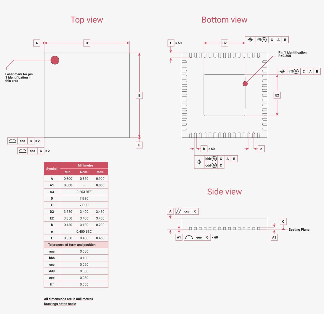
Figure 143 illustrates the mechanical details of the RP2350 QFN-60 package, showing the top view, bottom view, and side view.
Top view: Shows the package dimensions A, D, E, and B. A laser mark for pin 1 identification is indicated in the top-left corner. The package is marked with 'aaa C x 2' and 'aaa C x 2'.
Bottom view: Shows the package dimensions L, D2, E2, b, and e. The package is marked with 'fff (M) C A B' and 'Pin 1 identification R=0.200'. The package is marked with 'bbb (M) C A B' and 'ddd (M) C'.
Side view: Shows the package dimensions A, C, A1, A3, and the seating plane. The package is marked with 'ccc C' and 'eee C x 60'.
| Symbol | Millimetre | ||
|---|---|---|---|
| Min. | Nom. | Max. | |
| A | 0.800 | 0.850 | 0.900 |
| A1 | 0.000 | - | 0.050 |
| A3 | 0.203 REF | ||
| D | 7 BSC | ||
| E | 7 BSC | ||
| D2 | 3.350 | 3.400 | 3.450 |
| E2 | 3.350 | 3.400 | 3.450 |
| b | 0.130 | 0.180 | 0.230 |
| e | 0.400 BSC | ||
| L | 0.350 | 0.400 | 0.450 |
| Tolerances of form and position | |||
| aaa | 0.050 | ||
| bbb | 0.100 | ||
| ccc | 0.050 | ||
| ddd | 0.050 | ||
| eee | 0.080 | ||
| fff | 0.050 | ||
All dimensions are in millimetres
Drawings not to scale
NOTE
Leads have a matte Tin (Sn) finish. Annealing is done post-plating, baking at 150°C for 1 hour. Minimum thickness for lead plating is 8 microns, and the intermediate layer material is CuFe2P (roughened Copper (Cu)).
14.1.1. Thermal characteristics
The thermal characteristics of the QFN-60 package are shown in Table 1423 .
Table 1423. Thermal data for the QFN-60 package.
| Device | \( \theta_{JA} \) (°C/W) - Still Air | \( \theta_{JA} \) (°C/W) - 1m/s Forced Air | \( \theta_{JA} \) (°C/W) - 2m/s Forced Air | \( \theta_{JB} \) (°C/W) | \( \theta_{JC} \) (°C/W) |
|---|---|---|---|---|---|
| RP2350A | 40.542 | 31.99 | 30.264 | 12.588 | 14.315 |
| RP2354A | TBD | TBD | TBD | TBD | TBD |
14.1.2. Recommended PCB footprint
Figure 144. Recommended PCB Footprint for the RP2350 QFN-60 package
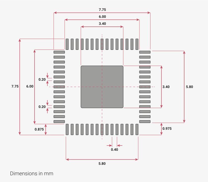
Figure 144 shows the recommended PCB footprint for the RP2350 QFN-60 package. The footprint is square, with overall dimensions of 7.75 mm by 7.75 mm. The central square area is 6.00 mm wide and 5.80 mm high. The footprint includes 60 leads, with dimensions for lead pitch (0.40 mm), lead width (0.20 mm), and lead spacing (0.875 mm). The footprint is shown with a central square area and four rectangular areas on the sides, each containing 15 leads. The dimensions are in mm.
14.2. QFN-80 package
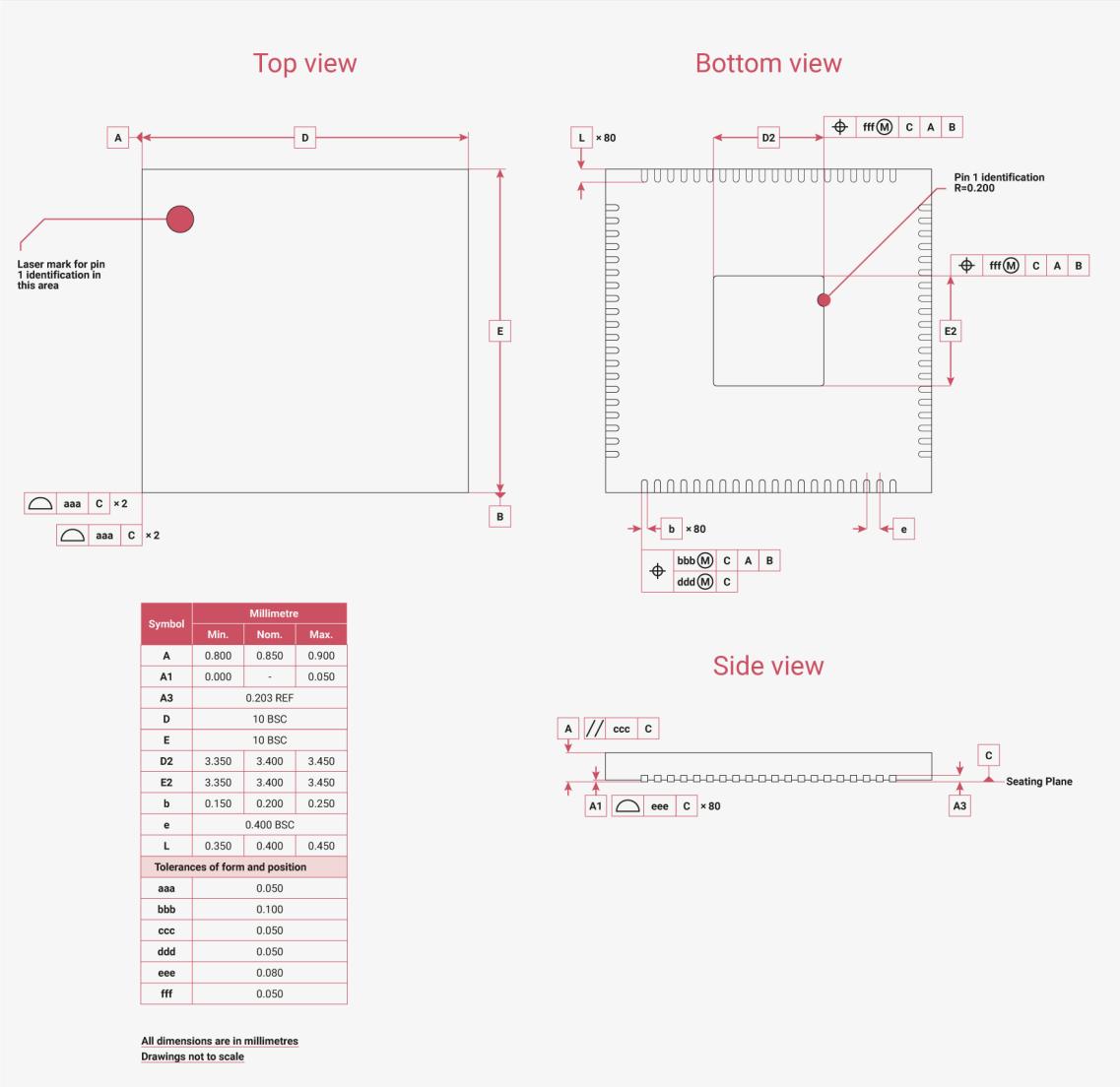
Figure 145. Top down view (left, top) and side view (right, bottom), along with bottom view (right, top) of the RP2350 QFN-80 package
| Symbol | Millimetre | ||
|---|---|---|---|
| Min. | Nom. | Max. | |
| A | 0.800 | 0.850 | 0.900 |
| A1 | 0.000 | - | 0.050 |
| A3 | 0.203 REF | ||
| D | 10 BSC | ||
| E | 10 BSC | ||
| D2 | 3.350 | 3.400 | 3.450 |
| E2 | 3.350 | 3.400 | 3.450 |
| b | 0.150 | 0.200 | 0.250 |
| e | 0.400 BSC | ||
| L | 0.350 | 0.400 | 0.450 |
| Tolerances of form and position | |||
| aaa | 0.050 | ||
| bbb | 0.100 | ||
| ccc | 0.050 | ||
| ddd | 0.050 | ||
| eee | 0.080 | ||
| fff | 0.050 | ||
All dimensions are in millimetres
Drawings not to scale
NOTE
Leads have a matte Tin (Sn) finish. Annealing is done post-plating, baking at 150°C for 1 hour. Minimum thickness for lead plating is 8 microns, and the intermediate layer material is CuFe2P (roughened Copper (Cu)).
14.2.1. Thermal characteristics
The thermal characteristics of the QFN-80 package are shown in Table 1424 .
Table 1424. Thermal data for the QFN-80 package.
| Device | \( \theta_{JA} \) (°C/W) - Still Air | \( \theta_{JA} \) (°C/W) - 1m/s Forced Air | \( \theta_{JA} \) (°C/W) - 2m/s Forced Air | \( \theta_{JB} \) (°C/W) | \( \theta_{JC} \) (°C/W) |
|---|---|---|---|---|---|
| RP2350B | TBD | TBD | TBD | TBD | TBD |
| RP2354B | TBD | TBD | TBD | TBD | TBD |
14.2.2. Recommended PCB footprint
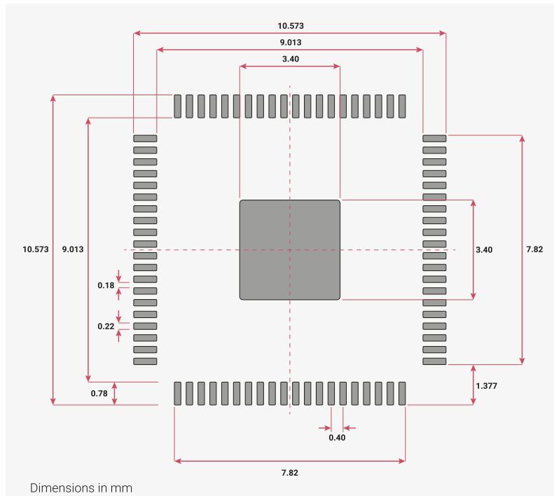
Figure 146.
Recommended PCB
Footprint for the
RP2350 QFN-80
package
- ◦ See Section 12.14 for more details of the RP2350 QSPI memory interface and its capabilities
The internal flash die can also be programmed externally by holding the RP2350 die in reset via the RUN pin (active-low reset), and driving QSPI signals into the chip from an external programmer.
The internal flash is powered by the QSPI_IOVDD supply input. This voltage must be in the range 2.7 to 3.6 V. You should account for the increased high-frequency currents on this supply pin in your decoupling circuit and PCB layout.
The maximum QSPI clock frequency of the W25Q16JVWI is 133 MHz. Consult the W25Q16JVWI datasheet for detailed timings and AC parameters.
If you do not require access to the RP2350 QSPI bus from the outside, you should minimise the track length connected to the QSPI package pins on your PCB. This avoids unnecessary emissions and capacitive loading of the QSPI bus.
The PADRESETB reset input on the W25Q16JVWI is not connected to any external package pins, or to any internal signals on the RP2350 die. This means there is no way to perform a hardware reset of the flash die. When the RP2350 die comes out of reset it initialises the flash die in the same way it would an external flash device by issuing a fixed XIP exit sequence that returns the flash die to a serial command state in preparation for execute-in-place setup.
14.4. Package markings
RP2350 comes in 7 × 7 mm QFN-60 and 10 × 10 mm QFN-80 packages, which are marked with the following data:
- • Pin 1 dot
- • Logo
- • Part number
- • Date code (Week)
- • Silicon lot number
- • Date code (Year)
The part number consists of the following:
- • Device name "RP2350"
- • Package type, "A" for QFN-60 or "B" for QFN-80
- • Package revision "0"
- • Die stepping "A2", "A3", or "A4"
See Appendix C for a summary of the differences between die steppings.
14.5. Storage conditions
To preserve the shelf and floor life of bare RP2350 devices, follow JEDEC J-STD (020E & 033D).
RP2350 QFN-60 is classified as Moisture Sensitivity Level 1 (MSL1). The MSL of QFN-80 is still being characterised and details will follow in a future datasheet update.
All RP2350 devices should be stored under 30°C and 85% relative humidity.
14.6. Solder profile
RP2350 is a Pb-free part, with a \( T_p \) value of 260°C.
All temperatures refer to the centre of the package, measured on the package body surface that faces up during
assembly reflow (live-bug orientation). If parts are reflowed in a different orientation (e.g. dead-bug), \( T_p \) shall be within \( \pm 2^\circ\text{C} \) of the live-bug \( T_p \) and still meet the \( T_c \) requirements; otherwise, you must adjust the profile to achieve the latter.
Figure 147.
Classification profile
(not to scale)
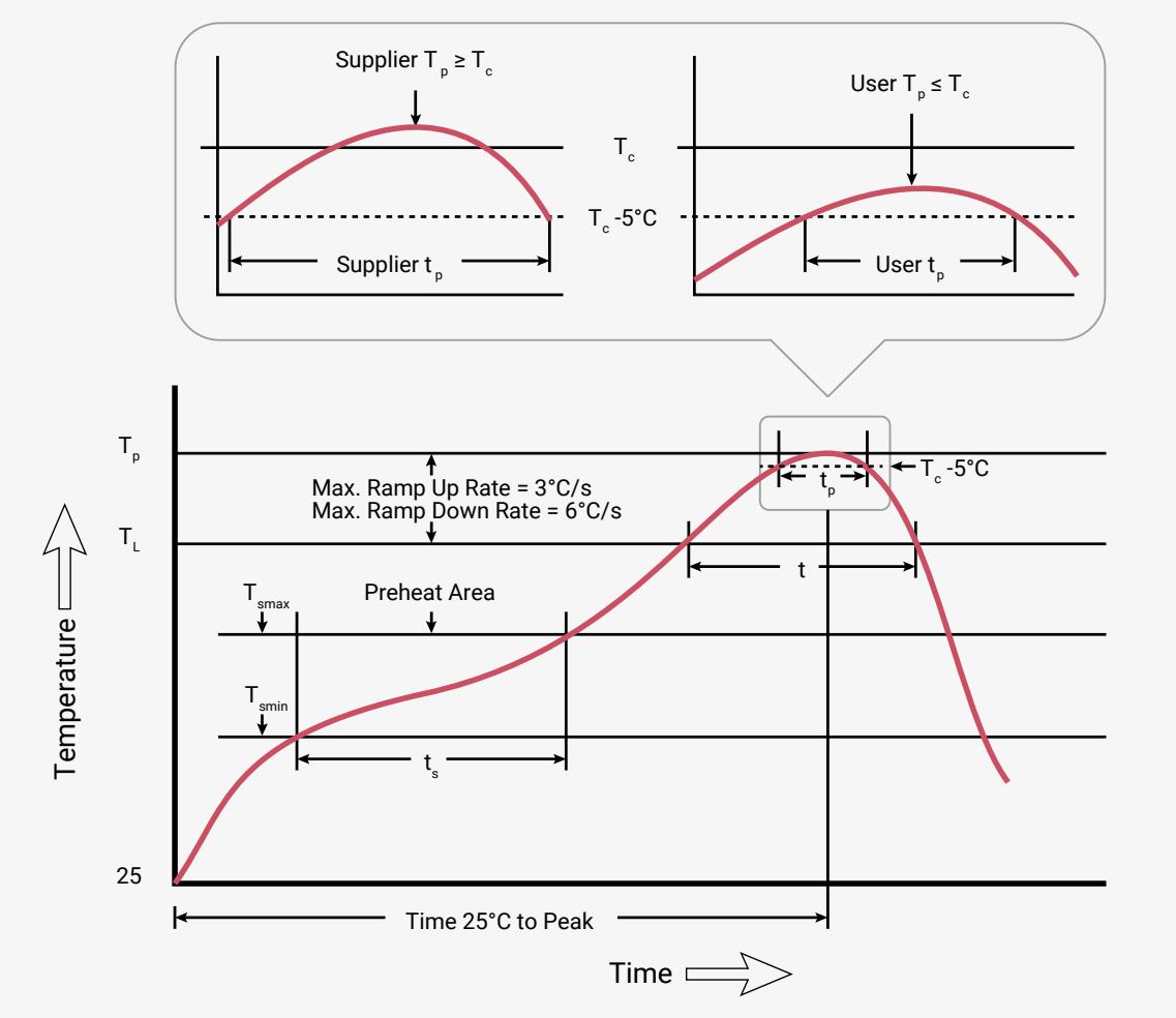
Reflow profiles in this document are for classification/preconditioning, and are not meant to specify board assembly profiles. Actual board assembly profiles should be developed based on specific process needs and board designs, and should not exceed the parameters in Table 1425 .
Table 1425. Solder
profile values
| Profile feature | Value |
|---|---|
| Temperature min ( \( T_{smin} \) ) | 150°C |
| Temperature max ( \( T_{smax} \) ) | 200°C |
| Time ( \( t_s \) ) from ( \( T_{smin} \) to \( T_{smax} \) ) | 60 - 120 seconds |
| Ramp-up rate ( \( T_L \) to \( T_p \) ) | 3°C/second max. |
| Liquidous temperature ( \( T_L \) ) | 217°C |
| Time ( \( t_L \) ) maintained above \( T_L \) | 60 to 150 seconds |
| Peak package body temperature ( \( T_p \) ) | 260°C |
| Classification temperature ( \( T_c \) ) | 260°C |
| Time ( \( t_p \) ) within 5°C of the specified classification temperature ( \( T_c \) ) | 30 seconds |
| Ramp-down rate ( \( T_p \) to \( T_L \) ) | 6°C/second max. |
| Time 25°C to peak temperature | 8 minutes max. |
14.7. Compliance
RP2350 QFN-60 is compliant to Moisture Sensitivity Level 1. The Moisture Sensitivity Level compliance of RP2350 QFN-80 is yet to be fully characterised, and details will follow in a future datasheet update.
RP2350 is compliant to the requirement of REACH Substances of Very High Concern (SVHC), EU ECHA directive.
RP2350 is compliant to the requirement and standard of Controlled Environment-related Substance of RoHS directive (EU) 2011/65/EU and directive (EU) 2015/863.
Raspberry Pi Ltd carried out the following Package Level reliability qualifications on RP2350:
- • Temperature Cycling per JESD22-A104
- • HAST per JESD22-A110
- • HTSL per JESD22-A103
- • MSL level per JESD22-A113
The following Silicon Level reliability qualification were also carried out:
- • HTOL per JESD22-A108F
 NOTE
NOTE
A tin whiskers test is not performed. RP2350 is a bottom-only termination device in the QFN-60 and QFN-80 packages, therefore JEDEC standard (JESD201A) is not applicable.
14.8. Pinout
14.8.1. Pin locations
14.8.1.1. QFN-60 (RP2350A)
Figure 148. RP2350
Pinout for QFN-60
7×7mm
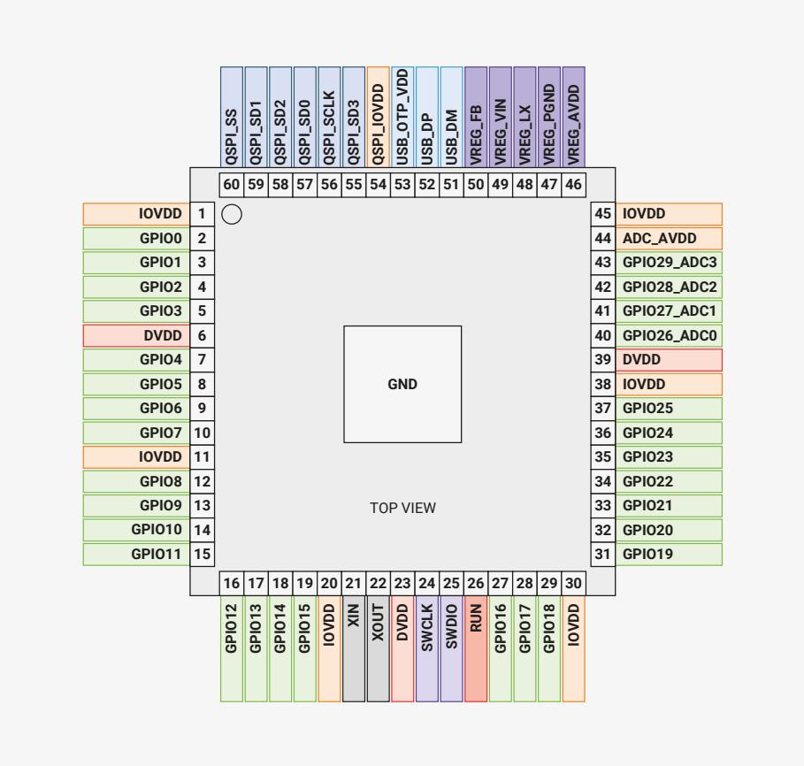
Pinout for QFN-60 (7×7mm):
| Pin | Signal |
|---|---|
| 1 | IOVDD |
| 2 | GPIO0 |
| 3 | GPIO1 |
| 4 | GPIO2 |
| 5 | GPIO3 |
| 6 | DVDD |
| 7 | GPIO4 |
| 8 | GPIO5 |
| 9 | GPIO6 |
| 10 | GPIO7 |
| 11 | IOVDD |
| 12 | GPIO8 |
| 13 | GPIO9 |
| 14 | GPIO10 |
| 15 | GPIO11 |
| 16 | GPIO12 |
| 17 | GPIO13 |
| 18 | GPIO14 |
| 19 | GPIO15 |
| 20 | IOVDD |
| 21 | XIN |
| 22 | XOUT |
| 23 | DVDD |
| 24 | SWCLK |
| 25 | SWDIO |
| 26 | RUN |
| 27 | GPIO16 |
| 28 | GPIO17 |
| 29 | GPIO18 |
| 30 | IOVDD |
| 31 | GPIO19 |
| 32 | GPIO20 |
| 33 | GPIO21 |
| 34 | GPIO22 |
| 35 | GPIO23 |
| 36 | GPIO24 |
| 37 | GPIO25 |
| 38 | IOVDD |
| 39 | DVDD |
| 40 | GPIO26_ADC0 |
| 41 | GPIO27_ADC1 |
| 42 | GPIO28_ADC2 |
| 43 | GPIO29_ADC3 |
| 44 | ADC_AVDD |
| 45 | IOVDD |
| 46 | VREG_AVDD |
| 47 | VREG_PGND |
| 48 | VREG_LX |
| 49 | VREG_VIN |
| 50 | VREG_FB |
| 51 | USB_DM |
| 52 | USB_DP |
| 53 | USB_OTP_VDD |
| 54 | QSPI_IOVDD |
| 55 | QSPI_SD3 |
| 56 | QSPI_SCLK |
| 57 | QSPI_SD0 |
| 58 | QSPI_SD2 |
| 59 | QSPI_SD1 |
| 60 | QSPI_SS |
14.8.1.2. QFN-80 (RP2350B)
Figure 149. RP2350
Pinout for QFN-80
10×10mm
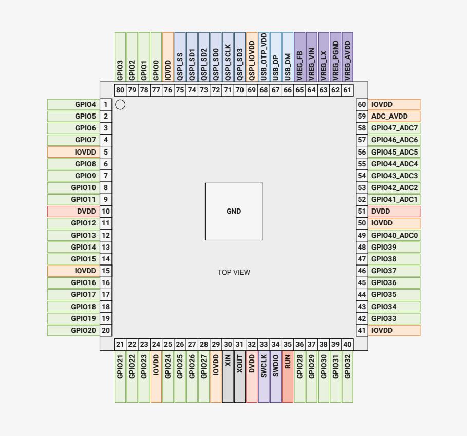
Pinout for QFN-80 (10×10mm):
| Pin | Signal |
|---|---|
| 1 | GPIO4 |
| 2 | GPIO5 |
| 3 | GPIO6 |
| 4 | GPIO7 |
| 5 | IOVDD |
| 6 | GPIO8 |
| 7 | GPIO9 |
| 8 | GPIO10 |
| 9 | GPIO11 |
| 10 | DVDD |
| 11 | GPIO12 |
| 12 | GPIO13 |
| 13 | GPIO14 |
| 14 | GPIO15 |
| 15 | IOVDD |
| 16 | GPIO16 |
| 17 | GPIO17 |
| 18 | GPIO18 |
| 19 | GPIO19 |
| 20 | GPIO20 |
| 21 | GPIO21 |
| 22 | GPIO22 |
| 23 | GPIO23 |
| 24 | IOVDD |
| 25 | GPIO24 |
| 26 | GPIO25 |
| 27 | GPIO26 |
| 28 | GPIO27 |
| 29 | IOVDD |
| 30 | XIN |
| 31 | XOUT |
| 32 | DVDD |
| 33 | SWCLK |
| 34 | SWDIO |
| 35 | RUN |
| 36 | GPIO28 |
| 37 | GPIO29 |
| 38 | GPIO30 |
| 39 | GPIO31 |
| 40 | GPIO32 |
| 41 | IOVDD |
| 42 | GPIO33 |
| 43 | GPIO34 |
| 44 | GPIO35 |
| 45 | GPIO36 |
| 46 | GPIO37 |
| 47 | GPIO38 |
| 48 | GPIO39 |
| 49 | GPIO40_ADC0 |
| 50 | IOVDD |
| 51 | DVDD |
| 52 | GPIO41_ADC1 |
| 53 | GPIO42_ADC2 |
| 54 | GPIO43_ADC3 |
| 55 | GPIO44_ADC4 |
| 56 | GPIO45_ADC5 |
| 57 | GPIO46_ADC6 |
| 58 | GPIO47_ADC7 |
| 59 | ADC_AVDD |
| 60 | IOVDD |
| 61 | VREG_AVDD |
| 62 | VREG_PGND |
| 63 | VREG_LX |
| 64 | VREG_VIN |
| 65 | VREG_FB |
| 66 | USB_DM |
| 67 | USB_DP |
| 68 | USB_OTP_VDD |
| 69 | QSPI_IOVDD |
| 70 | QSPI_SD3 |
| 71 | QSPI_SCLK |
| 72 | QSPI_SD0 |
| 73 | QSPI_SD2 |
| 74 | QSPI_SD1 |
| 75 | IOVDD |
| 76 | GPIO0 |
| 77 | GPIO1 |
| 78 | GPIO2 |
| 79 | GPIO3 |
| 80 | GPIO4 |
14.8.2. Pin definitions
14.8.2.1. Pin types
In the following pin tables ( Table 1427 ), the pin types are defined as shown below.
Table 1426. Pin Types
| Pin Type | Direction | Description |
|---|---|---|
| Digital In | Input only | Standard Digital. Programmable Pull-Up, Pull-Down, Slew Rate, Schmitt Trigger and Drive Strength. Default Drive Strength is 4 mA. |
| Digital IO | Bi-directional | |
| Digital In (FT) | Input only | Fault Tolerant Digital. These pins are described as Fault Tolerant, which in this case means that very little current flows into the pin whilst it is below 3.63 V and IOVDD is 0 V. Additionally, they will tolerate voltages up to 5.5 V, provided IOVDD is powered to 3.3 V. These pins have enhanced ESD protection. Programmable Pull-Up, Pull-Down, Slew Rate, Schmitt Trigger and Drive Strength. Default Drive Strength is 4 mA. |
| Digital IO (FT) | Bi-directional | |
| Digital IO / Analogue | Bi-directional (digital), Input (Analogue) | Standard Digital and ADC input. Programmable Pull-Up, Pull-Down, Slew Rate, Schmitt Trigger and Drive Strength. Default Drive Strength is 4 mA. |
| USB IO | Bi-directional | These pins are for USB use, and contain internal pull-up and pull-down resistors, as per the USB specification. USB operation requires external 27Ω series resistors. |
| Analogue (XOSC) | Oscillator input pins for attaching a 12 MHz crystal. Alternatively, XIN may be driven by a square wave. |
14.8.2.2. Pin list
Table 1427. GPIO pins
| Name | QFN-60 Number | QFN-80 Number | Type | Power Domain | Reset State | Description |
|---|---|---|---|---|---|---|
| GPI00 | 2 | 77 | Digital IO (FT) | IOVDD | Pull-Down | User IO |
| GPI01 | 3 | 78 | Digital IO (FT) | IOVDD | Pull-Down | User IO |
| GPI02 | 4 | 79 | Digital IO (FT) | IOVDD | Pull-Down | User IO |
| GPI03 | 5 | 80 | Digital IO (FT) | IOVDD | Pull-Down | User IO |
| GPI04 | 7 | 1 | Digital IO (FT) | IOVDD | Pull-Down | User IO |
| GPI05 | 8 | 2 | Digital IO (FT) | IOVDD | Pull-Down | User IO |
| GPI06 | 9 | 3 | Digital IO (FT) | IOVDD | Pull-Down | User IO |
| GPI07 | 10 | 4 | Digital IO (FT) | IOVDD | Pull-Down | User IO |
| GPI08 | 12 | 6 | Digital IO (FT) | IOVDD | Pull-Down | User IO |
| GPI09 | 13 | 7 | Digital IO (FT) | IOVDD | Pull-Down | User IO |
| GPI010 | 14 | 8 | Digital IO (FT) | IOVDD | Pull-Down | User IO |
| GPI011 | 15 | 9 | Digital IO (FT) | IOVDD | Pull-Down | User IO |
| GPI012 | 16 | 11 | Digital IO (FT) | IOVDD | Pull-Down | User IO |
| GPI013 | 17 | 12 | Digital IO (FT) | IOVDD | Pull-Down | User IO |
| GPI014 | 18 | 13 | Digital IO (FT) | IOVDD | Pull-Down | User IO |
| Name | QFN-60 Number | QFN-80 Number | Type | Power Domain | Reset State | Description |
|---|---|---|---|---|---|---|
| GPI015 | 19 | 14 | Digital IO (FT) | IOVDD | Pull-Down | User IO |
| GPI016 | 27 | 16 | Digital IO (FT) | IOVDD | Pull-Down | User IO |
| GPI017 | 28 | 17 | Digital IO (FT) | IOVDD | Pull-Down | User IO |
| GPI018 | 29 | 18 | Digital IO (FT) | IOVDD | Pull-Down | User IO |
| GPI019 | 31 | 19 | Digital IO (FT) | IOVDD | Pull-Down | User IO |
| GPI020 | 32 | 20 | Digital IO (FT) | IOVDD | Pull-Down | User IO |
| GPI021 | 33 | 21 | Digital IO (FT) | IOVDD | Pull-Down | User IO |
| GPI022 | 34 | 22 | Digital IO (FT) | IOVDD | Pull-Down | User IO |
| GPI023 | 35 | 23 | Digital IO (FT) | IOVDD | Pull-Down | User IO |
| GPI024 | 36 | 25 | Digital IO (FT) | IOVDD | Pull-Down | User IO |
| GPI025 | 37 | 26 | Digital IO (FT) | IOVDD | Pull-Down | User IO |
| GPI026_ADC0 | 40 | - | Digital IO / Analogue | IOVDD / ADC_AVDD | Pull-Down | User IO or ADC input |
| GPI027_ADC1 | 41 | - | Digital IO / Analogue | IOVDD / ADC_AVDD | Pull-Down | User IO or ADC input |
| GPI028_ADC2 | 42 | - | Digital IO / Analogue | IOVDD / ADC_AVDD | Pull-Down | User IO or ADC input |
| GPI029_ADC3 | 43 | - | Digital IO / Analogue | IOVDD / ADC_AVDD | Pull-Down | User IO or ADC input |
| GPI026 | - | 27 | Digital IO (FT) | IOVDD | Pull-Down | User IO |
| GPI027 | - | 28 | Digital IO (FT) | IOVDD | Pull-Down | User IO |
| GPI028 | - | 36 | Digital IO (FT) | IOVDD | Pull-Down | User IO |
| GPI029 | - | 37 | Digital IO (FT) | IOVDD | Pull-Down | User IO |
| GPI030 | - | 38 | Digital IO (FT) | IOVDD | Pull-Down | User IO |
| GPI031 | - | 39 | Digital IO (FT) | IOVDD | Pull-Down | User IO |
| GPI032 | - | 40 | Digital IO (FT) | IOVDD | Pull-Down | User IO |
| GPI033 | - | 42 | Digital IO (FT) | IOVDD | Pull-Down | User IO |
| GPI034 | - | 43 | Digital IO (FT) | IOVDD | Pull-Down | User IO |
| GPI035 | - | 44 | Digital IO (FT) | IOVDD | Pull-Down | User IO |
| GPI036 | - | 45 | Digital IO (FT) | IOVDD | Pull-Down | User IO |
| GPI037 | - | 46 | Digital IO (FT) | IOVDD | Pull-Down | User IO |
| GPI038 | - | 47 | Digital IO (FT) | IOVDD | Pull-Down | User IO |
| GPI039 | - | 48 | Digital IO (FT) | IOVDD | Pull-Down | User IO |
| GPI040_ADC0 | - | 49 | Digital IO / Analogue | IOVDD / ADC_AVDD | Pull-Down | User IO or ADC input |
| GPI041_ADC1 | - | 52 | Digital IO / Analogue | IOVDD / ADC_AVDD | Pull-Down | User IO or ADC input |
| Name | QFN-60 Number | QFN-80 Number | Type | Power Domain | Reset State | Description |
|---|---|---|---|---|---|---|
| GPI042_ADC2 | - | 53 | Digital IO / Analogue | IOVDD / ADC_AVDD | Pull-Down | User IO or ADC input |
| GPI043_ADC3 | - | 54 | Digital IO / Analogue | IOVDD / ADC_AVDD | Pull-Down | User IO or ADC input |
| GPI044_ADC4 | - | 55 | Digital IO / Analogue | IOVDD / ADC_AVDD | Pull-Down | User IO or ADC input |
| GPI045_ADC5 | - | 56 | Digital IO / Analogue | IOVDD / ADC_AVDD | Pull-Down | User IO or ADC input |
| GPI046_ADC6 | - | 57 | Digital IO / Analogue | IOVDD / ADC_AVDD | Pull-Down | User IO or ADC input |
| GPI047_ADC7 | - | 58 | Digital IO / Analogue | IOVDD / ADC_AVDD | Pull-Down | User IO or ADC input |
Table 1428. QSPI pins
| Name | QFN-60 Number | QFN-80 Number | Type | Power Domain | Reset State | Description |
|---|---|---|---|---|---|---|
| QSPI_SD3 | 55 | 70 | Digital IO | QSPI_IOVDD | Pull-Up | QSPI data |
| QSPI_SCLK | 56 | 71 | Digital IO | QSPI_IOVDD | Pull-Down | QSPI clock |
| QSPI_SD0 | 57 | 72 | Digital IO | QSPI_IOVDD | Pull-Down | QSPI data |
| QSPI_SD2 | 58 | 73 | Digital IO | QSPI_IOVDD | Pull-Up | QSPI data |
| QSPI_SD1 | 59 | 74 | Digital IO | QSPI_IOVDD | Pull-Down | QSPI data |
| QSPI_SS | 60 | 75 | Digital IO | QSPI_IOVDD | Pull-Up | QSPI chip select / USB BOOTSEL |
Table 1429. Crystal oscillator pins
| Name | QFN-60 Number | QFN-80 Number | Type | Power Domain | Description |
|---|---|---|---|---|---|
| XIN | 21 | 30 | Analogue (XOSC) | IOVDD | Crystal oscillator. XIN may also be driven by a square wave. |
| XOUT | 22 | 31 | Analogue (XOSC) | IOVDD | Crystal oscillator. |
Table 1430. Miscellaneous pins
| Name | QFN-60 Number | QFN-80 Number | Type | Power Domain | Reset State | Description |
|---|---|---|---|---|---|---|
| RUN | 26 | 35 | Digital In (FT) | IOVDD | Pull-Up | Chip enable / reset_n |
| SWCLK | 24 | 33 | Digital In (FT) | IOVDD | Pull-Up | Serial Wire Debug clock |
| SWDIO | 25 | 34 | Digital IO (FT) | IOVDD | Pull-Up | Serial Wire Debug data |
Table 1431. USB pins
| Name | QFN-60 Number | QFN-80 Number | Type | Power Domain | Description |
|---|---|---|---|---|---|
| USB_DP | 52 | 67 | USB IO | USB_OTP_VDD | USB Data +ve. 27Ω series resistor required for USB operation |
| Name | QFN-60 Number | QFN-80 Number | Type | Power Domain | Description |
|---|---|---|---|---|---|
| USB_DM | 51 | 66 | USB IO | USB_OTP_VDD | USB Data -ve. 27Ω series resistor required for USB operation |
Table 1432. Power supply pins
| Name | QFN-60 Number(s) | QFN-80 Number(s) | Description |
|---|---|---|---|
| DVDD | 6, 23, 39 | 10, 32, 51 | Core supply |
| IOVDD | 11, 20, 30, 38, 45, 54 | 5, 15, 24, 29, 41, 50, 60, 76 | IO supply |
| QSPI_IOVDD | 54 | 69 | QSPI IO supply |
| USB_OTP_VDD | 53 | 68 | USB & OTP supply |
| ADC_AVDD | 44 | 59 | ADC supply |
| VREG_AVDD | 46 | 61 | Voltage regulator analogue supply |
| VREG_PGND | 47 | 62 | Voltage regulator ground |
| VREG_LX | 48 | 63 | Voltage regulator switching output (connect to inductor) |
| VREG_VIN | 49 | 64 | Voltage regulator input supply |
| VREG_FB | 50 | 65 | Voltage regulator feedback input |
| GND | - | - | Ground connection via central exposed pad |
14.9. Electrical specifications
The following electrical specifications are obtained from characterisation over the specified temperature and voltage ranges, as well as process variation, unless the specification is marked as 'Simulated'. In this case, the data is for information purposes only, and is not guaranteed.
14.9.1. Absolute maximum ratings
Stresses beyond the absolute maximum ratings listed in the following table can cause permanent damage to the device. These are stress ratings only and do not refer to the functional operation of the device.
Table 1433. Absolute maximum ratings
| Parameter | Symbol | Conditions | Minimum | Maximum | Units | Comment |
|---|---|---|---|---|---|---|
| Core Supply (DVDD) Voltage | DVDD | -0.5 | 1.21 | V | ||
| I/O Supply (IOVDD) & QSPI Supply (QSPI_IOVDD) Voltage | IOVDD | -0.5 | 3.63 | V |
| Parameter | Symbol | Conditions | Minimum | Maximum | Units | Comment |
|---|---|---|---|---|---|---|
| Voltage at IO (Standard) | V PIN | -0.5 | IOVDD + 0.5 | V | ||
| Voltage at IO (FT) | V PIN_FT | IOVDD=3.3V | -0.5 | 5.5 | V | IOVDD must be present |
| IOVDD=2.5V | -0.5 | 4.2 | V | |||
| IOVDD=1.8V | -0.5 | 3.63 | V | |||
| IOVDD=0V | -0.5 | 3.63 | V | |||
| Junction temperature | -40 | 125 | °C | |||
| Storage temperature | 150 | °C |
14.9.2. ESD performance
Table 1434. ESD performance for all pins, unless otherwise stated
| Parameter | Symbol | Maximum | Units | Comment |
|---|---|---|---|---|
| Human Body Model | HBM | 2 | kV | Compliant with JEDEC specification JS-001-2012 (April 2012) |
| Human Body Model Digital (FT) pins only | HBM | 4 | kV | Compliant with JEDEC specification JS-001-2012 (April 2012) |
| Charged Device Model | CDM | 500 | V | Compliant with JESD22-C101E (December 2009) |
14.9.3. Thermal performance
Table 1435. Thermal Performance
| Parameter | Symbol | Minimum | Typical | Maximum | Units | Comment |
|---|---|---|---|---|---|---|
| Ambient Temperature | T C | -40 | 85 | °C |
14.9.4. IO electrical characteristics
Table 1436. Digital IO characteristics - Standard and FT unless otherwise stated. In this table IOVDD also refers to QSPI_IOVDD where appropriate
| Parameter | Symbol | Conditions | Minimum | Maximum | Units | Comment |
|---|---|---|---|---|---|---|
| Pin Input Leakage Current | I IN | 1 | µA | |||
| Input Voltage High (Standard IO) | V IH | IOVDD=1.8V | 0.65 * IOVDD | IOVDD + 0.3 | V | |
| IOVDD=2.5V | 1.7 | IOVDD + 0.3 | V | |||
| IOVDD=3.3V | 2 | IOVDD + 0.3 | V |
| Parameter | Symbol | Conditions | Minimum | Maximum | Units | Comment |
|---|---|---|---|---|---|---|
| Input Voltage High (FT) | \( V_{IH} \) | IOVDD=1.8V | \( 0.65 * IOVDD \) | 3.63 | V | IOVDD must be powered to tolerate input voltages above 3.63V |
| IOVDD=2.5V | 1.7 | 4.2 | V | |||
| IOVDD=3.3V | 2 | 5.5 | V | |||
| Input Voltage Low | \( V_{IL} \) | IOVDD=1.8V | -0.3 | \( 0.35 * IOVDD \) | V | |
| IOVDD=2.5V | -0.3 | 0.7 | V | |||
| IOVDD=3.3V | -0.3 | 0.8 | V | |||
| Input Hysteresis Voltage | \( V_{HYS} \) | IOVDD=1.8V | \( 0.1 * IOVDD \) | V | Schmitt Trigger enabled | |
| IOVDD=2.5V | 0.2 | V | ||||
| IOVDD=3.3V | 0.2 | V | ||||
| Output Voltage High | \( V_{OH} \) | IOVDD=1.8V | 1.24 | IOVDD | V | \( I_{OH} = 2, 4, 8 \) or \( 12mA \) depending on setting |
| IOVDD=2.5V | 1.78 | IOVDD | V | |||
| IOVDD=3.3V | 2.62 | IOVDD | V | |||
| Output Voltage Low | \( V_{OL} \) | IOVDD=1.8V | 0 | 0.3 | V | \( I_{OL} = 2, 4, 8 \) or \( 12mA \) depending on setting |
| IOVDD=2.5V | 0 | 0.4 | V | |||
| IOVDD=3.3V | 0 | 0.5 | V | |||
| Pull-Up Resistance | \( R_{PU} \) | IOVDD=1.8V | 32 | 106 | k \( \Omega \) | |
| IOVDD=2.5V | 42 | 123 | k \( \Omega \) | |||
| IOVDD=3.3V | 32 | 86 | k \( \Omega \) | |||
| Pull-Down Resistance | \( R_{PD} \) | IOVDD=1.8V | 35 | 189 | k \( \Omega \) | |
| IOVDD=2.5V | 49 | 180 | k \( \Omega \) | |||
| IOVDD=3.3V | 36 | 113 | k \( \Omega \) | |||
| Maximum Total IOVDD current | \( I_{IOVDD\_MAX} \) | 100 | mA | Sum of all current being sourced by GPIO pins | ||
| Maximum Total QSPI_IOVDD current | \( I_{QSPI\_IOVDD\_MAX} \) | 20 | mA | Sum of all current being sourced by QSPI pins | ||
| Maximum Total VSS current due to GPIO (IOVSS) | \( I_{IOVSS\_MAX} \) | 100 | mA | Sum of all current being sunk into GPIO pins | ||
| Maximum Total VSS current due to QSPI (QSPL_IOVSS) | \( I_{QSPL\_IOVSS\_MAX} \) | 20 | mA | Sum of all current being sunk into QSPI pins |
Table 1437. USB IO characteristics
| Parameter | Symbol | Minimum | Maximum | Units | Comment |
|---|---|---|---|---|---|
| Pin Input Leakage Current | \( I_{IN} \) | 1 | \( \mu A \) | ||
| Single Ended Input Voltage High | \( V_{IHSE} \) | 2 | V | ||
| Single Ended Input Voltage Low | \( V_{ILSE} \) | 0.8 | V | ||
| Differential Input Voltage High | \( V_{IHDIFF} \) | 0.2 | V | ||
| Differential Input Voltage Low | \( V_{ILDIFF} \) | -0.2 | V | ||
| Output Voltage High | \( V_{OH} \) | 2.8 | USB_OTG_VDD | V | |
| Output Voltage Low | \( V_{OL} \) | 0 | 0.3 | V | |
| Pull-Up Resistance - RPU2 | \( R_{PU2} \) | 0.873 | 1.548 | k \( \Omega \) | |
| Pull-Up Resistance - RPU1&2 | \( R_{PU1\&2} \) | 1.398 | 3.063 | k \( \Omega \) | |
| Pull-Down Resistance | \( R_{PD} \) | 14.25 | 15.75 | k \( \Omega \) |
Table 1438. ADC characteristics
| Parameter | Symbol | Minimum | Typical | Maximum | Units | Comment |
|---|---|---|---|---|---|---|
| ADC Input Voltage Range | \( V_{PIN\_ADC} \) | 0 | ADC_AVDD | V | ||
| Effective Number of Bits | ENOB | 9 | 9.5 | bits | ||
| Resolved Bits | 12 | bits | ||||
| ADC Input Impedance | \( R_{IN\_ADC} \) | 100 | k \( \Omega \) |
Table 1439. Oscillator pin characteristics
| Parameter | Symbol | Minimum | Typical | Maximum | Units | Comment |
|---|---|---|---|---|---|---|
| Input Frequency | \( f_{osc} \) | 1 | 12 | 50 | MHz | See
Section 8.6.3
for restrictions imposed by PLLs. See Section 5.2.8.1 for restrictions imposed by the USB and UART bootloaders. |
| Parameter | Symbol | Minimum | Typical | Maximum | Units | Comment |
|---|---|---|---|---|---|---|
| Input Voltage High | \( V_{IH} \) | \( 0.65 \cdot IOVDD \) | \( IOVDD + 0.3 \) | V | Square Wave input. XIN only. XOUT floating | |
| Input Voltage Low | \( V_{IL} \) | 0 | \( 0.35 \cdot IOVDD \) | V | Square Wave input. XIN only. XOUT floating |
NOTE
By default, USB Bootmode relies on a 12MHz input being present. However OTP can be configured to override the XOSC and PLL settings during USB Bootmode. See Section 13.10 for details.
Table 1440. SWCLK pin characteristics
| Parameter | Symbol | Minimum | Typical | Maximum | Units | Comment |
|---|---|---|---|---|---|---|
| SWCLK Input Frequency | \( f_{SWCLK} \) | 0 | 10 | 50 | MHz | See Table 1430 for SWCLK pin definitions. |
Host-to-target data on the SWDIO pin should be transmitted centre-aligned with SWCLK . Target-to-host data on the SWDIO pin transitions on rising edges of SWCLK .
NOTE
RP2350 internal SWD logic in the SW-DP operates reliably up to 50 MHz. However, signal integrity of the external SWD signals may be a challenge.
If you observe unreliable SWD operation such as write data parity errors from the SW-DP, reduce the SWCLK frequency. Always connect ground directly between the SWD probe and RP2350 in addition to SWDIO and SWCLK . Minimise the wire length between the probe and RP2350, and avoid multi-drop wiring at higher frequencies.
14.9.4.1. Interpreting GPIO output voltage specifications
The GPIOs on RP2350 have four different output drive strengths, nominally called 2, 4, 8 and 12mA modes. These are not hard limits, nor do they mean that they will always source (or sink) the selected amount of milliamps.
The amount of current a GPIO sources or sinks is dependent on the load attached. It will attempt to drive the output to the IOVDD level (or 0V in the case of a logic 0), but the amount of current it is able to source is limited and dependent on the selected drive strength.
Therefore the higher the current load is, the lower the voltage will be at the pin. At some point, the GPIO will source so much current and the voltage will drop so low that it won't be recognised as a logic 1 by the input of a connected device. The output specifications in Table 1436 quantify how much lower the voltage can be expected to be when drawing specified amounts of current from the pin.
The Output High Voltage ( \( V_{OH} \) ) is defined as the lowest voltage the output pin can be when driven to a logic 1 with a particular selected drive strength; e.g., 4mA sourced by the pin whilst in 4mA drive strength mode. The Output Low Voltage is similar, but with a logic 0 being driven.
In addition to this, the sum of all the IO currents being sourced (i.e. when outputs are being driven high) from the IOVDD bank (essentially the GPIO and QSPI pins), must not exceed \( I_{IOVDD\_MAX} \) . Similarly, the sum of all the IO currents being sunk (i.e. when the outputs are being driven low) must not exceed \( I_{IOVSS\_MAX} \) .
Figure 150. Typical Current vs Voltage curves of a GPIO output.
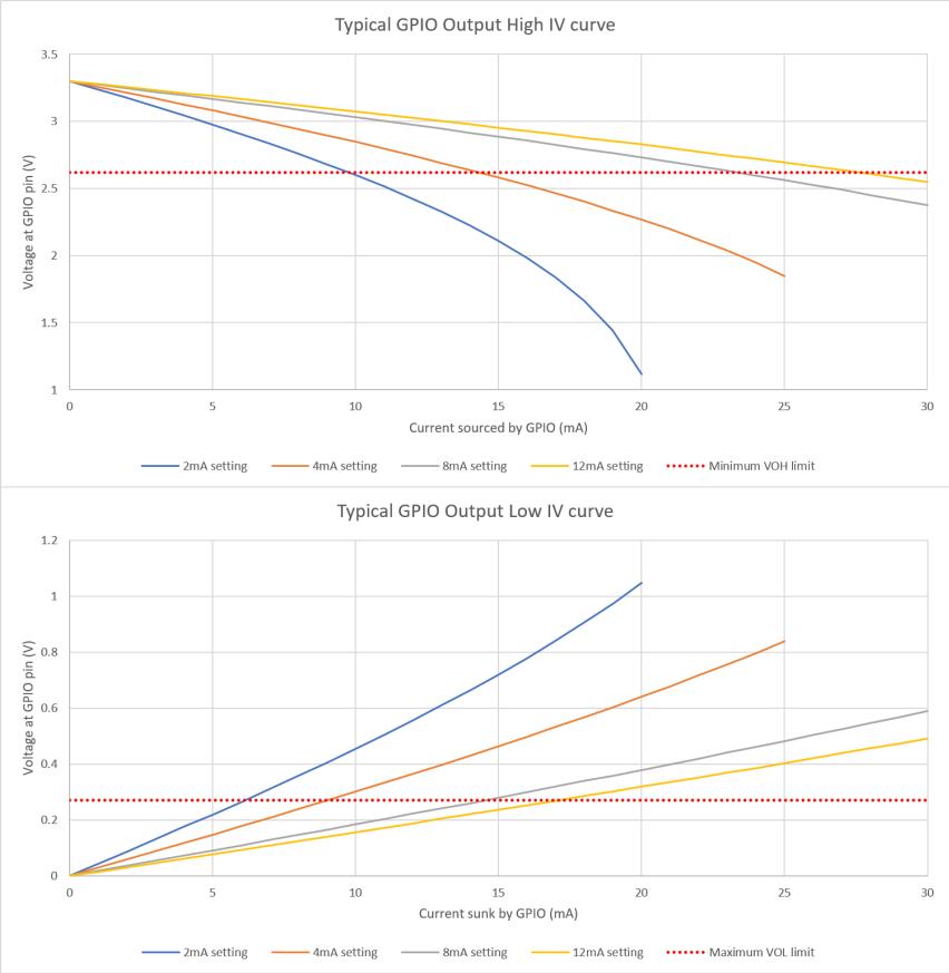
Typical GPIO Output High IV curve
| Current sourced by GPIO (mA) | 2mA setting (V) | 4mA setting (V) | 8mA setting (V) | 12mA setting (V) |
|---|---|---|---|---|
| 0 | 3.3 | 3.3 | 3.3 | 3.3 |
| 5 | 3.0 | 3.1 | 3.2 | 3.2 |
| 10 | 2.5 | 2.8 | 3.0 | 3.1 |
| 15 | 2.0 | 2.5 | 2.8 | 3.0 |
| 20 | 1.5 | 2.2 | 2.6 | 2.8 |
| 25 | - | 1.8 | 2.4 | 2.6 |
| 30 | - | - | 2.2 | 2.5 |
Typical GPIO Output Low IV curve
| Current sunk by GPIO (mA) | 2mA setting (V) | 4mA setting (V) | 8mA setting (V) | 12mA setting (V) |
|---|---|---|---|---|
| 0 | 0.0 | 0.0 | 0.0 | 0.0 |
| 5 | 0.2 | 0.15 | 0.1 | 0.08 |
| 10 | 0.4 | 0.3 | 0.2 | 0.15 |
| 15 | 0.7 | 0.45 | 0.3 | 0.25 |
| 20 | 1.0 | 0.6 | 0.4 | 0.35 |
| 25 | - | 0.8 | 0.5 | 0.45 |
| 30 | - | - | 0.6 | 0.5 |
Figure 150 shows the effect on the output voltage as the current load on the pin increases. You can clearly see the effect of the different drive strengths; the higher the drive strength, the closer the output voltage is to IOVDD (or 0V) for a given current. The minimum \( V_{OH} \) and maximum \( V_{OL} \) limits are shown in red.
You can see that at the specified current for each drive strength, the voltage is well within the allowed limits, meaning that this particular device could drive a lot more current and still be within \( V_{OH}/V_{OL} \) specification. This is a typical part at room temperature, but because devices vary, there will be a spread of other devices which will have voltages much closer to this limit.
If your application doesn't need such tightly controlled voltages, you can source or sink more current from the GPIO than the selected drive strength setting. However, experimentation is required to determine if it indeed safe to do so in your application.
14.9.5. Power supplies
Table 1441. Power Supply Specifications
| Power Supply | Supplies | Min | Typ | Max | Units |
|---|---|---|---|---|---|
| IOVDD a | Digital IO | 1.62 | 1.8 / 3.3 | 3.63 | V |
| QSPI_IOVDD (RP2350 only) a | Digital IO | 1.62 | 1.8 / 3.3 | 3.63 | V |
| QSPI_IOVDD (RP2354 only) | Digital IO | 2.97 | 3.3 | 3.63 | V |
| DVDD b | Digital core | 1.05 | 1.1 | 1.16 | V |
| VREG_VIN | Voltage regulator | 2.7 | 3.3 | 5.5 | V |
| VREG_AVDD | Voltage regulator | 3.135 | 3.3 | 3.63 | V |
| Power Supply | Supplies | Min | Typ | Max | Units |
|---|---|---|---|---|---|
| USB_OTP_VDD | USB PHY & OTP | 3.135 | 3.3 | 3.63 | V |
| ADC_AVDD c | ADC | 1.62 | 3.3 | 3.63 | V |
a
If IOVDD <2.5V, GPIO
VOLTAGE_SELECT
registers should be adjusted accordingly. See
Section 6.1
for details.
b Short term transients should be within +/-100mV.
c ADC performance will be compromised at voltages below 2.97V
i NOTE
RP2354 contains an internal 3.3V flash device, therefore
QSPI_IOVDD
must be 3.3V. Furthermore, if the QSPI pins are to be used to connect to an additional flash or PSRAM device, then IOVDD must be 3.3V, as a GPIO is used as QSPI chip select in this case.
14.9.6. Core voltage regulator
Table 1442. Voltage Regulator Specifications
| Parameter | Description | Min | Typ | Max | Units |
|---|---|---|---|---|---|
| V OUT (normal mode) | regulated output voltage range (normal mode) | 0.55 | 1.1 | 3.3 | V |
| V OUT (low power mode) | regulated output voltage range (low power mode) | 0.55 | 1.1 | 1.3 | V |
| ΔV OUT (normal mode) | voltage deviation from programmed value (normal mode) | -3 | +3 | % of selected output voltage | |
| ΔV OUT (low power mode) | voltage deviation from programmed value (low power mode) | -9 | +9 | % of selected output voltage | |
| I MAX (normal mode) | output current (normal mode) | 200 | mA | ||
| I MAX (low power mode) | output current (low power mode) | 1 | mA | ||
| I LIMIT (normal mode startup) | current limit (normal mode startup) | 240 | 300 | mA | |
| I LIMIT (normal mode) | current limit (normal mode) | 260 | 500 | 800 | mA |
| I LIMIT (low power mode) | current limit (low power mode) | 5 | 25 | mA | |
| VOUT_OK TH.ASSERT | VOUT_OK
assertion threshold | 87 | 90 | 93 | % of selected output voltage |
| Parameter | Description | Min | Typ | Max | Units |
|---|---|---|---|---|---|
| VOUT_OK TH.DEASSERT | VOUT_OK de-assertion threshold | 84 | 87 | 90 | % of selected output voltage |
| f sw | switching frequency | 3 | MHz | ||
| Efficiency (V OUT =1.1V) | I load =10mA, VREG_VIN=2.7V | 74 | % | ||
| I load =10mA, VREG_VIN=3.3V | 70 | % | |||
| I load =10mA, VREG_VIN=5.5V | 59 | % | |||
| I load =100mA, VREG_VIN=2.7V | 70 | % | |||
| I load =100mA, VREG_VIN=3.3V | 72 | % | |||
| I load =100mA, VREG_VIN=5.5V | 72 | % | |||
| I load =200mA, VREG_VIN=2.7V | 70 | % | |||
| I load =200mA, VREG_VIN=3.3V | 59 | % | |||
| I load =200mA, VREG_VIN=5.5V | 63 | % |
WARNING
V OUT can exceed the maximum core supply (DVDD). While there is a voltage limit to prevent this happening accidentally, the limit can be disabled under software control. For reliable operation DVDD should not exceed its maximum voltage rating.
Figure 151. Typical Regulator Efficiency, V OUT =1.1V, VREG_VIN=3.3V.
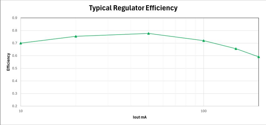
The graph shows the typical regulator efficiency as a function of output current (I out ) in mA. The y-axis represents Efficiency, ranging from 0.2 to 0.9. The x-axis represents I out in mA, with major ticks at 10 and 100. The efficiency curve starts at approximately 0.70 at 10mA, rises to a peak of about 0.78 at 50mA, and then gradually declines to approximately 0.60 at 200mA.
| I out (mA) | Efficiency |
|---|---|
| 10 | 0.70 |
| 50 | 0.78 |
| 100 | 0.72 |
| 150 | 0.68 |
| 200 | 0.60 |
14.9.7. Power consumption
14.9.7.1. Peripheral power consumption
Baseline readings are taken with only clock sources and essential peripherals (BUSCTRL, BUSFAB, VREG, Resets, ROM, SRAMs) active in the
WAKE_EN0/WAKE_EN1
registers. Clocks are set to default clock settings.
Each peripheral is activated in turn by enabling all clock sources for the peripheral in the
WAKE_EN0/WAKE_EN1
registers. Current consumption is the increase in current when the peripheral clocks are enabled.
Table 1443. Baseline power consumption
| Peripheral | Typical DVDD Current Consumption (µA/MHz) |
|---|---|
| DMA | 2.6 |
| I2C0 | 3 |
| I2C1 | 3.6 |
| IO + Pads | 24.5 |
| PWM | 9.9 |
| SIO | 2 |
| SHA256 | 0.1 |
| SPI0 | 1.7 |
| SPI1 | 1.4 |
| Timer 0 | 0.8 |
| Timer 1 | 0.6 |
| TRNG | 0.8 |
| UART0 | 2.6 |
| UART1 | 3.6 |
| Watchdog | 1.1 |
| XIP | 37.6 |
Because of fixed reference clocks of 48MHz, as well as the variable system clock input, ADC and USBCTRL power consumption does not vary linearly with system clock (as it does for other peripherals which only have system and/or peripheral clock inputs). The following table shows absolute DVDD current consumption of the ADC and USBCTRL blocks at standard clocks settings:
Table 1444. Baseline power consumption for ADC and USBCTRL
| Peripheral | Typical DVDD Current Consumption (mA) |
|---|---|
| ADC | 0.14 |
| USBCTRL | 1.25 |
14.9.7.2. Power consumption in Low Power states
Table 1445 shows the typical power consumption in low power states
P1.0
→
P1.7
. All voltage supplies are 3.3V (except DVDD which is supplied by the voltage regulator (in low power mode)), with the environment at room temperature.
All GPIOs,
SWDIO
and
SWCLK
are pulled down internally, and not connected externally. QSPI is connected to W25Q16JVSSIQ flash device. USB PHY has been powered down, and the
DP
and
DM
pull-downs were enabled prior to entering the low power state. The USB cable remains connected to a host computer. The table also shows the power consumed when
RUN
is held low. This is not technically a low power state (the voltage regulator is in normal switching mode), but it is included for completeness.
Table 1445. Low Power States Power Consumption
| Low Power State | VREG_VIN (μA) | VREG_AVDD (μA) | IOVDD (μA) | QSPI_IOVDD (μA) | ADC_IOVDD (μA) | USB_OTP_VDD (μA) | Total Power (μW) |
|---|---|---|---|---|---|---|---|
| P1.0 | 128 | 0.5 | 11 | 22 | 1 | 3.5 | 548 |
| P1.1 | 77 | 0.5 | 11 | 22 | 1 | 3.5 | 380 |
| P1.2 | 79 | 0.5 | 11 | 22 | 1 | 3.5 | 380 |
| P1.3 | 26 | 0.5 | 11 | 22 | 1 | 3.5 | 204 |
| P1.4 | 120 | 0.5 | 11 | 22 | 1 | 3.5 | 520 |
| P1.5 | 67 | 0.5 | 11 | 22 | 1 | 3.5 | 345 |
| P1.6 | 68 | 0.5 | 11 | 22 | 1 | 3.5 | 350 |
| P1.7 | 19 | 0.5 | 11 | 22 | 1 | 3.5 | 188 |
| RUN=low | 40 | 187 | 69 | 22 | 1 | 35 | 1170 |
14.9.7.3. Power consumption for typical user cases
The following table details the typical power consumption of RP2350 in various example use cases. All measurements were taken using 3.3V voltage supplies (except DVDD, which is supplied by the voltage regulator (set to 1.1V)), with the environment at room temperature.
SWD and SWCLK are not connected externally. GPIO0 and GPIO1 are connected to a Raspberry Pi Debug Probe (UART), but all other GPIOs are not connected (except USB Boot mode, where GPIO0 and GPIO1 are also unconnected). QSPI is connected to W25Q16JVSSIQ flash device, and USB is connected to a host.
hello_serial , hello_usb and hello_adc are basic applications found in pico-examples where characters are constantly transmitted to a serial console.
Table 1446. Power Consumption
| Use Case | Condition | VREG_VIN (μA) | VREG_AVDD (μA) | IOVDD (μA) | QSPI_IOVDD (μA) | ADC_IOVDD (μA) | USB_OTP_VDD (μA) | Total Power (mW) |
|---|---|---|---|---|---|---|---|---|
| USB Boot mode | Bus Idle (average) | 6530 | 220 | 437 | 22 | 1 | 375 | 25 |
| During Boot (peak) | 6050 | |||||||
| During UF2 write (average) | 1280 | |||||||
| hello_serial | 14690 | 216 | 506 | 22 | 1 | 62 | 51.1 | |
| hello_usb | 14700 | 216 | 453 | 22 | 1 | 570 | 52.7 | |
| hello_adc | 14680 | 216 | 506 | 22 | 142 | 62 | 51.6 | |
| CoreMark benchmark | Single core @150MHz | 11000 | 212 | 455 | 22 | 1 | 90 | 38.7 |
14.9.7.3.1. Power consumption versus frequency
There is a relationship between the core RP2350 frequency and the current consumed by the DVDD supply. Figure 152 shows the measured results of a typical RP2350 device that continuously runs CoreMark benchmark tests on a single core at various core clock frequencies.
Figure 152. DVDD
Current vs Core
Frequency of a typical
RP2350 device, whilst
running CoreMark
benchmark
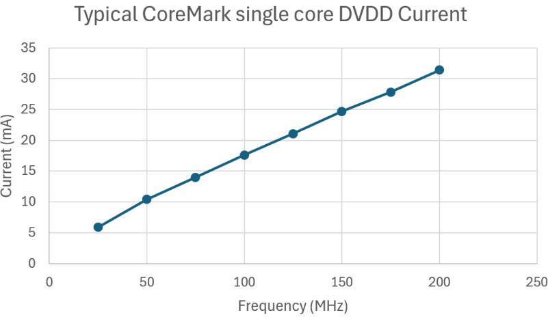
Typical CoreMark single core DVDD Current
The graph illustrates the relationship between the DVDD current and the core frequency of a typical RP2350 device while running the CoreMark benchmark. The x-axis represents Frequency in MHz, ranging from 0 to 250. The y-axis represents Current in mA, ranging from 0 to 35. The data points show a linear increase in current as frequency increases.
| Frequency (MHz) | Current (mA) |
|---|---|
| 25 | 6 |
| 50 | 10 |
| 75 | 14 |
| 100 | 17 |
| 125 | 21 |
| 150 | 24 |
| 175 | 27 |
| 200 | 31 |
Appendix A: Register field types
Changes from RP2040
Register field types are unchanged.
Standard types
RW:
- • Read/Write
- • Read operation returns the register value
- • Write operation updates the register value
RO:
- • Read-only
- • Read operation returns the register value
- • Write operations are ignored
WO:
- • Write-only
- • Read operation returns 0
- • Write operation updates the register value
Clear types
SC:
- • Self-Clearing
- • Writing a 1 to a bit in an SC field will trigger an event, once the event is triggered the bit clears automatically
- • Writing a 0 to a bit in an SC field does nothing
WC:
- • Write-Clear
- • Writing a 1 to a bit in a WC field will write that bit to 0
- • Writing a 0 to a bit in a WC field does nothing
- • Read operation returns the register value
FIFO types
These fields are used for reading and writing data to and from FIFOs. Accompanying registers provide FIFO control and status. There is no fixed format for the control and status registers, as they are specific to each FIFO interface.
RWF:
- • Read/Write FIFO
- • Reading this field returns data from a FIFO
- ◦ When the read is complete, the data value is removed from the FIFO
- ◦ If the FIFO is empty, a default value will be returned; the default value is specific to each FIFO interface
- • Data written to this field is pushed to a FIFO, Behaviour when the FIFO is full is specific to each FIFO interface
- • Read and write operations may access different FIFOs
RF:
- • Read FIFO
- • Functions the same as RWF, but read-only
WF:
- • Write FIFO
- • Functions the same as RWF, but write-only
Appendix B: Units used in this document
This datasheet follows standard practice for use of SI units as recommended by NIST, except in the context of memory and storage capacity. Here it adopts the convention that the prefixes k ( kilo ), M ( mega ) and G ( giga ) always refer to the nearest power of two to their standard decimal value. This aligns the datasheet with common usage for these units.
Memory and storage capacity
This datasheet expresses memory and storage capacity using the following units:
- • b: bit
- ◦ kb: kilobit, \( 2^{10} \text{ b} = 1024 \text{ b} \)
- ◦ Mb: megabit, \( 2^{20} \text{ b} = 1,048,576 \text{ b} \)
- ◦ Gb: gigabit, \( 2^{30} \text{ b} = 1,073,741,824 \text{ b} \)
- • B: byte, eight bits, one octet
- ◦ kB: kilobyte, \( 2^{10} \text{ B} = 1024 \text{ B} \)
- ◦ MB: megabyte, \( 2^{20} \text{ B} = 1,048,576 \text{ B} \)
- ◦ GB: gigabyte, \( 2^{30} \text{ B} = 1,073,741,824 \text{ B} \)
The bit is the most basic unit of information. A bit is either true (1) or false (0).
Transfer Rate
Units for transfer rate are dimensionally the product of one byte or bit with a unit of frequency such as MHz. Therefore the standard SI prefixes apply:
- • b/s: bit per second
- ◦ kb/s: kilobit per second, 1000 b/s
- ◦ Mb/s: megabit per second, 1,000,000 b/s
- ◦ Gb/s: gigabit per second, 1,000,000,000 b/s
- • B/s: byte per second, 8 b/s
- ◦ kB/s: kilobyte per second, 1000 B/s
- ◦ MB/s: megabyte per second, 1,000,000 B/s
- ◦ GB/s: gigabyte per second, 1,000,000,000 B/s
Physical Quantities
The following units express physical quantities such as voltage and frequency:
- • A: ampere, unit of electrical current, one coulomb per second
- ◦ mA: milliampere, \( 10^{-3} \) A
- ◦ \( \mu \) A: microampere, \( 10^{-6} \) A
- •
\(
\Omega
\)
: ohm, unit of electrical impedance or resistance, one volt per ampere
- ◦ M \( \Omega \) : megohm, \( 10^6 \) \( \Omega \)
- ◦ k \( \Omega \) : kilohm, \( 10^3 \) \( \Omega \)
- ◦ m \( \Omega \) : milliohm, \( 10^{-3} \) \( \Omega \)
- • V: volt, unit of electrical potential difference, one joule per coulomb
- ◦ kV: kilovolt, \( 10^3 \) V
- ◦ mV: millivolt, \( 10^{-3} \) V
- ◦ \( \mu \) V: microvolt, \( 10^{-6} \) V
- • Hz: hertz, unit of frequency, one period per second (
\(
s^{-1}
\)
)
- ◦ kHz: kilohertz, \( 10^3 \) Hz
- ◦ MHz: megahertz, \( 10^6 \) Hz
- ◦ GHz: gigahertz, \( 10^9 \) Hz
- • F: farad, unit of electrical capacitance, one coulomb per volt
- ◦ mF: millifarad, \( 10^{-3} \) F
- ◦ \( \mu \) F: microfarad, \( 10^{-6} \) F
- ◦ nF: nanofarad, \( 10^{-9} \) F
- ◦ pF: picofarad, \( 10^{-12} \) F
- • H: henry, unit of electrical inductance, one volt-second per ampere (
\(
VsA^{-1}
\)
)
- ◦ mH: millihenry, \( 10^{-3} \) H
- ◦ \( \mu \) H: microhenry, \( 10^{-6} \) H
- ◦ nH: nanohenry, \( 10^{-9} \) H
- • s: second, unit of time
- ◦ ms: millisecond, \( 10^{-3} \) s
- ◦ \( \mu \) s: microsecond, \( 10^{-6} \) s
- ◦ ns: nanosecond, \( 10^{-9} \) s
- ◦ ps: picosecond, \( 10^{-12} \) s
- • J: joule, unit of energy or work, one newton-metre
- • C: coulomb, unit of electrical charge
- ◦ mC: millicoulomb, \( 10^{-3} \) C
- ◦ \( \mu \) C: microcoulomb, \( 10^{-6} \) C
- ◦ nC: nanocoulomb, \( 10^{-9} \) C
- • m: metre, unit of length or distance
- ◦ mm: millimetre, \( 10^{-3} \) m
- • \( ^{\circ}C \) : degree celsius, unit of temperature
- • W: watt, unit of power, one joule per second ( \( Js^{-1} \) ) or one volt-ampere (VA)
- ◦ mW: milliwatt, \( 10^{-3} \) W
- ◦ \( \mu \) W: microwatt, \( 10^{-6} \) W
- ◦ nW: nanowatt, \( 10^{-9} \) W
Scale Prefixes
The standard SI prefixes used in the previous sections are:
- • G: giga, factor of \( 10^9 \) (one short billion)
- • M: mega, factor of \( 10^6 \) (one million)
- • k: kilo, factor of \( 10^3 \) (one thousand)
- • c: centi, factor of \( 10^{-2} \) (one hundredth)
- • m: milli, factor of \( 10^{-3} \) (one thousandth)
- • \( \mu \) , micro, factor of \( 10^{-6} \) (one millionth)
- • n: nano, factor of \( 10^{-9} \) (one short billionth)
- • p: pico, factor of \( 10^{-12} \) (one short trillionth)
The customary binary prefixes used in the memory and storage capacity section are:
- • G: giga, factor of \( 2^{30} \) (approximately \( 10^9 \) )
- • M: mega, factor of \( 2^{20} \) (approximately \( 10^6 \) )
- • k: kilo, factor of \( 2^{10} \) (approximately \( 10^3 \) )
These customary binary prefixes are equivalent to the following prefixes from IEC 60027-2:
- • Gi, gibi
- • Mi, mebi
- • Ki, kibi
Digit Separators
Numbers written out with many digits may have either commas or spaces inserted for easier reading:
- • 1,000,000: one million
- • 1 000 000: one million
A comma in a number never represents a decimal (radix) point.
Appendix C: Hardware revision history
This appendix summarises the differences between RP2350 hardware revisions, referred to as
steppings
. To determine the stepping of an unknown device, check the package markings, as described in
Section 14.4
. Software running on the device can also read the
CHIP_ID.REVISION
register field, or call the
rp2350_chip_version()
SDK function.
In this appendix:
- • The term fix refers to an issue that's fully resolved.
- • The term mitigate refers to an issue that's either partially resolved or believed to be fully resolved but with an unpredictable underlying cause, such as a fault injection vulnerability.
- • The term update refers to any other difference between steppings.
This appendix offers a high-level overview; for detailed information, refer to individual errata entries in appendix E.
RP2350 A2
Stepping A2 is identified by a
CHIP_ID.REVISION
value of
0x2
.
A2 is the first generally available version of RP2350, and the earliest stepping documented in this datasheet.
RP2350 A3
Stepping A3 is identified by a
CHIP_ID.REVISION
value of
0x3
.
Hardware changes
Stepping A3 introduces the following hardware fixes and mitigations:
- • Fix RP2350-E3 : in QFN-60 package, GPIO_NS_MASK controls wrong PADS registers. Hardware now remaps GPIO_NS_MASK to the correct PADS registers in the QFN60 package.
- • Fix RP2350-E9 : increased leakage current on Bank 0 GPIO when pad input is enabled. The pad circuit is modified to eliminate the erroneous leakage path through the input buffer.
- • Mitigate RP2350-E12 : inadequate synchronisation of USB status signals. Signals used by the bootrom are now valid across the full PVT range in the bootrom's clock configuration. Other software must not rely on these mitigations.
- •
Mitigate
RP2350-E16
:
USB_OTP_VDD
disruption can cause corrupt OTP row read data. The following changes apply:
- ◦ Multiple changes to the OTP PSM and OTP read circuits to detect unreliable operation.
- ◦ RISC-V debug is now disabled by CRIT1.SECURE_DEBUG_DISABLE , in addition to CRIT1.DEBUG_DISABLE . (On A2, only the latter bit was used.)
- ◦ CRIT0.ARM_DISABLE no longer disables the Arm processors.
- ◦ Programming both CRIT0.ARM_DISABLE and CRIT0.RISCV_DISABLE is decoded as an illegal combination, and the device won't boot.
- •
Update
the reset state of the following clock configuration registers:
- ◦ ROSC:
FREQA.DS0_RANDOMandFREQA.DS1_RANDOMfrom 0 to 1, enabling randomisation of first two drive stages. - ◦ CLOCKS:
CLK_SYS_CTRL.SRCfrom 0 to 1 (select AUX source). - ◦ CLOCKS:
CLK_SYS_CTRL.AUXSRCfrom 0 to 2 (select ROSC as AUX source).
- ◦ ROSC:
Bootrom changes
The A3 bootrom introduces the following changes:
- •
Fix RP2350-E10:
UF2 drag-and-drop doesn't work with partition tables. This previously required a workaround in
picotool, but the A3 bootrom no longer requires this workaround.picotoolretains the workaround for compatibility with A2. - •
Fix RP2350-E13:
a binary containing an explicitly invalid
IMAGE_DEFfollowed by a validIMAGE_DEF(in that order) fails to boot. - •
Fix RP2350-E14:
the bootrom
connect_internal_flash()function always uses pin 0, ignoring any configuredFLASH_DEVINFOCS1 chip select pin. - •
Fix RP2350-E15:
the bootrom
otp_access()function applies incorrect access permission to pages 62 and 63. - •
Fix RP2350-E19:
RP2350 reboot halts if certain bits are set in
FRCE_OFFwhen rebooting. - •
Mitigate RP2350-E20:
an attacker with physical access to the chip and the ability to physically glitch the CPU at precise times could cause unsigned code execution on a secured RP2350 by targeting legitimate Non-secure calls to the bootrom
reboot()function. - • Mitigate RP2350-E21: an attacker with physical access to the chip and the ability to physically glitch the CPU at precise times, could extract sensitive data from OTP on a RP2350 in BOOTSEL mode.
- •
Fix RP2350-E22:
parsing a malformed lollipop
block loopcauses the system to halt rather than fail. - •
Fix RP2350-E23:
PICOBOOT
GET_INFOcommand always returns zero forPACKAGE_SEL - • Mitigate RP2350-E26: RCP random delays can create a side-channel. These delays are disabled in the bootrom.
- •
Update
the early boot path to change the
clk_refdivider from 1 to 5, and the ROSC divider from 8 to 2.- ◦ Together with the register reset state changes, this increases the boot
clk_sysfrequency by a factor of 4, to approximately 48 MHz. - ◦ These changes reduce boot time and fault injection susceptibility.
- ◦ These changes apply for all boot outcomes, including watchdog and POWMAN vector boot.
- ◦ Together with the register reset state changes, this increases the boot
RP2350 A4
Stepping A4 is identified by a
CHIP_ID.REVISION
value of 0x8.
Hardware Changes
This stepping has no hardware changes.
Bootrom Changes
The A4 bootrom introduces the following changes:
- • Fix RP2350-E18: the RP2350 forever fails to boot if FLASH_PARTITION_SLOT_SIZE contains an invalid ECC bit pattern. This issue is a consequence of RP2350-E17 (a guarded read on a single ECC OTP row causes a fault if the data in the adjacent row isn't also valid ECC data). The underlying hardware issue isn't resolved, but the bootrom avoids the issue in this instance.
- • Mitigate RP2350-E24: an attacker with physical access to the chip, moderate hardware, and the ability to physically glitch the CPU at precise times, could cause unsigned code execution on a secured RP2350. The A4 bootrom contains additional fault injection mitigations for this vulnerability, and for other potential vulnerabilities with the same underlying mechanism.
- • Fix RP2350-E25: a LOAD_MAP that uses non-word sizes previously didn't cause an error. The bootrom now correctly rejects these structures.
Appendix E: Errata
Alphabetical by section.
ACCESSCTRL
RP2350-E3
| Reference | RP2350-E3 |
| Summary | In QFN-60 package,
GPIO_NS_MASK
controls wrong
PADS
registers |
| Affects | RP2350 A2, QFN-60 package only |
| Description | RP2350 remaps IOs, their control registers and their ADC channels so that both package sizes appear to have consecutively numbered GPIOs, even though for physical design reasons the QFN-60 package bonds out a sparse selection of IO pads. The connection between the
This means that granting Non-secure access to the
The QSPI
|
| Workaround | Disable Non-secure access to the
Implement a Secure Gateway (Arm) or
|
| Fixed by | RP2350 A3, Documentation, Software |
Bootrom
RP2350-E10
| Reference | RP2350-E10 |
| Summary | UF2 drag-and-drop doesn't work with partition tables |
| Affects | RP2350 A2 |
| Description | When dragging and dropping a UF2 onto the USB Mass Storage Device, the bootrom on chip revision A2 doesn't set up the flash before checking the partition table. This causes the UF2 download to fail if there is a partition table present. |
| Workaround | Add a single block at the start of the UF2 with an Absolute family ID, targeting the end of Flash, with block number set to 0 and number of blocks set to 2. This block is written to flash first but doesn't reboot the device, and sets up the flash for the rest of the UF2 to be downloaded correctly. This is handled for you automatically by
This workaround means that the last block of flash is erased when downloading such a UF2, which could overwrite user data. As of
|
| Fixed by | RP2350 A3 bootrom, Documentation, Software |
RP2350-E13
| Reference | RP2350-E13 |
| Summary | A binary containing an
explicitly invalid
IMAGE_DEF
followed by a valid
IMAGE_DEF
(in that order) fails to boot |
| Affects | RP2350 A2 |
| Description | When the block loop of a binary contains an
An
|
| Workaround | Instead of an
explicitly invalid
SDK uses this workaround for RP2040 binaries. When you set
|
| Fixed by | RP2350 A3 bootrom, Documentation, Software |
RP2350-E14
| Reference | RP2350-E14 |
| Summary | The bootrom
connect_internal_flash()
function always uses pin 0, ignoring any configured
FLASH_DEVINFO
CS1 chip select pin |
| Affects | RP2350 A2 |
| Description | When using the bootrom function connect_internal_flash() to configure CS1 (for instance, during a flash boot), the bootrom always configures the pad registers for pin 0, ignoring any CS1 pin specified in FLASH_DEVINFO . As a result, the specified CS1 pin remains isolated (see Section 9.7 ). Accesses to the QSPI device connected to the second chip select fails unless CS1 is connected to pin 0. FLASH_DEVINFO can be configured in OTP or at runtime. For more information, see flash_devinfo16_ptr . |
| Workaround | Manually configure the CS1 pads registers to remove the isolation after using the bootrom connect_internal_flash() function. Alternatively, connect CS1 to pin 0. |
| Fixed by | RP2350 A3 bootrom, Documentation, Software |
RP2350-E15
| Reference | RP2350-E15 |
| Summary | The bootrom otp_access() function applies incorrect access permission to pages 62 & 63 |
| Affects | RP2350 A2 |
| Description | The bootrom otp_access() function incorrectly applies the access permissions specified in OTP rows PAGE62_LOCK1 and PAGE63_LOCK1 to the entirety of their respective OTP pages (62 and 63). This is incorrect, as pages 62 and 63 contain lock words for other pages: each lock word is instead protected by the permissions of the corresponding page. The ATE programming then locks down write access from non-Secure software and the bootloader to the page 63 lock word (to prevent non-Secure setting of the RMA flag), and write access from non-Secure software to the page 62 lock word. This prevents non-Secure software from modifying any of the OTP page locks, and the bootloader from modifying the locks for pages 32-63. |
| Workaround | When running code on the device, don't use the non-Secure otp_access() function to set locks for OTP pages. To set OTP page locks from non-Secure code, implement your own Secure API to do this that can be called from non-Secure code. Page locks for OTP pages 32-63 can be set by picotool using the picotool otp permissions command. This command loads a Secure binary into XIP SRAM on the device to change the permissions before rebooting back into the USB bootloader. |
| Fixed by | RP2350 A3 bootrom, Documentation, Software |
RP2350-E18
| Reference | RP2350-E18 |
| Summary | The RP2350 will forever fail to boot if FLASH_PARTITION_SLOT_SIZE contains an invalid ECC bit pattern |
| Affects | RP2350 A2, RP2350 A3 |
| Description | If ECC row programming is interrupted, an ECC row may contain a value that fails ECC validation. Because any ECC could potentially contain an invalid, partially written value, the bootrom uses a separate "enable" flag in OTP to indicate whether a particular ECC row is expected to contain a valid value. The user is expected to only set this flag after a particular ECC row is known to have been written correctly. For
In the case of
|
| Workaround | Don't program
FLASH_PARTITION_SLOT_SIZE
or at least be aware that doing so may brick your device if the programming operation is interrupted or fails. |
| Fixed by | RP2350 A4 bootrom, Documentation |
RP2350-E19
| Reference | RP2350-E19 |
| Summary | RP2350 reboot hangs if certain bits are set in
FRCE_OFF
when rebooting. |
| Affects | RP2350 A2 |
| Description | An incorrect assertion in the boot path, assumes the all bits (other than
FRCE_OFF.PROC1
) are clear. These bits can only be set during boot if the user had set them and then re-entered the boot path. |
| Workaround | Don't perform a
WATCHDOG
or
POWMAN
boot, or a core0 reset with bits other than
FRCE_OFF.PROC1
set. |
| Fixed by | RP2350 A3 bootrom, Documentation |
RP2350-E20
| Reference | RP2350-E20 |
| Summary | An attacker with physical access to the chip and the ability to physically "glitch" the CPU at precise times, could cause unsigned code execution on a secured RP2350 by targeting legitimate Non-secure calls to the bootrom
reboot()
function |
| Affects | RP2350 A2 |
| Description | The RP2350 bootrom provides a
A particular reboot type (
|
| Workaround | If any WATCHDOG based reboot types other than into the regular boot path aren't required (this includes programmatic reboots into BOOTSEL mode and FLASH_UPDATE boots which are important when using A/B partitions), the OTP flag BOOT_FLAGS0.DISABLE_WATCHDOG_SCRATCH can be set, which causes the WATCHDOG scratch registers to be completely ignored during boot, meaning that the only type of boot available via WATCHDOG reset is regular boot. A more refined approach would be to disable use of the reboot() function from Non-secure code. This is the default case for Non-secure code started by a secure application (see Section 5.4.2 ). However, the BOOTSEL mode bootloader is itself a Non-secure application that does have access to the function. BOOTSEL mode, however, can be disabled if not needed through BOOT_FLAGS0.DISABLE_BOOTSEL_UART_BOOT , BOOT_FLAGS0.DISABLE_BOOTSEL_USB_PICOB00T_IFC , and BOOT_FLAGS0.DISABLE_BOOTSEL_USB_MSD_IFC . BOOT_FLAGS0.DISABLE_BOOTSEL_USB_PICOB00T_IFC is the most important because PICOB00T provides a conduit for a user to pass specific parameters to the bootrom reboot() function. However, any other use of BOOTSEL mode could be vulnerable in conjunction with some other future attack on the Non-secure code. |
| Credit | Marius Muench |
| Fixed by | RP2350 A3 bootrom, Documentation |
RP2350-E21
| Reference | RP2350-E21 |
| Summary | An attacker with physical access to the chip, and the ability to physically "glitch" the CPU at precise times, could potentially extract sensitive data from OTP on a RP2350 in BOOTSEL mode. |
| Affects | RP2350 A2 |
| Description | An attacker with physical access to the chip, could precisely time physical glitch attacks during entry to BOOTSEL mode and cause some OTP page access permissions for BOOTSEL mode not to be applied, leading to possible exposure of sensitive data. The RP2350 BOOTSEL mode exposes an API over PICOB00T such that a user can read or write OTP rows through picotool . Certain OTP rows (such as encryption keys or other secrets) shouldn't be readable through this method. Equally, certain rows might be protected against writes. This is handled at the page (64 row) level by page locks stored in OTP. On entry to BOOTSEL mode, the OTP should be locked down such that no software (including Secure software) can access anything not marked as accessible to BOOTSEL mode. However, with two precisely timed processor glitches, it's possible to prevent a page being correctly locked. |
| Workaround |
BOOT_FLAGS0.DISABLE_BOOTSEL_USB_PICOB00T_IFC is the most important, as PICOB00T provides the conduit for a user to access the OTP, however any other use of BOOTSEL mode could be vulnerable in conjunction with some other future attack on the non-Secure code.
|
| Credit | Thomas Roth |
| Fixed by | RP2350 A3 bootrom, Documentation |
RP2350-E22
| Reference | RP2350-E22 |
| Summary | Parsing a malformed "lollipop" block loop will cause a hang rather than a failure |
| Affects | RP2350 A2 |
| Description | PARTITION_TABLES and IMAGE_DEFS metadata are stored as part of a block loop. These block loops are parsed during boot and at other times. A "lollipop" block loop is an invalid block loop, which loops back from the last block to a block, which isn't the first. Such an invalid block loop is never generated by the SDK or by picotool ; however, it could potentially be generated by other tooling. |
| Workaround | Don't use "lollipop" block loops. If you program a "lollipop" block loop into flash such that it's read during the boot process, it will cause a boot hang and also a hang on entry into BOOTSEL mode. Therefore, to re-enable booting, you must clear the flash in some other way, for example, from the debugger over SWD. |
| Fixed by | RP2350 A3 bootrom, Documentation |
RP2350-E23
| Reference | RP2350-E23 |
| Summary | PICOBOT GET_INFO command always returns zero for PACKAGE_SEL |
| Affects | RP2350 A2 |
| Description | The PICOBOT GET_INFO command can be used to get system information in a similar way to the bootrom get_sys_info() function. This information can include the value read from PACKAGE_SEL , which indicates whether the RP2350 package is QFN60 or QFN80. The SYSINFO block is erroneously left in reset when entering BOOTSEL mode, and thus this register is read as zero when accessed via PICOBOT. This problem doesn't affect use of the bootrom get_sys_info() function itself from user code. |
| Workaround | Determine the package size by reading register_link_macro:[register=OTP_DATA_NUM_GPIOS_ROW] via the PICOBOT OTP_READ command instead. This workaround is used by picotool . |
| Fixed by | RP2350 A3 bootrom, Documentation, Software |
RP2350-E24
| Reference | RP2350-E24 |
| Summary | An attacker with physical access to the chip, moderate hardware, and the ability to physically "glitch" the CPU at precise times, could cause unsigned code execution on a secured RP2350. |
| Affects | RP2350 A2, RP2350 A3 |
| Description | An attacker with physical access to the chip, and the ability to switch the contents of "flash" as read by the RP2350 over QSPI during boot at precise times, could, combined with a precisely-timed physical "glitch" attack of the CPU, trick the bootrom into checking the signature of data other than the program binary as loaded into memory during secure boot. If this "other" data passes the signature check, then the attacker's binary is executed without itself having passed a signature check, which allows the user to run arbitrary unsigned code on the RP2350. |
| Credit | Kévin Courdresses (see https://courk.cc/rp2350-challenge-laser#flash-memory-organization ) |
| Workaround | None |
| Fixed by | RP2350 A4 bootrom |
RP2350-E25
| Reference | RP2350-E25 |
| Summary | A LOAD_MAP that uses non-word sizes doesn't cause an error. |
| Affects | RP2350 A2, RP2350 A3 |
| Description | Non-word sizes in a LOAD_MAP aren't supported and were documented as such. However, they don't currently cause an error. Whilst non-word sizes might currently work in some certain cases, you should never use them because they might not work as you expect in all cases and can be properly treated as an error in the future. The SDK and picotool don't generate such LOAD_MAPs with non-word sized entries. |
| Workaround | Don't use non-word (not multiple of 4) sizes in a LOAD_MAP . A best practice is to make sure that linker memory segments are both word-sized and word-aligned. As of the RP2350 A4 bootrom, non-word sizes are detected when checking the LOAD_MAP and cause the IMAGE_DEF to be considered invalid if present. |
| Fixed by | RP2350 A4 bootrom, Documentation |
Bus Fabric
RP2350-E27
| Reference | RP2350-E27 |
| Summary | Bus priority controls apply to wrong managers for APB and FASTPERI arbiters. |
| Affects | RP2350 A2, RP2350 A3, RP2350 A4 |
| Description | RP2350 bus fabric consists mainly of an AHB5 crossbar, where 6 upstream ports (managers) are routed to 15 downstream crossbar ports. Figure 5 shows the overall structure of the bus fabric, including this crossbar. Because there can be multiple accesses to a given downstream crossbar port on any one cycle, an arbiter circuit selects one transfer to forward to the downstream port, and stalls all other transfers targeting this port. The BUSCTRL BUS_PRIORITY register controls these arbiter circuits. It configures a 1-bit priority level for each of the following four groups of AHB5 managers:
Accesses from high-priority managers are always routed preferentially over those from low-priority managers. Multiple accesses from managers of the same priority are processed one at a time, taking turns in a repeating cycle (round-robin arbitration). On the FASTPERI and APB arbiters, these signals are mis-wired, such that the wrong managers are prioritised:
The BUS_PRIORITY controls are applied correctly for all other arbiters: ROM, SRAM, and XIP. For example, if the DMA_R and DMA_W bits were set, this would prioritise DMA over processor access to ROM, SRAM, and XIP. However, peripheral access would prioritise DMA read and core 1 load/store over DMA write and core 0 load/store. |
| Workaround | There is no complete fix, but the necessary prioritisation can often still be achieved by configuring BUS_PRIORITY for correct priority at the peripherals, and then arranging buffers in SRAM to minimise contention, such as using SRAM8 or SRAM9 as processor-private memories. Also consider the following approaches:
|
| Fixed by | Documentation |
DMA
RP2350-E5
| Reference | RP2350-E5 |
| Summary | Interactions between CHAIN_TO and ABORT of active channels |
| Affects | RP2350 A2, RP2350 A3, RP2350 A4 |
| Description | The CHAN_ABORT register commands a DMA channel to stop issuing transfers, and to clear its BUSY flag once in-flight transfers have completed. This was originally intended for recovering channels that are stuck with their DREQ low. An ABORT is initiated by writing a bitmap of aborted channels to CHAN_ABORT . Bits remain set until each channel comes to rest. This erratum is a compound of two behaviours: first, aborting a channel will cause its CHAIN_TO to fire, if and only if the aborted channel is the last channel to have completed a write transfer. Second, a channel undergoing an ABORT is susceptible to be re-triggered on the last cycle before the ABORT register clears, because the channel is both inactive and enabled on this cycle, and the ABORT itself doesn't inhibit triggering. However, since the ABORT is still in effect, the transfer count is held at zero. On the cycle after the ABORT finishes, the channel completes because its transfer counter is zero. This causes the channel's IRQ and CHAIN_TO to fire on the cycle after the ABORT completes. These two behaviours are problematic when aborting multiple channels that chain to one another, since they may cause the channels to immediately restart post-abort. |
| Workaround | Before aborting an active channel, clear the EN bit ( CH0_CTRL_TRIG.EN ) of both the aborted channel and any channel it chains to. This ensures the channel isn't susceptible to re-triggering. |
| Fixed by | Documentation |
RP2350-E8
| Reference | RP2350-E8 |
| Summary | CHAIN_TO might not fire for zero-length transfers |
| Affects | RP2350 A2, RP2350 A3, RP2350 A4 |
| Description | The CTRL.CHAIN_TO field configures a channel to start another channel once it completes its programmed sequence of transfers. The CHAIN_TO takes place on the cycle where the channel's last write completes, and the chaine becomes active on the next cycle. The hardware implementation assumes that CHAIN_TO always happens as a result of a write completion. This isn't the case when a channel is triggered with a transfer count of zero; in this case the channel completes on the cycle immediately after the trigger without performing any bus accesses. A CHAIN_TO from a channel started with a transfer count of zero will fire if and only if that channel is the last channel to have completed a write transfer. This is true only when the channel in question has previously performed a non-zero-length sequence of transfers, and no other channel has completed a write since. |
| Workaround | Don't use CHAIN_TO in conjunction with zero-length transfers. Avoid zero-length transfers in the middle of control block lists, and replace them with dummy transfers if possible. |
| Fixed by | Documentation |
GPIO
RP2350-E9
| Reference | RP2350-E9 |
| Summary | Increased leakage current on Bank 0 GPIO when pad input is enabled |
| Affects | RP2350 A2 |
| Description | For GPIO pads 0 through 47: Increased leakage current when Bank 0 GPIO pads are configured as inputs and the pad is somewhere between \( V_{IL} \) and \( V_{IH} \) (the undefined logic region). When the pad is set as an input (input enable is enabled and output enable is disabled) and the voltage on the pad is within the undefined logic region, the leakage current exceeds the standard specified \( I_{IN} \) leakage level. During this condition the pad can source current (the exact amount is dependent on the chip itself and the exact pad voltage, but typically around 120µA). This leakage will hold the pad at around 2.2 V as that is the effective source voltage of the leakage, and can only be overcome with a suitably low impedance driver / pull. The pad pull-down (if enabled) is significantly weaker than the leakage current in this state and therefore isn't strong enough to pull the pad voltage low. Driving / pulling the pad input low with a low impedance source of 8.2 kΩ or less will overcome the erroneous leakage and drive the voltage below the level where the leakage current occurs, so in this case if the pad is driven / pulled low it will stay low. The erroneous leakage only occurs (and continues to occur) when the pad input enable is enabled; disabling the input enable will reset (remove) the leakage. The pad pull-up still works. If enabled it will pull the pad to IOVDD as it will pull the input voltage out of the problematic range. The voltages and currents above are based on IOVDD at 3.3 V. For IOVDD at 1.8 V the effective source voltage of the leakage becomes 1.8 V and the peak current is around 30µA. This is effectively a pull-up (separate to the standard pad pull-up) when the pad voltage is between 0.6 V and 1.8 V. These graphs show the leakage current versus pad input voltage for a typical chip for IOVDD at 3.3 V Figure 153 and 1.8 V Figure 154 . In detail, this issue presents under the following conditions, for any GPIO 0 through 47:
When all of the above conditions are met, the input leakage of the pad may exceed the specification. This issue may affect a number of common circuits:
If the internal pull-up is enabled then any floating signal will be pulled high thus removing increased leakage condition as the excess leakage is only sourcing current. This of course can't prevent the increased leakage if the pad is fed via a strong source e.g. strong potential divider. This doesn't affect the pull-down behaviour of the pads immediately following a PoR or RUN reset because the input enable field is initially clear. The pull-down resistor functions normally in this state. This issue doesn't affect the QSPI pads, which use a different pad macro without the faulty circuitry. The USB PHY's pins are also unaffected. This issue does also affect the SWD pads, which use the same fault-tolerant pad macro as the Bank 0 GPIOs. However, both SWD pads are pull-up by default, so there is no ill effect. |
| Workaround | If pad pull-down behaviour is required, clear the pad input enable in GPIO0.IE (for GPIOs 0 through 47) to ensure that the pad pull-down resistor pulls the pad signal low. To read the state of a pad pulled-down GPIO from software, enable the input buffer by setting GPIO0.IE immediately before reading, and then re-disable immediately afterwards. If the pad is already a logic-0, re-enabling the input doesn't disturb the pull-down state. Alternatively an external pull-down of 8.2 kΩ or less can be used. PIO programs can't toggle pad controls and therefore external pulls may be required, depending on your application. As normal, if ADC channels are being used on a pin, clear the relevant GPIO input enable as stated in Section 12.4.3 . |
| Fixed by | RP2350 A3, Documentation |
Figure 153. GPIO Pad leakage for IOVDD=3.3 V
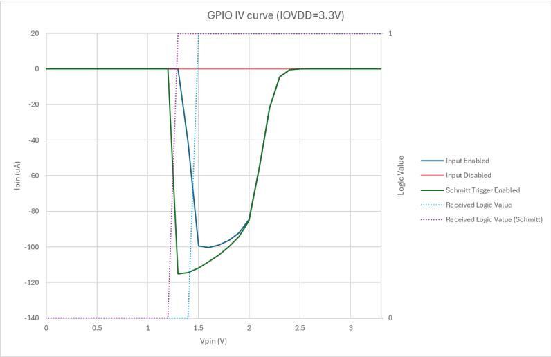
The graph shows the input current (I pin ) in microamperes (μA) on the y-axis (ranging from -140 to 20) versus the input voltage (V pin ) in Volts (V) on the x-axis (ranging from 0 to 3.5). The title is "GPIO IV curve (IOVDD=3.3V)". The legend indicates five data series: "Input Enabled" (solid blue line), "Input Disabled" (solid red line), "Schmitt Trigger Enabled" (solid green line), "Received Logic Value" (dotted blue line), and "Received Logic Value (Schmitt)" (dotted green line). The "Input Enabled" curve shows a sharp drop to approximately -110 μA at V pin ≈ 1.4 V, then rises to 0 μA at V pin ≈ 2.4 V. The "Schmitt Trigger Enabled" curve shows a similar but less steep drop, reaching a minimum of about -120 μA at V pin ≈ 1.4 V. The "Received Logic Value" and "Received Logic Value (Schmitt)" curves are step functions that transition from 0 to 1 at V pin ≈ 1.4 V.
Figure 154. GPIO Pad leakage for IOVDD=1.8 V
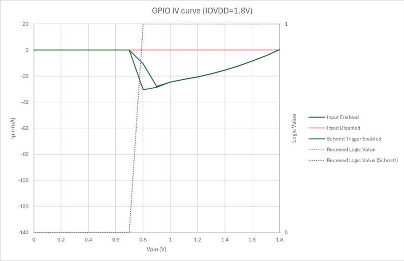
The graph shows the input current (I pin ) in microamperes (μA) on the y-axis (ranging from -140 to 20) versus the input voltage (V pin ) in Volts (V) on the x-axis (ranging from 0 to 1.8). The title is "GPIO IV curve (IOVDD=1.8V)". The legend is the same as in Figure 153. The "Input Enabled" curve shows a sharp drop to approximately -30 μA at V pin ≈ 0.7 V, then rises to 0 μA at V pin ≈ 1.8 V. The "Schmitt Trigger Enabled" curve shows a similar but less steep drop, reaching a minimum of about -35 μA at V pin ≈ 0.7 V. The "Received Logic Value" and "Received Logic Value (Schmitt)" curves are step functions that transition from 0 to 1 at V pin ≈ 0.7 V.
Hazard3
RP2350-E4
| Reference | RP2350-E4 |
| Summary | System Bus Access stalls indefinitely when core 1 is in clock-gated sleep |
| Affects | RP2350 A2, RP2350 A3, RP2350 A4 |
| Description | System Bus Access (SBA) is a RISC-V debug feature that allows the Debug Module direct access to the system bus, independent of the state of harts in the system. RP2350 implements SBA by arbitrating Debug Module bus accesses with the core 1 load/store port. Hazard3 implements custom low-power states controlled by the MSLEEP CSR. When MSLEEP .DEEPSLEEP is set, Hazard3 completely gates its clock, with the exception of the minimal logic required to wake again. Due to a design oversight, this also clock-gates the arbiter between SBA and load/store bus access. (This is addressed in upstream commit c11581e .) Consequently, if you initiate an SBA transfer whilst MSLEEP .DEEPSLEEP is set on core 1, and core 1 is in a WFI-equivalent sleep state, the SBA transfer will make no progress until core 1 wakes from the WFI state. The processor wakes upon an enabled interrupt being asserted, or a debug halt request. |
| Workaround | Either configure your debug translator to not use SBA, or don't enter clock-gated sleep on core 1. The A2 bootrom mitigates this issue by not setting DEEPSLEEP in the initial core 1 wait-for-launch code. The processors are synthesised with hierarchical clock gating, so the top-level clock gate controlled by the DEEPSLEEP flag brings minimal power savings over a default WFI sleep state. |
| Fixed by | Documentation |
RP2350-E6
| Reference | RP2350-E6 |
| Summary | PMPCFGx RWX fields are transposed |
| Affects | RP2350 A2, RP2350 A3, RP2350 A4 |
| Description | The Physical Memory Protection unit (PMP) defines read, write and execute permissions (RWX) for configurable ranges of physical memory. The RWX permissions for four regions are packed into each 32-bit PMPCFG register, PMPCFG0 through PMPCFG3 . Per the RISC-V privileged ISA specification, the permission fields are ordered X, W, R from MSB to LSB. Hazard3 implements them in the order R, W, X. This means software using the correct bit order will have its read permissions applied as execute, and vice versa. (See upstream commit 7d37029 .) |
| Workaround | When configuring PMP with X != R, use the bit order implemented by this version of Hazard3. In the SDK, the hardware/regs/rvcsr.h register header provides bitfield definitions for the as-implemented order when building for RP2350. |
| Fixed by | Documentation |
RP2350-E7
| Reference | RP2350-E7 |
| Summary | U-mode doesn't ignore mstatus.mie |
| Affects | RP2350 A2, RP2350 A3, RP2350 A4 |
| Description | The
The RISC-V privileged ISA specification requires that the interrupt enable flag for a given privilege mode is treated as
Hazard3 doesn't implement this rule, so entering U-mode with M-mode interrupts disabled results in no M-mode interrupts being taken. (See upstream commit a84742a .) |
| Workaround | When returning to U-mode from M-mode via an
mret
with
mstatus.mpp == 0
, ensure
mstatus.mpie
is set, so that IRQs will be enabled by the return. |
| Fixed by | Documentation |
OTP
RP2350-E16
| Reference | RP2350-E16 |
| Summary | USB_OTP_VDD
disruption can result in corrupt OTP row read data |
| Affects | RP2350 A2 |
| Description | The OTP array has a read voltage generated from
The erroneous behaviour includes, but isn't limited to:
In the case of guarded reads, the first failure mode can result in the guard read check passing and the guard word also ending up as the read data. If the critical data are the
Guarded ECC reads aren't typically vulnerable to corruption of this nature as the guard word is an invalid ECC word, and bit deletion or byte shifting reliably invalidates the ECC check. RP2350 A3 incorporates more safeguards against erroneous OTP behaviour. If any of the following checks fail, the chip is reset back to the start of the OTP PSM stage.
These checks are performed regardless of the security state of the chip. The OTP regulator check may be masked with bit 2 of the
|
| Credit | Aedan Cullen (see https://github.com/aedancullen/hacking-the-rp2350 ) |
| Workaround | None |
| Fixed by | RP2350 A3 |
RP2350-E17
| Reference | RP2350-E17 |
| Summary | Performing a guarded read on a single ECC OTP row causes a fault if the data in the adjacent row isn't also valid ECC data. |
| Affects | RP2350 A2, RP2350 A3, RP2350 A4 |
| Description | Each "ECC row" in OTP stores 16 bits of user data along with error correction information used to correct and/or detect bit errors. ECC rows are used to store data value, which are written a full 16 bits at a time into OTP. A "guarded" ECC row read is intended to be used by the RP2350 boot path, or other Secure software when it expects to read an ECC row and can't proceed if the row value is invalid. Reading such an invalid ECC value through a "guarded" read halts the chip until it's rebooted. If ECC row programming is interrupted, an ECC row might contain a value that fails ECC validation. Because any ECC could potentially contain an invalid, partially written value, the bootrom uses a separate "enable" flag in OTP to indicate whether a particular ECC row is expected to contain a valid value. The user is expected to only set this flag after a particular ECC row is known to have been written correctly. The RP2350 OTP hardware actually reads a pair of rows (starting on the even row) whenever an ECC read is performed but only returns one row value. When performing a guarded ECC read, it actually checks both rows validity, so the guarded read can cause a halt if either row in the pair isn't a valid ECC value. |
| Workaround |
This workaround is fine for user use of OTP, however certain pre-existing ECC row pairs used by the bootrom violate workaround 2: To be absolutely safe, don't update and set the "enable" flag for one half of the pair after you have set the "enable" flag for the other half. If you want to set both ECC values safely, set them both, then set both "enable" flags. |
| Fixed by | Documentation |
RP2350-E28
| Reference | RP2350-E28 |
| Summary | OTP keys for pages 62/63 are applied to all lock words 0 through 63 |
| Affects | RP2350 A2, RP2350 A3, RP2350 A4 |
| Description | As described in Section 13.5 , the uppermost 64 words (128 rows) of OTP contain protection information for each 128-byte page of OTP. The total ECC data capacity of the OTP is \( 64 \times 128 \text{ B} = 8192 \text{ B} \) , so there is one such lock word for each page. The permissions in each lock word \( n \) cover OTP rows \( 64 * n \) through \( 64 * n + 63 \) (inclusive), and they also cover the lock word itself. This makes lock words 62 and 63 special because they don't have any associated OTP page. This is because those pages would overlap with the locations where the lock words are stored. Instead, lock words 62 and 63 should only protect themselves. This rule is applied correctly for the effects of LOCK_NS and LOCK_S bits. However, the protection checks for the KEY_R , KEY_W , and NO_KEY_STATE bits don't handle pages 62 and 63 correctly. Instead, they simply divide the row number by 64 to look up the lock word. The effect is that lock words 0 through 31 have a key protection state defined by PAGE62_LOCK0 , and lock words 32 through 63 have a key protection state defined by PAGE63_LOCK0 . Conversely, the key configuration in lock words 0 through 61 does not affect the accessibility of those lock words. It only affects the accessibility of the actual data pages protected by those lock words. |
| Workaround | As a partial mitigation, factory programming revokes Non-secure write permission to pages 62 and 63 on all devices. This avoids Non-secure software disabling Secure access to lock words by deliberately installing an invalid key. For the full list of permissions pre-programmed on blank devices, see Section 13.5.5 . This mitigation is applied on all versions of RP2350. Software shouldn't rely on OTP access keys for protection of lock words. |
| Fixed by | Documentation |
RCP
RP2350-E26
| Reference | RP2350-E26 |
| Summary | RCP random delays can create a side-channel |
| Affects | RP2350 A2, RP2350 A3, RP2350 A4 |
| Description | The RCP delay is implemented as a coprocessor stall; this has the effect of completely pausing the associated core. As the core is effectively halted for the duration of the delay, this represents a significant reduction in gate toggle activity across the chip if there are no other bus managers active (e.g. other CPU or DMA). The reduction in toggle activity causes a reduction in DVDD current, and the typical length of the delay means that the reduction is measureable outside of the chip. The reduction in current and subsequent increase may create a fault injection trigger point. Instructions immediately after an RCP delay operation can be more reliably targeted, undoing the cumulative effect of clock randomisation. A second-order effect of the RCP delay probability distribution is that after \( N \) RCP instructions for large \( N \) , the added latency converges to a normal distribution centred on \( N * 63 \) cycles. Therefore, instructions after a known number of RCP delays are statistically easier to target. With these two factors in mind, programmers should use RCP delays in Secure code with great care. In particular, avoid using RCP delays:
As a mitigation, as of RP2350 A3, the bootrom uses the non-delay variant for all RCP instructions. |
| Workaround | Use of the non-delay RCP instruction variant is recommended. |
| Fixed by | Documentation, Software |
SIO
RP2350-E1
| Reference | RP2350-E1 |
| Summary | Interpolator OVERF bits are broken by new right-rotate behaviour |
| Affects | RP2350 A2, RP2350 A3, RP2350 A4 |
| Description | RP2350 replaces the interpolator right-shift with a right-rotate, so that left shifts can be synthesised. This is useful for scaled indexed addressing in tight address-generating loops. The OVERF flag functions by checking for nonzero bits in the post-shift value that have been masked out by the MSB mask configured by the CTRL_LANE0_MASK_MSB and CTRL_LANE1_MASK_MSB register fields. This is used to discard samples outside of the [0, 1) wrapping domain of UV coordinates represented by ACCUM0 and ACCUM1 , for example in affine-transformed sprite sampling. The issue occurs because the right-rotate causes nonzero LSBs to be rotated up to the MSBs. These nonzero bits spuriously set the OVERF flag. |
| Workaround | Either compute OVERF manually by checking the ACCUM0/ACCUM1 MSBs, or precompute the bounds in advance to avoid per-sample checks. |
| Fixed by | Documentation |
RP2350-E2
| Reference | RP2350-E2 |
| Summary | SIO SPINLOCK writes are mirrored at +0x80 offset |
| Affects | RP2350 A2, RP2350 A3, RP2350 A4 |
| Description | The SIO contains spinlock registers, SPINLOCK0 through SPINLOCK31 . Reading a spinlock register attempts to claim it, returning nonzero if the claim was successful and 0 if unsuccessful. Writing to a spinlock register releases it, so the next claim will be successful. SIO spinlock registers are at register offsets 0x100 through 0x17c within SIO. RP2350 adds new SIO registers at register offsets 0x180 and above: Doorbells, the PERI_NONSEC register, the RISC-V soft IRQ register, the RISC-V MTIME registers, and the TMDS encoder. The SIO address decoder detects writes to spinlocks by decoding on bit 8 of the address. This means writes in the range 0x180 through 0x1fc are spuriously detected as writes to the corresponding spinlock address 128 bytes below, in the range 0x100 through 0x17c . Writing to any of these high registers will set the corresponding lock to the unclaimed state. This erratum only affects writes to the spinlock registers. Reads are correctly decoded, so aren't affected by accesses above 0x17c . |
| Workaround | Use processor atomic instructions instead of the SIO spinlocks. The SDK
The following SIO spinlocks can be used normally because they don't alias with writable registers: 5, 6, 7, 10, 11, and 18 through 31. Some of the other lock addresses may be used safely depending on which of the high-addressed SIO registers are in use. Locks 18 through 24 alias with some read-only TMDS encoder registers, which is safe as only writes are mis-decoded. |
| Fixed by | Documentation, Software |
XIP
RP2350-E11
| Reference | RP2350-E11 |
| Summary | XIP cache clean by set/way operation modifies the tag of dirty lines |
| Affects | RP2350 A2, RP2350 A3, RP2350 A4 |
| Description | The 0x1 clean by set/way cache maintenance operation performs the following steps:
In the third step, in addition to marking the line as clean, the cache controller erroneously sets the cache line's tag to address bits 25:13 of the maintenance write that initiated the clean operation. The cache uses the tag to recall which of the many possible downstream addresses currently resides in each cache line. Therefore reading the newly tagged address returns cached data from the original address, breaking the memory contract. Consider the following example scenario:
The programmer cleans the cache, starting by writing to address 0x18000001 to clean set 0, way 0. This cleans the dirty line containing address 0x11000000 . After cleaning, the cache updates this line's tag to all-zeroes (the offset of the maintenance write). A subsequent read from 0x10000000 results in a spurious cache hit, returning PSRAM data in place of flash data. See Section 4.4.1.1 for more information about cache maintenance operations. See Section 4.4.1.2 for more information about cache line states and state transitions. The tag update only affects 0x1 clean by set/way; is either correct or harmless for the other four cache maintenance operations. |
| Workaround | To avoid spurious cache hits, choose an address that can't alias with cached data from the QMI. This remaps dirty lines outside of the QMI address space after cleaning them, which has the side effect of causing a cache miss on the next access to the dirty address. The SDK
The updated tag is predictable: it is always the address of the maintenance write. For example, use the upper 16 kB of the maintenance space to clean all cache lines: 1 volatile uint8_t *maintenance_ptr = (volatile uint8_t*)0x1bffc001u;
2 for (int i = 0; i < 0x4000; i += 8) {
3 maintenance_ptr[i] = 0;
4 }Because the clean operation is a no-op for invalid, clean or pinned lines, this workaround doesn't interfere with lines pinned for cache-as-SRAM use. |
| Fixed by | Documentation, Software |
USB
RP2350-E12
| Reference | RP2350-E12 |
| Summary | Inadequate synchronisation of USB status signals |
| Affects | RP2350 A2, RP2350 A3, RP2350 A4 (mitigated on A3) |
Appendix H: Documentation release history
29 July 2025
- • Added hardware revision history ( Appendix C ), and documented steppings A3 and A4.
- • Added new errata.
- • Added storage temperature information to Table 1433 .
- • Corrected minor typos and formatting issues.
- • Updated existing errata entries to indicate fix status.
- • Updated register reset values of FREQA.DS0_RANDOM , FREQA.DS1_RANDOM , CLK_SYS_CTRL.SRC , and CLK_SYS_CTRL.AUXSRC to reflect changes in RP2350 A3.
20 February 2025
- • Added new errata.
04 December 2024
- • Updated register data.
16 October 2024
- • Clarified some and and or logic in M33 Execution Timings .
15 October 2024
- • Corrected minor typos and formatting issues.
- • Added M33 instruction timings section.
- • Added link to recommended crystal.
- • Documented GPIO bus keeper mode ( Section 9.6.1 ), which was previously only described in SDK documentation
6 September 2024
- • Enhanced RP2350-E9 errata description with additional details.
- • Improved description of debug and trace components.
- • Fixed some minor typos.
- • Implemented some minor readability improvements.
- • Fixed word inaccuracy in the Minimum Arm
IMAGE_DEFdescription.
8 August 2024
- • Initial release.

The Raspberry Pi logo, which is a stylized white raspberry fruit with a small green leaf on top, set against a dark red background.
Raspberry Pi
Raspberry Pi is a trademark of Raspberry Pi Ltd